US10256411B2 - Organic electroluminescent materials and devices - Google Patents
Organic electroluminescent materials and devices Download PDFInfo
- Publication number
- US10256411B2 US10256411B2 US14/718,299 US201514718299A US10256411B2 US 10256411 B2 US10256411 B2 US 10256411B2 US 201514718299 A US201514718299 A US 201514718299A US 10256411 B2 US10256411 B2 US 10256411B2
- Authority
- US
- United States
- Prior art keywords
- aza
- group
- compound
- dibenzofuran
- triphenylene
- Prior art date
- Legal status (The legal status is an assumption and is not a legal conclusion. Google has not performed a legal analysis and makes no representation as to the accuracy of the status listed.)
- Active, expires
Links
- 239000000463 material Substances 0.000 title claims description 81
- 239000010410 layer Substances 0.000 claims description 88
- 150000001875 compounds Chemical class 0.000 claims description 70
- -1 amino, silyl Chemical group 0.000 claims description 51
- TXCDCPKCNAJMEE-UHFFFAOYSA-N dibenzofuran Chemical compound C1=CC=C2C3=CC=CC=C3OC2=C1 TXCDCPKCNAJMEE-UHFFFAOYSA-N 0.000 claims description 47
- IYYZUPMFVPLQIF-UHFFFAOYSA-N dibenzothiophene Chemical compound C1=CC=C2C3=CC=CC=C3SC2=C1 IYYZUPMFVPLQIF-UHFFFAOYSA-N 0.000 claims description 43
- 239000003446 ligand Substances 0.000 claims description 31
- 239000012044 organic layer Substances 0.000 claims description 29
- 125000003118 aryl group Chemical group 0.000 claims description 27
- 125000001072 heteroaryl group Chemical group 0.000 claims description 25
- IJGRMHOSHXDMSA-UHFFFAOYSA-N Atomic nitrogen Chemical compound N#N IJGRMHOSHXDMSA-UHFFFAOYSA-N 0.000 claims description 24
- NIHNNTQXNPWCJQ-UHFFFAOYSA-N fluorene Chemical compound C1=CC=C2CC3=CC=CC=C3C2=C1 NIHNNTQXNPWCJQ-UHFFFAOYSA-N 0.000 claims description 24
- 229910052757 nitrogen Inorganic materials 0.000 claims description 21
- 125000000217 alkyl group Chemical group 0.000 claims description 20
- 239000002019 doping agent Substances 0.000 claims description 20
- 125000005580 triphenylene group Chemical group 0.000 claims description 20
- SLGBZMMZGDRARJ-UHFFFAOYSA-N Triphenylene Natural products C1=CC=C2C3=CC=CC=C3C3=CC=CC=C3C2=C1 SLGBZMMZGDRARJ-UHFFFAOYSA-N 0.000 claims description 19
- WIUZHVZUGQDRHZ-UHFFFAOYSA-N [1]benzothiolo[3,2-b]pyridine Chemical compound C1=CN=C2C3=CC=CC=C3SC2=C1 WIUZHVZUGQDRHZ-UHFFFAOYSA-N 0.000 claims description 19
- 125000000753 cycloalkyl group Chemical group 0.000 claims description 19
- BPMFPOGUJAAYHL-UHFFFAOYSA-N 9H-Pyrido[2,3-b]indole Chemical compound C1=CC=C2C3=CC=CC=C3NC2=N1 BPMFPOGUJAAYHL-UHFFFAOYSA-N 0.000 claims description 18
- 125000003636 chemical group Chemical group 0.000 claims description 18
- 125000003342 alkenyl group Chemical group 0.000 claims description 16
- 125000000304 alkynyl group Chemical group 0.000 claims description 16
- 125000003710 aryl alkyl group Chemical group 0.000 claims description 16
- DHFABSXGNHDNCO-UHFFFAOYSA-N dibenzoselenophene Chemical compound C1=CC=C2C3=CC=CC=C3[se]C2=C1 DHFABSXGNHDNCO-UHFFFAOYSA-N 0.000 claims description 16
- PFWJFKBTIBAASX-UHFFFAOYSA-N 9h-indeno[2,1-b]pyridine Chemical compound C1=CN=C2CC3=CC=CC=C3C2=C1 PFWJFKBTIBAASX-UHFFFAOYSA-N 0.000 claims description 15
- 230000000903 blocking effect Effects 0.000 claims description 14
- 125000000392 cycloalkenyl group Chemical group 0.000 claims description 14
- 229910052739 hydrogen Inorganic materials 0.000 claims description 13
- 239000001257 hydrogen Substances 0.000 claims description 13
- 239000000203 mixture Substances 0.000 claims description 13
- YZCKVEUIGOORGS-OUBTZVSYSA-N Deuterium Chemical compound [2H] YZCKVEUIGOORGS-OUBTZVSYSA-N 0.000 claims description 12
- 125000002252 acyl group Chemical group 0.000 claims description 12
- 125000003545 alkoxy group Chemical group 0.000 claims description 12
- 125000004104 aryloxy group Chemical group 0.000 claims description 12
- 125000002915 carbonyl group Chemical group [*:2]C([*:1])=O 0.000 claims description 12
- 229910052805 deuterium Inorganic materials 0.000 claims description 12
- 150000002148 esters Chemical class 0.000 claims description 12
- 125000004404 heteroalkyl group Chemical group 0.000 claims description 12
- 150000002431 hydrogen Chemical class 0.000 claims description 12
- 150000002527 isonitriles Chemical class 0.000 claims description 12
- 150000002825 nitriles Chemical class 0.000 claims description 12
- FVZVCSNXTFCBQU-UHFFFAOYSA-N phosphanyl Chemical group [PH2] FVZVCSNXTFCBQU-UHFFFAOYSA-N 0.000 claims description 12
- 125000000475 sulfinyl group Chemical group [*:2]S([*:1])=O 0.000 claims description 12
- 125000000472 sulfonyl group Chemical group *S(*)(=O)=O 0.000 claims description 12
- 125000003396 thiol group Chemical group [H]S* 0.000 claims description 12
- 229910052760 oxygen Inorganic materials 0.000 claims description 11
- 150000001735 carboxylic acids Chemical class 0.000 claims description 10
- 239000002800 charge carrier Substances 0.000 claims description 8
- 238000006467 substitution reaction Methods 0.000 claims description 8
- 150000004820 halides Chemical class 0.000 claims description 7
- 229910052736 halogen Inorganic materials 0.000 claims description 7
- 150000002367 halogens Chemical class 0.000 claims description 7
- 229910052717 sulfur Inorganic materials 0.000 claims description 7
- 229910052799 carbon Inorganic materials 0.000 claims description 5
- 238000009472 formulation Methods 0.000 claims description 4
- OKTJSMMVPCPJKN-UHFFFAOYSA-N Carbon Chemical compound [C] OKTJSMMVPCPJKN-UHFFFAOYSA-N 0.000 claims description 3
- 229910052723 transition metal Inorganic materials 0.000 claims description 2
- 150000003624 transition metals Chemical group 0.000 claims description 2
- 150000001732 carboxylic acid derivatives Chemical class 0.000 claims 2
- KTQYWNARBMKMCX-UHFFFAOYSA-N tetraphenylene Chemical group C1=CC=C2C3=CC=CC=C3C3=CC=CC=C3C3=CC=CC=C3C2=C1 KTQYWNARBMKMCX-UHFFFAOYSA-N 0.000 abstract description 17
- 229910052751 metal Inorganic materials 0.000 description 30
- 239000002184 metal Substances 0.000 description 30
- UJOBWOGCFQCDNV-UHFFFAOYSA-N 9H-carbazole Chemical compound C1=CC=C2C3=CC=CC=C3NC2=C1 UJOBWOGCFQCDNV-UHFFFAOYSA-N 0.000 description 27
- UHOVQNZJYSORNB-UHFFFAOYSA-N Benzene Chemical compound C1=CC=CC=C1 UHOVQNZJYSORNB-UHFFFAOYSA-N 0.000 description 24
- VLKZOEOYAKHREP-UHFFFAOYSA-N n-Hexane Chemical compound CCCCCC VLKZOEOYAKHREP-UHFFFAOYSA-N 0.000 description 18
- RAXXELZNTBOGNW-UHFFFAOYSA-N imidazole Natural products C1=CNC=N1 RAXXELZNTBOGNW-UHFFFAOYSA-N 0.000 description 15
- 125000001424 substituent group Chemical group 0.000 description 15
- 230000000052 comparative effect Effects 0.000 description 14
- 150000003384 small molecules Chemical class 0.000 description 12
- 230000004888 barrier function Effects 0.000 description 10
- RMBPEFMHABBEKP-UHFFFAOYSA-N fluorene Chemical compound C1=CC=C2C3=C[CH]C=CC3=CC2=C1 RMBPEFMHABBEKP-UHFFFAOYSA-N 0.000 description 10
- 230000005525 hole transport Effects 0.000 description 10
- 239000007924 injection Substances 0.000 description 10
- 238000002347 injection Methods 0.000 description 10
- 239000007787 solid Substances 0.000 description 10
- 229920000642 polymer Polymers 0.000 description 9
- 230000032258 transport Effects 0.000 description 9
- 125000000623 heterocyclic group Chemical group 0.000 description 8
- 238000004770 highest occupied molecular orbital Methods 0.000 description 8
- 238000004768 lowest unoccupied molecular orbital Methods 0.000 description 8
- 238000000034 method Methods 0.000 description 8
- 239000011368 organic material Substances 0.000 description 8
- XSCHRSMBECNVNS-UHFFFAOYSA-N quinoxaline Chemical compound N1=CC=NC2=CC=CC=C21 XSCHRSMBECNVNS-UHFFFAOYSA-N 0.000 description 8
- 239000000243 solution Substances 0.000 description 8
- 239000000758 substrate Substances 0.000 description 8
- OPFJDXRVMFKJJO-ZHHKINOHSA-N N-{[3-(2-benzamido-4-methyl-1,3-thiazol-5-yl)-pyrazol-5-yl]carbonyl}-G-dR-G-dD-dD-dD-NH2 Chemical compound S1C(C=2NN=C(C=2)C(=O)NCC(=O)N[C@H](CCCN=C(N)N)C(=O)NCC(=O)N[C@H](CC(O)=O)C(=O)N[C@H](CC(O)=O)C(=O)N[C@H](CC(O)=O)C(N)=O)=C(C)N=C1NC(=O)C1=CC=CC=C1 OPFJDXRVMFKJJO-ZHHKINOHSA-N 0.000 description 7
- 229940126086 compound 21 Drugs 0.000 description 7
- 238000000151 deposition Methods 0.000 description 7
- 239000011541 reaction mixture Substances 0.000 description 7
- YLQBMQCUIZJEEH-UHFFFAOYSA-N tetrahydrofuran Natural products C=1C=COC=1 YLQBMQCUIZJEEH-UHFFFAOYSA-N 0.000 description 7
- TVIVIEFSHFOWTE-UHFFFAOYSA-K tri(quinolin-8-yloxy)alumane Chemical compound [Al+3].C1=CN=C2C([O-])=CC=CC2=C1.C1=CN=C2C([O-])=CC=CC2=C1.C1=CN=C2C([O-])=CC=CC2=C1 TVIVIEFSHFOWTE-UHFFFAOYSA-K 0.000 description 7
- FCEHBMOGCRZNNI-UHFFFAOYSA-N 1-benzothiophene Chemical compound C1=CC=C2SC=CC2=C1 FCEHBMOGCRZNNI-UHFFFAOYSA-N 0.000 description 6
- CSNNHWWHGAXBCP-UHFFFAOYSA-L Magnesium sulfate Chemical compound [Mg+2].[O-][S+2]([O-])([O-])[O-] CSNNHWWHGAXBCP-UHFFFAOYSA-L 0.000 description 6
- UFWIBTONFRDIAS-UHFFFAOYSA-N Naphthalene Chemical compound C1=CC=CC2=CC=CC=C21 UFWIBTONFRDIAS-UHFFFAOYSA-N 0.000 description 6
- KYQCOXFCLRTKLS-UHFFFAOYSA-N Pyrazine Chemical compound C1=CN=CC=N1 KYQCOXFCLRTKLS-UHFFFAOYSA-N 0.000 description 6
- JUJWROOIHBZHMG-UHFFFAOYSA-N Pyridine Chemical compound C1=CC=NC=C1 JUJWROOIHBZHMG-UHFFFAOYSA-N 0.000 description 6
- SMWDFEZZVXVKRB-UHFFFAOYSA-N Quinoline Chemical compound N1=CC=CC2=CC=CC=C21 SMWDFEZZVXVKRB-UHFFFAOYSA-N 0.000 description 6
- VYPSYNLAJGMNEJ-UHFFFAOYSA-N Silicium dioxide Chemical compound O=[Si]=O VYPSYNLAJGMNEJ-UHFFFAOYSA-N 0.000 description 6
- YTPLMLYBLZKORZ-UHFFFAOYSA-N Thiophene Chemical compound C=1C=CSC=1 YTPLMLYBLZKORZ-UHFFFAOYSA-N 0.000 description 6
- YXFVVABEGXRONW-UHFFFAOYSA-N Toluene Chemical compound CC1=CC=CC=C1 YXFVVABEGXRONW-UHFFFAOYSA-N 0.000 description 6
- WDECIBYCCFPHNR-UHFFFAOYSA-N chrysene Chemical compound C1=CC=CC2=CC=C3C4=CC=CC=C4C=CC3=C21 WDECIBYCCFPHNR-UHFFFAOYSA-N 0.000 description 6
- 150000002894 organic compounds Chemical class 0.000 description 6
- 125000002524 organometallic group Chemical group 0.000 description 6
- 125000001997 phenyl group Chemical group [H]C1=C([H])C([H])=C(*)C([H])=C1[H] 0.000 description 6
- 239000011369 resultant mixture Substances 0.000 description 6
- 229910052710 silicon Inorganic materials 0.000 description 6
- 150000003852 triazoles Chemical class 0.000 description 6
- DHDHJYNTEFLIHY-UHFFFAOYSA-N 4,7-diphenyl-1,10-phenanthroline Chemical group C1=CC=CC=C1C1=CC=NC2=C1C=CC1=C(C=3C=CC=CC=3)C=CN=C21 DHDHJYNTEFLIHY-UHFFFAOYSA-N 0.000 description 5
- PCNDJXKNXGMECE-UHFFFAOYSA-N Phenazine Natural products C1=CC=CC2=NC3=CC=CC=C3N=C21 PCNDJXKNXGMECE-UHFFFAOYSA-N 0.000 description 5
- XUIMIQQOPSSXEZ-UHFFFAOYSA-N Silicon Chemical compound [Si] XUIMIQQOPSSXEZ-UHFFFAOYSA-N 0.000 description 5
- 230000015572 biosynthetic process Effects 0.000 description 5
- 229940125904 compound 1 Drugs 0.000 description 5
- 125000004122 cyclic group Chemical group 0.000 description 5
- 239000000412 dendrimer Substances 0.000 description 5
- 229920000736 dendritic polymer Polymers 0.000 description 5
- 239000012634 fragment Substances 0.000 description 5
- VVVPGLRKXQSQSZ-UHFFFAOYSA-N indolo[3,2-c]carbazole Chemical class C1=CC=CC2=NC3=C4C5=CC=CC=C5N=C4C=CC3=C21 VVVPGLRKXQSQSZ-UHFFFAOYSA-N 0.000 description 5
- 230000005693 optoelectronics Effects 0.000 description 5
- WCPAKWJPBJAGKN-UHFFFAOYSA-N oxadiazole Chemical compound C1=CON=N1 WCPAKWJPBJAGKN-UHFFFAOYSA-N 0.000 description 5
- 229910052698 phosphorus Inorganic materials 0.000 description 5
- 239000002904 solvent Substances 0.000 description 5
- 238000003786 synthesis reaction Methods 0.000 description 5
- 125000005259 triarylamine group Chemical group 0.000 description 5
- HYZJCKYKOHLVJF-UHFFFAOYSA-N 1H-benzimidazole Chemical compound C1=CC=C2NC=NC2=C1 HYZJCKYKOHLVJF-UHFFFAOYSA-N 0.000 description 4
- SOOIJBDSTPHDQI-UHFFFAOYSA-N 4,4,5,5-tetramethyl-2-tetraphenylen-2-yl-1,3,2-dioxaborolane Chemical compound CC1(OB(OC1(C)C)C1=CC=2C3=CC=CC=C3C3=CC=CC=C3C3=CC=CC=C3C=2C=C1)C SOOIJBDSTPHDQI-UHFFFAOYSA-N 0.000 description 4
- 0 C1=CC2=C(C=C1)C1=C(/C=C\C=C/1)C2.C1=CC2=C(C=C1)C1=C(/C=C\C=C/1)C2.C1=CC2=C(C=C1)C1=C(C2)C2=C(C=C1)C1=C(C=CC=C1)C2.C1=CC2=C(C=C1)C1=C(C=CC3=C1C1=C(/C=C\C=C/1)C3)C2.C1=CC2=C(C=C1)C1=CC=C3/C=C\C=C/C3=C1C=C2.C1=CC2=C3C=CC=CC3=C3/C=C\C=C/C3=C2C=C1.C1=CC2=CC=C3/C=C\C=C/C3=C2C=C1.C1=CC=C(C2=CC=CC(C3=CC=CC=C3)=C2)C=C1.C1=CC=C2C=C3C=CC=CC3=CC2=C1.C1=CC=C2C=CC=CC2=C1.C1=CC=NC=C1.C1=NC=NC=N1.CC1=CC=C(C)C=C1.[1*:0]N1C=CN=C1.[1*:0]N1C=NC2=C1C=CC=C2.[1*:0][Si]([2*:0])([3*:0])[4*:0][Si]([5*:0])([6*:0])[7*:0].[1*]N1C2=C(C=CC=C2)C2=C1C=CC(N1C3=C(C=CC=C3)C3=C1/C=C\C=C/3)=C2 Chemical compound C1=CC2=C(C=C1)C1=C(/C=C\C=C/1)C2.C1=CC2=C(C=C1)C1=C(/C=C\C=C/1)C2.C1=CC2=C(C=C1)C1=C(C2)C2=C(C=C1)C1=C(C=CC=C1)C2.C1=CC2=C(C=C1)C1=C(C=CC3=C1C1=C(/C=C\C=C/1)C3)C2.C1=CC2=C(C=C1)C1=CC=C3/C=C\C=C/C3=C1C=C2.C1=CC2=C3C=CC=CC3=C3/C=C\C=C/C3=C2C=C1.C1=CC2=CC=C3/C=C\C=C/C3=C2C=C1.C1=CC=C(C2=CC=CC(C3=CC=CC=C3)=C2)C=C1.C1=CC=C2C=C3C=CC=CC3=CC2=C1.C1=CC=C2C=CC=CC2=C1.C1=CC=NC=C1.C1=NC=NC=N1.CC1=CC=C(C)C=C1.[1*:0]N1C=CN=C1.[1*:0]N1C=NC2=C1C=CC=C2.[1*:0][Si]([2*:0])([3*:0])[4*:0][Si]([5*:0])([6*:0])[7*:0].[1*]N1C2=C(C=CC=C2)C2=C1C=CC(N1C3=C(C=CC=C3)C3=C1/C=C\C=C/3)=C2 0.000 description 4
- SIKJAQJRHWYJAI-UHFFFAOYSA-N Indole Chemical compound C1=CC=C2NC=CC2=C1 SIKJAQJRHWYJAI-UHFFFAOYSA-N 0.000 description 4
- WYURNTSHIVDZCO-UHFFFAOYSA-N Tetrahydrofuran Chemical compound C1CCOC1 WYURNTSHIVDZCO-UHFFFAOYSA-N 0.000 description 4
- DZBUGLKDJFMEHC-UHFFFAOYSA-N acridine Chemical compound C1=CC=CC2=CC3=CC=CC=C3N=C21 DZBUGLKDJFMEHC-UHFFFAOYSA-N 0.000 description 4
- MWPLVEDNUUSJAV-UHFFFAOYSA-N anthracene Chemical compound C1=CC=CC2=CC3=CC=CC=C3C=C21 MWPLVEDNUUSJAV-UHFFFAOYSA-N 0.000 description 4
- 125000006615 aromatic heterocyclic group Chemical group 0.000 description 4
- CUFNKYGDVFVPHO-UHFFFAOYSA-N azulene Chemical compound C1=CC=CC2=CC=CC2=C1 CUFNKYGDVFVPHO-UHFFFAOYSA-N 0.000 description 4
- IOJUPLGTWVMSFF-UHFFFAOYSA-N benzothiazole Chemical compound C1=CC=C2SC=NC2=C1 IOJUPLGTWVMSFF-UHFFFAOYSA-N 0.000 description 4
- 125000004432 carbon atom Chemical group C* 0.000 description 4
- 150000004696 coordination complex Chemical class 0.000 description 4
- ZUOUZKKEUPVFJK-UHFFFAOYSA-N diphenyl Chemical compound C1=CC=CC=C1C1=CC=CC=C1 ZUOUZKKEUPVFJK-UHFFFAOYSA-N 0.000 description 4
- 229960005544 indolocarbazole Drugs 0.000 description 4
- AWJUIBRHMBBTKR-UHFFFAOYSA-N isoquinoline Chemical compound C1=NC=CC2=CC=CC=C21 AWJUIBRHMBBTKR-UHFFFAOYSA-N 0.000 description 4
- YNPNZTXNASCQKK-UHFFFAOYSA-N phenanthrene Chemical compound C1=CC=C2C3=CC=CC=C3C=CC2=C1 YNPNZTXNASCQKK-UHFFFAOYSA-N 0.000 description 4
- BASFCYQUMIYNBI-UHFFFAOYSA-N platinum Substances [Pt] BASFCYQUMIYNBI-UHFFFAOYSA-N 0.000 description 4
- BBEAQIROQSPTKN-UHFFFAOYSA-N pyrene Chemical compound C1=CC=C2C=CC3=CC=CC4=CC=C1C2=C43 BBEAQIROQSPTKN-UHFFFAOYSA-N 0.000 description 4
- 239000010703 silicon Substances 0.000 description 4
- SSMFYDWSDZJCBS-UHFFFAOYSA-N 2-bromotetraphenylene Chemical group C1=CC=C2C3=CC(Br)=CC=C3C3=CC=CC=C3C3=CC=CC=C3C2=C1 SSMFYDWSDZJCBS-UHFFFAOYSA-N 0.000 description 3
- UHBIKXOBLZWFKM-UHFFFAOYSA-N 8-hydroxy-2-quinolinecarboxylic acid Chemical class C1=CC=C(O)C2=NC(C(=O)O)=CC=C21 UHBIKXOBLZWFKM-UHFFFAOYSA-N 0.000 description 3
- VFUDMQLBKNMONU-UHFFFAOYSA-N C1=CC2=C(C=C1)N(C1=CC=C(C3=CC=C(N4C5=C(C=CC=C5)C5=C4/C=C\C=C/5)C=C3)C=C1)C1=C2C=CC=C1 Chemical compound C1=CC2=C(C=C1)N(C1=CC=C(C3=CC=C(N4C5=C(C=CC=C5)C5=C4/C=C\C=C/5)C=C3)C=C1)C1=C2C=CC=C1 VFUDMQLBKNMONU-UHFFFAOYSA-N 0.000 description 3
- FIRNXGIHIBWXDV-UHFFFAOYSA-N CC(C)(C1=CC=C(N2C3=C(C=CC=C3)C3=C2C=CC=N3)C=C1)C1=CC=C(C(C)(C)C2=CC=C(N3C4=C(C=CC=C4)C4=C3/C=C\C=N/4)C=C2)C=C1 Chemical compound CC(C)(C1=CC=C(N2C3=C(C=CC=C3)C3=C2C=CC=N3)C=C1)C1=CC=C(C(C)(C)C2=CC=C(N3C4=C(C=CC=C4)C4=C3/C=C\C=N/4)C=C2)C=C1 FIRNXGIHIBWXDV-UHFFFAOYSA-N 0.000 description 3
- OKKJLVBELUTLKV-UHFFFAOYSA-N Methanol Chemical compound OC OKKJLVBELUTLKV-UHFFFAOYSA-N 0.000 description 3
- ZCQWOFVYLHDMMC-UHFFFAOYSA-N Oxazole Chemical compound C1=COC=N1 ZCQWOFVYLHDMMC-UHFFFAOYSA-N 0.000 description 3
- WTKZEGDFNFYCGP-UHFFFAOYSA-N Pyrazole Chemical compound C=1C=NNC=1 WTKZEGDFNFYCGP-UHFFFAOYSA-N 0.000 description 3
- CZPWVGJYEJSRLH-UHFFFAOYSA-N Pyrimidine Chemical compound C1=CN=CN=C1 CZPWVGJYEJSRLH-UHFFFAOYSA-N 0.000 description 3
- FZWLAAWBMGSTSO-UHFFFAOYSA-N Thiazole Chemical compound C1=CSC=N1 FZWLAAWBMGSTSO-UHFFFAOYSA-N 0.000 description 3
- ZMANZCXQSJIPKH-UHFFFAOYSA-N Triethylamine Chemical compound CCN(CC)CC ZMANZCXQSJIPKH-UHFFFAOYSA-N 0.000 description 3
- 125000004429 atom Chemical group 0.000 description 3
- 125000000609 carbazolyl group Chemical group C1(=CC=CC=2C3=CC=CC=C3NC12)* 0.000 description 3
- 239000003086 colorant Substances 0.000 description 3
- 230000002950 deficient Effects 0.000 description 3
- 238000010586 diagram Methods 0.000 description 3
- 238000003818 flash chromatography Methods 0.000 description 3
- 229910052943 magnesium sulfate Inorganic materials 0.000 description 3
- 230000007246 mechanism Effects 0.000 description 3
- HZVOZRGWRWCICA-UHFFFAOYSA-N methanediyl Chemical compound [CH2] HZVOZRGWRWCICA-UHFFFAOYSA-N 0.000 description 3
- 125000004433 nitrogen atom Chemical group N* 0.000 description 3
- 229920000123 polythiophene Polymers 0.000 description 3
- LVTJOONKWUXEFR-FZRMHRINSA-N protoneodioscin Natural products O(C[C@@H](CC[C@]1(O)[C@H](C)[C@@H]2[C@]3(C)[C@H]([C@H]4[C@@H]([C@]5(C)C(=CC4)C[C@@H](O[C@@H]4[C@H](O[C@H]6[C@@H](O)[C@@H](O)[C@@H](O)[C@H](C)O6)[C@@H](O)[C@H](O[C@H]6[C@@H](O)[C@@H](O)[C@@H](O)[C@H](C)O6)[C@H](CO)O4)CC5)CC3)C[C@@H]2O1)C)[C@H]1[C@H](O)[C@H](O)[C@H](O)[C@@H](CO)O1 LVTJOONKWUXEFR-FZRMHRINSA-N 0.000 description 3
- UMJSCPRVCHMLSP-UHFFFAOYSA-N pyridine Natural products COC1=CC=CN=C1 UMJSCPRVCHMLSP-UHFFFAOYSA-N 0.000 description 3
- 239000000377 silicon dioxide Substances 0.000 description 3
- 238000002207 thermal evaporation Methods 0.000 description 3
- 229930192474 thiophene Natural products 0.000 description 3
- XLYOFNOQVPJJNP-UHFFFAOYSA-N water Substances O XLYOFNOQVPJJNP-UHFFFAOYSA-N 0.000 description 3
- 239000011701 zinc Substances 0.000 description 3
- JYEUMXHLPRZUAT-UHFFFAOYSA-N 1,2,3-triazine Chemical compound C1=CN=NN=C1 JYEUMXHLPRZUAT-UHFFFAOYSA-N 0.000 description 2
- KTZQTRPPVKQPFO-UHFFFAOYSA-N 1,2-benzoxazole Chemical compound C1=CC=C2C=NOC2=C1 KTZQTRPPVKQPFO-UHFFFAOYSA-N 0.000 description 2
- YJTKZCDBKVTVBY-UHFFFAOYSA-N 1,3-Diphenylbenzene Chemical group C1=CC=CC=C1C1=CC=CC(C=2C=CC=CC=2)=C1 YJTKZCDBKVTVBY-UHFFFAOYSA-N 0.000 description 2
- BCMCBBGGLRIHSE-UHFFFAOYSA-N 1,3-benzoxazole Chemical compound C1=CC=C2OC=NC2=C1 BCMCBBGGLRIHSE-UHFFFAOYSA-N 0.000 description 2
- FLBAYUMRQUHISI-UHFFFAOYSA-N 1,8-naphthyridine Chemical compound N1=CC=CC2=CC=CN=C21 FLBAYUMRQUHISI-UHFFFAOYSA-N 0.000 description 2
- IANQTJSKSUMEQM-UHFFFAOYSA-N 1-benzofuran Chemical compound C1=CC=C2OC=CC2=C1 IANQTJSKSUMEQM-UHFFFAOYSA-N 0.000 description 2
- BNRDGHFESOHOBF-UHFFFAOYSA-N 1-benzoselenophene Chemical compound C1=CC=C2[se]C=CC2=C1 BNRDGHFESOHOBF-UHFFFAOYSA-N 0.000 description 2
- WJFKNYWRSNBZNX-UHFFFAOYSA-N 10H-phenothiazine Chemical compound C1=CC=C2NC3=CC=CC=C3SC2=C1 WJFKNYWRSNBZNX-UHFFFAOYSA-N 0.000 description 2
- TZMSYXZUNZXBOL-UHFFFAOYSA-N 10H-phenoxazine Chemical compound C1=CC=C2NC3=CC=CC=C3OC2=C1 TZMSYXZUNZXBOL-UHFFFAOYSA-N 0.000 description 2
- BAXOFTOLAUCFNW-UHFFFAOYSA-N 1H-indazole Chemical compound C1=CC=C2C=NNC2=C1 BAXOFTOLAUCFNW-UHFFFAOYSA-N 0.000 description 2
- VEPOHXYIFQMVHW-XOZOLZJESA-N 2,3-dihydroxybutanedioic acid (2S,3S)-3,4-dimethyl-2-phenylmorpholine Chemical compound OC(C(O)C(O)=O)C(O)=O.C[C@H]1[C@@H](OCCN1C)c1ccccc1 VEPOHXYIFQMVHW-XOZOLZJESA-N 0.000 description 2
- OLGGLCIDAMICTA-UHFFFAOYSA-N 2-pyridin-2-yl-1h-indole Chemical compound N1C2=CC=CC=C2C=C1C1=CC=CC=N1 OLGGLCIDAMICTA-UHFFFAOYSA-N 0.000 description 2
- QMEQBOSUJUOXMX-UHFFFAOYSA-N 2h-oxadiazine Chemical compound N1OC=CC=N1 QMEQBOSUJUOXMX-UHFFFAOYSA-N 0.000 description 2
- BCHZICNRHXRCHY-UHFFFAOYSA-N 2h-oxazine Chemical compound N1OC=CC=C1 BCHZICNRHXRCHY-UHFFFAOYSA-N 0.000 description 2
- BWCDLEQTELFBAW-UHFFFAOYSA-N 3h-dioxazole Chemical compound N1OOC=C1 BWCDLEQTELFBAW-UHFFFAOYSA-N 0.000 description 2
- GJCOSYZMQJWQCA-UHFFFAOYSA-N 9H-xanthene Chemical compound C1=CC=C2CC3=CC=CC=C3OC2=C1 GJCOSYZMQJWQCA-UHFFFAOYSA-N 0.000 description 2
- WEVYAHXRMPXWCK-UHFFFAOYSA-N Acetonitrile Chemical compound CC#N WEVYAHXRMPXWCK-UHFFFAOYSA-N 0.000 description 2
- ZOXJGFHDIHLPTG-UHFFFAOYSA-N Boron Chemical group [B] ZOXJGFHDIHLPTG-UHFFFAOYSA-N 0.000 description 2
- NSXJEEMTGWMJPY-UHFFFAOYSA-N C1=CC(N2C3=C(C=CC=C3)C3=C2C=CC=C3)=CC(C2=CC=CC(N3C4=C(C=CC=C4)C4=C3C=CC=C4)=C2)=C1 Chemical compound C1=CC(N2C3=C(C=CC=C3)C3=C2C=CC=C3)=CC(C2=CC=CC(N3C4=C(C=CC=C4)C4=C3C=CC=C4)=C2)=C1 NSXJEEMTGWMJPY-UHFFFAOYSA-N 0.000 description 2
- MZYDBGLUVPLRKR-UHFFFAOYSA-N C1=CC(N2C3=C(C=CC=C3)C3=C2C=CC=C3)=CC(N2C3=C(C=CC=C3)C3=C2C=CC=C3)=C1 Chemical compound C1=CC(N2C3=C(C=CC=C3)C3=C2C=CC=C3)=CC(N2C3=C(C=CC=C3)C3=C2C=CC=C3)=C1 MZYDBGLUVPLRKR-UHFFFAOYSA-N 0.000 description 2
- WQQNFLMMXHCVRY-ZNAMJCIJSA-N C1=CC2=C(C=C1)C1=C(C=C(C3=CC=CC4=C3C3=C(C=CC=C3)C3=C(C=CC=C3)C3=C4C=CC=C3)C=C1)C1=C2C=CC=C1.C1=CC2=C(C=C1)C1=C(C=CC=C1)C1=C(C=CC(C3=CC4=C(C=C3)C3=C(C=CC=C3)C3=C4C=CC=C3)=C1)C1=C2C=CC=C1.C1=CC2=C(C=C1)C1=C(C=CC=C1)C1=C(C=CC(C3=CC4=C(C=C3)C3=C(C=CC=C3)C3=C4C=NC=C3)=C1)C1=C2C=CC=C1.C1=CC2=C(C=C1)C1=C(C=CC=C1)C1=C(C=CC(C3=CC4=C(C=C3)C3=C(C=CC=C3)C3=C4N=CC=C3)=C1)C1=C2C=CC=C1.C1=CC2=C(C=C1)C1=C(C=CC=C1)C1=C(C=CC=C1C1=CC3=C(C=C1)C1=C(C=CC=C1)C1=C3N=CC=C1)C1=C2C=CC=C1 Chemical compound C1=CC2=C(C=C1)C1=C(C=C(C3=CC=CC4=C3C3=C(C=CC=C3)C3=C(C=CC=C3)C3=C4C=CC=C3)C=C1)C1=C2C=CC=C1.C1=CC2=C(C=C1)C1=C(C=CC=C1)C1=C(C=CC(C3=CC4=C(C=C3)C3=C(C=CC=C3)C3=C4C=CC=C3)=C1)C1=C2C=CC=C1.C1=CC2=C(C=C1)C1=C(C=CC=C1)C1=C(C=CC(C3=CC4=C(C=C3)C3=C(C=CC=C3)C3=C4C=NC=C3)=C1)C1=C2C=CC=C1.C1=CC2=C(C=C1)C1=C(C=CC=C1)C1=C(C=CC(C3=CC4=C(C=C3)C3=C(C=CC=C3)C3=C4N=CC=C3)=C1)C1=C2C=CC=C1.C1=CC2=C(C=C1)C1=C(C=CC=C1)C1=C(C=CC=C1C1=CC3=C(C=C1)C1=C(C=CC=C1)C1=C3N=CC=C1)C1=C2C=CC=C1 WQQNFLMMXHCVRY-ZNAMJCIJSA-N 0.000 description 2
- GRYQKNHSCKHSEV-QXQZDDQJSA-N C1=CC2=C(C=C1)C1=C(C=CC(C3=CC4=C(C=C3)OC3=C4C=C(C4=CC5=C(C=C4)C4=C(C=CC=C4)C4=C(C=CC=C4)C4=C5C=CC=C4)C=C3)=C1)O2.C1=CC2=C(C=C1)C1=C(C=CC(C3=CC4=C(C=C3)OC3=C4C=C(C4=CC5=C(C=C4)C4=C(C=CC=C4)C4=C(C=CC=C4)C4=C5C=CC=C4)C=C3)=C1)S2.C1=CC2=C(C=C1)C1=C(O2)C(C2=CC3=C(C=C2)OC2=C3C=C(C3=CC4=C(C=C3)C3=C(C=CC=C3)C3=C(C=CC=C3)C3=C4C=CC=C3)C=C2)=CC=C1.C1=CC2=C(C=C1)C1=C(S2)C(C2=CC3=C(C=C2)OC2=C3C=C(C3=CC4=C(C=C3)C3=C(C=CC=C3)C3=C(C=CC=C3)C3=C4C=CC=C3)C=C2)=CC=C1 Chemical compound C1=CC2=C(C=C1)C1=C(C=CC(C3=CC4=C(C=C3)OC3=C4C=C(C4=CC5=C(C=C4)C4=C(C=CC=C4)C4=C(C=CC=C4)C4=C5C=CC=C4)C=C3)=C1)O2.C1=CC2=C(C=C1)C1=C(C=CC(C3=CC4=C(C=C3)OC3=C4C=C(C4=CC5=C(C=C4)C4=C(C=CC=C4)C4=C(C=CC=C4)C4=C5C=CC=C4)C=C3)=C1)S2.C1=CC2=C(C=C1)C1=C(O2)C(C2=CC3=C(C=C2)OC2=C3C=C(C3=CC4=C(C=C3)C3=C(C=CC=C3)C3=C(C=CC=C3)C3=C4C=CC=C3)C=C2)=CC=C1.C1=CC2=C(C=C1)C1=C(S2)C(C2=CC3=C(C=C2)OC2=C3C=C(C3=CC4=C(C=C3)C3=C(C=CC=C3)C3=C(C=CC=C3)C3=C4C=CC=C3)C=C2)=CC=C1 GRYQKNHSCKHSEV-QXQZDDQJSA-N 0.000 description 2
- WDPJKRCLSVWDIE-AGXSYMJWSA-N C1=CC2=C(C=C1)C1=C(C=CC=C1)C1=C(C=CC(C3=CC=CC4=C3OC3=C4C=CN=C3)=C1)C1=C2C=CC=C1.C1=CC2=C(C=C1)C1=C(O2)C(C2=CC3=C(C=C2)C2=C(C=CC=C2)C2=C(C=CC=C2)C2=C3C=CC=C2)=CC=C1.C1=CC2=C(C=C1)C1=C(O2)C(C2=CC=CC3=C2C2=C(C=CC=C2)C2=C(C=CC=C2)C2=C3C=CC=C2)=CC=C1.C1=CC2=C(N=C1)OC1=C2C=CC=C1C1=CC2=C(C=C1)C1=C(C=CC=C1)C1=C(C=CC=C1)C1=C2C=CC=C1.C1=CC2=C(N=C1)OC1=C2C=CC=C1C1=CC=CC2=C1C1=C(C=CC=C1)C1=C(C=CC=C1)C1=C2C=CC=C1 Chemical compound C1=CC2=C(C=C1)C1=C(C=CC=C1)C1=C(C=CC(C3=CC=CC4=C3OC3=C4C=CN=C3)=C1)C1=C2C=CC=C1.C1=CC2=C(C=C1)C1=C(O2)C(C2=CC3=C(C=C2)C2=C(C=CC=C2)C2=C(C=CC=C2)C2=C3C=CC=C2)=CC=C1.C1=CC2=C(C=C1)C1=C(O2)C(C2=CC=CC3=C2C2=C(C=CC=C2)C2=C(C=CC=C2)C2=C3C=CC=C2)=CC=C1.C1=CC2=C(N=C1)OC1=C2C=CC=C1C1=CC2=C(C=C1)C1=C(C=CC=C1)C1=C(C=CC=C1)C1=C2C=CC=C1.C1=CC2=C(N=C1)OC1=C2C=CC=C1C1=CC=CC2=C1C1=C(C=CC=C1)C1=C(C=CC=C1)C1=C2C=CC=C1 WDPJKRCLSVWDIE-AGXSYMJWSA-N 0.000 description 2
- JNGWDAFLGLHUHI-AGXSYMJWSA-N C1=CC2=C(C=C1)C1=C(C=CC=C1)C1=C(C=CC(C3=CC=CC4=C3SC3=C4C=CN=C3)=C1)C1=C2C=CC=C1.C1=CC2=C(C=C1)C1=C(S2)C(C2=CC3=C(C=C2)C2=C(C=CC=C2)C2=C(C=CC=C2)C2=C3C=CC=C2)=CC=C1.C1=CC2=C(C=C1)C1=C(S2)C(C2=CC=CC3=C2C2=C(C=CC=C2)C2=C(C=CC=C2)C2=C3C=CC=C2)=CC=C1.C1=CC2=C(N=C1)SC1=C2C=CC=C1C1=CC2=C(C=C1)C1=C(C=CC=C1)C1=C(C=CC=C1)C1=C2C=CC=C1.C1=CC2=C(N=C1)SC1=C2C=CC=C1C1=CC=CC2=C1C1=C(C=CC=C1)C1=C(C=CC=C1)C1=C2C=CC=C1 Chemical compound C1=CC2=C(C=C1)C1=C(C=CC=C1)C1=C(C=CC(C3=CC=CC4=C3SC3=C4C=CN=C3)=C1)C1=C2C=CC=C1.C1=CC2=C(C=C1)C1=C(S2)C(C2=CC3=C(C=C2)C2=C(C=CC=C2)C2=C(C=CC=C2)C2=C3C=CC=C2)=CC=C1.C1=CC2=C(C=C1)C1=C(S2)C(C2=CC=CC3=C2C2=C(C=CC=C2)C2=C(C=CC=C2)C2=C3C=CC=C2)=CC=C1.C1=CC2=C(N=C1)SC1=C2C=CC=C1C1=CC2=C(C=C1)C1=C(C=CC=C1)C1=C(C=CC=C1)C1=C2C=CC=C1.C1=CC2=C(N=C1)SC1=C2C=CC=C1C1=CC=CC2=C1C1=C(C=CC=C1)C1=C(C=CC=C1)C1=C2C=CC=C1 JNGWDAFLGLHUHI-AGXSYMJWSA-N 0.000 description 2
- SDEFDICGRVDKPH-UHFFFAOYSA-M C1=CC2=C3C(=C1)O[AlH]/N3=C/C=C\2 Chemical compound C1=CC2=C3C(=C1)O[AlH]/N3=C/C=C\2 SDEFDICGRVDKPH-UHFFFAOYSA-M 0.000 description 2
- VBJWDGGEJNGTET-UHFFFAOYSA-N C1=CC=C(C2=NC(C3=CC=CC=C3)=NC(N3C4=C(C=CC=C4)C4=CC=C5C6=C(C=CC=C6)N(C6=CC=CC=C6)C5=C43)=N2)C=C1 Chemical compound C1=CC=C(C2=NC(C3=CC=CC=C3)=NC(N3C4=C(C=CC=C4)C4=CC=C5C6=C(C=CC=C6)N(C6=CC=CC=C6)C5=C43)=N2)C=C1 VBJWDGGEJNGTET-UHFFFAOYSA-N 0.000 description 2
- IEGZNIQHTJNUPB-UHFFFAOYSA-N C1=CC=C(C2=NC3=C(C=C2)C2=C(N=CC=C2)C2=NC=CC=C23)C=C1 Chemical compound C1=CC=C(C2=NC3=C(C=C2)C2=C(N=CC=C2)C2=NC=CC=C23)C=C1 IEGZNIQHTJNUPB-UHFFFAOYSA-N 0.000 description 2
- CRHRWHRNQKPUPO-UHFFFAOYSA-N C1=CC=C(N(C2=CC=C(N(C3=CC=C(N(C4=CC=CC=C4)C4=C5C=CC=CC5=CC=C4)C=C3)C3=CC=C(N(C4=CC=CC=C4)C4=C5C=CC=CC5=CC=C4)C=C3)C=C2)C2=C3C=CC=CC3=CC=C2)C=C1 Chemical compound C1=CC=C(N(C2=CC=C(N(C3=CC=C(N(C4=CC=CC=C4)C4=C5C=CC=CC5=CC=C4)C=C3)C3=CC=C(N(C4=CC=CC=C4)C4=C5C=CC=CC5=CC=C4)C=C3)C=C2)C2=C3C=CC=CC3=CC=C2)C=C1 CRHRWHRNQKPUPO-UHFFFAOYSA-N 0.000 description 2
- GEQBRULPNIVQPP-UHFFFAOYSA-N C1=CC=C(N2C(C3=CC(C4=NC5=C(C=CC=C5)N4C4=CC=CC=C4)=CC(/C4=N/C5=C(C=CC=C5)N4C4=CC=CC=C4)=C3)=NC3=C2C=CC=C3)C=C1 Chemical compound C1=CC=C(N2C(C3=CC(C4=NC5=C(C=CC=C5)N4C4=CC=CC=C4)=CC(/C4=N/C5=C(C=CC=C5)N4C4=CC=CC=C4)=C3)=NC3=C2C=CC=C3)C=C1 GEQBRULPNIVQPP-UHFFFAOYSA-N 0.000 description 2
- VTDTUTKKCWIMHI-DOPKUUBBSA-N C1=CC=C(N2C3=C(C=C(C4=CC5=C(C=C4)C4=C(C=CC=C4)C4=C(C=CC=C4)C4=C5C=CC=C4)C=C3)C3=C2C=CC=N3)C=C1.C1=CC=C(N2C3=C(C=C(C4=CC=CC5=C4C4=C(C=CC=C4)C4=C(C=CC=C4)C4=C5C=CC=C4)C=C3)C3=C2C=CC=N3)C=C1.C1=CC=C(N2C3=C(C=C(C4=CC=CC5=C4C4=C(C=CC=C4)C4=C(C=CC=C4)C4=C5C=CC=C4)C=C3)C3=C2C=NC=C3)C=C1.C1=CC=C(N2C3=C(C=NC=C3)C3=C2C=CC(C2=CC4=C(C=C2)C2=C(C=CC=C2)C2=C(C=CC=C2)C2=C4C=CC=C2)=C3)C=C1.C1=CC=C(N2C3=C(C=NC=C3)C3=C2C=CC(C2=CC=CC4=C2C2=C(C=CC=C2)C2=C(C=CC=C2)C2=C4C=CC=C2)=C3)C=C1 Chemical compound C1=CC=C(N2C3=C(C=C(C4=CC5=C(C=C4)C4=C(C=CC=C4)C4=C(C=CC=C4)C4=C5C=CC=C4)C=C3)C3=C2C=CC=N3)C=C1.C1=CC=C(N2C3=C(C=C(C4=CC=CC5=C4C4=C(C=CC=C4)C4=C(C=CC=C4)C4=C5C=CC=C4)C=C3)C3=C2C=CC=N3)C=C1.C1=CC=C(N2C3=C(C=C(C4=CC=CC5=C4C4=C(C=CC=C4)C4=C(C=CC=C4)C4=C5C=CC=C4)C=C3)C3=C2C=NC=C3)C=C1.C1=CC=C(N2C3=C(C=NC=C3)C3=C2C=CC(C2=CC4=C(C=C2)C2=C(C=CC=C2)C2=C(C=CC=C2)C2=C4C=CC=C2)=C3)C=C1.C1=CC=C(N2C3=C(C=NC=C3)C3=C2C=CC(C2=CC=CC4=C2C2=C(C=CC=C2)C2=C(C=CC=C2)C2=C4C=CC=C2)=C3)C=C1 VTDTUTKKCWIMHI-DOPKUUBBSA-N 0.000 description 2
- ILBCEHBXGSOZJK-UHFFFAOYSA-N C1=CC=C(N2C3=CC=CC=C3C3=C2C2=C(C=C3)C3=C(C=CC=C3)N2C2=CC=C(N3C4=C(C=CC=C4)C4=C3C3=C(C=C4)C4=CC=CC=C4N3C3=CC=CC=C3)C=C2)C=C1 Chemical compound C1=CC=C(N2C3=CC=CC=C3C3=C2C2=C(C=C3)C3=C(C=CC=C3)N2C2=CC=C(N3C4=C(C=CC=C4)C4=C3C3=C(C=C4)C4=CC=CC=C4N3C3=CC=CC=C3)C=C2)C=C1 ILBCEHBXGSOZJK-UHFFFAOYSA-N 0.000 description 2
- NNPPMTNAJDCUHE-UHFFFAOYSA-N CC(C)C Chemical compound CC(C)C NNPPMTNAJDCUHE-UHFFFAOYSA-N 0.000 description 2
- XYYYIVRDTLXJEF-UHFFFAOYSA-L CC1=N2/C3=C(C=CC=C3O[Al]2OC2=CC=C(C3=CC=CC=C3)C=C2)/C=C\1 Chemical compound CC1=N2/C3=C(C=CC=C3O[Al]2OC2=CC=C(C3=CC=CC=C3)C=C2)/C=C\1 XYYYIVRDTLXJEF-UHFFFAOYSA-L 0.000 description 2
- STTGYIUESPWXOW-UHFFFAOYSA-N CC1=NC2=C(C=CC3=C2N=C(C)C=C3C2=CC=CC=C2)C(C2=CC=CC=C2)=C1 Chemical compound CC1=NC2=C(C=CC3=C2N=C(C)C=C3C2=CC=CC=C2)C(C2=CC=CC=C2)=C1 STTGYIUESPWXOW-UHFFFAOYSA-N 0.000 description 2
- FFZAGEJIUNEDGO-UHFFFAOYSA-N CN1C2=C(C=CC=C2)N2C3=CC=CC4=C3[Os](C12)C1N(C)C2=C(C=CC=C2)N41 Chemical compound CN1C2=C(C=CC=C2)N2C3=CC=CC4=C3[Os](C12)C1N(C)C2=C(C=CC=C2)N41 FFZAGEJIUNEDGO-UHFFFAOYSA-N 0.000 description 2
- 229940126062 Compound A Drugs 0.000 description 2
- NLDMNSXOCDLTTB-UHFFFAOYSA-N Heterophylliin A Natural products O1C2COC(=O)C3=CC(O)=C(O)C(O)=C3C3=C(O)C(O)=C(O)C=C3C(=O)OC2C(OC(=O)C=2C=C(O)C(O)=C(O)C=2)C(O)C1OC(=O)C1=CC(O)=C(O)C(O)=C1 NLDMNSXOCDLTTB-UHFFFAOYSA-N 0.000 description 2
- 101100232347 Mus musculus Il11ra1 gene Proteins 0.000 description 2
- IMNFDUFMRHMDMM-UHFFFAOYSA-N N-Heptane Chemical compound CCCCCCC IMNFDUFMRHMDMM-UHFFFAOYSA-N 0.000 description 2
- ABLZXFCXXLZCGV-UHFFFAOYSA-N Phosphorous acid Chemical compound OP(O)=O ABLZXFCXXLZCGV-UHFFFAOYSA-N 0.000 description 2
- KAESVJOAVNADME-UHFFFAOYSA-N Pyrrole Chemical compound C=1C=CNC=1 KAESVJOAVNADME-UHFFFAOYSA-N 0.000 description 2
- FBVBNCGJVKIEHH-UHFFFAOYSA-N [1]benzofuro[3,2-b]pyridine Chemical compound C1=CN=C2C3=CC=CC=C3OC2=C1 FBVBNCGJVKIEHH-UHFFFAOYSA-N 0.000 description 2
- QZLAKPGRUFFNRD-UHFFFAOYSA-N [1]benzoselenolo[3,2-b]pyridine Chemical compound C1=CN=C2C3=CC=CC=C3[se]C2=C1 QZLAKPGRUFFNRD-UHFFFAOYSA-N 0.000 description 2
- 125000001931 aliphatic group Chemical group 0.000 description 2
- 150000004982 aromatic amines Chemical class 0.000 description 2
- 150000001491 aromatic compounds Chemical class 0.000 description 2
- RFRXIWQYSOIBDI-UHFFFAOYSA-N benzarone Chemical compound CCC=1OC2=CC=CC=C2C=1C(=O)C1=CC=C(O)C=C1 RFRXIWQYSOIBDI-UHFFFAOYSA-N 0.000 description 2
- 239000004305 biphenyl Substances 0.000 description 2
- 235000010290 biphenyl Nutrition 0.000 description 2
- UFVXQDWNSAGPHN-UHFFFAOYSA-K bis[(2-methylquinolin-8-yl)oxy]-(4-phenylphenoxy)alumane Chemical compound [Al+3].C1=CC=C([O-])C2=NC(C)=CC=C21.C1=CC=C([O-])C2=NC(C)=CC=C21.C1=CC([O-])=CC=C1C1=CC=CC=C1 UFVXQDWNSAGPHN-UHFFFAOYSA-K 0.000 description 2
- 229910052796 boron Inorganic materials 0.000 description 2
- WCZVZNOTHYJIEI-UHFFFAOYSA-N cinnoline Chemical compound N1=NC=CC2=CC=CC=C21 WCZVZNOTHYJIEI-UHFFFAOYSA-N 0.000 description 2
- JNGZXGGOCLZBFB-IVCQMTBJSA-N compound E Chemical compound N([C@@H](C)C(=O)N[C@@H]1C(N(C)C2=CC=CC=C2C(C=2C=CC=CC=2)=N1)=O)C(=O)CC1=CC(F)=CC(F)=C1 JNGZXGGOCLZBFB-IVCQMTBJSA-N 0.000 description 2
- 239000002322 conducting polymer Substances 0.000 description 2
- 229920001940 conductive polymer Polymers 0.000 description 2
- QTMDXZNDVAMKGV-UHFFFAOYSA-L copper(ii) bromide Chemical compound [Cu+2].[Br-].[Br-] QTMDXZNDVAMKGV-UHFFFAOYSA-L 0.000 description 2
- 230000008021 deposition Effects 0.000 description 2
- 230000000694 effects Effects 0.000 description 2
- 239000000284 extract Substances 0.000 description 2
- 201000001366 familial temporal lobe epilepsy 2 Diseases 0.000 description 2
- GVEPBJHOBDJJJI-UHFFFAOYSA-N fluoranthrene Natural products C1=CC(C2=CC=CC=C22)=C3C2=CC=CC3=C1 GVEPBJHOBDJJJI-UHFFFAOYSA-N 0.000 description 2
- 125000005842 heteroatom Chemical group 0.000 description 2
- 125000004435 hydrogen atom Chemical group [H]* 0.000 description 2
- 238000005286 illumination Methods 0.000 description 2
- 230000006872 improvement Effects 0.000 description 2
- PZOUSPYUWWUPPK-UHFFFAOYSA-N indole Natural products CC1=CC=CC2=C1C=CN2 PZOUSPYUWWUPPK-UHFFFAOYSA-N 0.000 description 2
- RKJUIXBNRJVNHR-UHFFFAOYSA-N indolenine Natural products C1=CC=C2CC=NC2=C1 RKJUIXBNRJVNHR-UHFFFAOYSA-N 0.000 description 2
- 229910052741 iridium Inorganic materials 0.000 description 2
- UEEXRMUCXBPYOV-UHFFFAOYSA-N iridium;2-phenylpyridine Chemical group [Ir].C1=CC=CC=C1C1=CC=CC=N1.C1=CC=CC=C1C1=CC=CC=N1.C1=CC=CC=C1C1=CC=CC=N1 UEEXRMUCXBPYOV-UHFFFAOYSA-N 0.000 description 2
- QDLAGTHXVHQKRE-UHFFFAOYSA-N lichenxanthone Natural products COC1=CC(O)=C2C(=O)C3=C(C)C=C(OC)C=C3OC2=C1 QDLAGTHXVHQKRE-UHFFFAOYSA-N 0.000 description 2
- 238000004020 luminiscence type Methods 0.000 description 2
- 239000011159 matrix material Substances 0.000 description 2
- 125000002496 methyl group Chemical group [H]C([H])([H])* 0.000 description 2
- 239000000178 monomer Substances 0.000 description 2
- IBHBKWKFFTZAHE-UHFFFAOYSA-N n-[4-[4-(n-naphthalen-1-ylanilino)phenyl]phenyl]-n-phenylnaphthalen-1-amine Chemical compound C1=CC=CC=C1N(C=1C2=CC=CC=C2C=CC=1)C1=CC=C(C=2C=CC(=CC=2)N(C=2C=CC=CC=2)C=2C3=CC=CC=C3C=CC=2)C=C1 IBHBKWKFFTZAHE-UHFFFAOYSA-N 0.000 description 2
- MQZFZDIZKWNWFX-UHFFFAOYSA-N osmium(2+) Chemical class [Os+2] MQZFZDIZKWNWFX-UHFFFAOYSA-N 0.000 description 2
- AZHVQJLDOFKHPZ-UHFFFAOYSA-N oxathiazine Chemical compound O1SN=CC=C1 AZHVQJLDOFKHPZ-UHFFFAOYSA-N 0.000 description 2
- CQDAMYNQINDRQC-UHFFFAOYSA-N oxatriazole Chemical compound C1=NN=NO1 CQDAMYNQINDRQC-UHFFFAOYSA-N 0.000 description 2
- 125000004430 oxygen atom Chemical group O* 0.000 description 2
- 238000000059 patterning Methods 0.000 description 2
- 125000002080 perylenyl group Chemical group C1(=CC=C2C=CC=C3C4=CC=CC5=CC=CC(C1=C23)=C45)* 0.000 description 2
- CSHWQDPOILHKBI-UHFFFAOYSA-N peryrene Natural products C1=CC(C2=CC=CC=3C2=C2C=CC=3)=C3C2=CC=CC3=C1 CSHWQDPOILHKBI-UHFFFAOYSA-N 0.000 description 2
- 239000012071 phase Substances 0.000 description 2
- NQFOGDIWKQWFMN-UHFFFAOYSA-N phenalene Chemical compound C1=CC([CH]C=C2)=C3C2=CC=CC3=C1 NQFOGDIWKQWFMN-UHFFFAOYSA-N 0.000 description 2
- 229950000688 phenothiazine Drugs 0.000 description 2
- 125000004437 phosphorous atom Chemical group 0.000 description 2
- LFSXCDWNBUNEEM-UHFFFAOYSA-N phthalazine Chemical compound C1=NN=CC2=CC=CC=C21 LFSXCDWNBUNEEM-UHFFFAOYSA-N 0.000 description 2
- IEQIEDJGQAUEQZ-UHFFFAOYSA-N phthalocyanine Chemical compound N1C(N=C2C3=CC=CC=C3C(N=C3C4=CC=CC=C4C(=N4)N3)=N2)=C(C=CC=C2)C2=C1N=C1C2=CC=CC=C2C4=N1 IEQIEDJGQAUEQZ-UHFFFAOYSA-N 0.000 description 2
- 229910052697 platinum Inorganic materials 0.000 description 2
- 230000008569 process Effects 0.000 description 2
- 239000011241 protective layer Substances 0.000 description 2
- CPNGPNLZQNNVQM-UHFFFAOYSA-N pteridine Chemical compound N1=CN=CC2=NC=CN=C21 CPNGPNLZQNNVQM-UHFFFAOYSA-N 0.000 description 2
- PBMFSQRYOILNGV-UHFFFAOYSA-N pyridazine Chemical compound C1=CC=NN=C1 PBMFSQRYOILNGV-UHFFFAOYSA-N 0.000 description 2
- JWVCLYRUEFBMGU-UHFFFAOYSA-N quinazoline Chemical compound N1=CN=CC2=CC=CC=C21 JWVCLYRUEFBMGU-UHFFFAOYSA-N 0.000 description 2
- 238000011160 research Methods 0.000 description 2
- 230000000717 retained effect Effects 0.000 description 2
- 229920006395 saturated elastomer Polymers 0.000 description 2
- 239000002356 single layer Substances 0.000 description 2
- MFRIHAYPQRLWNB-UHFFFAOYSA-N sodium tert-butoxide Chemical compound [Na+].CC(C)(C)[O-] MFRIHAYPQRLWNB-UHFFFAOYSA-N 0.000 description 2
- 238000010129 solution processing Methods 0.000 description 2
- VNFWTIYUKDMAOP-UHFFFAOYSA-N sphos Chemical group COC1=CC=CC(OC)=C1C1=CC=CC=C1P(C1CCCCC1)C1CCCCC1 VNFWTIYUKDMAOP-UHFFFAOYSA-N 0.000 description 2
- 125000004434 sulfur atom Chemical group 0.000 description 2
- VLLMWSRANPNYQX-UHFFFAOYSA-N thiadiazole Chemical compound C1=CSN=N1.C1=CSN=N1 VLLMWSRANPNYQX-UHFFFAOYSA-N 0.000 description 2
- 229910052725 zinc Inorganic materials 0.000 description 2
- MNKCGUKVRJZKEQ-MIXQCLKLSA-N (1z,5z)-cycloocta-1,5-diene;iridium;methanol Chemical compound [Ir].[Ir].OC.OC.C\1C\C=C/CC\C=C/1.C\1C\C=C/CC\C=C/1 MNKCGUKVRJZKEQ-MIXQCLKLSA-N 0.000 description 1
- RYHBNJHYFVUHQT-UHFFFAOYSA-N 1,4-Dioxane Chemical compound C1COCCO1 RYHBNJHYFVUHQT-UHFFFAOYSA-N 0.000 description 1
- DSAFSORWJPSMQS-UHFFFAOYSA-N 10H-phenothiazine 5-oxide Chemical compound C1=CC=C2S(=O)C3=CC=CC=C3NC2=C1 DSAFSORWJPSMQS-UHFFFAOYSA-N 0.000 description 1
- HIXDQWDOVZUNNA-UHFFFAOYSA-N 2-(3,4-dimethoxyphenyl)-5-hydroxy-7-methoxychromen-4-one Chemical compound C=1C(OC)=CC(O)=C(C(C=2)=O)C=1OC=2C1=CC=C(OC)C(OC)=C1 HIXDQWDOVZUNNA-UHFFFAOYSA-N 0.000 description 1
- IXHWGNYCZPISET-UHFFFAOYSA-N 2-[4-(dicyanomethylidene)-2,3,5,6-tetrafluorocyclohexa-2,5-dien-1-ylidene]propanedinitrile Chemical compound FC1=C(F)C(=C(C#N)C#N)C(F)=C(F)C1=C(C#N)C#N IXHWGNYCZPISET-UHFFFAOYSA-N 0.000 description 1
- MWTPXLULLUBAOP-UHFFFAOYSA-N 2-phenoxy-1,3-benzothiazole Chemical class N=1C2=CC=CC=C2SC=1OC1=CC=CC=C1 MWTPXLULLUBAOP-UHFFFAOYSA-N 0.000 description 1
- XSPQHOJEUTZTON-UHFFFAOYSA-N 2-phenoxy-1,3-benzoxazole Chemical class N=1C2=CC=CC=C2OC=1OC1=CC=CC=C1 XSPQHOJEUTZTON-UHFFFAOYSA-N 0.000 description 1
- MEAAWTRWNWSLPF-UHFFFAOYSA-N 2-phenoxypyridine Chemical class C=1C=CC=NC=1OC1=CC=CC=C1 MEAAWTRWNWSLPF-UHFFFAOYSA-N 0.000 description 1
- 150000005360 2-phenylpyridines Chemical class 0.000 description 1
- SKILYZCQRUBEIH-UHFFFAOYSA-N 4-iododibenzothiophene Chemical compound S1C2=CC=CC=C2C2=C1C(I)=CC=C2 SKILYZCQRUBEIH-UHFFFAOYSA-N 0.000 description 1
- DIVZFUBWFAOMCW-UHFFFAOYSA-N 4-n-(3-methylphenyl)-1-n,1-n-bis[4-(n-(3-methylphenyl)anilino)phenyl]-4-n-phenylbenzene-1,4-diamine Chemical group CC1=CC=CC(N(C=2C=CC=CC=2)C=2C=CC(=CC=2)N(C=2C=CC(=CC=2)N(C=2C=CC=CC=2)C=2C=C(C)C=CC=2)C=2C=CC(=CC=2)N(C=2C=CC=CC=2)C=2C=C(C)C=CC=2)=C1 DIVZFUBWFAOMCW-UHFFFAOYSA-N 0.000 description 1
- TXNLQUKVUJITMX-UHFFFAOYSA-N 4-tert-butyl-2-(4-tert-butylpyridin-2-yl)pyridine Chemical group CC(C)(C)C1=CC=NC(C=2N=CC=C(C=2)C(C)(C)C)=C1 TXNLQUKVUJITMX-UHFFFAOYSA-N 0.000 description 1
- ZCYVEMRRCGMTRW-UHFFFAOYSA-N 7553-56-2 Chemical compound [I] ZCYVEMRRCGMTRW-UHFFFAOYSA-N 0.000 description 1
- IIMLVHWZFQYUQT-UJMAVIEKSA-N BrC1=CC2=C(C=C1)C1=C(C=CC=C1)C1=C(C=CC=C1)C1=C2C=CC=C1.C1=CC2=C(C=C1)C1=C(C=CC=C1)C1=C(C=CC(N3C4=C(C=CC=C4)C4=C3C=CC=C4)=C1)C1=C2C=CC=C1.COC1=C(C2=CC=CC=C2P(C2CCCCC2)C2CCCCC2)C(C)=CC=C1 Chemical compound BrC1=CC2=C(C=C1)C1=C(C=CC=C1)C1=C(C=CC=C1)C1=C2C=CC=C1.C1=CC2=C(C=C1)C1=C(C=CC=C1)C1=C(C=CC(N3C4=C(C=CC=C4)C4=C3C=CC=C4)=C1)C1=C2C=CC=C1.COC1=C(C2=CC=CC=C2P(C2CCCCC2)C2CCCCC2)C(C)=CC=C1 IIMLVHWZFQYUQT-UJMAVIEKSA-N 0.000 description 1
- MVFDUCKKBZKRQA-IWZKINHESA-N BrC1=CC2=C(C=C1)C1=C(C=CC=C1)C1=C(C=CC=C1)C1=C2C=CC=C1.CC1(C)OB(C2=CC3=C(C=C2)C2=C(C=CC=C2)C2=C(C=CC=C2)C2=C3C=CC=C2)OC1(C)C Chemical compound BrC1=CC2=C(C=C1)C1=C(C=CC=C1)C1=C(C=CC=C1)C1=C2C=CC=C1.CC1(C)OB(C2=CC3=C(C=C2)C2=C(C=CC=C2)C2=C(C=CC=C2)C2=C3C=CC=C2)OC1(C)C MVFDUCKKBZKRQA-IWZKINHESA-N 0.000 description 1
- AYOMISFIGMZTGF-UHFFFAOYSA-N BrC1=CC=C(N(C2=CC=C(N(C3=C4C=CC=CC4=C4C=CC=CC4=C3)C3=C4C=CC=CC4=C4C=CC=CC4=C3)C=C2)C2=C3C=CC=CC3=C3C=CC=CC3=C2)C=C1 Chemical compound BrC1=CC=C(N(C2=CC=C(N(C3=C4C=CC=CC4=C4C=CC=CC4=C3)C3=C4C=CC=CC4=C4C=CC=CC4=C3)C=C2)C2=C3C=CC=CC3=C3C=CC=CC3=C2)C=C1 AYOMISFIGMZTGF-UHFFFAOYSA-N 0.000 description 1
- WKBOTKDWSSQWDR-UHFFFAOYSA-N Bromine atom Chemical compound [Br] WKBOTKDWSSQWDR-UHFFFAOYSA-N 0.000 description 1
- FSZHBEYFUBAVJU-UHFFFAOYSA-N C(#C[Au]12C3=CC=CC=C3C3=CC=CC(=N31)C1=CC=CC=C12)C1=CC=C(N(C2=CC=CC=C2)C2=CC=CC=C2)C=C1 Chemical compound C(#C[Au]12C3=CC=CC=C3C3=CC=CC(=N31)C1=CC=CC=C12)C1=CC=C(N(C2=CC=CC=C2)C2=CC=CC=C2)C=C1 FSZHBEYFUBAVJU-UHFFFAOYSA-N 0.000 description 1
- BDGFNRCVJUDXOV-GBJYOORYSA-N C.C.C.C.C1=CC2=C(C=C1)C1=C(/C=C\C(C3=CC4=C(C(C5=C/C6=C(\C=C/5)OC5=C6C=CC=C5)=C3)C3=C(C=CC=C3)C3=C(C=CC=C3)C3=C4/C=C\C=C\3)=C/1)O2.C1=CC2=C(C=C1)C1=C(/C=C\C(C3=C\C4=C(C5=C(C=CC=C5)C5=C(C=CC=C5)C5=C4C=CC=C5)/C(C4=CC5=C(C=C4)C4=C(C=CC=C4)C4=C5C=CC=C4)=C/3)=C/1)O2.C1=CC2=C(C=C1)C1=C(O2)C(C2=C/C(C3=C/C4=C(\C=C/3)OC3=C4C=CC=C3)=C/C3=C\2C2=C(C=CC=C2)C2=C(C=CC=C2)C2=C3C=CC=C2)=CC=C1 Chemical compound C.C.C.C.C1=CC2=C(C=C1)C1=C(/C=C\C(C3=CC4=C(C(C5=C/C6=C(\C=C/5)OC5=C6C=CC=C5)=C3)C3=C(C=CC=C3)C3=C(C=CC=C3)C3=C4/C=C\C=C\3)=C/1)O2.C1=CC2=C(C=C1)C1=C(/C=C\C(C3=C\C4=C(C5=C(C=CC=C5)C5=C(C=CC=C5)C5=C4C=CC=C5)/C(C4=CC5=C(C=C4)C4=C(C=CC=C4)C4=C5C=CC=C4)=C/3)=C/1)O2.C1=CC2=C(C=C1)C1=C(O2)C(C2=C/C(C3=C/C4=C(\C=C/3)OC3=C4C=CC=C3)=C/C3=C\2C2=C(C=CC=C2)C2=C(C=CC=C2)C2=C3C=CC=C2)=CC=C1 BDGFNRCVJUDXOV-GBJYOORYSA-N 0.000 description 1
- FSASUKSTIZFAHR-LRANMPRMSA-N C.C.C.C1=CC2=C(C=C1)C1=C(/C=C\C(C3=C/C4=C(C5=C(C=CC=C5)C5=C(C=CC=C5)C5=C4C=CC=C5)\C(C4=CC=CC5=C4SC4=C5C=CC=C4)=C/3)=C/1)O2.C1=CC2=C(C=C1)C1=C(/C=C\C(C3=C\C4=C(C5=C(C=CC=C5)C5=C(C=CC=C5)C5=C4C=CC=C5)/C(C4=CC5=C(C=C4)SC4=C5/C=C\C=C/4)=C/3)=C/1)O2.C1=CC=C(N2C3=C(C=CC=C3)C3=C2/C=C\C(C2=CC(C4=C/C5=C(\C=C/4)OC4=C5C=CC=C4)=CC4=C2C2=C(C=CC=C2)C2=C(C=CC=C2)C2=C4/C=C\C=C\2)=C/3)C=C1 Chemical compound C.C.C.C1=CC2=C(C=C1)C1=C(/C=C\C(C3=C/C4=C(C5=C(C=CC=C5)C5=C(C=CC=C5)C5=C4C=CC=C5)\C(C4=CC=CC5=C4SC4=C5C=CC=C4)=C/3)=C/1)O2.C1=CC2=C(C=C1)C1=C(/C=C\C(C3=C\C4=C(C5=C(C=CC=C5)C5=C(C=CC=C5)C5=C4C=CC=C5)/C(C4=CC5=C(C=C4)SC4=C5/C=C\C=C/4)=C/3)=C/1)O2.C1=CC=C(N2C3=C(C=CC=C3)C3=C2/C=C\C(C2=CC(C4=C/C5=C(\C=C/4)OC4=C5C=CC=C4)=CC4=C2C2=C(C=CC=C2)C2=C(C=CC=C2)C2=C4/C=C\C=C\2)=C/3)C=C1 FSASUKSTIZFAHR-LRANMPRMSA-N 0.000 description 1
- AHAONTILWJUUOC-KLVVKZMYSA-N C.C.C.C1=CC2=C(C=C1)C1=C(O2)/C(C2=CC3=C(C(C4=C/C5=C(\C=C/4)C4=C(C=CC=C4)C4=C5C=CC=C4)=C2)C2=C(C=CC=C2)C2=C(C=CC=C2)C2=C3/C=C\C=C\2)=C\C=C/1.C1=CC2=C(C=C1)C1=C(O2)C(C2=CC(/C3=C/C=C\C4=C3OC3=C4C=CC=C3)=CC3=C2C2=C(C=CC=C2)C2=C(C=CC=C2)C2=C3/C=C\C=C\2)=CC=C1.C1=CC2=C(C=C1)C1=C(O2)C(C2=C\C3=C(C4=C(C=CC=C4)C4=C(C=CC=C4)C4=C3C=CC=C4)/C(C3=CC4=C(C=C3)OC3=C4/C=C\C=C/3)=C\2)=C\C=C/1 Chemical compound C.C.C.C1=CC2=C(C=C1)C1=C(O2)/C(C2=CC3=C(C(C4=C/C5=C(\C=C/4)C4=C(C=CC=C4)C4=C5C=CC=C4)=C2)C2=C(C=CC=C2)C2=C(C=CC=C2)C2=C3/C=C\C=C\2)=C\C=C/1.C1=CC2=C(C=C1)C1=C(O2)C(C2=CC(/C3=C/C=C\C4=C3OC3=C4C=CC=C3)=CC3=C2C2=C(C=CC=C2)C2=C(C=CC=C2)C2=C3/C=C\C=C\2)=CC=C1.C1=CC2=C(C=C1)C1=C(O2)C(C2=C\C3=C(C4=C(C=CC=C4)C4=C(C=CC=C4)C4=C3C=CC=C4)/C(C3=CC4=C(C=C3)OC3=C4/C=C\C=C/3)=C\2)=C\C=C/1 AHAONTILWJUUOC-KLVVKZMYSA-N 0.000 description 1
- GIZWXCVBVFALAE-YFZSXTLGSA-N C.C.C.C1=CC2=C(C=C1)C1=C(O2)/C(C2=CC3=C(C(C4=CC=CC5=C4SC4=C5C=CC=C4)=C2)C2=C(C=CC=C2)C2=C(C=CC=C2)C2=C3/C=C\C=C\2)=C\C=C/1.C1=CC2=C(C=C1)C1=C(O2)C(C2=C/C3=C(C4=C(C=CC=C4)C4=C(C=CC=C4)C4=C3C=CC=C4)\C(C3=CC4=C(C=C3)SC3=C4/C=C\C=C/3)=C\2)=C\C=C/1.C1=CC=C(N2C3=C(C=CC=C3)C3=C2/C=C\C(C2=CC(/C4=C/C=C\C5=C4OC4=C5C=CC=C4)=CC4=C2C2=C(C=CC=C2)C2=C(C=CC=C2)C2=C4/C=C\C=C\2)=C/3)C=C1 Chemical compound C.C.C.C1=CC2=C(C=C1)C1=C(O2)/C(C2=CC3=C(C(C4=CC=CC5=C4SC4=C5C=CC=C4)=C2)C2=C(C=CC=C2)C2=C(C=CC=C2)C2=C3/C=C\C=C\2)=C\C=C/1.C1=CC2=C(C=C1)C1=C(O2)C(C2=C/C3=C(C4=C(C=CC=C4)C4=C(C=CC=C4)C4=C3C=CC=C4)\C(C3=CC4=C(C=C3)SC3=C4/C=C\C=C/3)=C\2)=C\C=C/1.C1=CC=C(N2C3=C(C=CC=C3)C3=C2/C=C\C(C2=CC(/C4=C/C=C\C5=C4OC4=C5C=CC=C4)=CC4=C2C2=C(C=CC=C2)C2=C(C=CC=C2)C2=C4/C=C\C=C\2)=C/3)C=C1 GIZWXCVBVFALAE-YFZSXTLGSA-N 0.000 description 1
- UBVIFVOVZFCALK-XSYOQGNQSA-N C.C.C1=CC2=C(C=C1)C1=C(/C=C\C(C3=C/C4=C(C5=C(C=CC=C5)C5=C(C=CC=C5)C5=C4C=CC=C5)\C(C4=CC5=C(C=C4)OC4=C5/C=C\C=C/4)=C/3)=C/1)S2.C1=CC2=C(C=C1)C1=C(/C=C\C(C3=CC4=C(C(C5=C/C6=C(\C=C/5)C5=C(C=CC=C5)C5=C6C=CC=C5)=C3)C3=C(C=CC=C3)C3=C(C=CC=C3)C3=C4/C=C\C=C\3)=C/1)S2.C1=CC2=C(C=C1)C1=C(O2)C(C2=C/C3=C(C4=C(C=CC=C4)C4=C(C=CC=C4)C4=C3C=CC=C4)\C(N3C4=C(C=CC=C4)C4=C3C=CC=C4)=C\2)=C\C=C/1 Chemical compound C.C.C1=CC2=C(C=C1)C1=C(/C=C\C(C3=C/C4=C(C5=C(C=CC=C5)C5=C(C=CC=C5)C5=C4C=CC=C5)\C(C4=CC5=C(C=C4)OC4=C5/C=C\C=C/4)=C/3)=C/1)S2.C1=CC2=C(C=C1)C1=C(/C=C\C(C3=CC4=C(C(C5=C/C6=C(\C=C/5)C5=C(C=CC=C5)C5=C6C=CC=C5)=C3)C3=C(C=CC=C3)C3=C(C=CC=C3)C3=C4/C=C\C=C\3)=C/1)S2.C1=CC2=C(C=C1)C1=C(O2)C(C2=C/C3=C(C4=C(C=CC=C4)C4=C(C=CC=C4)C4=C3C=CC=C4)\C(N3C4=C(C=CC=C4)C4=C3C=CC=C4)=C\2)=C\C=C/1 UBVIFVOVZFCALK-XSYOQGNQSA-N 0.000 description 1
- GKXZHOFDMHFUDX-JHDPHYCOSA-N C.C1=CC2=C(C=C1)C1=C(/C=C\C(C3=CC4=C(C(N5C6=C(C=CC=C6)C6=C5C=CC=C6)=C3)C3=C(C=CC=C3)C3=C(C=CC=C3)C3=C4/C=C\C=C\3)=C/1)O2 Chemical compound C.C1=CC2=C(C=C1)C1=C(/C=C\C(C3=CC4=C(C(N5C6=C(C=CC=C6)C6=C5C=CC=C6)=C3)C3=C(C=CC=C3)C3=C(C=CC=C3)C3=C4/C=C\C=C\3)=C/1)O2 GKXZHOFDMHFUDX-JHDPHYCOSA-N 0.000 description 1
- MFKUBHGRFKSPAC-UHFFFAOYSA-N C.C1=CC=C(N(C2=CC=C(C3=CC=C(N(C4=CC=CC=C4)C4=C5C=CC=CC5=CC=C4)C=C3)C=C2)C2=CC=CC3=C2C=CC=C3)C=C1 Chemical compound C.C1=CC=C(N(C2=CC=C(C3=CC=C(N(C4=CC=CC=C4)C4=C5C=CC=CC5=CC=C4)C=C3)C=C2)C2=CC=CC3=C2C=CC=C3)C=C1 MFKUBHGRFKSPAC-UHFFFAOYSA-N 0.000 description 1
- MXVDUVMRGXVKMX-SIUOIPPXSA-N C.C1=CC=C(N2C3=C(C=CC=C3)C3=C2C=CC(C2=CC4=C(C=C2)C2=C(C=CC(C5=CC6=C(C=C5)C5=C(C=CC=C5)C5=C6C=CC=C5)=C2)C2=C(C=CC=C2)C2=C4C=CC=C2)=C3)C=C1.C1=CC=C(N2C3=C(C=CC=C3)C3=C2C=CC(C2=CC4=C(C=C2)C2=C(C=CC(C5=CC6=C(C=C5)OC5=C6C=CC=C5)=C2)C2=C(C=CC=C2)C2=C4C=CC=C2)=C3)C=C1.C1=CC=C(N2C3=C(C=CC=C3)C3=C2C=CC(C2=CC4=C(C=C2)C2=C(C=CC(C5=CC=CC6=C5OC5=C6C=CC=C5)=C2)C2=C(C=CC=C2)C2=C4C=CC=C2)=C3)C=C1 Chemical compound C.C1=CC=C(N2C3=C(C=CC=C3)C3=C2C=CC(C2=CC4=C(C=C2)C2=C(C=CC(C5=CC6=C(C=C5)C5=C(C=CC=C5)C5=C6C=CC=C5)=C2)C2=C(C=CC=C2)C2=C4C=CC=C2)=C3)C=C1.C1=CC=C(N2C3=C(C=CC=C3)C3=C2C=CC(C2=CC4=C(C=C2)C2=C(C=CC(C5=CC6=C(C=C5)OC5=C6C=CC=C5)=C2)C2=C(C=CC=C2)C2=C4C=CC=C2)=C3)C=C1.C1=CC=C(N2C3=C(C=CC=C3)C3=C2C=CC(C2=CC4=C(C=C2)C2=C(C=CC(C5=CC=CC6=C5OC5=C6C=CC=C5)=C2)C2=C(C=CC=C2)C2=C4C=CC=C2)=C3)C=C1 MXVDUVMRGXVKMX-SIUOIPPXSA-N 0.000 description 1
- PFELVPQDPVRECH-UHFFFAOYSA-N C1=CB2C3=N(C=CC=C3)[Ir]N2C=C1 Chemical compound C1=CB2C3=N(C=CC=C3)[Ir]N2C=C1 PFELVPQDPVRECH-UHFFFAOYSA-N 0.000 description 1
- XQYFAWOGHAXLSC-XPXFVLCESA-N C1=CC(/C2=C/C=C\C3=C2OC2=C3C=CC=C2)=CC(C2=CC3=C(C=C2)C2=C(/C=C\C=C/2)C2=C(C=CC=C2)C2=C3C=CC=C2)=C1.C1=CC(/C2=C/C=C\C3=C2OC2=C3C=CC=C2)=CC(C2=CC=CC3=C2C2=C(C=CC=C2)C2=C(C=CC=C2)C2=C3/C=C\C=C\2)=C1.C1=CC(C2=CC3=C(C=C2)C2=C(/C=C\C=C/2)C2=C(C=CC=C2)C2=C3C=CC=C2)=CC(C2=C/C3=C(\C=C/2)SC2=C3N=CC=C2)=C1.C1=CC(C2=CC=CC3=C2C2=C(C=CC=C2)C2=C(C=CC=C2)C2=C3/C=C\C=C\2)=CC(C2=CC3=C(C=C2)SC2=C3N=CC=C2)=C1 Chemical compound C1=CC(/C2=C/C=C\C3=C2OC2=C3C=CC=C2)=CC(C2=CC3=C(C=C2)C2=C(/C=C\C=C/2)C2=C(C=CC=C2)C2=C3C=CC=C2)=C1.C1=CC(/C2=C/C=C\C3=C2OC2=C3C=CC=C2)=CC(C2=CC=CC3=C2C2=C(C=CC=C2)C2=C(C=CC=C2)C2=C3/C=C\C=C\2)=C1.C1=CC(C2=CC3=C(C=C2)C2=C(/C=C\C=C/2)C2=C(C=CC=C2)C2=C3C=CC=C2)=CC(C2=C/C3=C(\C=C/2)SC2=C3N=CC=C2)=C1.C1=CC(C2=CC=CC3=C2C2=C(C=CC=C2)C2=C(C=CC=C2)C2=C3/C=C\C=C\2)=CC(C2=CC3=C(C=C2)SC2=C3N=CC=C2)=C1 XQYFAWOGHAXLSC-XPXFVLCESA-N 0.000 description 1
- MDWLGHUDIAUEOS-CLSJBLAZSA-N C1=CC(/C2=C/C=C\C3=C2OC2=C3C=CC=C2)=CC(C2=CC=CC3=C2C2=C(C=CC=C2)C2=C(C=CC=C2)C2=C3/C=C\C=C\2)=C1.C1=CC(/C2=C/C=C\C3=C2OC2=C3C=NC=C2)=CC(C2=CC3=C(C=C2)C2=C(/C=C\C=C/2)C2=C(C=CC=C2)C2=C3C=CC=C2)=C1.C1=CC(/C2=C/C=C\C3=C2OC2=C3C=NC=C2)=CC(C2=CC=CC3=C2C2=C(C=CC=C2)C2=C(C=CC=C2)C2=C3/C=C\C=C\2)=C1.C1=CC(/C2=C/C=C\C3=C2OC2=C3N=CC=C2)=CC(C2=CC3=C(C=C2)C2=C(/C=C\C=C/2)C2=C(C=CC=C2)C2=C3C=CC=C2)=C1 Chemical compound C1=CC(/C2=C/C=C\C3=C2OC2=C3C=CC=C2)=CC(C2=CC=CC3=C2C2=C(C=CC=C2)C2=C(C=CC=C2)C2=C3/C=C\C=C\2)=C1.C1=CC(/C2=C/C=C\C3=C2OC2=C3C=NC=C2)=CC(C2=CC3=C(C=C2)C2=C(/C=C\C=C/2)C2=C(C=CC=C2)C2=C3C=CC=C2)=C1.C1=CC(/C2=C/C=C\C3=C2OC2=C3C=NC=C2)=CC(C2=CC=CC3=C2C2=C(C=CC=C2)C2=C(C=CC=C2)C2=C3/C=C\C=C\2)=C1.C1=CC(/C2=C/C=C\C3=C2OC2=C3N=CC=C2)=CC(C2=CC3=C(C=C2)C2=C(/C=C\C=C/2)C2=C(C=CC=C2)C2=C3C=CC=C2)=C1 MDWLGHUDIAUEOS-CLSJBLAZSA-N 0.000 description 1
- YWMZCBRVRJPWHP-QCNFEKHESA-N C1=CC(/C2=C/C=C\C3=C2OC2=C3C=CC=N2)=CC(C2=CC3=C(C=C2)C2=C(/C=C\C=C/2)C2=C(C=CC=C2)C2=C3C=CC=C2)=C1.C1=CC(/C2=C/C=C\C3=C2OC2=C3C=CC=N2)=CC(C2=CC=CC3=C2C2=C(C=CC=C2)C2=C(C=CC=C2)C2=C3/C=C\C=C\2)=C1.C1=CC(/C2=C/C=C\C3=C2OC2=C3C=CN=C2)=CC(C2=CC3=C(C=C2)C2=C(/C=C\C=C/2)C2=C(C=CC=C2)C2=C3C=CC=C2)=C1.C1=CC(/C2=C/C=C\C3=C2OC2=C3C=CN=C2)=CC(C2=CC=CC3=C2C2=C(C=CC=C2)C2=C(C=CC=C2)C2=C3/C=C\C=C\2)=C1 Chemical compound C1=CC(/C2=C/C=C\C3=C2OC2=C3C=CC=N2)=CC(C2=CC3=C(C=C2)C2=C(/C=C\C=C/2)C2=C(C=CC=C2)C2=C3C=CC=C2)=C1.C1=CC(/C2=C/C=C\C3=C2OC2=C3C=CC=N2)=CC(C2=CC=CC3=C2C2=C(C=CC=C2)C2=C(C=CC=C2)C2=C3/C=C\C=C\2)=C1.C1=CC(/C2=C/C=C\C3=C2OC2=C3C=CN=C2)=CC(C2=CC3=C(C=C2)C2=C(/C=C\C=C/2)C2=C(C=CC=C2)C2=C3C=CC=C2)=C1.C1=CC(/C2=C/C=C\C3=C2OC2=C3C=CN=C2)=CC(C2=CC=CC3=C2C2=C(C=CC=C2)C2=C(C=CC=C2)C2=C3/C=C\C=C\2)=C1 YWMZCBRVRJPWHP-QCNFEKHESA-N 0.000 description 1
- KZTIJPCPNNBSSO-GJULLVLMSA-N C1=CC(/C2=C/C=C\C3=C2SC2=C3C=CC=C2)=CC(C2=CC3=C(C=C2)C2=C(/C=C\C=C/2)C2=C(C=CC=C2)C2=C3C=CC=C2)=C1.C1=CC(/C2=C/C=C\C3=C2SC2=C3C=CC=C2)=CC(C2=CC=CC3=C2C2=C(C=CC=C2)C2=C(C=CC=C2)C2=C3/C=C\C=C\2)=C1.C1=CC=C(N2C3=C(C=C(C4=CC(C5=CC6=C(C=C5)C5=C(/C=C\C=C/5)C5=C(C=CC=C5)C5=C6C=CC=C5)=CC=C4)C=C3)C3=C2C=CC=N3)C=C1.C1=CC=C(N2C3=C(N=CC=C3)C3=C2/C=C\C(C2=CC(C4=CC=CC5=C4C4=C(C=CC=C4)C4=C(C=CC=C4)C4=C5/C=C\C=C\4)=CC=C2)=C/3)C=C1 Chemical compound C1=CC(/C2=C/C=C\C3=C2SC2=C3C=CC=C2)=CC(C2=CC3=C(C=C2)C2=C(/C=C\C=C/2)C2=C(C=CC=C2)C2=C3C=CC=C2)=C1.C1=CC(/C2=C/C=C\C3=C2SC2=C3C=CC=C2)=CC(C2=CC=CC3=C2C2=C(C=CC=C2)C2=C(C=CC=C2)C2=C3/C=C\C=C\2)=C1.C1=CC=C(N2C3=C(C=C(C4=CC(C5=CC6=C(C=C5)C5=C(/C=C\C=C/5)C5=C(C=CC=C5)C5=C6C=CC=C5)=CC=C4)C=C3)C3=C2C=CC=N3)C=C1.C1=CC=C(N2C3=C(N=CC=C3)C3=C2/C=C\C(C2=CC(C4=CC=CC5=C4C4=C(C=CC=C4)C4=C(C=CC=C4)C4=C5/C=C\C=C\4)=CC=C2)=C/3)C=C1 KZTIJPCPNNBSSO-GJULLVLMSA-N 0.000 description 1
- DNSFARJGBFKDHW-CLSJBLAZSA-N C1=CC(/C2=C/C=C\C3=C2SC2=C3C=CC=C2)=CC(C2=CC=CC3=C2C2=C(C=CC=C2)C2=C(C=CC=C2)C2=C3/C=C\C=C\2)=C1.C1=CC(/C2=C/C=C\C3=C2SC2=C3C=NC=C2)=CC(C2=CC3=C(C=C2)C2=C(/C=C\C=C/2)C2=C(C=CC=C2)C2=C3C=CC=C2)=C1.C1=CC(/C2=C/C=C\C3=C2SC2=C3C=NC=C2)=CC(C2=CC=CC3=C2C2=C(C=CC=C2)C2=C(C=CC=C2)C2=C3/C=C\C=C\2)=C1.C1=CC(/C2=C/C=C\C3=C2SC2=C3N=CC=C2)=CC(C2=CC3=C(C=C2)C2=C(/C=C\C=C/2)C2=C(C=CC=C2)C2=C3C=CC=C2)=C1 Chemical compound C1=CC(/C2=C/C=C\C3=C2SC2=C3C=CC=C2)=CC(C2=CC=CC3=C2C2=C(C=CC=C2)C2=C(C=CC=C2)C2=C3/C=C\C=C\2)=C1.C1=CC(/C2=C/C=C\C3=C2SC2=C3C=NC=C2)=CC(C2=CC3=C(C=C2)C2=C(/C=C\C=C/2)C2=C(C=CC=C2)C2=C3C=CC=C2)=C1.C1=CC(/C2=C/C=C\C3=C2SC2=C3C=NC=C2)=CC(C2=CC=CC3=C2C2=C(C=CC=C2)C2=C(C=CC=C2)C2=C3/C=C\C=C\2)=C1.C1=CC(/C2=C/C=C\C3=C2SC2=C3N=CC=C2)=CC(C2=CC3=C(C=C2)C2=C(/C=C\C=C/2)C2=C(C=CC=C2)C2=C3C=CC=C2)=C1 DNSFARJGBFKDHW-CLSJBLAZSA-N 0.000 description 1
- FIDPSHXYPVOZBA-QCNFEKHESA-N C1=CC(/C2=C/C=C\C3=C2SC2=C3C=CC=N2)=CC(C2=CC3=C(C=C2)C2=C(/C=C\C=C/2)C2=C(C=CC=C2)C2=C3C=CC=C2)=C1.C1=CC(/C2=C/C=C\C3=C2SC2=C3C=CC=N2)=CC(C2=CC=CC3=C2C2=C(C=CC=C2)C2=C(C=CC=C2)C2=C3/C=C\C=C\2)=C1.C1=CC(/C2=C/C=C\C3=C2SC2=C3C=CN=C2)=CC(C2=CC3=C(C=C2)C2=C(/C=C\C=C/2)C2=C(C=CC=C2)C2=C3C=CC=C2)=C1.C1=CC(/C2=C/C=C\C3=C2SC2=C3C=CN=C2)=CC(C2=CC=CC3=C2C2=C(C=CC=C2)C2=C(C=CC=C2)C2=C3/C=C\C=C\2)=C1 Chemical compound C1=CC(/C2=C/C=C\C3=C2SC2=C3C=CC=N2)=CC(C2=CC3=C(C=C2)C2=C(/C=C\C=C/2)C2=C(C=CC=C2)C2=C3C=CC=C2)=C1.C1=CC(/C2=C/C=C\C3=C2SC2=C3C=CC=N2)=CC(C2=CC=CC3=C2C2=C(C=CC=C2)C2=C(C=CC=C2)C2=C3/C=C\C=C\2)=C1.C1=CC(/C2=C/C=C\C3=C2SC2=C3C=CN=C2)=CC(C2=CC3=C(C=C2)C2=C(/C=C\C=C/2)C2=C(C=CC=C2)C2=C3C=CC=C2)=C1.C1=CC(/C2=C/C=C\C3=C2SC2=C3C=CN=C2)=CC(C2=CC=CC3=C2C2=C(C=CC=C2)C2=C(C=CC=C2)C2=C3/C=C\C=C\2)=C1 FIDPSHXYPVOZBA-QCNFEKHESA-N 0.000 description 1
- GOHMPZBXNFERFB-MIGSURKKSA-N C1=CC(C2=CC3=C(C=C2)C2=C(/C=C\C=C/2)C2=C(C=CC=C2)C2=C3C=CC=C2)=CC(C2=C/C3=C(\C=C/2)OC2=C3C=CC=C2)=C1.C1=CC(C2=CC3=C(C=C2)C2=C(/C=C\C=C/2)C2=C(C=CC=C2)C2=C3C=CC=C2)=CC(C2=C/C3=C(\C=C/2)OC2=C3C=CC=N2)=C1.C1=CC(C2=CC=CC3=C2C2=C(C=CC=C2)C2=C(C=CC=C2)C2=C3/C=C\C=C\2)=CC(C2=CC3=C(C=C2)OC2=C3C=CC=C2)=C1.C1=CC(C2=CC=CC3=C2C2=C(C=CC=C2)C2=C(C=CC=C2)C2=C3/C=C\C=C\2)=CC(C2=CC3=C(C=C2)OC2=C3C=CC=C2)=C1 Chemical compound C1=CC(C2=CC3=C(C=C2)C2=C(/C=C\C=C/2)C2=C(C=CC=C2)C2=C3C=CC=C2)=CC(C2=C/C3=C(\C=C/2)OC2=C3C=CC=C2)=C1.C1=CC(C2=CC3=C(C=C2)C2=C(/C=C\C=C/2)C2=C(C=CC=C2)C2=C3C=CC=C2)=CC(C2=C/C3=C(\C=C/2)OC2=C3C=CC=N2)=C1.C1=CC(C2=CC=CC3=C2C2=C(C=CC=C2)C2=C(C=CC=C2)C2=C3/C=C\C=C\2)=CC(C2=CC3=C(C=C2)OC2=C3C=CC=C2)=C1.C1=CC(C2=CC=CC3=C2C2=C(C=CC=C2)C2=C(C=CC=C2)C2=C3/C=C\C=C\2)=CC(C2=CC3=C(C=C2)OC2=C3C=CC=C2)=C1 GOHMPZBXNFERFB-MIGSURKKSA-N 0.000 description 1
- INFATXQVVDPJJT-HYHYICFZSA-N C1=CC(C2=CC3=C(C=C2)C2=C(/C=C\C=C/2)C2=C(C=CC=C2)C2=C3C=CC=C2)=CC(C2=C/C3=C(\C=C/2)OC2=C3C=CN=C2)=C1.C1=CC(C2=CC3=C(C=C2)C2=C(/C=C\C=C/2)C2=C(C=CC=C2)C2=C3C=CC=C2)=CC(C2=C/C3=C(\C=C/2)OC2=C3C=NC=C2)=C1.C1=CC(C2=CC=CC3=C2C2=C(C=CC=C2)C2=C(C=CC=C2)C2=C3/C=C\C=C\2)=CC(C2=CC3=C(C=C2)OC2=C3C=CN=C2)=C1.C1=CC(C2=CC=CC3=C2C2=C(C=CC=C2)C2=C(C=CC=C2)C2=C3/C=C\C=C\2)=CC(C2=CC3=C(C=C2)OC2=C3C=NC=C2)=C1 Chemical compound C1=CC(C2=CC3=C(C=C2)C2=C(/C=C\C=C/2)C2=C(C=CC=C2)C2=C3C=CC=C2)=CC(C2=C/C3=C(\C=C/2)OC2=C3C=CN=C2)=C1.C1=CC(C2=CC3=C(C=C2)C2=C(/C=C\C=C/2)C2=C(C=CC=C2)C2=C3C=CC=C2)=CC(C2=C/C3=C(\C=C/2)OC2=C3C=NC=C2)=C1.C1=CC(C2=CC=CC3=C2C2=C(C=CC=C2)C2=C(C=CC=C2)C2=C3/C=C\C=C\2)=CC(C2=CC3=C(C=C2)OC2=C3C=CN=C2)=C1.C1=CC(C2=CC=CC3=C2C2=C(C=CC=C2)C2=C(C=CC=C2)C2=C3/C=C\C=C\2)=CC(C2=CC3=C(C=C2)OC2=C3C=NC=C2)=C1 INFATXQVVDPJJT-HYHYICFZSA-N 0.000 description 1
- OLZKSRDGUZAQFF-ZDSIKEFXSA-N C1=CC(C2=CC3=C(C=C2)C2=C(/C=C\C=C/2)C2=C(C=CC=C2)C2=C3C=CC=C2)=CC(C2=C/C3=C(\C=C/2)OC2=C3N=CC=C2)=C1.C1=CC(C2=CC3=C(C=C2)C2=C(/C=C\C=C/2)C2=C(C=CC=C2)C2=C3C=CC=C2)=CC(C2=CC3=C(C=C2)C2=C(C=CC=C2)C2=C3C=CC=C2)=C1.C1=CC(C2=CC=CC3=C2C2=C(C=CC=C2)C2=C(C=CC=C2)C2=C3/C=C\C=C\2)=CC(C2=C/C3=C(\C=C/2)C2=C(C=CC=C2)C2=C3C=CC=C2)=C1.C1=CC(C2=CC=CC3=C2C2=C(C=CC=C2)C2=C(C=CC=C2)C2=C3/C=C\C=C\2)=CC(C2=CC3=C(C=C2)OC2=C3N=CC=C2)=C1 Chemical compound C1=CC(C2=CC3=C(C=C2)C2=C(/C=C\C=C/2)C2=C(C=CC=C2)C2=C3C=CC=C2)=CC(C2=C/C3=C(\C=C/2)OC2=C3N=CC=C2)=C1.C1=CC(C2=CC3=C(C=C2)C2=C(/C=C\C=C/2)C2=C(C=CC=C2)C2=C3C=CC=C2)=CC(C2=CC3=C(C=C2)C2=C(C=CC=C2)C2=C3C=CC=C2)=C1.C1=CC(C2=CC=CC3=C2C2=C(C=CC=C2)C2=C(C=CC=C2)C2=C3/C=C\C=C\2)=CC(C2=C/C3=C(\C=C/2)C2=C(C=CC=C2)C2=C3C=CC=C2)=C1.C1=CC(C2=CC=CC3=C2C2=C(C=CC=C2)C2=C(C=CC=C2)C2=C3/C=C\C=C\2)=CC(C2=CC3=C(C=C2)OC2=C3N=CC=C2)=C1 OLZKSRDGUZAQFF-ZDSIKEFXSA-N 0.000 description 1
- SZCALBAAFGTSTI-MIGSURKKSA-N C1=CC(C2=CC3=C(C=C2)C2=C(/C=C\C=C/2)C2=C(C=CC=C2)C2=C3C=CC=C2)=CC(C2=C/C3=C(\C=C/2)SC2=C3C=CC=C2)=C1.C1=CC(C2=CC3=C(C=C2)C2=C(/C=C\C=C/2)C2=C(C=CC=C2)C2=C3C=CC=C2)=CC(C2=C/C3=C(\C=C/2)SC2=C3C=CC=N2)=C1.C1=CC(C2=CC=CC3=C2C2=C(C=CC=C2)C2=C(C=CC=C2)C2=C3/C=C\C=C\2)=CC(C2=CC3=C(C=C2)SC2=C3C=CC=C2)=C1.C1=CC(C2=CC=CC3=C2C2=C(C=CC=C2)C2=C(C=CC=C2)C2=C3/C=C\C=C\2)=CC(C2=CC3=C(C=C2)SC2=C3C=CC=C2)=C1 Chemical compound C1=CC(C2=CC3=C(C=C2)C2=C(/C=C\C=C/2)C2=C(C=CC=C2)C2=C3C=CC=C2)=CC(C2=C/C3=C(\C=C/2)SC2=C3C=CC=C2)=C1.C1=CC(C2=CC3=C(C=C2)C2=C(/C=C\C=C/2)C2=C(C=CC=C2)C2=C3C=CC=C2)=CC(C2=C/C3=C(\C=C/2)SC2=C3C=CC=N2)=C1.C1=CC(C2=CC=CC3=C2C2=C(C=CC=C2)C2=C(C=CC=C2)C2=C3/C=C\C=C\2)=CC(C2=CC3=C(C=C2)SC2=C3C=CC=C2)=C1.C1=CC(C2=CC=CC3=C2C2=C(C=CC=C2)C2=C(C=CC=C2)C2=C3/C=C\C=C\2)=CC(C2=CC3=C(C=C2)SC2=C3C=CC=C2)=C1 SZCALBAAFGTSTI-MIGSURKKSA-N 0.000 description 1
- TUJZIKSDHRLMPE-HYHYICFZSA-N C1=CC(C2=CC3=C(C=C2)C2=C(/C=C\C=C/2)C2=C(C=CC=C2)C2=C3C=CC=C2)=CC(C2=C/C3=C(\C=C/2)SC2=C3C=CN=C2)=C1.C1=CC(C2=CC3=C(C=C2)C2=C(/C=C\C=C/2)C2=C(C=CC=C2)C2=C3C=CC=C2)=CC(C2=C/C3=C(\C=C/2)SC2=C3C=NC=C2)=C1.C1=CC(C2=CC=CC3=C2C2=C(C=CC=C2)C2=C(C=CC=C2)C2=C3/C=C\C=C\2)=CC(C2=CC3=C(C=C2)SC2=C3C=CN=C2)=C1.C1=CC(C2=CC=CC3=C2C2=C(C=CC=C2)C2=C(C=CC=C2)C2=C3/C=C\C=C\2)=CC(C2=CC3=C(C=C2)SC2=C3C=NC=C2)=C1 Chemical compound C1=CC(C2=CC3=C(C=C2)C2=C(/C=C\C=C/2)C2=C(C=CC=C2)C2=C3C=CC=C2)=CC(C2=C/C3=C(\C=C/2)SC2=C3C=CN=C2)=C1.C1=CC(C2=CC3=C(C=C2)C2=C(/C=C\C=C/2)C2=C(C=CC=C2)C2=C3C=CC=C2)=CC(C2=C/C3=C(\C=C/2)SC2=C3C=NC=C2)=C1.C1=CC(C2=CC=CC3=C2C2=C(C=CC=C2)C2=C(C=CC=C2)C2=C3/C=C\C=C\2)=CC(C2=CC3=C(C=C2)SC2=C3C=CN=C2)=C1.C1=CC(C2=CC=CC3=C2C2=C(C=CC=C2)C2=C(C=CC=C2)C2=C3/C=C\C=C\2)=CC(C2=CC3=C(C=C2)SC2=C3C=NC=C2)=C1 TUJZIKSDHRLMPE-HYHYICFZSA-N 0.000 description 1
- RYYYFFSIZBUKDG-WOQPBXMQSA-N C1=CC(C2=CC3=C(C=C2)C2=C(/C=C\C=C/2)C2=C(C=CC=C2)C2=C3C=CC=C2)=CC(C2=CC3=C(C=C2)C2=C(C=CC=C2)C2=C3C=CC=N2)=C1.C1=CC(C2=CC3=C(C=C2)C2=C(/C=C\C=C/2)C2=C(C=CC=C2)C2=C3C=CC=C2)=CC(C2=CC3=C(C=C2)C2=C(C=CC=C2)C2=C3C=CN=C2)=C1.C1=CC(C2=CC=CC3=C2C2=C(C=CC=C2)C2=C(C=CC=C2)C2=C3/C=C\C=C\2)=CC(C2=C/C3=C(\C=C/2)C2=C(C=CC=C2)C2=C3C=CC=N2)=C1.C1=CC(C2=CC=CC3=C2C2=C(C=CC=C2)C2=C(C=CC=C2)C2=C3/C=C\C=C\2)=CC(C2=C/C3=C(\C=C/2)C2=C(C=CC=C2)C2=C3C=CN=C2)=C1 Chemical compound C1=CC(C2=CC3=C(C=C2)C2=C(/C=C\C=C/2)C2=C(C=CC=C2)C2=C3C=CC=C2)=CC(C2=CC3=C(C=C2)C2=C(C=CC=C2)C2=C3C=CC=N2)=C1.C1=CC(C2=CC3=C(C=C2)C2=C(/C=C\C=C/2)C2=C(C=CC=C2)C2=C3C=CC=C2)=CC(C2=CC3=C(C=C2)C2=C(C=CC=C2)C2=C3C=CN=C2)=C1.C1=CC(C2=CC=CC3=C2C2=C(C=CC=C2)C2=C(C=CC=C2)C2=C3/C=C\C=C\2)=CC(C2=C/C3=C(\C=C/2)C2=C(C=CC=C2)C2=C3C=CC=N2)=C1.C1=CC(C2=CC=CC3=C2C2=C(C=CC=C2)C2=C(C=CC=C2)C2=C3/C=C\C=C\2)=CC(C2=C/C3=C(\C=C/2)C2=C(C=CC=C2)C2=C3C=CN=C2)=C1 RYYYFFSIZBUKDG-WOQPBXMQSA-N 0.000 description 1
- XLEVSKVHXPDKJT-YKLXCVQHSA-N C1=CC(C2=CC3=C(C=C2)C2=C(/C=C\C=C/2)C2=C(C=CC=C2)C2=C3C=CC=C2)=CC(C2=CC3=C(C=C2)C2=C(C=CC=C2)C2=C3C=NC=C2)=C1.C1=CC(C2=CC3=C(C=C2)C2=C(/C=C\C=C/2)C2=C(C=CC=C2)C2=C3C=CC=C2)=CC(C2=CC3=C(C=C2)C2=C(C=CC=C2)C2=C3N=CC=C2)=C1.C1=CC(C2=CC=CC3=C2C2=C(C=CC=C2)C2=C(C=CC=C2)C2=C3/C=C\C=C\2)=CC(C2=C/C3=C(\C=C/2)C2=C(C=CC=C2)C2=C3C=NC=C2)=C1.C1=CC(C2=CC=CC3=C2C2=C(C=CC=C2)C2=C(C=CC=C2)C2=C3/C=C\C=C\2)=CC(C2=C/C3=C(\C=C/2)C2=C(C=CC=C2)C2=C3N=CC=C2)=C1 Chemical compound C1=CC(C2=CC3=C(C=C2)C2=C(/C=C\C=C/2)C2=C(C=CC=C2)C2=C3C=CC=C2)=CC(C2=CC3=C(C=C2)C2=C(C=CC=C2)C2=C3C=NC=C2)=C1.C1=CC(C2=CC3=C(C=C2)C2=C(/C=C\C=C/2)C2=C(C=CC=C2)C2=C3C=CC=C2)=CC(C2=CC3=C(C=C2)C2=C(C=CC=C2)C2=C3N=CC=C2)=C1.C1=CC(C2=CC=CC3=C2C2=C(C=CC=C2)C2=C(C=CC=C2)C2=C3/C=C\C=C\2)=CC(C2=C/C3=C(\C=C/2)C2=C(C=CC=C2)C2=C3C=NC=C2)=C1.C1=CC(C2=CC=CC3=C2C2=C(C=CC=C2)C2=C(C=CC=C2)C2=C3/C=C\C=C\2)=CC(C2=C/C3=C(\C=C/2)C2=C(C=CC=C2)C2=C3N=CC=C2)=C1 XLEVSKVHXPDKJT-YKLXCVQHSA-N 0.000 description 1
- HJAUTDPVQJDWCT-DQDHDFDXSA-N C1=CC(C2=CC3=C(C=C2)C2=C(C=CC=C2)C2=C(C=CC=C2)C2=C3C=CC=C2)=CC(C2=CC3=C(C=C2)C2=C(C=CC=C2)C2=C3C=CC=C2)=C1.C1=CC(C2=CC3=C(C=C2)C2=C(C=CC=C2)C2=C(C=CC=C2)C2=C3C=CC=C2)=CC(C2=CC3=C(C=C2)C2=C(C=CC=C2)C2=C3N=CC=C2)=C1.C1=CC(C2=CC=CC3=C2C2=C(C=CC=C2)C2=C(C=CC=C2)C2=C3C=CC=C2)=CC(C2=CC3=C(C=C2)C2=C(C=CC=C2)C2=C3C=CC=C2)=C1.C1=CC(C2=CC=CC3=C2C2=C(C=CC=C2)C2=C(C=CC=C2)C2=C3C=CC=C2)=CC(C2=CC3=C(C=C2)C2=C(C=CC=C2)C2=C3N=CC=C2)=C1 Chemical compound C1=CC(C2=CC3=C(C=C2)C2=C(C=CC=C2)C2=C(C=CC=C2)C2=C3C=CC=C2)=CC(C2=CC3=C(C=C2)C2=C(C=CC=C2)C2=C3C=CC=C2)=C1.C1=CC(C2=CC3=C(C=C2)C2=C(C=CC=C2)C2=C(C=CC=C2)C2=C3C=CC=C2)=CC(C2=CC3=C(C=C2)C2=C(C=CC=C2)C2=C3N=CC=C2)=C1.C1=CC(C2=CC=CC3=C2C2=C(C=CC=C2)C2=C(C=CC=C2)C2=C3C=CC=C2)=CC(C2=CC3=C(C=C2)C2=C(C=CC=C2)C2=C3C=CC=C2)=C1.C1=CC(C2=CC=CC3=C2C2=C(C=CC=C2)C2=C(C=CC=C2)C2=C3C=CC=C2)=CC(C2=CC3=C(C=C2)C2=C(C=CC=C2)C2=C3N=CC=C2)=C1 HJAUTDPVQJDWCT-DQDHDFDXSA-N 0.000 description 1
- GBYTXCXOWLYOFQ-BULPETOCSA-N C1=CC(C2=CC3=C(C=C2)C2=C(C=CC=C2)C2=C(C=CC=C2)C2=C3C=CC=C2)=CC(C2=CC3=C(C=C2)C2=C(C=CC=C2)C2=C3C=CC=N2)=C1.C1=CC(C2=CC=CC3=C2C2=C(C=CC=C2)C2=C(C=CC=C2)C2=C3C=CC=C2)=CC(C2=CC3=C(C=C2)C2=C(C=CC=C2)C2=C3C=CC=N2)=C1.C1=CC2=C(C=C1)C1=C(C=CC=C1)C1=C(C=CC(C3=CC(N4C5=C(C=CC=C5)C5=C4C=CC=C5)=CC(N4C5=C(C=CC=C5)C5=C4C=CC=C5)=C3)=C1)C1=C2C=CC=C1.C1=CC2=C(C=C1)C1=C(C=CC=C1)C1=C(C=CC=C1C1=CC(N3C4=C(C=CC=C4)C4=C3C=CC=C4)=CC(N3C4=C(C=CC=C4)C4=C3C=CC=C4)=C1)C1=C2C=CC=C1 Chemical compound C1=CC(C2=CC3=C(C=C2)C2=C(C=CC=C2)C2=C(C=CC=C2)C2=C3C=CC=C2)=CC(C2=CC3=C(C=C2)C2=C(C=CC=C2)C2=C3C=CC=N2)=C1.C1=CC(C2=CC=CC3=C2C2=C(C=CC=C2)C2=C(C=CC=C2)C2=C3C=CC=C2)=CC(C2=CC3=C(C=C2)C2=C(C=CC=C2)C2=C3C=CC=N2)=C1.C1=CC2=C(C=C1)C1=C(C=CC=C1)C1=C(C=CC(C3=CC(N4C5=C(C=CC=C5)C5=C4C=CC=C5)=CC(N4C5=C(C=CC=C5)C5=C4C=CC=C5)=C3)=C1)C1=C2C=CC=C1.C1=CC2=C(C=C1)C1=C(C=CC=C1)C1=C(C=CC=C1C1=CC(N3C4=C(C=CC=C4)C4=C3C=CC=C4)=CC(N3C4=C(C=CC=C4)C4=C3C=CC=C4)=C1)C1=C2C=CC=C1 GBYTXCXOWLYOFQ-BULPETOCSA-N 0.000 description 1
- DTUQUVKLEXROJH-QLGJRAMSSA-N C1=CC(C2=CC3=C(C=C2)C2=C(C=CC=C2)C2=C(C=CC=C2)C2=C3C=CC=C2)=CC(C2=CC3=C(C=C2)C2=C(C=CC=C2)C2=C3C=CN=C2)=C1.C1=CC(C2=CC3=C(C=C2)C2=C(C=CC=C2)C2=C(C=CC=C2)C2=C3C=CC=C2)=CC(C2=CC3=C(C=C2)C2=C(C=CC=C2)C2=C3C=NC=C2)=C1.C1=CC(C2=CC=CC3=C2C2=C(C=CC=C2)C2=C(C=CC=C2)C2=C3C=CC=C2)=CC(C2=CC3=C(C=C2)C2=C(C=CC=C2)C2=C3C=CN=C2)=C1.C1=CC(C2=CC=CC3=C2C2=C(C=CC=C2)C2=C(C=CC=C2)C2=C3C=CC=C2)=CC(C2=CC3=C(C=C2)C2=C(C=CC=C2)C2=C3C=NC=C2)=C1 Chemical compound C1=CC(C2=CC3=C(C=C2)C2=C(C=CC=C2)C2=C(C=CC=C2)C2=C3C=CC=C2)=CC(C2=CC3=C(C=C2)C2=C(C=CC=C2)C2=C3C=CN=C2)=C1.C1=CC(C2=CC3=C(C=C2)C2=C(C=CC=C2)C2=C(C=CC=C2)C2=C3C=CC=C2)=CC(C2=CC3=C(C=C2)C2=C(C=CC=C2)C2=C3C=NC=C2)=C1.C1=CC(C2=CC=CC3=C2C2=C(C=CC=C2)C2=C(C=CC=C2)C2=C3C=CC=C2)=CC(C2=CC3=C(C=C2)C2=C(C=CC=C2)C2=C3C=CN=C2)=C1.C1=CC(C2=CC=CC3=C2C2=C(C=CC=C2)C2=C(C=CC=C2)C2=C3C=CC=C2)=CC(C2=CC3=C(C=C2)C2=C(C=CC=C2)C2=C3C=NC=C2)=C1 DTUQUVKLEXROJH-QLGJRAMSSA-N 0.000 description 1
- ISTBGHXSNCZPLD-MPSOVGLBSA-N C1=CC(C2=CC3=C(C=C2)C2=C(C=CC=C2)C2=C(C=CC=C2)C2=C3C=CC=C2)=CC(C2=CC3=C(C=C2)OC2=C3C=CC=C2)=C1.C1=CC(C2=CC=CC3=C2C2=C(C=CC=C2)C2=C(C=CC=C2)C2=C3C=CC=C2)=CC(C2=CC3=C(C=C2)OC2=C3C=CC=C2)=C1.C1=CC(C2=CC=CC3=C2OC2=C3N=CC=C2)=CC(C2=CC3=C(C=C2)C2=C(C=CC=C2)C2=C(C=CC=C2)C2=C3C=CC=C2)=C1.C1=CC(C2=CC=CC3=C2OC2=C3N=CC=C2)=CC(C2=CC=CC3=C2C2=C(C=CC=C2)C2=C(C=CC=C2)C2=C3C=CC=C2)=C1 Chemical compound C1=CC(C2=CC3=C(C=C2)C2=C(C=CC=C2)C2=C(C=CC=C2)C2=C3C=CC=C2)=CC(C2=CC3=C(C=C2)OC2=C3C=CC=C2)=C1.C1=CC(C2=CC=CC3=C2C2=C(C=CC=C2)C2=C(C=CC=C2)C2=C3C=CC=C2)=CC(C2=CC3=C(C=C2)OC2=C3C=CC=C2)=C1.C1=CC(C2=CC=CC3=C2OC2=C3N=CC=C2)=CC(C2=CC3=C(C=C2)C2=C(C=CC=C2)C2=C(C=CC=C2)C2=C3C=CC=C2)=C1.C1=CC(C2=CC=CC3=C2OC2=C3N=CC=C2)=CC(C2=CC=CC3=C2C2=C(C=CC=C2)C2=C(C=CC=C2)C2=C3C=CC=C2)=C1 ISTBGHXSNCZPLD-MPSOVGLBSA-N 0.000 description 1
- GTCMODHPTXTIMQ-ZJEKESFESA-N C1=CC(C2=CC3=C(C=C2)C2=C(C=CC=C2)C2=C(C=CC=C2)C2=C3C=CC=C2)=CC(C2=CC3=C(C=C2)OC2=C3C=CC=N2)=C1.C1=CC(C2=CC3=C(C=C2)C2=C(C=CC=C2)C2=C(C=CC=C2)C2=C3C=CC=C2)=CC(C2=CC3=C(C=C2)OC2=C3C=CN=C2)=C1.C1=CC(C2=CC=CC3=C2C2=C(C=CC=C2)C2=C(C=CC=C2)C2=C3C=CC=C2)=CC(C2=CC3=C(C=C2)OC2=C3C=CC=N2)=C1.C1=CC(C2=CC=CC3=C2C2=C(C=CC=C2)C2=C(C=CC=C2)C2=C3C=CC=C2)=CC(C2=CC3=C(C=C2)OC2=C3C=CN=C2)=C1 Chemical compound C1=CC(C2=CC3=C(C=C2)C2=C(C=CC=C2)C2=C(C=CC=C2)C2=C3C=CC=C2)=CC(C2=CC3=C(C=C2)OC2=C3C=CC=N2)=C1.C1=CC(C2=CC3=C(C=C2)C2=C(C=CC=C2)C2=C(C=CC=C2)C2=C3C=CC=C2)=CC(C2=CC3=C(C=C2)OC2=C3C=CN=C2)=C1.C1=CC(C2=CC=CC3=C2C2=C(C=CC=C2)C2=C(C=CC=C2)C2=C3C=CC=C2)=CC(C2=CC3=C(C=C2)OC2=C3C=CC=N2)=C1.C1=CC(C2=CC=CC3=C2C2=C(C=CC=C2)C2=C(C=CC=C2)C2=C3C=CC=C2)=CC(C2=CC3=C(C=C2)OC2=C3C=CN=C2)=C1 GTCMODHPTXTIMQ-ZJEKESFESA-N 0.000 description 1
- DHMYYTIIULOLMT-CORQWQFMSA-N C1=CC(C2=CC3=C(C=C2)C2=C(C=CC=C2)C2=C(C=CC=C2)C2=C3C=CC=C2)=CC(C2=CC3=C(C=C2)OC2=C3C=NC=C2)=C1.C1=CC(C2=CC3=C(C=C2)C2=C(C=CC=C2)C2=C(C=CC=C2)C2=C3C=CC=C2)=CC(C2=CC3=C(C=C2)OC2=C3N=CC=C2)=C1.C1=CC(C2=CC=CC3=C2C2=C(C=CC=C2)C2=C(C=CC=C2)C2=C3C=CC=C2)=CC(C2=CC3=C(C=C2)OC2=C3C=NC=C2)=C1.C1=CC(C2=CC=CC3=C2C2=C(C=CC=C2)C2=C(C=CC=C2)C2=C3C=CC=C2)=CC(C2=CC3=C(C=C2)OC2=C3N=CC=C2)=C1 Chemical compound C1=CC(C2=CC3=C(C=C2)C2=C(C=CC=C2)C2=C(C=CC=C2)C2=C3C=CC=C2)=CC(C2=CC3=C(C=C2)OC2=C3C=NC=C2)=C1.C1=CC(C2=CC3=C(C=C2)C2=C(C=CC=C2)C2=C(C=CC=C2)C2=C3C=CC=C2)=CC(C2=CC3=C(C=C2)OC2=C3N=CC=C2)=C1.C1=CC(C2=CC=CC3=C2C2=C(C=CC=C2)C2=C(C=CC=C2)C2=C3C=CC=C2)=CC(C2=CC3=C(C=C2)OC2=C3C=NC=C2)=C1.C1=CC(C2=CC=CC3=C2C2=C(C=CC=C2)C2=C(C=CC=C2)C2=C3C=CC=C2)=CC(C2=CC3=C(C=C2)OC2=C3N=CC=C2)=C1 DHMYYTIIULOLMT-CORQWQFMSA-N 0.000 description 1
- MPNLXWYMTWLMAR-MPSOVGLBSA-N C1=CC(C2=CC3=C(C=C2)C2=C(C=CC=C2)C2=C(C=CC=C2)C2=C3C=CC=C2)=CC(C2=CC3=C(C=C2)SC2=C3C=CC=C2)=C1.C1=CC(C2=CC=CC3=C2C2=C(C=CC=C2)C2=C(C=CC=C2)C2=C3C=CC=C2)=CC(C2=CC3=C(C=C2)SC2=C3C=CC=C2)=C1.C1=CC(C2=CC=CC3=C2SC2=C3N=CC=C2)=CC(C2=CC3=C(C=C2)C2=C(C=CC=C2)C2=C(C=CC=C2)C2=C3C=CC=C2)=C1.C1=CC(C2=CC=CC3=C2SC2=C3N=CC=C2)=CC(C2=CC=CC3=C2C2=C(C=CC=C2)C2=C(C=CC=C2)C2=C3C=CC=C2)=C1 Chemical compound C1=CC(C2=CC3=C(C=C2)C2=C(C=CC=C2)C2=C(C=CC=C2)C2=C3C=CC=C2)=CC(C2=CC3=C(C=C2)SC2=C3C=CC=C2)=C1.C1=CC(C2=CC=CC3=C2C2=C(C=CC=C2)C2=C(C=CC=C2)C2=C3C=CC=C2)=CC(C2=CC3=C(C=C2)SC2=C3C=CC=C2)=C1.C1=CC(C2=CC=CC3=C2SC2=C3N=CC=C2)=CC(C2=CC3=C(C=C2)C2=C(C=CC=C2)C2=C(C=CC=C2)C2=C3C=CC=C2)=C1.C1=CC(C2=CC=CC3=C2SC2=C3N=CC=C2)=CC(C2=CC=CC3=C2C2=C(C=CC=C2)C2=C(C=CC=C2)C2=C3C=CC=C2)=C1 MPNLXWYMTWLMAR-MPSOVGLBSA-N 0.000 description 1
- HLPJFIZPZCHILW-ZJEKESFESA-N C1=CC(C2=CC3=C(C=C2)C2=C(C=CC=C2)C2=C(C=CC=C2)C2=C3C=CC=C2)=CC(C2=CC3=C(C=C2)SC2=C3C=CC=N2)=C1.C1=CC(C2=CC3=C(C=C2)C2=C(C=CC=C2)C2=C(C=CC=C2)C2=C3C=CC=C2)=CC(C2=CC3=C(C=C2)SC2=C3C=CN=C2)=C1.C1=CC(C2=CC=CC3=C2C2=C(C=CC=C2)C2=C(C=CC=C2)C2=C3C=CC=C2)=CC(C2=CC3=C(C=C2)SC2=C3C=CC=N2)=C1.C1=CC(C2=CC=CC3=C2C2=C(C=CC=C2)C2=C(C=CC=C2)C2=C3C=CC=C2)=CC(C2=CC3=C(C=C2)SC2=C3C=CN=C2)=C1 Chemical compound C1=CC(C2=CC3=C(C=C2)C2=C(C=CC=C2)C2=C(C=CC=C2)C2=C3C=CC=C2)=CC(C2=CC3=C(C=C2)SC2=C3C=CC=N2)=C1.C1=CC(C2=CC3=C(C=C2)C2=C(C=CC=C2)C2=C(C=CC=C2)C2=C3C=CC=C2)=CC(C2=CC3=C(C=C2)SC2=C3C=CN=C2)=C1.C1=CC(C2=CC=CC3=C2C2=C(C=CC=C2)C2=C(C=CC=C2)C2=C3C=CC=C2)=CC(C2=CC3=C(C=C2)SC2=C3C=CC=N2)=C1.C1=CC(C2=CC=CC3=C2C2=C(C=CC=C2)C2=C(C=CC=C2)C2=C3C=CC=C2)=CC(C2=CC3=C(C=C2)SC2=C3C=CN=C2)=C1 HLPJFIZPZCHILW-ZJEKESFESA-N 0.000 description 1
- PTUMMBQUYDOSRG-CORQWQFMSA-N C1=CC(C2=CC3=C(C=C2)C2=C(C=CC=C2)C2=C(C=CC=C2)C2=C3C=CC=C2)=CC(C2=CC3=C(C=C2)SC2=C3C=NC=C2)=C1.C1=CC(C2=CC3=C(C=C2)C2=C(C=CC=C2)C2=C(C=CC=C2)C2=C3C=CC=C2)=CC(C2=CC3=C(C=C2)SC2=C3N=CC=C2)=C1.C1=CC(C2=CC=CC3=C2C2=C(C=CC=C2)C2=C(C=CC=C2)C2=C3C=CC=C2)=CC(C2=CC3=C(C=C2)SC2=C3C=NC=C2)=C1.C1=CC(C2=CC=CC3=C2C2=C(C=CC=C2)C2=C(C=CC=C2)C2=C3C=CC=C2)=CC(C2=CC3=C(C=C2)SC2=C3N=CC=C2)=C1 Chemical compound C1=CC(C2=CC3=C(C=C2)C2=C(C=CC=C2)C2=C(C=CC=C2)C2=C3C=CC=C2)=CC(C2=CC3=C(C=C2)SC2=C3C=NC=C2)=C1.C1=CC(C2=CC3=C(C=C2)C2=C(C=CC=C2)C2=C(C=CC=C2)C2=C3C=CC=C2)=CC(C2=CC3=C(C=C2)SC2=C3N=CC=C2)=C1.C1=CC(C2=CC=CC3=C2C2=C(C=CC=C2)C2=C(C=CC=C2)C2=C3C=CC=C2)=CC(C2=CC3=C(C=C2)SC2=C3C=NC=C2)=C1.C1=CC(C2=CC=CC3=C2C2=C(C=CC=C2)C2=C(C=CC=C2)C2=C3C=CC=C2)=CC(C2=CC3=C(C=C2)SC2=C3N=CC=C2)=C1 PTUMMBQUYDOSRG-CORQWQFMSA-N 0.000 description 1
- FEEVDOPOKYHDKB-UHFFFAOYSA-N C1=CC(C2=CC3=C(C=C2)C2=C(C=CC=C2)C2=C3C=CC=C2)=CC(C2=CC3=C(C=C2)C2=C(C=CC=C2)C2=C3C=CC=C2)=C1 Chemical compound C1=CC(C2=CC3=C(C=C2)C2=C(C=CC=C2)C2=C3C=CC=C2)=CC(C2=CC3=C(C=C2)C2=C(C=CC=C2)C2=C3C=CC=C2)=C1 FEEVDOPOKYHDKB-UHFFFAOYSA-N 0.000 description 1
- ZGEUUNNIQMDTKF-UHFFFAOYSA-N C1=CC(C2=CC3=C(C=C2)OC2=C3/C=C(N3C4=C(C=CC=C4)C4=C3C=CC=C4)\C=C/2)=CC(C2=CC=C3OC4=C(C=C(N5C6=C(C=CC=C6)C6=C5C=CC=C6)C=C4)C3=C2)=C1 Chemical compound C1=CC(C2=CC3=C(C=C2)OC2=C3/C=C(N3C4=C(C=CC=C4)C4=C3C=CC=C4)\C=C/2)=CC(C2=CC=C3OC4=C(C=C(N5C6=C(C=CC=C6)C6=C5C=CC=C6)C=C4)C3=C2)=C1 ZGEUUNNIQMDTKF-UHFFFAOYSA-N 0.000 description 1
- IMKXSEPQICZHSL-UHFFFAOYSA-N C1=CC(C2=CC3=C(C=C2)SC2=C3C=CC=C2)=CC(C2=CC(N3C4=C(C=CC=C4)C4=C3C=CC=C4)=CC=C2)=C1 Chemical compound C1=CC(C2=CC3=C(C=C2)SC2=C3C=CC=C2)=CC(C2=CC(N3C4=C(C=CC=C4)C4=C3C=CC=C4)=CC=C2)=C1 IMKXSEPQICZHSL-UHFFFAOYSA-N 0.000 description 1
- QKVWPNRUXZYLQV-UHFFFAOYSA-N C1=CC(C2=CC=C3C(=C2)C2=C(C=CC=C2)C2=C3C=CC=C2)=CC(C2=CC=CC3=C2SC2=C3C=CC=C2)=C1 Chemical compound C1=CC(C2=CC=C3C(=C2)C2=C(C=CC=C2)C2=C3C=CC=C2)=CC(C2=CC=CC3=C2SC2=C3C=CC=C2)=C1 QKVWPNRUXZYLQV-UHFFFAOYSA-N 0.000 description 1
- KFKHNBPNJMWUEG-UHFFFAOYSA-N C1=CC(C2=CC=CC(C3=CC4=C(C=C3)C3=C(C=CC=C3)C3=C4C=CC=C3)=C2)=CC(C2=CC3=C(C=C2)C2=C(C=CC=C2)C2=C3C=CC=C2)=C1 Chemical compound C1=CC(C2=CC=CC(C3=CC4=C(C=C3)C3=C(C=CC=C3)C3=C4C=CC=C3)=C2)=CC(C2=CC3=C(C=C2)C2=C(C=CC=C2)C2=C3C=CC=C2)=C1 KFKHNBPNJMWUEG-UHFFFAOYSA-N 0.000 description 1
- KFMMXWPQOOWBAJ-PGJBJHPVSA-N C1=CC(C2=CC=CC3=C2OC2=C3C=CC=C2)=CC(C2=CC3=C(C=C2)C2=C(C=CC=C2)C2=C(C=CC=C2)C2=C3C=CC=C2)=C1.C1=CC(C2=CC=CC3=C2OC2=C3C=CC=C2)=CC(C2=CC=CC3=C2C2=C(C=CC=C2)C2=C(C=CC=C2)C2=C3C=CC=C2)=C1.C1=CC(C2=CC=CC3=C2OC2=C3C=CC=N2)=CC(C2=CC3=C(C=C2)C2=C(C=CC=C2)C2=C(C=CC=C2)C2=C3C=CC=C2)=C1.C1=CC(C2=CC=CC3=C2OC2=C3C=CC=N2)=CC(C2=CC=CC3=C2C2=C(C=CC=C2)C2=C(C=CC=C2)C2=C3C=CC=C2)=C1 Chemical compound C1=CC(C2=CC=CC3=C2OC2=C3C=CC=C2)=CC(C2=CC3=C(C=C2)C2=C(C=CC=C2)C2=C(C=CC=C2)C2=C3C=CC=C2)=C1.C1=CC(C2=CC=CC3=C2OC2=C3C=CC=C2)=CC(C2=CC=CC3=C2C2=C(C=CC=C2)C2=C(C=CC=C2)C2=C3C=CC=C2)=C1.C1=CC(C2=CC=CC3=C2OC2=C3C=CC=N2)=CC(C2=CC3=C(C=C2)C2=C(C=CC=C2)C2=C(C=CC=C2)C2=C3C=CC=C2)=C1.C1=CC(C2=CC=CC3=C2OC2=C3C=CC=N2)=CC(C2=CC=CC3=C2C2=C(C=CC=C2)C2=C(C=CC=C2)C2=C3C=CC=C2)=C1 KFMMXWPQOOWBAJ-PGJBJHPVSA-N 0.000 description 1
- KSOVTVSNVJSCTJ-MJHVBIEMSA-N C1=CC(C2=CC=CC3=C2OC2=C3C=CN=C2)=CC(C2=CC3=C(C=C2)C2=C(C=CC=C2)C2=C(C=CC=C2)C2=C3C=CC=C2)=C1.C1=CC(C2=CC=CC3=C2OC2=C3C=CN=C2)=CC(C2=CC=CC3=C2C2=C(C=CC=C2)C2=C(C=CC=C2)C2=C3C=CC=C2)=C1.C1=CC(C2=CC=CC3=C2OC2=C3C=NC=C2)=CC(C2=CC3=C(C=C2)C2=C(C=CC=C2)C2=C(C=CC=C2)C2=C3C=CC=C2)=C1.C1=CC(C2=CC=CC3=C2OC2=C3C=NC=C2)=CC(C2=CC=CC3=C2C2=C(C=CC=C2)C2=C(C=CC=C2)C2=C3C=CC=C2)=C1 Chemical compound C1=CC(C2=CC=CC3=C2OC2=C3C=CN=C2)=CC(C2=CC3=C(C=C2)C2=C(C=CC=C2)C2=C(C=CC=C2)C2=C3C=CC=C2)=C1.C1=CC(C2=CC=CC3=C2OC2=C3C=CN=C2)=CC(C2=CC=CC3=C2C2=C(C=CC=C2)C2=C(C=CC=C2)C2=C3C=CC=C2)=C1.C1=CC(C2=CC=CC3=C2OC2=C3C=NC=C2)=CC(C2=CC3=C(C=C2)C2=C(C=CC=C2)C2=C(C=CC=C2)C2=C3C=CC=C2)=C1.C1=CC(C2=CC=CC3=C2OC2=C3C=NC=C2)=CC(C2=CC=CC3=C2C2=C(C=CC=C2)C2=C(C=CC=C2)C2=C3C=CC=C2)=C1 KSOVTVSNVJSCTJ-MJHVBIEMSA-N 0.000 description 1
- BKUOOXLZJBBOAL-PGJBJHPVSA-N C1=CC(C2=CC=CC3=C2SC2=C3C=CC=C2)=CC(C2=CC3=C(C=C2)C2=C(C=CC=C2)C2=C(C=CC=C2)C2=C3C=CC=C2)=C1.C1=CC(C2=CC=CC3=C2SC2=C3C=CC=C2)=CC(C2=CC=CC3=C2C2=C(C=CC=C2)C2=C(C=CC=C2)C2=C3C=CC=C2)=C1.C1=CC(C2=CC=CC3=C2SC2=C3C=CC=N2)=CC(C2=CC3=C(C=C2)C2=C(C=CC=C2)C2=C(C=CC=C2)C2=C3C=CC=C2)=C1.C1=CC(C2=CC=CC3=C2SC2=C3C=CC=N2)=CC(C2=CC=CC3=C2C2=C(C=CC=C2)C2=C(C=CC=C2)C2=C3C=CC=C2)=C1 Chemical compound C1=CC(C2=CC=CC3=C2SC2=C3C=CC=C2)=CC(C2=CC3=C(C=C2)C2=C(C=CC=C2)C2=C(C=CC=C2)C2=C3C=CC=C2)=C1.C1=CC(C2=CC=CC3=C2SC2=C3C=CC=C2)=CC(C2=CC=CC3=C2C2=C(C=CC=C2)C2=C(C=CC=C2)C2=C3C=CC=C2)=C1.C1=CC(C2=CC=CC3=C2SC2=C3C=CC=N2)=CC(C2=CC3=C(C=C2)C2=C(C=CC=C2)C2=C(C=CC=C2)C2=C3C=CC=C2)=C1.C1=CC(C2=CC=CC3=C2SC2=C3C=CC=N2)=CC(C2=CC=CC3=C2C2=C(C=CC=C2)C2=C(C=CC=C2)C2=C3C=CC=C2)=C1 BKUOOXLZJBBOAL-PGJBJHPVSA-N 0.000 description 1
- YXTXINOWHPVVPM-UHFFFAOYSA-N C1=CC(C2=CC=CC3=C2SC2=C3C=CC=C2)=CC(C2=CC=CC(N3C4=C(C=CC=C4)C4=C3C=CC(N3C5=C(C=CC=C5)C5=C3C=CC=C5)=C4)=C2)=C1.C1=CC2=C(C=C1)N(C1=CC3=C(C=C1)SC1=C3/C=C(N3C4=C(C=CC=C4)C4=C3C=CC=C4)\C=C/1)C1=C2C=CC=C1.C1=CC=C(C2=CC=C(N(C3=CC=C(C4=CC=CC=C4)C=C3)C3=CC=C(C4=CC=C(N(C5=CC=C(C6=CC=CC=C6)C=C5)C5=CC=C(C6=CC=CC=C6)C=C5C5=CC=CC=C5)C=C4)C=C3)C=C2)C=C1.C1=CC=C(N2C3=CC=CC=C3C3=C2C=CC(C2=CC=C4C(=C2)C2=C(C=CC=C2)N4C2=C/C4=C(\C=C/2)N(C2=CC=CC=C2)C2=CC=CC=C24)=C3)C=C1.CC(C)C1=CC(C2=CC=CC=C2)=CC(C(C)C)=C1N1/C=C\N2=C/1C1=C(C=CC=C1)[Ir]2 Chemical compound C1=CC(C2=CC=CC3=C2SC2=C3C=CC=C2)=CC(C2=CC=CC(N3C4=C(C=CC=C4)C4=C3C=CC(N3C5=C(C=CC=C5)C5=C3C=CC=C5)=C4)=C2)=C1.C1=CC2=C(C=C1)N(C1=CC3=C(C=C1)SC1=C3/C=C(N3C4=C(C=CC=C4)C4=C3C=CC=C4)\C=C/1)C1=C2C=CC=C1.C1=CC=C(C2=CC=C(N(C3=CC=C(C4=CC=CC=C4)C=C3)C3=CC=C(C4=CC=C(N(C5=CC=C(C6=CC=CC=C6)C=C5)C5=CC=C(C6=CC=CC=C6)C=C5C5=CC=CC=C5)C=C4)C=C3)C=C2)C=C1.C1=CC=C(N2C3=CC=CC=C3C3=C2C=CC(C2=CC=C4C(=C2)C2=C(C=CC=C2)N4C2=C/C4=C(\C=C/2)N(C2=CC=CC=C2)C2=CC=CC=C24)=C3)C=C1.CC(C)C1=CC(C2=CC=CC=C2)=CC(C(C)C)=C1N1/C=C\N2=C/1C1=C(C=CC=C1)[Ir]2 YXTXINOWHPVVPM-UHFFFAOYSA-N 0.000 description 1
- UQCMBRLTHISLCE-MJHVBIEMSA-N C1=CC(C2=CC=CC3=C2SC2=C3C=CN=C2)=CC(C2=CC3=C(C=C2)C2=C(C=CC=C2)C2=C(C=CC=C2)C2=C3C=CC=C2)=C1.C1=CC(C2=CC=CC3=C2SC2=C3C=CN=C2)=CC(C2=CC=CC3=C2C2=C(C=CC=C2)C2=C(C=CC=C2)C2=C3C=CC=C2)=C1.C1=CC(C2=CC=CC3=C2SC2=C3C=NC=C2)=CC(C2=CC3=C(C=C2)C2=C(C=CC=C2)C2=C(C=CC=C2)C2=C3C=CC=C2)=C1.C1=CC(C2=CC=CC3=C2SC2=C3C=NC=C2)=CC(C2=CC=CC3=C2C2=C(C=CC=C2)C2=C(C=CC=C2)C2=C3C=CC=C2)=C1 Chemical compound C1=CC(C2=CC=CC3=C2SC2=C3C=CN=C2)=CC(C2=CC3=C(C=C2)C2=C(C=CC=C2)C2=C(C=CC=C2)C2=C3C=CC=C2)=C1.C1=CC(C2=CC=CC3=C2SC2=C3C=CN=C2)=CC(C2=CC=CC3=C2C2=C(C=CC=C2)C2=C(C=CC=C2)C2=C3C=CC=C2)=C1.C1=CC(C2=CC=CC3=C2SC2=C3C=NC=C2)=CC(C2=CC3=C(C=C2)C2=C(C=CC=C2)C2=C(C=CC=C2)C2=C3C=CC=C2)=C1.C1=CC(C2=CC=CC3=C2SC2=C3C=NC=C2)=CC(C2=CC=CC3=C2C2=C(C=CC=C2)C2=C(C=CC=C2)C2=C3C=CC=C2)=C1 UQCMBRLTHISLCE-MJHVBIEMSA-N 0.000 description 1
- RYHNIKGJKSTGCP-LGYWSKGVSA-N C1=CC(N2C3=C(C=CC=C3)C3=C2C=CC=C3)=CC(C2=CC3=C(C=C2)C2=C(C=CC=C2)C2=C(C=CC=C2)C2=C3C=CC=C2)=C1.C1=CC(N2C3=C(C=CC=C3)C3=C2C=CC=C3)=CC(C2=CC=CC3=C2C2=C(C=CC=C2)C2=C(C=CC=C2)C2=C3C=CC=C2)=C1.C1=CC(N2C3=C(C=CC=C3)C3=C2C=NC=C3)=CC(C2=CC3=C(C=C2)C2=C(C=CC=C2)C2=C(C=CC=C2)C2=C3C=CC=C2)=C1.C1=CC(N2C3=C(C=CC=C3)C3=C2N=CC=C3)=CC(C2=CC3=C(C=C2)C2=C(C=CC=C2)C2=C(C=CC=C2)C2=C3C=CC=C2)=C1.C1=CC(N2C3=C(C=CC=C3)C3=C2N=CC=C3)=CC(C2=CC=CC3=C2C2=C(C=CC=C2)C2=C(C=CC=C2)C2=C3C=CC=C2)=C1 Chemical compound C1=CC(N2C3=C(C=CC=C3)C3=C2C=CC=C3)=CC(C2=CC3=C(C=C2)C2=C(C=CC=C2)C2=C(C=CC=C2)C2=C3C=CC=C2)=C1.C1=CC(N2C3=C(C=CC=C3)C3=C2C=CC=C3)=CC(C2=CC=CC3=C2C2=C(C=CC=C2)C2=C(C=CC=C2)C2=C3C=CC=C2)=C1.C1=CC(N2C3=C(C=CC=C3)C3=C2C=NC=C3)=CC(C2=CC3=C(C=C2)C2=C(C=CC=C2)C2=C(C=CC=C2)C2=C3C=CC=C2)=C1.C1=CC(N2C3=C(C=CC=C3)C3=C2N=CC=C3)=CC(C2=CC3=C(C=C2)C2=C(C=CC=C2)C2=C(C=CC=C2)C2=C3C=CC=C2)=C1.C1=CC(N2C3=C(C=CC=C3)C3=C2N=CC=C3)=CC(C2=CC=CC3=C2C2=C(C=CC=C2)C2=C(C=CC=C2)C2=C3C=CC=C2)=C1 RYHNIKGJKSTGCP-LGYWSKGVSA-N 0.000 description 1
- PESICRMRPGMXTK-ZJEKESFESA-N C1=CC(N2C3=C(C=CC=C3)C3=C2C=CC=N3)=CC(C2=CC3=C(C=C2)C2=C(/C=C\C=C/2)C2=C(C=CC=C2)C2=C3C=CC=C2)=C1.C1=CC(N2C3=C(C=CC=C3)C3=C2C=CC=N3)=CC(C2=CC=CC3=C2C2=C(C=CC=C2)C2=C(C=CC=C2)C2=C3/C=C\C=C\2)=C1.C1=CC(N2C3=C(C=CC=C3)C3=C2C=CN=C3)=CC(C2=CC3=C(C=C2)C2=C(/C=C\C=C/2)C2=C(C=CC=C2)C2=C3C=CC=C2)=C1.C1=CC(N2C3=C(C=CC=C3)C3=C2C=CN=C3)=CC(C2=CC=CC3=C2C2=C(C=CC=C2)C2=C(C=CC=C2)C2=C3/C=C\C=C\2)=C1 Chemical compound C1=CC(N2C3=C(C=CC=C3)C3=C2C=CC=N3)=CC(C2=CC3=C(C=C2)C2=C(/C=C\C=C/2)C2=C(C=CC=C2)C2=C3C=CC=C2)=C1.C1=CC(N2C3=C(C=CC=C3)C3=C2C=CC=N3)=CC(C2=CC=CC3=C2C2=C(C=CC=C2)C2=C(C=CC=C2)C2=C3/C=C\C=C\2)=C1.C1=CC(N2C3=C(C=CC=C3)C3=C2C=CN=C3)=CC(C2=CC3=C(C=C2)C2=C(/C=C\C=C/2)C2=C(C=CC=C2)C2=C3C=CC=C2)=C1.C1=CC(N2C3=C(C=CC=C3)C3=C2C=CN=C3)=CC(C2=CC=CC3=C2C2=C(C=CC=C2)C2=C(C=CC=C2)C2=C3/C=C\C=C\2)=C1 PESICRMRPGMXTK-ZJEKESFESA-N 0.000 description 1
- YNXKZKOTAANJIB-JJKPZQBHSA-N C1=CC(N2C3=C(C=CC=C3)C3=C2C=CC=N3)=CC(C2=CC3=C(C=C2)C2=C(C=CC=C2)C2=C(C=CC=C2)C2=C3C=CC=C2)=C1.C1=CC(N2C3=C(C=CC=C3)C3=C2C=CC=N3)=CC(C2=CC=CC3=C2C2=C(C=CC=C2)C2=C(C=CC=C2)C2=C3C=CC=C2)=C1.C1=CC(N2C3=C(C=CC=C3)C3=C2C=CN=C3)=CC(C2=CC3=C(C=C2)C2=C(C=CC=C2)C2=C(C=CC=C2)C2=C3C=CC=C2)=C1.C1=CC(N2C3=C(C=CC=C3)C3=C2C=CN=C3)=CC(C2=CC=CC3=C2C2=C(C=CC=C2)C2=C(C=CC=C2)C2=C3C=CC=C2)=C1.C1=CC(N2C3=C(C=CC=C3)C3=C2C=NC=C3)=CC(C2=CC=CC3=C2C2=C(C=CC=C2)C2=C(C=CC=C2)C2=C3C=CC=C2)=C1 Chemical compound C1=CC(N2C3=C(C=CC=C3)C3=C2C=CC=N3)=CC(C2=CC3=C(C=C2)C2=C(C=CC=C2)C2=C(C=CC=C2)C2=C3C=CC=C2)=C1.C1=CC(N2C3=C(C=CC=C3)C3=C2C=CC=N3)=CC(C2=CC=CC3=C2C2=C(C=CC=C2)C2=C(C=CC=C2)C2=C3C=CC=C2)=C1.C1=CC(N2C3=C(C=CC=C3)C3=C2C=CN=C3)=CC(C2=CC3=C(C=C2)C2=C(C=CC=C2)C2=C(C=CC=C2)C2=C3C=CC=C2)=C1.C1=CC(N2C3=C(C=CC=C3)C3=C2C=CN=C3)=CC(C2=CC=CC3=C2C2=C(C=CC=C2)C2=C(C=CC=C2)C2=C3C=CC=C2)=C1.C1=CC(N2C3=C(C=CC=C3)C3=C2C=NC=C3)=CC(C2=CC=CC3=C2C2=C(C=CC=C2)C2=C(C=CC=C2)C2=C3C=CC=C2)=C1 YNXKZKOTAANJIB-JJKPZQBHSA-N 0.000 description 1
- AXVBDNTWVMYBCW-DGDUWLFASA-N C1=CC(N2C3=C(C=CC=C3)C3=C2C=NC=C3)=CC(C2=CC3=C(C=C2)C2=C(/C=C\C=C/2)C2=C(C=CC=C2)C2=C3C=CC=C2)=C1.C1=CC(N2C3=C(C=CC=C3)C3=C2C=NC=C3)=CC(C2=CC=CC3=C2C2=C(C=CC=C2)C2=C(C=CC=C2)C2=C3/C=C\C=C\2)=C1.C1=CC(N2C3=C(C=CC=C3)C3=C2N=CC=C3)=CC(C2=CC3=C(C=C2)C2=C(/C=C\C=C/2)C2=C(C=CC=C2)C2=C3C=CC=C2)=C1.C1=CC(N2C3=C(C=CC=C3)C3=C2N=CC=C3)=CC(C2=CC=CC3=C2C2=C(C=CC=C2)C2=C(C=CC=C2)C2=C3/C=C\C=C\2)=C1 Chemical compound C1=CC(N2C3=C(C=CC=C3)C3=C2C=NC=C3)=CC(C2=CC3=C(C=C2)C2=C(/C=C\C=C/2)C2=C(C=CC=C2)C2=C3C=CC=C2)=C1.C1=CC(N2C3=C(C=CC=C3)C3=C2C=NC=C3)=CC(C2=CC=CC3=C2C2=C(C=CC=C2)C2=C(C=CC=C2)C2=C3/C=C\C=C\2)=C1.C1=CC(N2C3=C(C=CC=C3)C3=C2N=CC=C3)=CC(C2=CC3=C(C=C2)C2=C(/C=C\C=C/2)C2=C(C=CC=C2)C2=C3C=CC=C2)=C1.C1=CC(N2C3=C(C=CC=C3)C3=C2N=CC=C3)=CC(C2=CC=CC3=C2C2=C(C=CC=C2)C2=C(C=CC=C2)C2=C3/C=C\C=C\2)=C1 AXVBDNTWVMYBCW-DGDUWLFASA-N 0.000 description 1
- RESWVJIVTUNVNA-WUMYPSEGSA-N C1=CC2=C(C=C1)C1=C(/C=C(C3=CC(N4C5=C(C=CC=C5)C5=C4C=CC=C5)=CC4=C3C3=C(C=CC=C3)C3=C(C=CC=C3)C3=C4/C=C\C=C\3)\C=C/1)C1=C2C=CC=C1.C1=CC2=C(C=C1)C1=C(/C=C\C(C3=CC(N4C5=C(C=CC=C5)C5=C4C=CC=C5)=CC4=C3C3=C(C=CC=C3)C3=C(C=CC=C3)C3=C4/C=C\C=C\3)=C/1)O2 Chemical compound C1=CC2=C(C=C1)C1=C(/C=C(C3=CC(N4C5=C(C=CC=C5)C5=C4C=CC=C5)=CC4=C3C3=C(C=CC=C3)C3=C(C=CC=C3)C3=C4/C=C\C=C\3)\C=C/1)C1=C2C=CC=C1.C1=CC2=C(C=C1)C1=C(/C=C\C(C3=CC(N4C5=C(C=CC=C5)C5=C4C=CC=C5)=CC4=C3C3=C(C=CC=C3)C3=C(C=CC=C3)C3=C4/C=C\C=C\3)=C/1)O2 RESWVJIVTUNVNA-WUMYPSEGSA-N 0.000 description 1
- OVQRNNOISBRWDP-ZEQATAMDSA-N C1=CC2=C(C=C1)C1=C(/C=C(C3=CC4=C(C=C3)C3=C(C=CC=C3)C3=C(/C=C/C=C/3)C3=C4C=CC(N4C5=C(C=CC=C5)C5=C4C=CC=C5)=C3)\C=C/1)C1=C2C=CC=C1 Chemical compound C1=CC2=C(C=C1)C1=C(/C=C(C3=CC4=C(C=C3)C3=C(C=CC=C3)C3=C(/C=C/C=C/3)C3=C4C=CC(N4C5=C(C=CC=C5)C5=C4C=CC=C5)=C3)\C=C/1)C1=C2C=CC=C1 OVQRNNOISBRWDP-ZEQATAMDSA-N 0.000 description 1
- UGVRBQFZCKTENF-CJZIYXGOSA-N C1=CC2=C(C=C1)C1=C(/C=C(C3=CC4=C(C=C3)C3=C(C=CC=C3)C3=C(/C=C/C=C/3)C3=C4C=CC=C3)\C=C/1)C1=C2C=CC(N2C3=C(C=CC=C3)C3=C2C=CC=C3)=C1.C1=CC2=C(C=C1)C1=C(C=C(C3=CC4=C(C=C3)OC3=C4/C=C(C4=CC5=C(C=C4)C4=C(C=CC=C4)C4=C(/C=C/C=C/4)C4=C5C=CC=C4)\C=C/3)C=C1)C1=C2C=CC=C1.C1=CC=C(N2C3=C(C=CC=C3)C3=C2C=CC(C2=CC4=C(C=C2)C2=C(C=CC=C2)C2=C4/C=C(C4=CC5=C(C=C4)C4=C(C=CC=C4)C4=C(/C=C/C=C/4)C4=C5C=CC=C4)\C=C/2)=C3)C=C1 Chemical compound C1=CC2=C(C=C1)C1=C(/C=C(C3=CC4=C(C=C3)C3=C(C=CC=C3)C3=C(/C=C/C=C/3)C3=C4C=CC=C3)\C=C/1)C1=C2C=CC(N2C3=C(C=CC=C3)C3=C2C=CC=C3)=C1.C1=CC2=C(C=C1)C1=C(C=C(C3=CC4=C(C=C3)OC3=C4/C=C(C4=CC5=C(C=C4)C4=C(C=CC=C4)C4=C(/C=C/C=C/4)C4=C5C=CC=C4)\C=C/3)C=C1)C1=C2C=CC=C1.C1=CC=C(N2C3=C(C=CC=C3)C3=C2C=CC(C2=CC4=C(C=C2)C2=C(C=CC=C2)C2=C4/C=C(C4=CC5=C(C=C4)C4=C(C=CC=C4)C4=C(/C=C/C=C/4)C4=C5C=CC=C4)\C=C/2)=C3)C=C1 UGVRBQFZCKTENF-CJZIYXGOSA-N 0.000 description 1
- IPSNYQXZKNHBDQ-KCLSPGOFSA-N C1=CC2=C(C=C1)C1=C(/C=C(C3=CC4=C(C=C3)C3=C(C=CC=C3)C3=C4/C=C(C4=CC5=C(C=C4)C4=C(C=CC=C4)C4=C(/C=C/C=C/4)C4=C5C=CC=C4)\C=C/3)\C=C/1)C1=C2C=CC=C1 Chemical compound C1=CC2=C(C=C1)C1=C(/C=C(C3=CC4=C(C=C3)C3=C(C=CC=C3)C3=C4/C=C(C4=CC5=C(C=C4)C4=C(C=CC=C4)C4=C(/C=C/C=C/4)C4=C5C=CC=C4)\C=C/3)\C=C/1)C1=C2C=CC=C1 IPSNYQXZKNHBDQ-KCLSPGOFSA-N 0.000 description 1
- FATFAXFZDNNORE-WPCHPRJJSA-N C1=CC2=C(C=C1)C1=C(/C=C(C3=CC4=C(C=C3)OC3=C4/C=C\C=C/3C3=CC4=C(C=C3)C3=C(C=CC=C3)C3=C(/C=C/C=C/3)C3=C4C=CC=C3)\C=C/1)C1=C2C=CC=C1.C1=CC2=C(C=C1)C1=C(/C=C\C(C3=CC4=C(C=C3)OC3=C4/C=C\C=C/3C3=CC4=C(C=C3)C3=C(C=CC=C3)C3=C(/C=C/C=C/3)C3=C4C=CC=C3)=C/1)O2.C1=CC2=C(C=C1)C1=C(/C=C\C=C/1)C1=C(C=CC=C1)C1=C2C=C(C2=C/C3=C(\C=C/2)OC2=C3C=C(N3C4=C(C=CC=C4)C4=C3C=CC=C4)C=C2)C=C1.C1=CC=C(N2C3=C(C=CC=C3)C3=C2/C=C\C(C2=CC4=C(C=C2)OC2=C4/C=C(C4=CC5=C(C=C4)C4=C(C=CC=C4)C4=C(/C=C/C=C/4)C4=C5C=CC=C4)\C=C/2)=C/3)C=C1 Chemical compound C1=CC2=C(C=C1)C1=C(/C=C(C3=CC4=C(C=C3)OC3=C4/C=C\C=C/3C3=CC4=C(C=C3)C3=C(C=CC=C3)C3=C(/C=C/C=C/3)C3=C4C=CC=C3)\C=C/1)C1=C2C=CC=C1.C1=CC2=C(C=C1)C1=C(/C=C\C(C3=CC4=C(C=C3)OC3=C4/C=C\C=C/3C3=CC4=C(C=C3)C3=C(C=CC=C3)C3=C(/C=C/C=C/3)C3=C4C=CC=C3)=C/1)O2.C1=CC2=C(C=C1)C1=C(/C=C\C=C/1)C1=C(C=CC=C1)C1=C2C=C(C2=C/C3=C(\C=C/2)OC2=C3C=C(N3C4=C(C=CC=C4)C4=C3C=CC=C4)C=C2)C=C1.C1=CC=C(N2C3=C(C=CC=C3)C3=C2/C=C\C(C2=CC4=C(C=C2)OC2=C4/C=C(C4=CC5=C(C=C4)C4=C(C=CC=C4)C4=C(/C=C/C=C/4)C4=C5C=CC=C4)\C=C/2)=C/3)C=C1 FATFAXFZDNNORE-WPCHPRJJSA-N 0.000 description 1
- ZOVHYBUBKKWQFN-WPCHPRJJSA-N C1=CC2=C(C=C1)C1=C(/C=C(C3=CC4=C(C=C3)SC3=C4/C=C\C=C/3C3=CC4=C(C=C3)C3=C(C=CC=C3)C3=C(/C=C/C=C/3)C3=C4C=CC=C3)\C=C/1)C1=C2C=CC=C1.C1=CC2=C(C=C1)C1=C(/C=C\C=C/1)C1=C(C=CC=C1)C1=C2C=C(C2=C/C3=C(\C=C/2)SC2=C3C=C(N3C4=C(C=CC=C4)C4=C3C=CC=C4)C=C2)C=C1.C1=CC2=C(C=C1)C1=C(S2)/C(C2=CC3=C(C=C2)SC2=C3/C=C(C3=CC4=C(C=C3)C3=C(C=CC=C3)C3=C(/C=C/C=C/3)C3=C4C=CC=C3)\C=C/2)=C/C=C\1.C1=CC=C(N2C3=C(C=CC=C3)C3=C2/C=C\C(C2=CC4=C(C=C2)SC2=C4/C=C(C4=CC5=C(C=C4)C4=C(C=CC=C4)C4=C(/C=C/C=C/4)C4=C5C=CC=C4)\C=C/2)=C/3)C=C1 Chemical compound C1=CC2=C(C=C1)C1=C(/C=C(C3=CC4=C(C=C3)SC3=C4/C=C\C=C/3C3=CC4=C(C=C3)C3=C(C=CC=C3)C3=C(/C=C/C=C/3)C3=C4C=CC=C3)\C=C/1)C1=C2C=CC=C1.C1=CC2=C(C=C1)C1=C(/C=C\C=C/1)C1=C(C=CC=C1)C1=C2C=C(C2=C/C3=C(\C=C/2)SC2=C3C=C(N3C4=C(C=CC=C4)C4=C3C=CC=C4)C=C2)C=C1.C1=CC2=C(C=C1)C1=C(S2)/C(C2=CC3=C(C=C2)SC2=C3/C=C(C3=CC4=C(C=C3)C3=C(C=CC=C3)C3=C(/C=C/C=C/3)C3=C4C=CC=C3)\C=C/2)=C/C=C\1.C1=CC=C(N2C3=C(C=CC=C3)C3=C2/C=C\C(C2=CC4=C(C=C2)SC2=C4/C=C(C4=CC5=C(C=C4)C4=C(C=CC=C4)C4=C(/C=C/C=C/4)C4=C5C=CC=C4)\C=C/2)=C/3)C=C1 ZOVHYBUBKKWQFN-WPCHPRJJSA-N 0.000 description 1
- SPTWBWHROQJOJZ-MJYOYMDWSA-N C1=CC2=C(C=C1)C1=C(/C=C\C(C3=CC(/C4=C/C=C\C5=C4SC4=C5C=CC=C4)=CC(C4=CC5=C(C=C4)C4=C(/C=C\C=C/4)C4=C(C=CC=C4)C4=C5C=CC=C4)=C3)=C/1)O2.C1=CC2=C(C=C1)C1=C(/C=C\C(C3=CC(/C4=C/C=C\C5=C4SC4=C5C=CC=C4)=CC(C4=CC=CC5=C4C4=C(C=CC=C4)C4=C(C=CC=C4)C4=C5/C=C\C=C\4)=C3)=C/1)O2.C1=CC2=C(C=C1)C1=C(O2)C(C2=CC(/C3=C/C=C\C4=C3SC3=C4C=CC=C3)=CC(C3=CC=CC4=C3C3=C(C=CC=C3)C3=C(C=CC=C3)C3=C4/C=C\C=C\3)=C2)=CC=C1 Chemical compound C1=CC2=C(C=C1)C1=C(/C=C\C(C3=CC(/C4=C/C=C\C5=C4SC4=C5C=CC=C4)=CC(C4=CC5=C(C=C4)C4=C(/C=C\C=C/4)C4=C(C=CC=C4)C4=C5C=CC=C4)=C3)=C/1)O2.C1=CC2=C(C=C1)C1=C(/C=C\C(C3=CC(/C4=C/C=C\C5=C4SC4=C5C=CC=C4)=CC(C4=CC=CC5=C4C4=C(C=CC=C4)C4=C(C=CC=C4)C4=C5/C=C\C=C\4)=C3)=C/1)O2.C1=CC2=C(C=C1)C1=C(O2)C(C2=CC(/C3=C/C=C\C4=C3SC3=C4C=CC=C3)=CC(C3=CC=CC4=C3C3=C(C=CC=C3)C3=C(C=CC=C3)C3=C4/C=C\C=C\3)=C2)=CC=C1 SPTWBWHROQJOJZ-MJYOYMDWSA-N 0.000 description 1
- MRVPZCWEJZDDFO-YABRUJQXSA-N C1=CC2=C(C=C1)C1=C(/C=C\C(C3=CC(/C4=C/C=C\C5=C4SC4=C5C=CC=C4)=CC4=C3C3=C(C=CC=C3)C3=C(C=CC=C3)C3=C4/C=C\C=C\3)=C/1)O2.C1=CC2=C(C=C1)C1=C(O2)C(C2=CC(/C3=C/C=C\C4=C3SC3=C4C=CC=C3)=CC3=C2C2=C(C=CC=C2)C2=C(C=CC=C2)C2=C3/C=C\C=C\2)=CC=C1.C1=CC2=C(C=C1)C1=C(S2)/C(C2=CC3=C(C(C4=C/C5=C(\C=C/4)SC4=C5C=CC=C4)=C2)C2=C(C=CC=C2)C2=C(C=CC=C2)C2=C3/C=C\C=C\2)=C\C=C/1 Chemical compound C1=CC2=C(C=C1)C1=C(/C=C\C(C3=CC(/C4=C/C=C\C5=C4SC4=C5C=CC=C4)=CC4=C3C3=C(C=CC=C3)C3=C(C=CC=C3)C3=C4/C=C\C=C\3)=C/1)O2.C1=CC2=C(C=C1)C1=C(O2)C(C2=CC(/C3=C/C=C\C4=C3SC3=C4C=CC=C3)=CC3=C2C2=C(C=CC=C2)C2=C(C=CC=C2)C2=C3/C=C\C=C\2)=CC=C1.C1=CC2=C(C=C1)C1=C(S2)/C(C2=CC3=C(C(C4=C/C5=C(\C=C/4)SC4=C5C=CC=C4)=C2)C2=C(C=CC=C2)C2=C(C=CC=C2)C2=C3/C=C\C=C\2)=C\C=C/1 MRVPZCWEJZDDFO-YABRUJQXSA-N 0.000 description 1
- QLDXIRYEFCNMQS-BCFISRAQSA-N C1=CC2=C(C=C1)C1=C(/C=C\C(C3=CC(C4=C/C5=C(\C=C/4)C4=C(C=CC=C4)C4=C5C=CC=C4)=CC(C4=CC5=C(C=C4)C4=C(/C=C\C=C/4)C4=C(C=CC=C4)C4=C5C=CC=C4)=C3)=C/1)O2.C1=CC2=C(C=C1)C1=C(C=CC(C3=CC(C4=CC5=C(C=C4)C4=C(C=CC=C4)C4=C5C=CC=C4)=CC(C4=CC=CC5=C4C4=C(C=CC=C4)C4=C(C=CC=C4)C4=C5/C=C\C=C\4)=C3)=C1)O2 Chemical compound C1=CC2=C(C=C1)C1=C(/C=C\C(C3=CC(C4=C/C5=C(\C=C/4)C4=C(C=CC=C4)C4=C5C=CC=C4)=CC(C4=CC5=C(C=C4)C4=C(/C=C\C=C/4)C4=C(C=CC=C4)C4=C5C=CC=C4)=C3)=C/1)O2.C1=CC2=C(C=C1)C1=C(C=CC(C3=CC(C4=CC5=C(C=C4)C4=C(C=CC=C4)C4=C5C=CC=C4)=CC(C4=CC=CC5=C4C4=C(C=CC=C4)C4=C(C=CC=C4)C4=C5/C=C\C=C\4)=C3)=C1)O2 QLDXIRYEFCNMQS-BCFISRAQSA-N 0.000 description 1
- XBBOGKSPAIEMJK-PBMFLLJXSA-N C1=CC2=C(C=C1)C1=C(/C=C\C(C3=CC(C4=C/C5=C(\C=C/4)C4=C(C=CC=C4)C4=C5C=CC=C4)=CC(C4=CC5=C(C=C4)C4=C(/C=C\C=C/4)C4=C(C=CC=C4)C4=C5C=CC=C4)=C3)=C/1)S2.C1=CC2=C(C=C1)C1=C(C=CC(C3=CC(C4=CC5=C(C=C4)C4=C(C=CC=C4)C4=C5C=CC=C4)=CC(C4=CC=CC5=C4C4=C(C=CC=C4)C4=C(C=CC=C4)C4=C5/C=C\C=C\4)=C3)=C1)S2.C1=CC2=C(C=C1)C1=C(O2)/C(C2=CC(C3=CC4=C(C=C3)C3=C(/C=C\C=C/3)C3=C(C=CC=C3)C3=C4C=CC=C3)=CC(C3=C/C4=C(\C=C/3)OC3=C4C=CC=C3)=C2)=C\C=C/1 Chemical compound C1=CC2=C(C=C1)C1=C(/C=C\C(C3=CC(C4=C/C5=C(\C=C/4)C4=C(C=CC=C4)C4=C5C=CC=C4)=CC(C4=CC5=C(C=C4)C4=C(/C=C\C=C/4)C4=C(C=CC=C4)C4=C5C=CC=C4)=C3)=C/1)S2.C1=CC2=C(C=C1)C1=C(C=CC(C3=CC(C4=CC5=C(C=C4)C4=C(C=CC=C4)C4=C5C=CC=C4)=CC(C4=CC=CC5=C4C4=C(C=CC=C4)C4=C(C=CC=C4)C4=C5/C=C\C=C\4)=C3)=C1)S2.C1=CC2=C(C=C1)C1=C(O2)/C(C2=CC(C3=CC4=C(C=C3)C3=C(/C=C\C=C/3)C3=C(C=CC=C3)C3=C4C=CC=C3)=CC(C3=C/C4=C(\C=C/3)OC3=C4C=CC=C3)=C2)=C\C=C/1 XBBOGKSPAIEMJK-PBMFLLJXSA-N 0.000 description 1
- REIAYIWDNOBNJF-BUZOWUBTSA-N C1=CC2=C(C=C1)C1=C(/C=C\C(C3=CC(C4=CC5=C(C=C4)C4=C(/C=C\C=C/4)C4=C(C=CC=C4)C4=C5C=CC=C4)=CC(C4=C/C5=C(\C=C/4)OC4=C5C=CC=C4)=C3)=C/1)O2.C1=CC2=C(C=C1)C1=C(O2)/C(C2=CC(C3=CC=CC4=C3C3=C(C=CC=C3)C3=C(C=CC=C3)C3=C4/C=C\C=C\3)=CC(/C3=C/C=C\C4=C3OC3=C4N=CC=C3)=C2)=C\C=C/1.C1=CC2=C(N=C1)C1=C(O2)C(C2=CC(/C3=C/C=C\C4=C3OC3=C4N=CC=C3)=CC(C3=CC4=C(C=C3)C3=C(/C=C\C=C/3)C3=C(C=CC=C3)C3=C4C=CC=C3)=C2)=CC=C1 Chemical compound C1=CC2=C(C=C1)C1=C(/C=C\C(C3=CC(C4=CC5=C(C=C4)C4=C(/C=C\C=C/4)C4=C(C=CC=C4)C4=C5C=CC=C4)=CC(C4=C/C5=C(\C=C/4)OC4=C5C=CC=C4)=C3)=C/1)O2.C1=CC2=C(C=C1)C1=C(O2)/C(C2=CC(C3=CC=CC4=C3C3=C(C=CC=C3)C3=C(C=CC=C3)C3=C4/C=C\C=C\3)=CC(/C3=C/C=C\C4=C3OC3=C4N=CC=C3)=C2)=C\C=C/1.C1=CC2=C(N=C1)C1=C(O2)C(C2=CC(/C3=C/C=C\C4=C3OC3=C4N=CC=C3)=CC(C3=CC4=C(C=C3)C3=C(/C=C\C=C/3)C3=C(C=CC=C3)C3=C4C=CC=C3)=C2)=CC=C1 REIAYIWDNOBNJF-BUZOWUBTSA-N 0.000 description 1
- VUXOBPBHWPJWIM-YBGPECSSSA-N C1=CC2=C(C=C1)C1=C(/C=C\C(C3=CC(C4=CC5=C(C=C4)C4=C(/C=C\C=C/4)C4=C(C=CC=C4)C4=C5C=CC=C4)=CC(C4=C/C5=C(\C=C/4)OC4=C5C=CN=C4)=C3)=C/1)O2.C1=CC2=C(C=C1)C1=C(C=CC=C1)C1=C(/C=C/C=C/1)C1=C2C=C(C2=CC(C3=C/C4=C(\C=C/3)OC3=C4C=NC=C3)=CC(C3=C/C4=C(\C=C/3)OC3=C4C=NC=C3)=C2)C=C1.C1=CC2=C(C=C1)C1=C(C=CC=C1C1=CC(C3=CC4=C(C=C3)OC3=C4C=CN=C3)=CC(C3=C/C4=C(\C=C/3)OC3=C4C=CN=C3)=C1)C1=C(/C=C\C=C/1)C1=C2C=CC=C1 Chemical compound C1=CC2=C(C=C1)C1=C(/C=C\C(C3=CC(C4=CC5=C(C=C4)C4=C(/C=C\C=C/4)C4=C(C=CC=C4)C4=C5C=CC=C4)=CC(C4=C/C5=C(\C=C/4)OC4=C5C=CN=C4)=C3)=C/1)O2.C1=CC2=C(C=C1)C1=C(C=CC=C1)C1=C(/C=C/C=C/1)C1=C2C=C(C2=CC(C3=C/C4=C(\C=C/3)OC3=C4C=NC=C3)=CC(C3=C/C4=C(\C=C/3)OC3=C4C=NC=C3)=C2)C=C1.C1=CC2=C(C=C1)C1=C(C=CC=C1C1=CC(C3=CC4=C(C=C3)OC3=C4C=CN=C3)=CC(C3=C/C4=C(\C=C/3)OC3=C4C=CN=C3)=C1)C1=C(/C=C\C=C/1)C1=C2C=CC=C1 VUXOBPBHWPJWIM-YBGPECSSSA-N 0.000 description 1
- UAKOCJRDKKKPBP-WIGDRPSTSA-N C1=CC2=C(C=C1)C1=C(/C=C\C(C3=CC(C4=CC5=C(C=C4)C4=C(/C=C\C=C/4)C4=C(C=CC=C4)C4=C5C=CC=C4)=CC(C4=C/C5=C(\C=C/4)SC4=C5C=CC=C4)=C3)=C/1)O2.C1=CC2=C(C=C1)C1=C(/C=C\C(C3=CC(C4=CC=CC5=C4C4=C(C=CC=C4)C4=C(C=CC=C4)C4=C5/C=C\C=C\4)=CC(C4=CC5=C(C=C4)SC4=C5C=CC=C4)=C3)=C/1)O2.C1=CC2=C(C=C1)C1=C(O2)C(C2=CC(C3=CC=CC4=C3C3=C(C=CC=C3)C3=C(C=CC=C3)C3=C4/C=C\C=C\3)=CC(C3=CC4=C(C=C3)SC3=C4C=CC=C3)=C2)=CC=C1 Chemical compound C1=CC2=C(C=C1)C1=C(/C=C\C(C3=CC(C4=CC5=C(C=C4)C4=C(/C=C\C=C/4)C4=C(C=CC=C4)C4=C5C=CC=C4)=CC(C4=C/C5=C(\C=C/4)SC4=C5C=CC=C4)=C3)=C/1)O2.C1=CC2=C(C=C1)C1=C(/C=C\C(C3=CC(C4=CC=CC5=C4C4=C(C=CC=C4)C4=C(C=CC=C4)C4=C5/C=C\C=C\4)=CC(C4=CC5=C(C=C4)SC4=C5C=CC=C4)=C3)=C/1)O2.C1=CC2=C(C=C1)C1=C(O2)C(C2=CC(C3=CC=CC4=C3C3=C(C=CC=C3)C3=C(C=CC=C3)C3=C4/C=C\C=C\3)=CC(C3=CC4=C(C=C3)SC3=C4C=CC=C3)=C2)=CC=C1 UAKOCJRDKKKPBP-WIGDRPSTSA-N 0.000 description 1
- APZBGQJQZSCPBN-OXNJNTDSSA-N C1=CC2=C(C=C1)C1=C(/C=C\C(C3=CC(C4=CC5=C(C=C4)C4=C(/C=C\C=C/4)C4=C(C=CC=C4)C4=C5C=CC=C4)=CC(C4=C/C5=C(\C=C/4)SC4=C5C=CC=C4)=C3)=C/1)S2.C1=CC2=C(C=C1)C1=C(C=CC(C3=CC(C4=C/C5=C(\C=C/4)SC4=C5C=CC=C4)=CC(C4=CC=CC5=C4C4=C(C=CC=C4)C4=C(C=CC=C4)C4=C5/C=C\C=C\4)=C3)=C1)S2.C1=CC2=C(C=C1)C1=C(S2)/C(C2=CC(C3=CC=CC4=C3C3=C(C=CC=C3)C3=C(C=CC=C3)C3=C4/C=C\C=C\3)=CC(/C3=C/C=C\C4=C3SC3=C4N=CC=C3)=C2)=C\C=C/1 Chemical compound C1=CC2=C(C=C1)C1=C(/C=C\C(C3=CC(C4=CC5=C(C=C4)C4=C(/C=C\C=C/4)C4=C(C=CC=C4)C4=C5C=CC=C4)=CC(C4=C/C5=C(\C=C/4)SC4=C5C=CC=C4)=C3)=C/1)S2.C1=CC2=C(C=C1)C1=C(C=CC(C3=CC(C4=C/C5=C(\C=C/4)SC4=C5C=CC=C4)=CC(C4=CC=CC5=C4C4=C(C=CC=C4)C4=C(C=CC=C4)C4=C5/C=C\C=C\4)=C3)=C1)S2.C1=CC2=C(C=C1)C1=C(S2)/C(C2=CC(C3=CC=CC4=C3C3=C(C=CC=C3)C3=C(C=CC=C3)C3=C4/C=C\C=C\3)=CC(/C3=C/C=C\C4=C3SC3=C4N=CC=C3)=C2)=C\C=C/1 APZBGQJQZSCPBN-OXNJNTDSSA-N 0.000 description 1
- NPMQYFCWHFQDLG-SKWIPHPCSA-N C1=CC2=C(C=C1)C1=C(/C=C\C(C3=CC(C4=CC5=C(C=C4)C4=C(/C=C\C=C/4)C4=C(C=CC=C4)C4=C5C=CC=C4)=CC(C4=C/C5=C(\C=C/4)SC4=C5C=CN=C4)=C3)=C/1)S2.C1=CC2=C(C=C1)C1=C(C=CC(C3=CC(C4=C/C5=C(\C=C/4)SC4=C5C=CC=N4)=CC(C4=CC=CC5=C4C4=C(C=CC=C4)C4=C(C=CC=C4)C4=C5/C=C\C=C\4)=C3)=C1)S2.C1=CC2=C(N=C1)SC1=C2/C=C(C2=CC(C3=CC4=C(C=C3)C3=C(/C=C\C=C/3)C3=C(C=CC=C3)C3=C4C=CC=C3)=CC(C3=C/C4=C(\C=C/3)SC3=C4C=CC=N3)=C2)\C=C/1 Chemical compound C1=CC2=C(C=C1)C1=C(/C=C\C(C3=CC(C4=CC5=C(C=C4)C4=C(/C=C\C=C/4)C4=C(C=CC=C4)C4=C5C=CC=C4)=CC(C4=C/C5=C(\C=C/4)SC4=C5C=CN=C4)=C3)=C/1)S2.C1=CC2=C(C=C1)C1=C(C=CC(C3=CC(C4=C/C5=C(\C=C/4)SC4=C5C=CC=N4)=CC(C4=CC=CC5=C4C4=C(C=CC=C4)C4=C(C=CC=C4)C4=C5/C=C\C=C\4)=C3)=C1)S2.C1=CC2=C(N=C1)SC1=C2/C=C(C2=CC(C3=CC4=C(C=C3)C3=C(/C=C\C=C/3)C3=C(C=CC=C3)C3=C4C=CC=C3)=CC(C3=C/C4=C(\C=C/3)SC3=C4C=CC=N3)=C2)\C=C/1 NPMQYFCWHFQDLG-SKWIPHPCSA-N 0.000 description 1
- IQJDALQPHDIKHJ-CIRVCBSLSA-N C1=CC2=C(C=C1)C1=C(/C=C\C(C3=CC(C4=CC5=C(C=C4)C4=C(C=CC=C4)C4=C5C=CC=C4)=CC4=C3C3=C(C=CC=C3)C3=C(C=CC=C3)C3=C4/C=C\C=C\3)=C/1)O2.C1=CC2=C(C=C1)C1=C(/C=C\C(C3=CC(C4=CC5=C(C=C4)C4=C(C=CC=C4)C4=C5C=CC=C4)=CC4=C3C3=C(C=CC=C3)C3=C(C=CC=C3)C3=C4/C=C\C=C\3)=C/1)S2.C1=CC2=C(C=C1)C1=C(O2)C(C2=C/C(C3=CC4=C(C=C3)C3=C(C=CC=C3)C3=C4C=CC=C3)=C/C3=C\2C2=C(C=CC=C2)C2=C(C=CC=C2)C2=C3C=CC=C2)=CC=C1 Chemical compound C1=CC2=C(C=C1)C1=C(/C=C\C(C3=CC(C4=CC5=C(C=C4)C4=C(C=CC=C4)C4=C5C=CC=C4)=CC4=C3C3=C(C=CC=C3)C3=C(C=CC=C3)C3=C4/C=C\C=C\3)=C/1)O2.C1=CC2=C(C=C1)C1=C(/C=C\C(C3=CC(C4=CC5=C(C=C4)C4=C(C=CC=C4)C4=C5C=CC=C4)=CC4=C3C3=C(C=CC=C3)C3=C(C=CC=C3)C3=C4/C=C\C=C\3)=C/1)S2.C1=CC2=C(C=C1)C1=C(O2)C(C2=C/C(C3=CC4=C(C=C3)C3=C(C=CC=C3)C3=C4C=CC=C3)=C/C3=C\2C2=C(C=CC=C2)C2=C(C=CC=C2)C2=C3C=CC=C2)=CC=C1 IQJDALQPHDIKHJ-CIRVCBSLSA-N 0.000 description 1
- KJFQFYYDPBEFBO-NKSFAXCESA-N C1=CC2=C(C=C1)C1=C(/C=C\C(C3=CC(N4C5=C(C=CC=C5)C5=C4C=CC=C5)=CC(C4=CC5=C(C=C4)C4=C(/C=C\C=C/4)C4=C(C=CC=C4)C4=C5C=CC=C4)=C3)=C/1)O2.C1=CC2=C(C=C1)C1=C(/C=C\C(C3=CC(N4C5=C(C=CC=C5)C5=C4C=CC=C5)=CC(C4=CC=CC5=C4C4=C(C=CC=C4)C4=C(C=CC=C4)C4=C5/C=C\C=C\4)=C3)=C/1)O2.C1=CC2=C(C=C1)C1=C(O2)C(C2=CC(N3C4=C(C=CC=C4)C4=C3C=CC=C4)=CC(C3=CC4=C(C=C3)C3=C(/C=C\C=C/3)C3=C(C=CC=C3)C3=C4C=CC=C3)=C2)=CC=C1.C1=CC2=C(C=C1)C1=C(O2)C(C2=CC(N3C4=C(C=CC=C4)C4=C3C=CC=C4)=CC(C3=CC=CC4=C3C3=C(C=CC=C3)C3=C(C=CC=C3)C3=C4/C=C\C=C\3)=C2)=CC=C1 Chemical compound C1=CC2=C(C=C1)C1=C(/C=C\C(C3=CC(N4C5=C(C=CC=C5)C5=C4C=CC=C5)=CC(C4=CC5=C(C=C4)C4=C(/C=C\C=C/4)C4=C(C=CC=C4)C4=C5C=CC=C4)=C3)=C/1)O2.C1=CC2=C(C=C1)C1=C(/C=C\C(C3=CC(N4C5=C(C=CC=C5)C5=C4C=CC=C5)=CC(C4=CC=CC5=C4C4=C(C=CC=C4)C4=C(C=CC=C4)C4=C5/C=C\C=C\4)=C3)=C/1)O2.C1=CC2=C(C=C1)C1=C(O2)C(C2=CC(N3C4=C(C=CC=C4)C4=C3C=CC=C4)=CC(C3=CC4=C(C=C3)C3=C(/C=C\C=C/3)C3=C(C=CC=C3)C3=C4C=CC=C3)=C2)=CC=C1.C1=CC2=C(C=C1)C1=C(O2)C(C2=CC(N3C4=C(C=CC=C4)C4=C3C=CC=C4)=CC(C3=CC=CC4=C3C3=C(C=CC=C3)C3=C(C=CC=C3)C3=C4/C=C\C=C\3)=C2)=CC=C1 KJFQFYYDPBEFBO-NKSFAXCESA-N 0.000 description 1
- JGIOBLYPPYSHHR-NKSFAXCESA-N C1=CC2=C(C=C1)C1=C(/C=C\C(C3=CC(N4C5=C(C=CC=C5)C5=C4C=CC=C5)=CC(C4=CC5=C(C=C4)C4=C(/C=C\C=C/4)C4=C(C=CC=C4)C4=C5C=CC=C4)=C3)=C/1)S2.C1=CC2=C(C=C1)C1=C(/C=C\C(C3=CC(N4C5=C(C=CC=C5)C5=C4C=CC=C5)=CC(C4=CC=CC5=C4C4=C(C=CC=C4)C4=C(C=CC=C4)C4=C5/C=C\C=C\4)=C3)=C/1)S2.C1=CC2=C(C=C1)C1=C(S2)C(C2=CC(N3C4=C(C=CC=C4)C4=C3C=CC=C4)=CC(C3=CC4=C(C=C3)C3=C(/C=C\C=C/3)C3=C(C=CC=C3)C3=C4C=CC=C3)=C2)=CC=C1.C1=CC2=C(C=C1)C1=C(S2)C(C2=CC(N3C4=C(C=CC=C4)C4=C3C=CC=C4)=CC(C3=CC=CC4=C3C3=C(C=CC=C3)C3=C(C=CC=C3)C3=C4/C=C\C=C\3)=C2)=CC=C1 Chemical compound C1=CC2=C(C=C1)C1=C(/C=C\C(C3=CC(N4C5=C(C=CC=C5)C5=C4C=CC=C5)=CC(C4=CC5=C(C=C4)C4=C(/C=C\C=C/4)C4=C(C=CC=C4)C4=C5C=CC=C4)=C3)=C/1)S2.C1=CC2=C(C=C1)C1=C(/C=C\C(C3=CC(N4C5=C(C=CC=C5)C5=C4C=CC=C5)=CC(C4=CC=CC5=C4C4=C(C=CC=C4)C4=C(C=CC=C4)C4=C5/C=C\C=C\4)=C3)=C/1)S2.C1=CC2=C(C=C1)C1=C(S2)C(C2=CC(N3C4=C(C=CC=C4)C4=C3C=CC=C4)=CC(C3=CC4=C(C=C3)C3=C(/C=C\C=C/3)C3=C(C=CC=C3)C3=C4C=CC=C3)=C2)=CC=C1.C1=CC2=C(C=C1)C1=C(S2)C(C2=CC(N3C4=C(C=CC=C4)C4=C3C=CC=C4)=CC(C3=CC=CC4=C3C3=C(C=CC=C3)C3=C(C=CC=C3)C3=C4/C=C\C=C\3)=C2)=CC=C1 JGIOBLYPPYSHHR-NKSFAXCESA-N 0.000 description 1
- GBJAXXCQQCCEMF-KFFVXPHASA-N C1=CC2=C(C=C1)C1=C(/C=C\C(C3=CC(N4C5=C(C=CC=C5)C5=C4C=CC=C5)=CC4=C3C3=C(C=CC=C3)C3=C(C=CC=C3)C3=C4/C=C\C=C\3)=C/1)S2.C1=CC2=C(C=C1)C1=C(O2)C(C2=CC(N3C4=C(C=CC=C4)C4=C3C=CC=C4)=CC3=C2C2=C(C=CC=C2)C2=C(C=CC=C2)C2=C3/C=C\C=C\2)=CC=C1.C1=CC2=C(C=C1)C1=C(S2)C(C2=CC(N3C4=C(C=CC=C4)C4=C3C=CC=C4)=CC3=C2C2=C(C=CC=C2)C2=C(C=CC=C2)C2=C3/C=C\C=C\2)=CC=C1 Chemical compound C1=CC2=C(C=C1)C1=C(/C=C\C(C3=CC(N4C5=C(C=CC=C5)C5=C4C=CC=C5)=CC4=C3C3=C(C=CC=C3)C3=C(C=CC=C3)C3=C4/C=C\C=C\3)=C/1)S2.C1=CC2=C(C=C1)C1=C(O2)C(C2=CC(N3C4=C(C=CC=C4)C4=C3C=CC=C4)=CC3=C2C2=C(C=CC=C2)C2=C(C=CC=C2)C2=C3/C=C\C=C\2)=CC=C1.C1=CC2=C(C=C1)C1=C(S2)C(C2=CC(N3C4=C(C=CC=C4)C4=C3C=CC=C4)=CC3=C2C2=C(C=CC=C2)C2=C(C=CC=C2)C2=C3/C=C\C=C\2)=CC=C1 GBJAXXCQQCCEMF-KFFVXPHASA-N 0.000 description 1
- LPIUFJSMNIBHDW-KSJJHDSNSA-N C1=CC2=C(C=C1)C1=C(/C=C\C(C3=CC4=C(C(N5C6=C(C=CC=C6)C6=C5C=CC=C6)=C3)C3=C(C=CC=C3)C3=C(C=CC=C3)C3=C4/C=C\C=C\3)=C/1)S2.C1=CC2=C(C=C1)C1=C(S2)/C(C2=CC3=C(C(C4=C/C5=C(\C=C/4)C4=C(C=CC=C4)C4=C5C=CC=C4)=C2)C2=C(C=CC=C2)C2=C(C=CC=C2)C2=C3/C=C\C=C\2)=C\C=C/1.C1=CC=C(N2C3=C(C=CC=C3)C3=C2/C=C\C(C2=CC(C4=C/C=C5\SC6=C(C=CC=C6)\C5=C\4)=CC4=C2C2=C(C=CC=C2)C2=C(C=CC=C2)C2=C4/C=C\C=C\2)=C/3)C=C1 Chemical compound C1=CC2=C(C=C1)C1=C(/C=C\C(C3=CC4=C(C(N5C6=C(C=CC=C6)C6=C5C=CC=C6)=C3)C3=C(C=CC=C3)C3=C(C=CC=C3)C3=C4/C=C\C=C\3)=C/1)S2.C1=CC2=C(C=C1)C1=C(S2)/C(C2=CC3=C(C(C4=C/C5=C(\C=C/4)C4=C(C=CC=C4)C4=C5C=CC=C4)=C2)C2=C(C=CC=C2)C2=C(C=CC=C2)C2=C3/C=C\C=C\2)=C\C=C/1.C1=CC=C(N2C3=C(C=CC=C3)C3=C2/C=C\C(C2=CC(C4=C/C=C5\SC6=C(C=CC=C6)\C5=C\4)=CC4=C2C2=C(C=CC=C2)C2=C(C=CC=C2)C2=C4/C=C\C=C\2)=C/3)C=C1 LPIUFJSMNIBHDW-KSJJHDSNSA-N 0.000 description 1
- QHMOVRXBMVTYMW-ZQRWTTAMSA-N C1=CC2=C(C=C1)C1=C(/C=C\C(C3=CC4=C(C=C3)C3=C(/C=C/C(C5=C\C6=C(/C=C\5)OC5=C6C=CC=C5)=C/3)C3=C(C=CC=C3)C3=C4C=CC=C3)=C/1)O2.C1=CC2=C(C=C1)C1=C(/C=C\C(C3=CC4=C(C=C3)C3=C(C=CC(C5=C/C6=C(\C=C/5)C5=C(C=CC=C5)C5=C6C=CC=C5)=C3)C3=C(C=CC=C3)C3=C4/C=C\C=C\3)=C/1)O2.C1=CC2=C(C=C1)C1=C(O2)/C(C2=CC3=C(C=C2)C2=C(C=CC=C2)C2=C(/C=C/C=C/2)C2=C3C=CC(C3=C/C4=C(\C=C/3)OC3=C4C=CC=C3)=C2)=C\C=C/1 Chemical compound C1=CC2=C(C=C1)C1=C(/C=C\C(C3=CC4=C(C=C3)C3=C(/C=C/C(C5=C\C6=C(/C=C\5)OC5=C6C=CC=C5)=C/3)C3=C(C=CC=C3)C3=C4C=CC=C3)=C/1)O2.C1=CC2=C(C=C1)C1=C(/C=C\C(C3=CC4=C(C=C3)C3=C(C=CC(C5=C/C6=C(\C=C/5)C5=C(C=CC=C5)C5=C6C=CC=C5)=C3)C3=C(C=CC=C3)C3=C4/C=C\C=C\3)=C/1)O2.C1=CC2=C(C=C1)C1=C(O2)/C(C2=CC3=C(C=C2)C2=C(C=CC=C2)C2=C(/C=C/C=C/2)C2=C3C=CC(C3=C/C4=C(\C=C/3)OC3=C4C=CC=C3)=C2)=C\C=C/1 QHMOVRXBMVTYMW-ZQRWTTAMSA-N 0.000 description 1
- FNVGENKLLDSHFH-XDJMEEHGSA-N C1=CC2=C(C=C1)C1=C(/C=C\C(C3=CC4=C(C=C3)C3=C(/C=C/C(C5=C\C6=C(/C=C\5)SC5=C6C=CC=C5)=C/3)C3=C(C=CC=C3)C3=C4C=CC=C3)=C/1)O2.C1=CC2=C(C=C1)C1=C(/C=C\C(C3=CC4=C(C=C3)C3=C(C=CC(/C5=C/C=C\C6=C5SC5=C6C=CC=C5)=C3)C3=C(C=CC=C3)C3=C4/C=C\C=C\3)=C/1)O2.C1=CC=C(N2C3=C(C=CC=C3)C3=C2C=CC(C2=CC4=C(C=C2)C2=C(C=CC=C2)C2=C(/C=C/C=C/2)C2=C4C=CC(C4=C/C=C5\OC6=C(C=CC=C6)\C5=C\4)=C2)=C3)C=C1 Chemical compound C1=CC2=C(C=C1)C1=C(/C=C\C(C3=CC4=C(C=C3)C3=C(/C=C/C(C5=C\C6=C(/C=C\5)SC5=C6C=CC=C5)=C/3)C3=C(C=CC=C3)C3=C4C=CC=C3)=C/1)O2.C1=CC2=C(C=C1)C1=C(/C=C\C(C3=CC4=C(C=C3)C3=C(C=CC(/C5=C/C=C\C6=C5SC5=C6C=CC=C5)=C3)C3=C(C=CC=C3)C3=C4/C=C\C=C\3)=C/1)O2.C1=CC=C(N2C3=C(C=CC=C3)C3=C2C=CC(C2=CC4=C(C=C2)C2=C(C=CC=C2)C2=C(/C=C/C=C/2)C2=C4C=CC(C4=C/C=C5\OC6=C(C=CC=C6)\C5=C\4)=C2)=C3)C=C1 FNVGENKLLDSHFH-XDJMEEHGSA-N 0.000 description 1
- KHGRNACQRFWHPM-IJIXCNSRSA-N C1=CC2=C(C=C1)C1=C(/C=C\C(C3=CC4=C(C=C3)C3=C(/C=C/C(N5C6=C(C=CC=C6)C6=C5C=CC=C6)=C/3)C3=C(C=CC=C3)C3=C4C=CC=C3)=C/1)S2.C1=CC2=C(C=C1)C1=C(S2)/C(C2=CC3=C(C=C2)C2=C(C=CC=C2)C2=C(/C=C/C=C/2)C2=C3C=CC(C3=C/C4=C(\C=C/3)SC3=C4C=CC=C3)=C2)=C\C=C/1.C1=CC=C(N2C3=C(C=CC=C3)C3=C2C=CC(C2=CC4=C(C=C2)C2=C(C=CC=C2)C2=C(/C=C/C=C/2)C2=C4C=CC(C4=C/C=C5\SC6=C(C=CC=C6)\C5=C\4)=C2)=C3)C=C1 Chemical compound C1=CC2=C(C=C1)C1=C(/C=C\C(C3=CC4=C(C=C3)C3=C(/C=C/C(N5C6=C(C=CC=C6)C6=C5C=CC=C6)=C/3)C3=C(C=CC=C3)C3=C4C=CC=C3)=C/1)S2.C1=CC2=C(C=C1)C1=C(S2)/C(C2=CC3=C(C=C2)C2=C(C=CC=C2)C2=C(/C=C/C=C/2)C2=C3C=CC(C3=C/C4=C(\C=C/3)SC3=C4C=CC=C3)=C2)=C\C=C/1.C1=CC=C(N2C3=C(C=CC=C3)C3=C2C=CC(C2=CC4=C(C=C2)C2=C(C=CC=C2)C2=C(/C=C/C=C/2)C2=C4C=CC(C4=C/C=C5\SC6=C(C=CC=C6)\C5=C\4)=C2)=C3)C=C1 KHGRNACQRFWHPM-IJIXCNSRSA-N 0.000 description 1
- SZTYBXZGZYJATE-OROXVJGFSA-N C1=CC2=C(C=C1)C1=C(/C=C\C(C3=CC4=C(C=C3)C3=C(C=CC(C5=C/C6=C(\C=C/5)C5=C(C=CC=C5)C5=C6C=CC=C5)=C3)C3=C(C=CC=C3)C3=C4/C=C\C=C\3)=C/1)S2.C1=CC2=C(C=C1)C1=C(O2)/C(C2=CC3=C(C=C2)C2=C(C=CC(N4C5=C(C=CC=C5)C5=C4C=CC=C5)=C2)C2=C(C=CC=C2)C2=C3/C=C\C=C\2)=C\C=C/1.C1=CC=C(N2C3=C(C=CC=C3)C3=C2C=CC(C2=CC4=C(C=C2)C2=C(C=CC=C2)C2=C(/C=C/C=C/2)C2=C4C=CC(/C4=C/C=C\C5=C4OC4=C5C=CC=C4)=C2)=C3)C=C1 Chemical compound C1=CC2=C(C=C1)C1=C(/C=C\C(C3=CC4=C(C=C3)C3=C(C=CC(C5=C/C6=C(\C=C/5)C5=C(C=CC=C5)C5=C6C=CC=C5)=C3)C3=C(C=CC=C3)C3=C4/C=C\C=C\3)=C/1)S2.C1=CC2=C(C=C1)C1=C(O2)/C(C2=CC3=C(C=C2)C2=C(C=CC(N4C5=C(C=CC=C5)C5=C4C=CC=C5)=C2)C2=C(C=CC=C2)C2=C3/C=C\C=C\2)=C\C=C/1.C1=CC=C(N2C3=C(C=CC=C3)C3=C2C=CC(C2=CC4=C(C=C2)C2=C(C=CC=C2)C2=C(/C=C/C=C/2)C2=C4C=CC(/C4=C/C=C\C5=C4OC4=C5C=CC=C4)=C2)=C3)C=C1 SZTYBXZGZYJATE-OROXVJGFSA-N 0.000 description 1
- CYFXGXVGNOWZNY-NBVQZOGJSA-N C1=CC2=C(C=C1)C1=C(/C=C\C(C3=CC4=C(C=C3)C3=C(C=CC(N5C6=C(C=CC=C6)C6=C5C=CC=C6)=C3)C3=C(C=CC=C3)C3=C4/C=C\C=C\3)=C/1)O2.C1=CC2=C(C=C1)C1=C(O2)/C(C2=CC3=C(C=C2)C2=C(C=CC(C4=C/C5=C(\C=C/4)C4=C(C=CC=C4)C4=C5C=CC=C4)=C2)C2=C(C=CC=C2)C2=C3/C=C\C=C\2)=C\C=C/1.C1=CC2=C(C=C1)C1=C(O2)/C(C2=CC3=C(C=C2)C2=C(C=CC(C4=C/C5=C(\C=C/4)OC4=C5C=CC=C4)=C2)C2=C(C=CC=C2)C2=C3/C=C\C=C\2)=C\C=C/1 Chemical compound C1=CC2=C(C=C1)C1=C(/C=C\C(C3=CC4=C(C=C3)C3=C(C=CC(N5C6=C(C=CC=C6)C6=C5C=CC=C6)=C3)C3=C(C=CC=C3)C3=C4/C=C\C=C\3)=C/1)O2.C1=CC2=C(C=C1)C1=C(O2)/C(C2=CC3=C(C=C2)C2=C(C=CC(C4=C/C5=C(\C=C/4)C4=C(C=CC=C4)C4=C5C=CC=C4)=C2)C2=C(C=CC=C2)C2=C3/C=C\C=C\2)=C\C=C/1.C1=CC2=C(C=C1)C1=C(O2)/C(C2=CC3=C(C=C2)C2=C(C=CC(C4=C/C5=C(\C=C/4)OC4=C5C=CC=C4)=C2)C2=C(C=CC=C2)C2=C3/C=C\C=C\2)=C\C=C/1 CYFXGXVGNOWZNY-NBVQZOGJSA-N 0.000 description 1
- NVTLLYLBKYQJPH-TXHJKBLZSA-N C1=CC2=C(C=C1)C1=C(/C=C\C(C3=CC4=C(C=C3)C3=C(C=CC=C3)C3=C(/C=C/C=C/3)C3=C4C=CC(/C4=C/C=C\C5=C4SC4=C5C=CC=C4)=C3)=C/1)O2.C1=CC2=C(C=C1)C1=C(O2)/C(C2=CC3=C(C=C2)C2=C(C=CC=C2)C2=C(/C=C/C=C/2)C2=C3C=CC(/C3=C/C=C\C4=C3SC3=C4C=CC=C3)=C2)=C\C=C/1.C1=CC2=C(C=C1)C1=C(S2)/C(C2=CC3=C(C=C2)C2=C(C=CC(C4=C/C5=C(\C=C/4)C4=C(C=CC=C4)C4=C5C=CC=C4)=C2)C2=C(C=CC=C2)C2=C3/C=C\C=C\2)=C\C=C/1 Chemical compound C1=CC2=C(C=C1)C1=C(/C=C\C(C3=CC4=C(C=C3)C3=C(C=CC=C3)C3=C(/C=C/C=C/3)C3=C4C=CC(/C4=C/C=C\C5=C4SC4=C5C=CC=C4)=C3)=C/1)O2.C1=CC2=C(C=C1)C1=C(O2)/C(C2=CC3=C(C=C2)C2=C(C=CC=C2)C2=C(/C=C/C=C/2)C2=C3C=CC(/C3=C/C=C\C4=C3SC3=C4C=CC=C3)=C2)=C\C=C/1.C1=CC2=C(C=C1)C1=C(S2)/C(C2=CC3=C(C=C2)C2=C(C=CC(C4=C/C5=C(\C=C/4)C4=C(C=CC=C4)C4=C5C=CC=C4)=C2)C2=C(C=CC=C2)C2=C3/C=C\C=C\2)=C\C=C/1 NVTLLYLBKYQJPH-TXHJKBLZSA-N 0.000 description 1
- SMGKSHWFJZFZRA-VMXIOOHNSA-N C1=CC2=C(C=C1)C1=C(/C=C\C(C3=CC4=C(C=C3)C3=C(C=CC=C3)C3=C(/C=C/C=C/3)C3=C4C=CC(C4=C/C5=C(\C=C/4)SC4=C5C=CC=C4)=C3)=C/1)O2.C1=CC2=C(C=C1)C1=C(/C=C\C(C3=CC4=C(C=C3)C3=C(C=CC=C3)C3=C(/C=C/C=C/3)C3=C4C=CC(C4=C/C5=C(\C=C/4)SC4=C5C=CC=C4)=C3)=C/1)S2.C1=CC2=C(C=C1)C1=C(O2)/C(C2=CC3=C(C=C2)C2=C(C=CC=C2)C2=C(/C=C/C=C/2)C2=C3C=CC(C3=C/C4=C(\C=C/3)SC3=C4C=CC=C3)=C2)=C\C=C/1 Chemical compound C1=CC2=C(C=C1)C1=C(/C=C\C(C3=CC4=C(C=C3)C3=C(C=CC=C3)C3=C(/C=C/C=C/3)C3=C4C=CC(C4=C/C5=C(\C=C/4)SC4=C5C=CC=C4)=C3)=C/1)O2.C1=CC2=C(C=C1)C1=C(/C=C\C(C3=CC4=C(C=C3)C3=C(C=CC=C3)C3=C(/C=C/C=C/3)C3=C4C=CC(C4=C/C5=C(\C=C/4)SC4=C5C=CC=C4)=C3)=C/1)S2.C1=CC2=C(C=C1)C1=C(O2)/C(C2=CC3=C(C=C2)C2=C(C=CC=C2)C2=C(/C=C/C=C/2)C2=C3C=CC(C3=C/C4=C(\C=C/3)SC3=C4C=CC=C3)=C2)=C\C=C/1 SMGKSHWFJZFZRA-VMXIOOHNSA-N 0.000 description 1
- FFJCRQHNVHJYJV-BSHDMUCTSA-N C1=CC2=C(C=C1)C1=C(/C=C\C(C3=CC4=C(C=C3)C3=C(C=CC=C3)C3=C(/C=C/C=C/3)C3=C4C=CC(C4=CC5=C(C=C4)C4=C(C=CC=C4)C4=C5C=CC=C4)=C3)=C/1)O2.C1=CC2=C(C=C1)C1=C(/C=C\C(C3=CC4=C(C=C3)C3=C(C=CC=C3)C3=C(/C=C/C=C/3)C3=C4C=CC(C4=CC5=C(C=C4)C4=C(C=CC=C4)C4=C5C=CC=C4)=C3)=C/1)S2.C1=CC2=C(C=C1)C1=C(O2)/C(C2=CC3=C(C=C2)C2=C(C=CC=C2)C2=C(/C=C/C=C/2)C2=C3C=CC(C3=CC4=C(C=C3)C3=C(C=CC=C3)C3=C4C=CC=C3)=C2)=C\C=C/1 Chemical compound C1=CC2=C(C=C1)C1=C(/C=C\C(C3=CC4=C(C=C3)C3=C(C=CC=C3)C3=C(/C=C/C=C/3)C3=C4C=CC(C4=CC5=C(C=C4)C4=C(C=CC=C4)C4=C5C=CC=C4)=C3)=C/1)O2.C1=CC2=C(C=C1)C1=C(/C=C\C(C3=CC4=C(C=C3)C3=C(C=CC=C3)C3=C(/C=C/C=C/3)C3=C4C=CC(C4=CC5=C(C=C4)C4=C(C=CC=C4)C4=C5C=CC=C4)=C3)=C/1)S2.C1=CC2=C(C=C1)C1=C(O2)/C(C2=CC3=C(C=C2)C2=C(C=CC=C2)C2=C(/C=C/C=C/2)C2=C3C=CC(C3=CC4=C(C=C3)C3=C(C=CC=C3)C3=C4C=CC=C3)=C2)=C\C=C/1 FFJCRQHNVHJYJV-BSHDMUCTSA-N 0.000 description 1
- JNAFRLVHMYVOMI-DHNBTROGSA-N C1=CC2=C(C=C1)C1=C(/C=C\C(C3=CC4=C(C=C3)C3=C(C=CC=C3)C3=C(/C=C/C=C/3)C3=C4C=CC(N4C5=C(C=CC=C5)C5=C4C=CC=C5)=C3)=C/1)O2.C1=CC2=C(C=C1)C1=C(/C=C\C(C3=CC4=C(C=C3)C3=C(C=CC=C3)C3=C(/C=C/C=C/3)C3=C4C=CC(N4C5=C(C=CC=C5)C5=C4C=CC=C5)=C3)=C/1)S2.C1=CC2=C(C=C1)C1=C(O2)/C(C2=CC3=C(C=C2)C2=C(C=CC=C2)C2=C(/C=C/C=C/2)C2=C3C=CC(N3C4=C(C=CC=C4)C4=C3C=CC=C4)=C2)=C\C=C/1.C1=CC2=C(C=C1)C1=C(S2)/C(C2=CC3=C(C=C2)C2=C(C=CC=C2)C2=C(/C=C/C=C/2)C2=C3C=CC(N3C4=C(C=CC=C4)C4=C3C=CC=C4)=C2)=C\C=C/1 Chemical compound C1=CC2=C(C=C1)C1=C(/C=C\C(C3=CC4=C(C=C3)C3=C(C=CC=C3)C3=C(/C=C/C=C/3)C3=C4C=CC(N4C5=C(C=CC=C5)C5=C4C=CC=C5)=C3)=C/1)O2.C1=CC2=C(C=C1)C1=C(/C=C\C(C3=CC4=C(C=C3)C3=C(C=CC=C3)C3=C(/C=C/C=C/3)C3=C4C=CC(N4C5=C(C=CC=C5)C5=C4C=CC=C5)=C3)=C/1)S2.C1=CC2=C(C=C1)C1=C(O2)/C(C2=CC3=C(C=C2)C2=C(C=CC=C2)C2=C(/C=C/C=C/2)C2=C3C=CC(N3C4=C(C=CC=C4)C4=C3C=CC=C4)=C2)=C\C=C/1.C1=CC2=C(C=C1)C1=C(S2)/C(C2=CC3=C(C=C2)C2=C(C=CC=C2)C2=C(/C=C/C=C/2)C2=C3C=CC(N3C4=C(C=CC=C4)C4=C3C=CC=C4)=C2)=C\C=C/1 JNAFRLVHMYVOMI-DHNBTROGSA-N 0.000 description 1
- FJAOVZZNKPCTIY-FMZJTAQGSA-N C1=CC2=C(C=C1)C1=C(/C=C\C(C3=CC4=C(C=C3)OC3=C4/C=C\C=C/3C3=CC4=C(C=C3)C3=C(C=CC=C3)C3=C(/C=C/C=C/3)C3=C4C=CC=C3)=C/1)S2.C1=CC2=C(C=C1)C1=C(/C=C\C=C/1)C1=C(C=CC=C1)C1=C2C=C(/C2=C/C=C\C3=C2OC2=C3C=C(N3C4=C(C=CC=C4)C4=C3C=CC=C4)C=C2)C=C1.C1=CC2=C(C=C1)C1=C(O2)/C(C2=CC3=C(C=C2)OC2=C3/C=C\C=C/2C2=CC3=C(C=C2)C2=C(C=CC=C2)C2=C(/C=C/C=C/2)C2=C3C=CC=C2)=C\C=C\1.C1=CC2=C(C=C1)C1=C(S2)/C(C2=CC3=C(C=C2)OC2=C3/C=C\C=C/2C2=CC3=C(C=C2)C2=C(C=CC=C2)C2=C(/C=C/C=C/2)C2=C3C=CC=C2)=C\C=C\1.C1=CC=C(N2C3=C(C=CC=C3)C3=C2C=CC(C2=C/C4=C(\C=C/2)OC2=C4C=CC=C2C2=C\C4=C(\C=C/2)C2=C(C=CC=C2)C2=C(C=CC=C2)C2=C4C=CC=C2)=C3)C=C1 Chemical compound C1=CC2=C(C=C1)C1=C(/C=C\C(C3=CC4=C(C=C3)OC3=C4/C=C\C=C/3C3=CC4=C(C=C3)C3=C(C=CC=C3)C3=C(/C=C/C=C/3)C3=C4C=CC=C3)=C/1)S2.C1=CC2=C(C=C1)C1=C(/C=C\C=C/1)C1=C(C=CC=C1)C1=C2C=C(/C2=C/C=C\C3=C2OC2=C3C=C(N3C4=C(C=CC=C4)C4=C3C=CC=C4)C=C2)C=C1.C1=CC2=C(C=C1)C1=C(O2)/C(C2=CC3=C(C=C2)OC2=C3/C=C\C=C/2C2=CC3=C(C=C2)C2=C(C=CC=C2)C2=C(/C=C/C=C/2)C2=C3C=CC=C2)=C\C=C\1.C1=CC2=C(C=C1)C1=C(S2)/C(C2=CC3=C(C=C2)OC2=C3/C=C\C=C/2C2=CC3=C(C=C2)C2=C(C=CC=C2)C2=C(/C=C/C=C/2)C2=C3C=CC=C2)=C\C=C\1.C1=CC=C(N2C3=C(C=CC=C3)C3=C2C=CC(C2=C/C4=C(\C=C/2)OC2=C4C=CC=C2C2=C\C4=C(\C=C/2)C2=C(C=CC=C2)C2=C(C=CC=C2)C2=C4C=CC=C2)=C3)C=C1 FJAOVZZNKPCTIY-FMZJTAQGSA-N 0.000 description 1
- BDUFMEAMQJHEAR-KVQPOJSUSA-N C1=CC2=C(C=C1)C1=C(/C=C\C(C3=CC4=C(C=C3)SC3=C4/C=C(C4=CC5=C(C=C4)C4=C(C=CC=C4)C4=C(/C=C/C=C/4)C4=C5C=CC=C4)\C=C/3)=C/1)O2.C1=CC2=C(C=C1)C1=C(/C=C\C(C3=CC4=C(C=C3)SC3=C4/C=C(C4=CC5=C(C=C4)C4=C(C=CC=C4)C4=C(/C=C/C=C/4)C4=C5C=CC=C4)\C=C/3)=C/1)S2.C1=CC2=C(C=C1)C1=C(C=C(C3=CC4=C(C=C3)SC3=C4/C=C(C4=CC5=C(C=C4)C4=C(C=CC=C4)C4=C(/C=C/C=C/4)C4=C5C=CC=C4)\C=C/3)C=C1)C1=C2C=CC=C1.C1=CC2=C(C=C1)C1=C(O2)/C(C2=CC3=C(C=C2)SC2=C3/C=C(C3=CC4=C(C=C3)C3=C(C=CC=C3)C3=C(/C=C/C=C/3)C3=C4C=CC=C3)\C=C/2)=C/C=C\1 Chemical compound C1=CC2=C(C=C1)C1=C(/C=C\C(C3=CC4=C(C=C3)SC3=C4/C=C(C4=CC5=C(C=C4)C4=C(C=CC=C4)C4=C(/C=C/C=C/4)C4=C5C=CC=C4)\C=C/3)=C/1)O2.C1=CC2=C(C=C1)C1=C(/C=C\C(C3=CC4=C(C=C3)SC3=C4/C=C(C4=CC5=C(C=C4)C4=C(C=CC=C4)C4=C(/C=C/C=C/4)C4=C5C=CC=C4)\C=C/3)=C/1)S2.C1=CC2=C(C=C1)C1=C(C=C(C3=CC4=C(C=C3)SC3=C4/C=C(C4=CC5=C(C=C4)C4=C(C=CC=C4)C4=C(/C=C/C=C/4)C4=C5C=CC=C4)\C=C/3)C=C1)C1=C2C=CC=C1.C1=CC2=C(C=C1)C1=C(O2)/C(C2=CC3=C(C=C2)SC2=C3/C=C(C3=CC4=C(C=C3)C3=C(C=CC=C3)C3=C(/C=C/C=C/3)C3=C4C=CC=C3)\C=C/2)=C/C=C\1 BDUFMEAMQJHEAR-KVQPOJSUSA-N 0.000 description 1
- FVRYKXNBYLHVHD-BDOFMUDYSA-N C1=CC2=C(C=C1)C1=C(/C=C\C(C3=CC4=C(C=C3)SC3=C4/C=C\C=C/3C3=CC4=C(C=C3)C3=C(C=CC=C3)C3=C(/C=C/C=C/3)C3=C4C=CC=C3)=C/1)O2.C1=CC2=C(C=C1)C1=C(/C=C\C(C3=CC4=C(C=C3)SC3=C4/C=C\C=C/3C3=CC4=C(C=C3)C3=C(C=CC=C3)C3=C(/C=C/C=C/3)C3=C4C=CC=C3)=C/1)S2.C1=CC2=C(C=C1)C1=C(O2)/C(C2=CC3=C(C=C2)SC2=C3/C=C\C=C/2C2=CC3=C(C=C2)C2=C(C=CC=C2)C2=C(/C=C/C=C/2)C2=C3C=CC=C2)=C\C=C\1.C1=CC2=C(C=C1)C1=C(S2)/C(C2=CC3=C(C=C2)SC2=C3/C=C\C=C/2C2=CC3=C(C=C2)C2=C(C=CC=C2)C2=C(/C=C/C=C/2)C2=C3C=CC=C2)=C\C=C\1.C1=CC=C(N2C3=C(C=CC=C3)C3=C2/C=C\C(C2=CC4=C(C=C2)SC2=C4/C=C\C=C/2C2=CC4=C(C=C2)C2=C(C=CC=C2)C2=C(/C=C/C=C/2)C2=C4C=CC=C2)=C/3)C=C1 Chemical compound C1=CC2=C(C=C1)C1=C(/C=C\C(C3=CC4=C(C=C3)SC3=C4/C=C\C=C/3C3=CC4=C(C=C3)C3=C(C=CC=C3)C3=C(/C=C/C=C/3)C3=C4C=CC=C3)=C/1)O2.C1=CC2=C(C=C1)C1=C(/C=C\C(C3=CC4=C(C=C3)SC3=C4/C=C\C=C/3C3=CC4=C(C=C3)C3=C(C=CC=C3)C3=C(/C=C/C=C/3)C3=C4C=CC=C3)=C/1)S2.C1=CC2=C(C=C1)C1=C(O2)/C(C2=CC3=C(C=C2)SC2=C3/C=C\C=C/2C2=CC3=C(C=C2)C2=C(C=CC=C2)C2=C(/C=C/C=C/2)C2=C3C=CC=C2)=C\C=C\1.C1=CC2=C(C=C1)C1=C(S2)/C(C2=CC3=C(C=C2)SC2=C3/C=C\C=C/2C2=CC3=C(C=C2)C2=C(C=CC=C2)C2=C(/C=C/C=C/2)C2=C3C=CC=C2)=C\C=C\1.C1=CC=C(N2C3=C(C=CC=C3)C3=C2/C=C\C(C2=CC4=C(C=C2)SC2=C4/C=C\C=C/2C2=CC4=C(C=C2)C2=C(C=CC=C2)C2=C(/C=C/C=C/2)C2=C4C=CC=C2)=C/3)C=C1 FVRYKXNBYLHVHD-BDOFMUDYSA-N 0.000 description 1
- XOFKONQQGJSSPK-ZTKYNJSYSA-N C1=CC2=C(C=C1)C1=C(/C=C\C(C3=C\C4=C(C5=C(C=CC=C5)C5=C(C=CC=C5)C5=C4C=CC=C5)/C(C4=CC5=C(C=C4)SC4=C5/C=C\C=C/4)=C/3)=C/1)S2.C1=CC2=C(C=C1)C1=C(O2)C(C2=CC(C3=C/C4=C(\C=C/3)SC3=C4C=CC=C3)=CC3=C2C2=C(C=CC=C2)C2=C(C=CC=C2)C2=C3/C=C\C=C\2)=CC=C1.C1=CC2=C(C=C1)C1=C(S2)C(C2=CC(C3=C/C4=C(\C=C/3)SC3=C4C=CC=C3)=CC3=C2C2=C(C=CC=C2)C2=C(C=CC=C2)C2=C3/C=C\C=C\2)=CC=C1 Chemical compound C1=CC2=C(C=C1)C1=C(/C=C\C(C3=C\C4=C(C5=C(C=CC=C5)C5=C(C=CC=C5)C5=C4C=CC=C5)/C(C4=CC5=C(C=C4)SC4=C5/C=C\C=C/4)=C/3)=C/1)S2.C1=CC2=C(C=C1)C1=C(O2)C(C2=CC(C3=C/C4=C(\C=C/3)SC3=C4C=CC=C3)=CC3=C2C2=C(C=CC=C2)C2=C(C=CC=C2)C2=C3/C=C\C=C\2)=CC=C1.C1=CC2=C(C=C1)C1=C(S2)C(C2=CC(C3=C/C4=C(\C=C/3)SC3=C4C=CC=C3)=CC3=C2C2=C(C=CC=C2)C2=C(C=CC=C2)C2=C3/C=C\C=C\2)=CC=C1 XOFKONQQGJSSPK-ZTKYNJSYSA-N 0.000 description 1
- IHUZMIYPBUPXCM-UHFFFAOYSA-N C1=CC2=C(C=C1)C1=C(/C=C\C(N3C4=C(C=CC=C4)C4=C3/C=C/C(N3C5=C(C=CC=C5)C5=C3/C=C\C=C/5)=C\4)=C/1)S2 Chemical compound C1=CC2=C(C=C1)C1=C(/C=C\C(N3C4=C(C=CC=C4)C4=C3/C=C/C(N3C5=C(C=CC=C5)C5=C3/C=C\C=C/5)=C\4)=C/1)S2 IHUZMIYPBUPXCM-UHFFFAOYSA-N 0.000 description 1
- ZPILMWWTIXLFKD-GNGBIVCUSA-N C1=CC2=C(C=C1)C1=C(/C=C\C=C/1)C1=C(C=CC=C1)C1=C2C=C(/C2=C/C=C\C3=C2SC2=C3C=C(N3C4=C(C=CC=C4)C4=C3C=CC=C4)C=C2)C=C1.C1=CC=C(N2C3=C(C=C(C4=C\C5=C(\C=C/4)C4=C(C=CC=C4)C4=C(C=CC=C4)C4=C5C=CC=C4)C=C3)C3=C2C=CC(C2=C/C4=C(\C=C/2)C2=C(C=CC=C2)C2=C4C=CC=C2)=C3)C=C1.C1=CC=C(N2C3=C(C=C(C4=C\C5=C(\C=C/4)OC4=C5C=CC=C4)C=C3)C3=C2C=CC(C2=C\C4=C(\C=C/2)C2=C(C=CC=C2)C2=C(C=CC=C2)C2=C4C=CC=C2)=C3)C=C1 Chemical compound C1=CC2=C(C=C1)C1=C(/C=C\C=C/1)C1=C(C=CC=C1)C1=C2C=C(/C2=C/C=C\C3=C2SC2=C3C=C(N3C4=C(C=CC=C4)C4=C3C=CC=C4)C=C2)C=C1.C1=CC=C(N2C3=C(C=C(C4=C\C5=C(\C=C/4)C4=C(C=CC=C4)C4=C(C=CC=C4)C4=C5C=CC=C4)C=C3)C3=C2C=CC(C2=C/C4=C(\C=C/2)C2=C(C=CC=C2)C2=C4C=CC=C2)=C3)C=C1.C1=CC=C(N2C3=C(C=C(C4=C\C5=C(\C=C/4)OC4=C5C=CC=C4)C=C3)C3=C2C=CC(C2=C\C4=C(\C=C/2)C2=C(C=CC=C2)C2=C(C=CC=C2)C2=C4C=CC=C2)=C3)C=C1 ZPILMWWTIXLFKD-GNGBIVCUSA-N 0.000 description 1
- VLLWEJLXGZPRBP-UHFFFAOYSA-N C1=CC2=C(C=C1)C1=C(/C=C\C=C/1)C2.C1=CC2=C(C=C1)C1=C(/C=C\C=C/1)C2.C1=CC2=C3C=CC=CC3=C3/C=C\C=C/C3=C2C=C1.C1=CC2=CC=C3/C=C\C=C/C3=C2C=C1.C1=CC=C(C2=CC=CC(C3=CC=CC=C3)=C2)C=C1.C1=CC=C2C=C3C=CC=CC3=CC2=C1.C1=CC=C2C=CC=CC2=C1.CC1=CC=C(C)C=C1 Chemical compound C1=CC2=C(C=C1)C1=C(/C=C\C=C/1)C2.C1=CC2=C(C=C1)C1=C(/C=C\C=C/1)C2.C1=CC2=C3C=CC=CC3=C3/C=C\C=C/C3=C2C=C1.C1=CC2=CC=C3/C=C\C=C/C3=C2C=C1.C1=CC=C(C2=CC=CC(C3=CC=CC=C3)=C2)C=C1.C1=CC=C2C=C3C=CC=CC3=CC2=C1.C1=CC=C2C=CC=CC2=C1.CC1=CC=C(C)C=C1 VLLWEJLXGZPRBP-UHFFFAOYSA-N 0.000 description 1
- FZMIOIJFBTXDCK-UHFFFAOYSA-N C1=CC2=C(C=C1)C1=C(C2)C2=C(C=C1)CC1=C2C=CC=C1.C1=CC2=C(C=C1)C1=CC3=C(C=C1C2)C1=C(/C=C\C=C/1)C3.C1=CC2=C(C=C1)C1=CC3=C(C=C1C2)CC1=C3/C=C\C=C/1 Chemical compound C1=CC2=C(C=C1)C1=C(C2)C2=C(C=C1)CC1=C2C=CC=C1.C1=CC2=C(C=C1)C1=CC3=C(C=C1C2)C1=C(/C=C\C=C/1)C3.C1=CC2=C(C=C1)C1=CC3=C(C=C1C2)CC1=C3/C=C\C=C/1 FZMIOIJFBTXDCK-UHFFFAOYSA-N 0.000 description 1
- WXYXGFGYOCFUOO-QYBQQUFPSA-N C1=CC2=C(C=C1)C1=C(C=C(C3=CC(C4=C/C5=C(\C=C/4)C4=C(C=CC=C4)C4=C5C=CC=C4)=CC(C4=CC5=C(C=C4)C4=C(/C=C\C=C/4)C4=C(C=CC=C4)C4=C5C=CC=C4)=C3)C=C1)C1=C2C=CC=C1.C1=CC2=C(C=C1)C1=C(C=C(C3=CC(C4=CC=CC5=C4C4=C(C=CC=C4)C4=C(C=CC=C4)C4=C5/C=C\C=C\4)=CC(C4=C/C5=C(\C=C/4)C4=C(C=CC=C4)C4=C5C=CC=C4)=C3)C=C1)C1=C2C=CC=C1.C1=CC2=C(C=C1)C1=C(N=CC=C1)C1=C2C=CC(C2=CC(C3=C/C4=C(\C=C/3)C3=C(C=CC=C3)C3=C4N=CC=C3)=CC(C3=CC4=C(C=C3)C3=C(/C=C\C=C/3)C3=C(C=CC=C3)C3=C4C=CC=C3)=C2)=C1 Chemical compound C1=CC2=C(C=C1)C1=C(C=C(C3=CC(C4=C/C5=C(\C=C/4)C4=C(C=CC=C4)C4=C5C=CC=C4)=CC(C4=CC5=C(C=C4)C4=C(/C=C\C=C/4)C4=C(C=CC=C4)C4=C5C=CC=C4)=C3)C=C1)C1=C2C=CC=C1.C1=CC2=C(C=C1)C1=C(C=C(C3=CC(C4=CC=CC5=C4C4=C(C=CC=C4)C4=C(C=CC=C4)C4=C5/C=C\C=C\4)=CC(C4=C/C5=C(\C=C/4)C4=C(C=CC=C4)C4=C5C=CC=C4)=C3)C=C1)C1=C2C=CC=C1.C1=CC2=C(C=C1)C1=C(N=CC=C1)C1=C2C=CC(C2=CC(C3=C/C4=C(\C=C/3)C3=C(C=CC=C3)C3=C4N=CC=C3)=CC(C3=CC4=C(C=C3)C3=C(/C=C\C=C/3)C3=C(C=CC=C3)C3=C4C=CC=C3)=C2)=C1 WXYXGFGYOCFUOO-QYBQQUFPSA-N 0.000 description 1
- CNTGSFTYYKIQJM-FPOGEVJLSA-N C1=CC2=C(C=C1)C1=C(C=C(C3=CC(C4=C/C5=C(\C=C/4)C4=C(C=CC=C4)C4=C5C=NC=C4)=CC(C4=CC5=C(C=C4)C4=C(/C=C\C=C/4)C4=C(C=CC=C4)C4=C5C=CC=C4)=C3)C=C1)C1=C2C=CN=C1.C1=CC2=C(C=C1)C1=C(C=C(C3=CC(C4=CC=CC5=C4C4=C(C=CC=C4)C4=C(C=CC=C4)C4=C5/C=C\C=C\4)=CC(C4=C/C5=C(\C=C/4)C4=C(C=CC=C4)C4=C5C=NC=C4)=C3)C=C1)C1=C2C=CN=C1.C1=CC2=C(C=C1)C1=C(N=CC=C1)C1=C2C=CC(C2=CC(C3=CC=CC4=C3C3=C(C=CC=C3)C3=C(C=CC=C3)C3=C4/C=C\C=C\3)=CC(C3=C/C4=C(\C=C/3)C3=C(C=CC=C3)C3=C4N=CC=C3)=C2)=C1 Chemical compound C1=CC2=C(C=C1)C1=C(C=C(C3=CC(C4=C/C5=C(\C=C/4)C4=C(C=CC=C4)C4=C5C=NC=C4)=CC(C4=CC5=C(C=C4)C4=C(/C=C\C=C/4)C4=C(C=CC=C4)C4=C5C=CC=C4)=C3)C=C1)C1=C2C=CN=C1.C1=CC2=C(C=C1)C1=C(C=C(C3=CC(C4=CC=CC5=C4C4=C(C=CC=C4)C4=C(C=CC=C4)C4=C5/C=C\C=C\4)=CC(C4=C/C5=C(\C=C/4)C4=C(C=CC=C4)C4=C5C=NC=C4)=C3)C=C1)C1=C2C=CN=C1.C1=CC2=C(C=C1)C1=C(N=CC=C1)C1=C2C=CC(C2=CC(C3=CC=CC4=C3C3=C(C=CC=C3)C3=C(C=CC=C3)C3=C4/C=C\C=C\3)=CC(C3=C/C4=C(\C=C/3)C3=C(C=CC=C3)C3=C4N=CC=C3)=C2)=C1 CNTGSFTYYKIQJM-FPOGEVJLSA-N 0.000 description 1
- YMTRNYZNIOFAGU-UQHVBBCSSA-N C1=CC2=C(C=C1)C1=C(C=C(C3=CC(C4=CC5=C(C=C4)C4=C(C=CC=C4)C4=C5C=CC=C4)=CC(C4=CC=CC5=C4C4=C(C=CC=C4)C4=C(C=CC=C4)C4=C5C=CC=C4)=C3)C=C1)C1=C2C=CC=C1.C1=CC2=C(C=C1)C1=C(C=CC=C1)C1=C(C=CC(C3=CC(C4=CC5=C(C=C4)C4=C(C=CC=C4)C4=C5N=CC=C4)=CC(C4=CC5=C(C=C4)C4=C(C=CC=C4)C4=C5N=CC=C4)=C3)=C1)C1=C2C=CC=C1.C1=CC2=C(C=C1)C1=C(C=CC=C1)C1=C(C=CC=C1C1=CC(C3=CC4=C(C=C3)C3=C(C=CC=C3)C3=C4N=CC=C3)=CC(C3=CC4=C(C=C3)C3=C(C=CC=C3)C3=C4N=CC=C3)=C1)C1=C2C=CC=C1 Chemical compound C1=CC2=C(C=C1)C1=C(C=C(C3=CC(C4=CC5=C(C=C4)C4=C(C=CC=C4)C4=C5C=CC=C4)=CC(C4=CC=CC5=C4C4=C(C=CC=C4)C4=C(C=CC=C4)C4=C5C=CC=C4)=C3)C=C1)C1=C2C=CC=C1.C1=CC2=C(C=C1)C1=C(C=CC=C1)C1=C(C=CC(C3=CC(C4=CC5=C(C=C4)C4=C(C=CC=C4)C4=C5N=CC=C4)=CC(C4=CC5=C(C=C4)C4=C(C=CC=C4)C4=C5N=CC=C4)=C3)=C1)C1=C2C=CC=C1.C1=CC2=C(C=C1)C1=C(C=CC=C1)C1=C(C=CC=C1C1=CC(C3=CC4=C(C=C3)C3=C(C=CC=C3)C3=C4N=CC=C3)=CC(C3=CC4=C(C=C3)C3=C(C=CC=C3)C3=C4N=CC=C3)=C1)C1=C2C=CC=C1 YMTRNYZNIOFAGU-UQHVBBCSSA-N 0.000 description 1
- FXCPNNDKKJTJIL-QAILMGCFSA-N C1=CC2=C(C=C1)C1=C(C=C(C3=CC(C4=CC5=C(C=C4)C4=C(C=CC=C4)C4=C5C=NC=C4)=CC(C4=CC=CC5=C4C4=C(C=CC=C4)C4=C(C=CC=C4)C4=C5C=CC=C4)=C3)C=C1)C1=C2C=CN=C1.C1=CC2=C(C=C1)C1=C(C=CC=C1)C1=C(C=CC(C3=CC(C4=CC5=C(C=C4)C4=C(C=CC=C4)C4=C5C=CN=C4)=CC(C4=CC5=C(C=C4)C4=C(C=CC=C4)C4=C5C=CN=C4)=C3)=C1)C1=C2C=CC=C1.C1=CC2=C(C=C1)C1=C(C=CC=C1)C1=C(C=CC(C3=CC(C4=CC5=C(C=C4)C4=C(C=CC=C4)C4=C5C=NC=C4)=CC(C4=CC5=C(C=C4)C4=C(C=CC=C4)C4=C5C=NC=C4)=C3)=C1)C1=C2C=CC=C1 Chemical compound C1=CC2=C(C=C1)C1=C(C=C(C3=CC(C4=CC5=C(C=C4)C4=C(C=CC=C4)C4=C5C=NC=C4)=CC(C4=CC=CC5=C4C4=C(C=CC=C4)C4=C(C=CC=C4)C4=C5C=CC=C4)=C3)C=C1)C1=C2C=CN=C1.C1=CC2=C(C=C1)C1=C(C=CC=C1)C1=C(C=CC(C3=CC(C4=CC5=C(C=C4)C4=C(C=CC=C4)C4=C5C=CN=C4)=CC(C4=CC5=C(C=C4)C4=C(C=CC=C4)C4=C5C=CN=C4)=C3)=C1)C1=C2C=CC=C1.C1=CC2=C(C=C1)C1=C(C=CC=C1)C1=C(C=CC(C3=CC(C4=CC5=C(C=C4)C4=C(C=CC=C4)C4=C5C=NC=C4)=CC(C4=CC5=C(C=C4)C4=C(C=CC=C4)C4=C5C=NC=C4)=C3)=C1)C1=C2C=CC=C1 FXCPNNDKKJTJIL-QAILMGCFSA-N 0.000 description 1
- QDPJWFHRMNLOPH-DKGSFAAFSA-N C1=CC2=C(C=C1)C1=C(C=C(C3=CC(N4C5=C(C=CC=C5)C5=C4C=CC=C5)=CC(C4=CC=CC5=C4C4=C(C=CC=C4)C4=C(C=CC=C4)C4=C5/C=C\C=C\4)=C3)C=C1)C1=C2C=CC=C1.C1=CC2=C(C=C1)C1=C(C=CC=C1)C1=C(/C=C/C=C/1)C1=C2C=C(C2=CC(C3=C/C4=C(\C=C/3)C3=C(C=CC=C3)C3=C4C=CC=C3)=CC(N3C4=C(C=CC=C4)C4=C3C=CC=C4)=C2)C=C1.C1=CC=C(N2C3=C(C=CC=C3)C3=C2C=CC(C2=CC(C4=CC5=C(C=C4)C4=C(/C=C\C=C/4)C4=C(C=CC=C4)C4=C5C=CC=C4)=CC(C4=CC=CC5=C4SC4=C5C=CC=C4)=C2)=C3)C=C1 Chemical compound C1=CC2=C(C=C1)C1=C(C=C(C3=CC(N4C5=C(C=CC=C5)C5=C4C=CC=C5)=CC(C4=CC=CC5=C4C4=C(C=CC=C4)C4=C(C=CC=C4)C4=C5/C=C\C=C\4)=C3)C=C1)C1=C2C=CC=C1.C1=CC2=C(C=C1)C1=C(C=CC=C1)C1=C(/C=C/C=C/1)C1=C2C=C(C2=CC(C3=C/C4=C(\C=C/3)C3=C(C=CC=C3)C3=C4C=CC=C3)=CC(N3C4=C(C=CC=C4)C4=C3C=CC=C4)=C2)C=C1.C1=CC=C(N2C3=C(C=CC=C3)C3=C2C=CC(C2=CC(C4=CC5=C(C=C4)C4=C(/C=C\C=C/4)C4=C(C=CC=C4)C4=C5C=CC=C4)=CC(C4=CC=CC5=C4SC4=C5C=CC=C4)=C2)=C3)C=C1 QDPJWFHRMNLOPH-DKGSFAAFSA-N 0.000 description 1
- GFOPHWFREMZQRK-IXCUEAMNSA-N C1=CC2=C(C=C1)C1=C(C=C(C3=CC(N4C5=C(C=CC=C5)C5=C4C=CC=C5)=CC(C4=CC=CC5=C4C4=C(C=CC=C4)C4=C(C=CC=C4)C4=C5C=CC=C4)=C3)C=C1)C1=C2C=CC=C1.C1=CC2=C(C=C1)C1=C(C=CC(C3=CC(N4C5=C(C=CC=C5)C5=C4C=CC=C5)=CC(C4=CC5=C(C=C4)C4=C(C=CC=C4)C4=C(C=CC=C4)C4=C5C=CC=C4)=C3)=C1)O2.C1=CC2=C(C=C1)C1=C(C=CC(C3=CC(N4C5=C(C=CC=C5)C5=C4C=CC=C5)=CC(C4=CC=CC5=C4C4=C(C=CC=C4)C4=C(C=CC=C4)C4=C5C=CC=C4)=C3)=C1)O2.C1=CC2=C(C=C1)C1=C(C=CC=C1)C1=C(C=CC(C3=CC(C4=CC5=C(C=C4)C4=C(C=CC=C4)C4=C5C=CC=C4)=CC(N4C5=C(C=CC=C5)C5=C4C=CC=C5)=C3)=C1)C1=C2C=CC=C1 Chemical compound C1=CC2=C(C=C1)C1=C(C=C(C3=CC(N4C5=C(C=CC=C5)C5=C4C=CC=C5)=CC(C4=CC=CC5=C4C4=C(C=CC=C4)C4=C(C=CC=C4)C4=C5C=CC=C4)=C3)C=C1)C1=C2C=CC=C1.C1=CC2=C(C=C1)C1=C(C=CC(C3=CC(N4C5=C(C=CC=C5)C5=C4C=CC=C5)=CC(C4=CC5=C(C=C4)C4=C(C=CC=C4)C4=C(C=CC=C4)C4=C5C=CC=C4)=C3)=C1)O2.C1=CC2=C(C=C1)C1=C(C=CC(C3=CC(N4C5=C(C=CC=C5)C5=C4C=CC=C5)=CC(C4=CC=CC5=C4C4=C(C=CC=C4)C4=C(C=CC=C4)C4=C5C=CC=C4)=C3)=C1)O2.C1=CC2=C(C=C1)C1=C(C=CC=C1)C1=C(C=CC(C3=CC(C4=CC5=C(C=C4)C4=C(C=CC=C4)C4=C5C=CC=C4)=CC(N4C5=C(C=CC=C5)C5=C4C=CC=C5)=C3)=C1)C1=C2C=CC=C1 GFOPHWFREMZQRK-IXCUEAMNSA-N 0.000 description 1
- GEDDVLWAQOMGLC-XCEROVDXSA-N C1=CC2=C(C=C1)C1=C(C=C(C3=CC(N4C5=C(C=CC=C5)C5=C4C=CC=C5)=CC4=C3C3=C(C=CC=C3)C3=C(C=CC=C3)C3=C4C=CC=C3)C=C1)C1=C2C=CC=C1.C1=CC=C(N2C3=C(C=CC=C3)C3=C2C=CC(C2=CC4=C(C(C5=CC6=C(C=C5)N(C5=CC=CC=C5)C5=C6C=CC=C5)=C2)C2=C(C=CC=C2)C2=C(C=CC=C2)C2=C4C=CC=C2)=C3)C=C1.C1=CC=C(N2C3=C(C=CC=C3)C3=C2C=CC(C2=CC4=C(C(N5C6=C(C=CC=C6)C6=C5C=CC=C6)=C2)C2=C(C=CC=C2)C2=C(C=CC=C2)C2=C4C=CC=C2)=C3)C=C1 Chemical compound C1=CC2=C(C=C1)C1=C(C=C(C3=CC(N4C5=C(C=CC=C5)C5=C4C=CC=C5)=CC4=C3C3=C(C=CC=C3)C3=C(C=CC=C3)C3=C4C=CC=C3)C=C1)C1=C2C=CC=C1.C1=CC=C(N2C3=C(C=CC=C3)C3=C2C=CC(C2=CC4=C(C(C5=CC6=C(C=C5)N(C5=CC=CC=C5)C5=C6C=CC=C5)=C2)C2=C(C=CC=C2)C2=C(C=CC=C2)C2=C4C=CC=C2)=C3)C=C1.C1=CC=C(N2C3=C(C=CC=C3)C3=C2C=CC(C2=CC4=C(C(N5C6=C(C=CC=C6)C6=C5C=CC=C6)=C2)C2=C(C=CC=C2)C2=C(C=CC=C2)C2=C4C=CC=C2)=C3)C=C1 GEDDVLWAQOMGLC-XCEROVDXSA-N 0.000 description 1
- LNYQXYFRMKZPDJ-AKQDIRBJSA-N C1=CC2=C(C=C1)C1=C(C=C(C3=CC4=C(C(C5=C/C6=C(/C=C/5)C5=C(C=CC=C5)C5=C6C=CC=C5)=C3)C3=C(C=CC=C3)C3=C(C=CC=C3)C3=C4/C=C\C=C\3)C=C1)C1=C2C=CC=C1 Chemical compound C1=CC2=C(C=C1)C1=C(C=C(C3=CC4=C(C(C5=C/C6=C(/C=C/5)C5=C(C=CC=C5)C5=C6C=CC=C5)=C3)C3=C(C=CC=C3)C3=C(C=CC=C3)C3=C4/C=C\C=C\3)C=C1)C1=C2C=CC=C1 LNYQXYFRMKZPDJ-AKQDIRBJSA-N 0.000 description 1
- HMJMFKHHQROXSL-NSSUQHEJSA-N C1=CC2=C(C=C1)C1=C(C=C(C3=CC4=C(C(C5=CC6=C(C=C5)C5=C(C=CC=C5)C5=C6C=CC=C5)=C3)C3=C(C=CC=C3)C3=C(C=CC=C3)C3=C4C=CC=C3)C=C1)C1=C2C=CC=C1.C1=CC2=C(C=C1)C1=C(C=C(N3C4=C(C=CC=C4)C4=C3C=CC=C4)C=C1)C1=C(C=C(N3C4=C(C=CC=C4)C4=C3C=CC=C4)C=C1)C1=C2C=CC=C1.C1=CC2=C(C=C1)C1=C(C=CC(C3=CC(C4=CC5=C(C=C4)C4=C(C=CC=C4)C4=C5C=CC=C4)=CC4=C3C3=C(C=CC=C3)C3=C(C=CC=C3)C3=C4C=CC=C3)=C1)O2 Chemical compound C1=CC2=C(C=C1)C1=C(C=C(C3=CC4=C(C(C5=CC6=C(C=C5)C5=C(C=CC=C5)C5=C6C=CC=C5)=C3)C3=C(C=CC=C3)C3=C(C=CC=C3)C3=C4C=CC=C3)C=C1)C1=C2C=CC=C1.C1=CC2=C(C=C1)C1=C(C=C(N3C4=C(C=CC=C4)C4=C3C=CC=C4)C=C1)C1=C(C=C(N3C4=C(C=CC=C4)C4=C3C=CC=C4)C=C1)C1=C2C=CC=C1.C1=CC2=C(C=C1)C1=C(C=CC(C3=CC(C4=CC5=C(C=C4)C4=C(C=CC=C4)C4=C5C=CC=C4)=CC4=C3C3=C(C=CC=C3)C3=C(C=CC=C3)C3=C4C=CC=C3)=C1)O2 HMJMFKHHQROXSL-NSSUQHEJSA-N 0.000 description 1
- CVKWMTDYBQNTEQ-XWLZRVODSA-N C1=CC2=C(C=C1)C1=C(C=C(C3=CC4=C(C(N5C6=C(C=CC=C6)C6=C5C=CC=C6)=C3)C3=C(C=CC=C3)C3=C(C=CC=C3)C3=C4C=CC=C3)C=C1)C1=C2C=CC=C1.C1=CC2=C(C=C1)C1=C(C=CC(C3=CC4=C(C(C5=CC6=C(C=C5)C5=C(C=CC=C5)C5=C6C=CC=C5)=C3)C3=C(C=CC=C3)C3=C(C=CC=C3)C3=C4C=CC=C3)=C1)O2.C1=CC=C(N2C3=C(C=CC=C3)C3=C2C=CC(C2=CC(C4=CC5=C(C=C4)C4=C(C=CC=C4)C4=C5C=CC=C4)=CC4=C2C2=C(C=CC=C2)C2=C(C=CC=C2)C2=C4C=CC=C2)=C3)C=C1 Chemical compound C1=CC2=C(C=C1)C1=C(C=C(C3=CC4=C(C(N5C6=C(C=CC=C6)C6=C5C=CC=C6)=C3)C3=C(C=CC=C3)C3=C(C=CC=C3)C3=C4C=CC=C3)C=C1)C1=C2C=CC=C1.C1=CC2=C(C=C1)C1=C(C=CC(C3=CC4=C(C(C5=CC6=C(C=C5)C5=C(C=CC=C5)C5=C6C=CC=C5)=C3)C3=C(C=CC=C3)C3=C(C=CC=C3)C3=C4C=CC=C3)=C1)O2.C1=CC=C(N2C3=C(C=CC=C3)C3=C2C=CC(C2=CC(C4=CC5=C(C=C4)C4=C(C=CC=C4)C4=C5C=CC=C4)=CC4=C2C2=C(C=CC=C2)C2=C(C=CC=C2)C2=C4C=CC=C2)=C3)C=C1 CVKWMTDYBQNTEQ-XWLZRVODSA-N 0.000 description 1
- YGKDYFCXAOTCRE-DZTMUDCWSA-N C1=CC2=C(C=C1)C1=C(C=C(C3=CC4=C(C=C3)C3=C(C=CC(C5=C/C6=C(\C=C/5)C5=C(C=CC=C5)C5=C6C=CC=C5)=C3)C3=C(C=CC=C3)C3=C4/C=C\C=C\3)C=C1)C1=C2C=CC=C1 Chemical compound C1=CC2=C(C=C1)C1=C(C=C(C3=CC4=C(C=C3)C3=C(C=CC(C5=C/C6=C(\C=C/5)C5=C(C=CC=C5)C5=C6C=CC=C5)=C3)C3=C(C=CC=C3)C3=C4/C=C\C=C\3)C=C1)C1=C2C=CC=C1 YGKDYFCXAOTCRE-DZTMUDCWSA-N 0.000 description 1
- LRIOZEPLCXECPB-AGJCXFDDSA-N C1=CC2=C(C=C1)C1=C(C=C(C3=CC4=C(C=C3)C3=C(C=CC(N5C6=C(C=CC=C6)C6=C5C=CC=C6)=C3)C3=C(C=CC=C3)C3=C4/C=C\C=C\3)C=C1)C1=C2C=CC=C1.C1=CC2=C(C=C1)C1=C(S2)/C(C2=CC3=C(C=C2)C2=C(C=CC=C2)C2=C(/C=C/C=C/2)C2=C3C=CC(C3=CC4=C(C=C3)C3=C(C=CC=C3)C3=C4C=CC=C3)=C2)=C\C=C/1.C1=CC=C(N2C3=C(C=CC=C3)C3=C2C=CC(C2=CC4=C(C=C2)C2=C(C=CC=C2)C2=C(/C=C/C=C/2)C2=C4C=CC(C4=CC5=C(C=C4)C4=C(C=CC=C4)C4=C5C=CC=C4)=C2)=C3)C=C1 Chemical compound C1=CC2=C(C=C1)C1=C(C=C(C3=CC4=C(C=C3)C3=C(C=CC(N5C6=C(C=CC=C6)C6=C5C=CC=C6)=C3)C3=C(C=CC=C3)C3=C4/C=C\C=C\3)C=C1)C1=C2C=CC=C1.C1=CC2=C(C=C1)C1=C(S2)/C(C2=CC3=C(C=C2)C2=C(C=CC=C2)C2=C(/C=C/C=C/2)C2=C3C=CC(C3=CC4=C(C=C3)C3=C(C=CC=C3)C3=C4C=CC=C3)=C2)=C\C=C/1.C1=CC=C(N2C3=C(C=CC=C3)C3=C2C=CC(C2=CC4=C(C=C2)C2=C(C=CC=C2)C2=C(/C=C/C=C/2)C2=C4C=CC(C4=CC5=C(C=C4)C4=C(C=CC=C4)C4=C5C=CC=C4)=C2)=C3)C=C1 LRIOZEPLCXECPB-AGJCXFDDSA-N 0.000 description 1
- LEAVJIRTFJREJV-DQEBNLRESA-N C1=CC2=C(C=C1)C1=C(C=C(C3=CC4=C(C=C3)C3=C(C=CC(N5C6=C(C=CC=C6)C6=C5C=CC=C6)=C3)C3=C(C=CC=C3)C3=C4C=CC=C3)C=C1)C1=C2C=CC=C1.C1=CC2=C(C=C1)C1=C(C=CC(C3=CC4=C(C=C3)C3=C(C=CC(C5=CC6=C(C=C5)C5=C(C=CC=C5)C5=C6C=CC=C5)=C3)C3=C(C=CC=C3)C3=C4C=CC=C3)=C1)O2.C1=CC=C(N2C3=C(C=CC=C3)C3=C2C=CC(C2=CC4=C(C=C2)C2=C(C=CC=C2)C2=C(C=CC=C2)C2=C4C=CC(C4=CC5=C(C=C4)C4=C(C=CC=C4)C4=C5C=CC=C4)=C2)=C3)C=C1 Chemical compound C1=CC2=C(C=C1)C1=C(C=C(C3=CC4=C(C=C3)C3=C(C=CC(N5C6=C(C=CC=C6)C6=C5C=CC=C6)=C3)C3=C(C=CC=C3)C3=C4C=CC=C3)C=C1)C1=C2C=CC=C1.C1=CC2=C(C=C1)C1=C(C=CC(C3=CC4=C(C=C3)C3=C(C=CC(C5=CC6=C(C=C5)C5=C(C=CC=C5)C5=C6C=CC=C5)=C3)C3=C(C=CC=C3)C3=C4C=CC=C3)=C1)O2.C1=CC=C(N2C3=C(C=CC=C3)C3=C2C=CC(C2=CC4=C(C=C2)C2=C(C=CC=C2)C2=C(C=CC=C2)C2=C4C=CC(C4=CC5=C(C=C4)C4=C(C=CC=C4)C4=C5C=CC=C4)=C2)=C3)C=C1 LEAVJIRTFJREJV-DQEBNLRESA-N 0.000 description 1
- BPGMXWMXESSHSU-VOTDNUFJSA-N C1=CC2=C(C=C1)C1=C(C=C(C3=CC4=C(C=C3)C3=C(C=CC=C3)C3=C(C=CC=C3)C3=C4C=CC(C4=CC5=C(C=C4)C4=C(C=CC=C4)C4=C5C=CC=C4)=C3)C=C1)C1=C2C=CC=C1.C1=CC2=C(C=C1)C1=C(C=CC(C3=CC4=C(C=C3)C3=C(C=CC=C3)C3=C(C=CC=C3)C3=C4C=CC(C4=CC5=C(C=C4)C4=C(C=CC=C4)C4=C5C=CC=C4)=C3)=C1)O2.C1=CC2=C(C=C1)C1=C(C=CC=C1)C1=C(C=CC(N3C4=C(C=CC=C4)C4=C3C=CC(N3C5=C(C=CC=C5)C5=C3C=CC=C5)=C4)=C1)C1=C2C=CC=C1.C1=CC=C(N2C3=C(C=CC=C3)C3=C2C=CC(C2=CC4=C(C=C2)N(C2=CC5=C(C=C2)C2=C(C=CC=C2)C2=C(C=CC=C2)C2=C5C=CC=C2)C2=C4C=CC=C2)=C3)C=C1 Chemical compound C1=CC2=C(C=C1)C1=C(C=C(C3=CC4=C(C=C3)C3=C(C=CC=C3)C3=C(C=CC=C3)C3=C4C=CC(C4=CC5=C(C=C4)C4=C(C=CC=C4)C4=C5C=CC=C4)=C3)C=C1)C1=C2C=CC=C1.C1=CC2=C(C=C1)C1=C(C=CC(C3=CC4=C(C=C3)C3=C(C=CC=C3)C3=C(C=CC=C3)C3=C4C=CC(C4=CC5=C(C=C4)C4=C(C=CC=C4)C4=C5C=CC=C4)=C3)=C1)O2.C1=CC2=C(C=C1)C1=C(C=CC=C1)C1=C(C=CC(N3C4=C(C=CC=C4)C4=C3C=CC(N3C5=C(C=CC=C5)C5=C3C=CC=C5)=C4)=C1)C1=C2C=CC=C1.C1=CC=C(N2C3=C(C=CC=C3)C3=C2C=CC(C2=CC4=C(C=C2)N(C2=CC5=C(C=C2)C2=C(C=CC=C2)C2=C(C=CC=C2)C2=C5C=CC=C2)C2=C4C=CC=C2)=C3)C=C1 BPGMXWMXESSHSU-VOTDNUFJSA-N 0.000 description 1
- CMRUCFIOQNLMDT-DNPCPCMUSA-N C1=CC2=C(C=C1)C1=C(C=C(C3=CC4=C(C=C3)C3=C(C=CC=C3)C3=C(C=CC=C3)C3=C4C=CC(N4C5=C(C=CC=C5)C5=C4C=CC=C5)=C3)C=C1)C1=C2C=CC=C1.C1=CC2=C(C=C1)C1=C(C=CC(C3=CC4=C(C=C3)C3=C(C=CC=C3)C3=C(C=CC=C3)C3=C4C=CC(N4C5=C(C=CC=C5)C5=C4C=CC=C5)=C3)=C1)O2.C1=CC=C(N2C3=C(C=CC=C3)C3=C2C=CC(C2=CC4=C(C=C2)C2=C(C=CC(N5C6=C(C=CC=C6)C6=C5C=CC=C6)=C2)C2=C(C=CC=C2)C2=C4C=CC=C2)=C3)C=C1 Chemical compound C1=CC2=C(C=C1)C1=C(C=C(C3=CC4=C(C=C3)C3=C(C=CC=C3)C3=C(C=CC=C3)C3=C4C=CC(N4C5=C(C=CC=C5)C5=C4C=CC=C5)=C3)C=C1)C1=C2C=CC=C1.C1=CC2=C(C=C1)C1=C(C=CC(C3=CC4=C(C=C3)C3=C(C=CC=C3)C3=C(C=CC=C3)C3=C4C=CC(N4C5=C(C=CC=C5)C5=C4C=CC=C5)=C3)=C1)O2.C1=CC=C(N2C3=C(C=CC=C3)C3=C2C=CC(C2=CC4=C(C=C2)C2=C(C=CC(N5C6=C(C=CC=C6)C6=C5C=CC=C6)=C2)C2=C(C=CC=C2)C2=C4C=CC=C2)=C3)C=C1 CMRUCFIOQNLMDT-DNPCPCMUSA-N 0.000 description 1
- HFPQKTIIBGVDKY-ZXMKAYOUSA-N C1=CC2=C(C=C1)C1=C(C=C(C3=CC4=C(C=C3)N(C3=CC5=C(C=C3)C3=C(C=CC=C3)C3=C(/C=C/C=C/3)C3=C5C=CC=C3)C3=C4C=CC=C3)C=C1)C1=C2C=CC=C1 Chemical compound C1=CC2=C(C=C1)C1=C(C=C(C3=CC4=C(C=C3)N(C3=CC5=C(C=C3)C3=C(C=CC=C3)C3=C(/C=C/C=C/3)C3=C5C=CC=C3)C3=C4C=CC=C3)C=C1)C1=C2C=CC=C1 HFPQKTIIBGVDKY-ZXMKAYOUSA-N 0.000 description 1
- DADILBCPZKCKQY-PNXVIOKQSA-N C1=CC2=C(C=C1)C1=C(C=C(C3=CC=C(C4=CC=CC5=C4C4=C(C=CC=C4)C4=C(C=CC=C4)C4=C5/C=C\C=C\4)C=C3)C=C1)C1=C2C=CC=C1.C1=CC2=C(C=C1)C1=C(C=C(C3=CC=C(C4=CC=CC5=C4C4=C(C=CC=C4)C4=C(C=CC=C4)C4=C5/C=C\C=C\4)C=C3)C=C1)C1=C2C=CN=C1.C1=CC2=C(C=C1)C1=C(C=CC=C1)C1=C(/C=C/C=C/1)C1=C2C=C(C2=CC=C(C3=C/C4=C(\C=C/3)C3=C(C=CC=C3)C3=C4C=CN=C3)C=C2)C=C1.C1=CC2=C(C=C1)C1=C(C=CC=C1)C1=C(/C=C/C=C/1)C1=C2C=C(C2=CC=C(C3=C/C4=C(\C=C/3)C3=C(C=CC=C3)C3=C4C=NC=C3)C=C2)C=C1 Chemical compound C1=CC2=C(C=C1)C1=C(C=C(C3=CC=C(C4=CC=CC5=C4C4=C(C=CC=C4)C4=C(C=CC=C4)C4=C5/C=C\C=C\4)C=C3)C=C1)C1=C2C=CC=C1.C1=CC2=C(C=C1)C1=C(C=C(C3=CC=C(C4=CC=CC5=C4C4=C(C=CC=C4)C4=C(C=CC=C4)C4=C5/C=C\C=C\4)C=C3)C=C1)C1=C2C=CN=C1.C1=CC2=C(C=C1)C1=C(C=CC=C1)C1=C(/C=C/C=C/1)C1=C2C=C(C2=CC=C(C3=C/C4=C(\C=C/3)C3=C(C=CC=C3)C3=C4C=CN=C3)C=C2)C=C1.C1=CC2=C(C=C1)C1=C(C=CC=C1)C1=C(/C=C/C=C/1)C1=C2C=C(C2=CC=C(C3=C/C4=C(\C=C/3)C3=C(C=CC=C3)C3=C4C=NC=C3)C=C2)C=C1 DADILBCPZKCKQY-PNXVIOKQSA-N 0.000 description 1
- YTWZEGSNDLDVCC-DQDHDFDXSA-N C1=CC2=C(C=C1)C1=C(C=C(C3=CC=C(C4=CC=CC5=C4C4=C(C=CC=C4)C4=C(C=CC=C4)C4=C5/C=C\C=C\4)C=C3)C=C1)C1=C2C=CC=C1.C1=CC2=C(C=C1)C1=C(C=CC=C1)C1=C(/C=C/C=C/1)C1=C2C=C(C2=CC=C(C3=C/C4=C(\C=C/3)C3=C(C=CC=C3)C3=C4C=CC=C3)C=C2)C=C1.C1=CC2=C(C=C1)C1=C(C=CC=C1)C1=C(/C=C/C=C/1)C1=C2C=C(C2=CC=C(C3=C/C4=C(\C=C/3)C3=C(C=CC=C3)C3=C4N=CC=C3)C=C2)C=C1.C1=CC2=C(C=C1)C1=C(N=CC=C1)C1=C2C=CC(C2=CC=C(C3=CC=CC4=C3C3=C(C=CC=C3)C3=C(C=CC=C3)C3=C4/C=C\C=C\3)C=C2)=C1 Chemical compound C1=CC2=C(C=C1)C1=C(C=C(C3=CC=C(C4=CC=CC5=C4C4=C(C=CC=C4)C4=C(C=CC=C4)C4=C5/C=C\C=C\4)C=C3)C=C1)C1=C2C=CC=C1.C1=CC2=C(C=C1)C1=C(C=CC=C1)C1=C(/C=C/C=C/1)C1=C2C=C(C2=CC=C(C3=C/C4=C(\C=C/3)C3=C(C=CC=C3)C3=C4C=CC=C3)C=C2)C=C1.C1=CC2=C(C=C1)C1=C(C=CC=C1)C1=C(/C=C/C=C/1)C1=C2C=C(C2=CC=C(C3=C/C4=C(\C=C/3)C3=C(C=CC=C3)C3=C4N=CC=C3)C=C2)C=C1.C1=CC2=C(C=C1)C1=C(N=CC=C1)C1=C2C=CC(C2=CC=C(C3=CC=CC4=C3C3=C(C=CC=C3)C3=C(C=CC=C3)C3=C4/C=C\C=C\3)C=C2)=C1 YTWZEGSNDLDVCC-DQDHDFDXSA-N 0.000 description 1
- GFYLQUVIYKTQEN-ZDSIKEFXSA-N C1=CC2=C(C=C1)C1=C(C=C(C3=CC=C(C4=CC=CC5=C4C4=C(C=CC=C4)C4=C(C=CC=C4)C4=C5C=CC=C4)C=C3)C=C1)C1=C2C=CC=C1.C1=CC2=C(C=C1)C1=C(C=CC=C1)C1=C(C=CC(C3=CC=C(C4=CC5=C(C=C4)C4=C(C=CC=C4)C4=C5C=CC=C4)C=C3)=C1)C1=C2C=CC=C1.C1=CC2=C(N=C1)C1=CC(C3=CC=C(C4=CC5=C(C=C4)C4=C(C=CC=C4)C4=C(C=CC=C4)C4=C5C=CC=C4)C=C3)=CC=C1O2.C1=CC2=C(N=C1)C1=CC(C3=CC=C(C4=CC=CC5=C4C4=C(C=CC=C4)C4=C(C=CC=C4)C4=C5C=CC=C4)C=C3)=CC=C1O2 Chemical compound C1=CC2=C(C=C1)C1=C(C=C(C3=CC=C(C4=CC=CC5=C4C4=C(C=CC=C4)C4=C(C=CC=C4)C4=C5C=CC=C4)C=C3)C=C1)C1=C2C=CC=C1.C1=CC2=C(C=C1)C1=C(C=CC=C1)C1=C(C=CC(C3=CC=C(C4=CC5=C(C=C4)C4=C(C=CC=C4)C4=C5C=CC=C4)C=C3)=C1)C1=C2C=CC=C1.C1=CC2=C(N=C1)C1=CC(C3=CC=C(C4=CC5=C(C=C4)C4=C(C=CC=C4)C4=C(C=CC=C4)C4=C5C=CC=C4)C=C3)=CC=C1O2.C1=CC2=C(N=C1)C1=CC(C3=CC=C(C4=CC=CC5=C4C4=C(C=CC=C4)C4=C(C=CC=C4)C4=C5C=CC=C4)C=C3)=CC=C1O2 GFYLQUVIYKTQEN-ZDSIKEFXSA-N 0.000 description 1
- RBXZHFUELKDVDS-YKLXCVQHSA-N C1=CC2=C(C=C1)C1=C(C=C(C3=CC=C(C4=CC=CC5=C4C4=C(C=CC=C4)C4=C(C=CC=C4)C4=C5C=CC=C4)C=C3)C=C1)C1=C2C=CN=C1.C1=CC2=C(C=C1)C1=C(C=CC=C1)C1=C(C=CC(C3=CC=C(C4=CC5=C(C=C4)C4=C(C=CC=C4)C4=C5C=NC=C4)C=C3)=C1)C1=C2C=CC=C1.C1=CC2=C(C=C1)C1=C(C=CC=C1)C1=C(C=CC(C3=CC=C(C4=CC5=C(C=C4)C4=C(C=CC=C4)C4=C5N=CC=C4)C=C3)=C1)C1=C2C=CC=C1.C1=CC2=C(C=C1)C1=C(C=CC=C1)C1=C(C=CC=C1C1=CC=C(C3=CC4=C(C=C3)C3=C(C=CC=C3)C3=C4N=CC=C3)C=C1)C1=C2C=CC=C1 Chemical compound C1=CC2=C(C=C1)C1=C(C=C(C3=CC=C(C4=CC=CC5=C4C4=C(C=CC=C4)C4=C(C=CC=C4)C4=C5C=CC=C4)C=C3)C=C1)C1=C2C=CN=C1.C1=CC2=C(C=C1)C1=C(C=CC=C1)C1=C(C=CC(C3=CC=C(C4=CC5=C(C=C4)C4=C(C=CC=C4)C4=C5C=NC=C4)C=C3)=C1)C1=C2C=CC=C1.C1=CC2=C(C=C1)C1=C(C=CC=C1)C1=C(C=CC(C3=CC=C(C4=CC5=C(C=C4)C4=C(C=CC=C4)C4=C5N=CC=C4)C=C3)=C1)C1=C2C=CC=C1.C1=CC2=C(C=C1)C1=C(C=CC=C1)C1=C(C=CC=C1C1=CC=C(C3=CC4=C(C=C3)C3=C(C=CC=C3)C3=C4N=CC=C3)C=C1)C1=C2C=CC=C1 RBXZHFUELKDVDS-YKLXCVQHSA-N 0.000 description 1
- HSTUPCAFCKETGC-RZRBLQJISA-N C1=CC2=C(C=C1)C1=C(C=C(C3=CC=CC4=C3C3=C(C=CC=C3)C3=C(C=CC=C3)C3=C4/C=C\C=C\3)C=C1)C1=C2C=CC=C1.C1=CC2=C(C=C1)C1=C(C=C(C3=CC=CC4=C3C3=C(C=CC=C3)C3=C(C=CC=C3)C3=C4/C=C\C=C\3)C=C1)C1=C2C=CN=C1.C1=CC2=C(C=C1)C1=C(C=CC=C1)C1=C(/C=C/C=C/1)C1=C2C=C(C2=C/C3=C(\C=C/2)C2=C(C=CC=C2)C2=C3C=CC=N2)C=C1.C1=CC2=C(C=C1)C1=C(C=CC=C1)C1=C(/C=C/C=C/1)C1=C2C=C(C2=C/C3=C(\C=C/2)C2=C(C=CC=C2)C2=C3C=CN=C2)C=C1.C1=CC2=C(C=C1)C1=C(C=CC=N1)C1=C2C=CC(C2=CC=CC3=C2C2=C(C=CC=C2)C2=C(C=CC=C2)C2=C3/C=C\C=C\2)=C1 Chemical compound C1=CC2=C(C=C1)C1=C(C=C(C3=CC=CC4=C3C3=C(C=CC=C3)C3=C(C=CC=C3)C3=C4/C=C\C=C\3)C=C1)C1=C2C=CC=C1.C1=CC2=C(C=C1)C1=C(C=C(C3=CC=CC4=C3C3=C(C=CC=C3)C3=C(C=CC=C3)C3=C4/C=C\C=C\3)C=C1)C1=C2C=CN=C1.C1=CC2=C(C=C1)C1=C(C=CC=C1)C1=C(/C=C/C=C/1)C1=C2C=C(C2=C/C3=C(\C=C/2)C2=C(C=CC=C2)C2=C3C=CC=N2)C=C1.C1=CC2=C(C=C1)C1=C(C=CC=C1)C1=C(/C=C/C=C/1)C1=C2C=C(C2=C/C3=C(\C=C/2)C2=C(C=CC=C2)C2=C3C=CN=C2)C=C1.C1=CC2=C(C=C1)C1=C(C=CC=N1)C1=C2C=CC(C2=CC=CC3=C2C2=C(C=CC=C2)C2=C(C=CC=C2)C2=C3/C=C\C=C\2)=C1 HSTUPCAFCKETGC-RZRBLQJISA-N 0.000 description 1
- UQAPBKUNBCRVQF-ARUUWVAZSA-N C1=CC2=C(C=C1)C1=C(C=C(C3=CC=CC4=C3C3=C(C=CC=C3)C3=C(C=CC=C3)C3=C4C=CC=C3)C=C1)C1=C2C=CN=C1.C1=CC2=C(C=C1)C1=C(C=CC=C1)C1=C(C=CC(C3=CC4=C(C=C3)C3=C(C=CC=C3)C3=C4C=CC=N3)=C1)C1=C2C=CC=C1.C1=CC2=C(C=C1)C1=C(C=CC=C1)C1=C(C=CC(C3=CC4=C(C=C3)C3=C(C=CC=C3)C3=C4C=CN=C3)=C1)C1=C2C=CC=C1.C1=CC2=C(C=C1)C1=C(C=CC=C1)C1=C(C=CC=C1C1=CC3=C(C=C1)C1=C(C=CC=C1)C1=C3C=CC=N1)C1=C2C=CC=C1.C1=CC2=C(C=C1)C1=C(C=CN=C1)C1=C2C=CC(C2=CC=CC3=C2C2=C(C=CC=C2)C2=C(C=CC=C2)C2=C3C=CC=C2)=C1 Chemical compound C1=CC2=C(C=C1)C1=C(C=C(C3=CC=CC4=C3C3=C(C=CC=C3)C3=C(C=CC=C3)C3=C4C=CC=C3)C=C1)C1=C2C=CN=C1.C1=CC2=C(C=C1)C1=C(C=CC=C1)C1=C(C=CC(C3=CC4=C(C=C3)C3=C(C=CC=C3)C3=C4C=CC=N3)=C1)C1=C2C=CC=C1.C1=CC2=C(C=C1)C1=C(C=CC=C1)C1=C(C=CC(C3=CC4=C(C=C3)C3=C(C=CC=C3)C3=C4C=CN=C3)=C1)C1=C2C=CC=C1.C1=CC2=C(C=C1)C1=C(C=CC=C1)C1=C(C=CC=C1C1=CC3=C(C=C1)C1=C(C=CC=C1)C1=C3C=CC=N1)C1=C2C=CC=C1.C1=CC2=C(C=C1)C1=C(C=CN=C1)C1=C2C=CC(C2=CC=CC3=C2C2=C(C=CC=C2)C2=C(C=CC=C2)C2=C3C=CC=C2)=C1 UQAPBKUNBCRVQF-ARUUWVAZSA-N 0.000 description 1
- JMLOUNCAGOQEME-LUOWXVIDSA-N C1=CC2=C(C=C1)C1=C(C=C(C3=C\C4=C(C5=C(C=CC=C5)C5=C(C=CC=C5)C5=C4C=CC=C5)/C(N4C5=C(C=CC=C5)C5=C4C=CC=C5)=C\3)C=C1)C1=C2C=CC=C1.C1=CC2=C(C=C1)C1=C(S2)C(C2=CC(C3=CC4=C(C=C3)C3=C(C=CC=C3)C3=C4C=CC=C3)=CC3=C2C2=C(C=CC=C2)C2=C(C=CC=C2)C2=C3/C=C\C=C\2)=CC=C1.C1=CC=C(N2C3=C(C=CC=C3)C3=C2/C=C\C(C2=CC(C4=CC5=C(C=C4)C4=C(C=CC=C4)C4=C5C=CC=C4)=CC4=C2C2=C(C=CC=C2)C2=C(C=CC=C2)C2=C4/C=C\C=C\2)=C/3)C=C1 Chemical compound C1=CC2=C(C=C1)C1=C(C=C(C3=C\C4=C(C5=C(C=CC=C5)C5=C(C=CC=C5)C5=C4C=CC=C5)/C(N4C5=C(C=CC=C5)C5=C4C=CC=C5)=C\3)C=C1)C1=C2C=CC=C1.C1=CC2=C(C=C1)C1=C(S2)C(C2=CC(C3=CC4=C(C=C3)C3=C(C=CC=C3)C3=C4C=CC=C3)=CC3=C2C2=C(C=CC=C2)C2=C(C=CC=C2)C2=C3/C=C\C=C\2)=CC=C1.C1=CC=C(N2C3=C(C=CC=C3)C3=C2/C=C\C(C2=CC(C4=CC5=C(C=C4)C4=C(C=CC=C4)C4=C5C=CC=C4)=CC4=C2C2=C(C=CC=C2)C2=C(C=CC=C2)C2=C4/C=C\C=C\2)=C/3)C=C1 JMLOUNCAGOQEME-LUOWXVIDSA-N 0.000 description 1
- IGCUMBUWXIDZTO-LSEMYSIESA-N C1=CC2=C(C=C1)C1=C(C=CC(C3=CC(C4=C/C5=C(\C=C/4)OC4=C5C=CC=C4)=CC(C4=CC=CC5=C4C4=C(C=CC=C4)C4=C(C=CC=C4)C4=C5/C=C\C=C\4)=C3)=C1)O2.C1=CC2=C(C=C1)C1=C(C=CC(C3=CC(C4=C/C5=C(\C=C/4)OC4=C5C=CC=N4)=CC(C4=CC=CC5=C4C4=C(C=CC=C4)C4=C(C=CC=C4)C4=C5/C=C\C=C\4)=C3)=C1)O2.C1=CC2=C(N=C1)OC1=C2/C=C(C2=CC(C3=CC4=C(C=C3)C3=C(/C=C\C=C/3)C3=C(C=CC=C3)C3=C4C=CC=C3)=CC(C3=C/C4=C(\C=C/3)OC3=C4C=CC=N3)=C2)\C=C/1 Chemical compound C1=CC2=C(C=C1)C1=C(C=CC(C3=CC(C4=C/C5=C(\C=C/4)OC4=C5C=CC=C4)=CC(C4=CC=CC5=C4C4=C(C=CC=C4)C4=C(C=CC=C4)C4=C5/C=C\C=C\4)=C3)=C1)O2.C1=CC2=C(C=C1)C1=C(C=CC(C3=CC(C4=C/C5=C(\C=C/4)OC4=C5C=CC=N4)=CC(C4=CC=CC5=C4C4=C(C=CC=C4)C4=C(C=CC=C4)C4=C5/C=C\C=C\4)=C3)=C1)O2.C1=CC2=C(N=C1)OC1=C2/C=C(C2=CC(C3=CC4=C(C=C3)C3=C(/C=C\C=C/3)C3=C(C=CC=C3)C3=C4C=CC=C3)=CC(C3=C/C4=C(\C=C/3)OC3=C4C=CC=N3)=C2)\C=C/1 IGCUMBUWXIDZTO-LSEMYSIESA-N 0.000 description 1
- IGMFHUVUJUQHBY-IYSJJVNLSA-N C1=CC2=C(C=C1)C1=C(C=CC(C3=CC(C4=CC5=C(C=C4)C4=C(C=CC=C4)C4=C(C=CC=C4)C4=C5C=CC=C4)=CC(C4=CC5=C(C=C4)SC4=C5C=CC=C4)=C3)=C1)O2.C1=CC2=C(C=C1)C1=C(C=CC(C3=CC(C4=CC5=C(C=C4)C4=C(C=CC=C4)C4=C5C=CC=C4)=CC(C4=CC5=C(C=C4)C4=C(C=CC=C4)C4=C(C=CC=C4)C4=C5C=CC=C4)=C3)=C1)S2.C1=CC2=C(C=C1)C1=C(C=CC(C3=CC(C4=CC=CC5=C4C4=C(C=CC=C4)C4=C(C=CC=C4)C4=C5C=CC=C4)=CC(C4=CC5=C(C=C4)SC4=C5C=CC=C4)=C3)=C1)O2 Chemical compound C1=CC2=C(C=C1)C1=C(C=CC(C3=CC(C4=CC5=C(C=C4)C4=C(C=CC=C4)C4=C(C=CC=C4)C4=C5C=CC=C4)=CC(C4=CC5=C(C=C4)SC4=C5C=CC=C4)=C3)=C1)O2.C1=CC2=C(C=C1)C1=C(C=CC(C3=CC(C4=CC5=C(C=C4)C4=C(C=CC=C4)C4=C5C=CC=C4)=CC(C4=CC5=C(C=C4)C4=C(C=CC=C4)C4=C(C=CC=C4)C4=C5C=CC=C4)=C3)=C1)S2.C1=CC2=C(C=C1)C1=C(C=CC(C3=CC(C4=CC=CC5=C4C4=C(C=CC=C4)C4=C(C=CC=C4)C4=C5C=CC=C4)=CC(C4=CC5=C(C=C4)SC4=C5C=CC=C4)=C3)=C1)O2 IGMFHUVUJUQHBY-IYSJJVNLSA-N 0.000 description 1
- HKTCPVVRJYCOQR-JVYKUYESSA-N C1=CC2=C(C=C1)C1=C(C=CC(C3=CC(C4=CC5=C(C=C4)C4=C(C=CC=C4)C4=C5C=CC=C4)=CC(C4=CC5=C(C=C4)C4=C(C=CC=C4)C4=C(C=CC=C4)C4=C5C=CC=C4)=C3)=C1)O2.C1=CC2=C(C=C1)C1=C(O2)C(C2=CC(C3=CC4=C(C=C3)C3=C(C=CC=C3)C3=C(C=CC=C3)C3=C4C=CC=C3)=CC(C3=CC4=C(C=C3)C3=C(C=CC=C3)C3=C4C=CC=C3)=C2)=CC=C1.C1=CC2=C(C=C1)C1=C(O2)C(C2=CC(C3=CC=CC4=C3C3=C(C=CC=C3)C3=C(C=CC=C3)C3=C4C=CC=C3)=CC(C3=CC4=C(C=C3)C3=C(C=CC=C3)C3=C4C=CC=C3)=C2)=CC=C1 Chemical compound C1=CC2=C(C=C1)C1=C(C=CC(C3=CC(C4=CC5=C(C=C4)C4=C(C=CC=C4)C4=C5C=CC=C4)=CC(C4=CC5=C(C=C4)C4=C(C=CC=C4)C4=C(C=CC=C4)C4=C5C=CC=C4)=C3)=C1)O2.C1=CC2=C(C=C1)C1=C(O2)C(C2=CC(C3=CC4=C(C=C3)C3=C(C=CC=C3)C3=C(C=CC=C3)C3=C4C=CC=C3)=CC(C3=CC4=C(C=C3)C3=C(C=CC=C3)C3=C4C=CC=C3)=C2)=CC=C1.C1=CC2=C(C=C1)C1=C(O2)C(C2=CC(C3=CC=CC4=C3C3=C(C=CC=C3)C3=C(C=CC=C3)C3=C4C=CC=C3)=CC(C3=CC4=C(C=C3)C3=C(C=CC=C3)C3=C4C=CC=C3)=C2)=CC=C1 HKTCPVVRJYCOQR-JVYKUYESSA-N 0.000 description 1
- INQSWGYVGRVPCK-QXIPRNGWSA-N C1=CC2=C(C=C1)C1=C(C=CC(C3=CC(C4=CC5=C(C=C4)C4=C(C=CC=C4)C4=C5C=CC=C4)=CC(C4=CC=CC5=C4C4=C(C=CC=C4)C4=C(C=CC=C4)C4=C5C=CC=C4)=C3)=C1)O2.C1=CC2=C(C=C1)C1=C(C=CC=C1)C1=C(C=C(N3C4=C(C=CC=C4)C4=C3C=CC=C4)C=C1N1C3=C(C=CC=C3)C3=C1C=CC=C3)C1=C2C=CC=C1.C1=CC=C(N2C3=C(C=CC=C3)C3=C2C=CC(C2=CC(N4C5=C(C=CC=C5)C5=C4C=CC=C5)=CC4=C2C2=C(C=CC=C2)C2=C(C=CC=C2)C2=C4C=CC=C2)=C3)C=C1 Chemical compound C1=CC2=C(C=C1)C1=C(C=CC(C3=CC(C4=CC5=C(C=C4)C4=C(C=CC=C4)C4=C5C=CC=C4)=CC(C4=CC=CC5=C4C4=C(C=CC=C4)C4=C(C=CC=C4)C4=C5C=CC=C4)=C3)=C1)O2.C1=CC2=C(C=C1)C1=C(C=CC=C1)C1=C(C=C(N3C4=C(C=CC=C4)C4=C3C=CC=C4)C=C1N1C3=C(C=CC=C3)C3=C1C=CC=C3)C1=C2C=CC=C1.C1=CC=C(N2C3=C(C=CC=C3)C3=C2C=CC(C2=CC(N4C5=C(C=CC=C5)C5=C4C=CC=C5)=CC4=C2C2=C(C=CC=C2)C2=C(C=CC=C2)C2=C4C=CC=C2)=C3)C=C1 INQSWGYVGRVPCK-QXIPRNGWSA-N 0.000 description 1
- QFFDTSRCMDVPMR-JULSSGNRSA-N C1=CC2=C(C=C1)C1=C(C=CC(C3=CC(C4=CC5=C(C=C4)C4=C(C=CC=C4)C4=C5C=CC=C4)=CC(C4=CC=CC5=C4C4=C(C=CC=C4)C4=C(C=CC=C4)C4=C5C=CC=C4)=C3)=C1)S2.C1=CC2=C(C=C1)C1=C(C=CC(C3=CC(C4=CC=CC5=C4OC4=C5C=CC=C4)=CC(C4=CC5=C(C=C4)C4=C(C=CC=C4)C4=C(C=CC=C4)C4=C5C=CC=C4)=C3)=C1)O2.C1=CC2=C(C=C1)C1=C(C=CC(C3=CC(C4=CC=CC5=C4OC4=C5C=CC=C4)=CC(C4=CC=CC5=C4C4=C(C=CC=C4)C4=C(C=CC=C4)C4=C5C=CC=C4)=C3)=C1)O2 Chemical compound C1=CC2=C(C=C1)C1=C(C=CC(C3=CC(C4=CC5=C(C=C4)C4=C(C=CC=C4)C4=C5C=CC=C4)=CC(C4=CC=CC5=C4C4=C(C=CC=C4)C4=C(C=CC=C4)C4=C5C=CC=C4)=C3)=C1)S2.C1=CC2=C(C=C1)C1=C(C=CC(C3=CC(C4=CC=CC5=C4OC4=C5C=CC=C4)=CC(C4=CC5=C(C=C4)C4=C(C=CC=C4)C4=C(C=CC=C4)C4=C5C=CC=C4)=C3)=C1)O2.C1=CC2=C(C=C1)C1=C(C=CC(C3=CC(C4=CC=CC5=C4OC4=C5C=CC=C4)=CC(C4=CC=CC5=C4C4=C(C=CC=C4)C4=C(C=CC=C4)C4=C5C=CC=C4)=C3)=C1)O2 QFFDTSRCMDVPMR-JULSSGNRSA-N 0.000 description 1
- AZNOBIGEKMSZCV-OMHUWNTDSA-N C1=CC2=C(C=C1)C1=C(C=CC(C3=CC(C4=CC5=C(C=C4)C4=C(C=CC=C4)C4=C5C=CC=C4)=CC4=C3C3=C(C=CC=C3)C3=C(C=CC=C3)C3=C4C=CC=C3)=C1)S2.C1=CC2=C(C=C1)C1=C(O2)C(C2=CC(C3=CC4=C(C=C3)C3=C(C=CC=C3)C3=C4C=CC=C3)=CC3=C2C2=C(C=CC=C2)C2=C(C=CC=C2)C2=C3C=CC=C2)=CC=C1.C1=CC2=C(C=C1)C1=C(S2)C(C2=CC(C3=CC4=C(C=C3)C3=C(C=CC=C3)C3=C4C=CC=C3)=CC3=C2C2=C(C=CC=C2)C2=C(C=CC=C2)C2=C3C=CC=C2)=CC=C1 Chemical compound C1=CC2=C(C=C1)C1=C(C=CC(C3=CC(C4=CC5=C(C=C4)C4=C(C=CC=C4)C4=C5C=CC=C4)=CC4=C3C3=C(C=CC=C3)C3=C(C=CC=C3)C3=C4C=CC=C3)=C1)S2.C1=CC2=C(C=C1)C1=C(O2)C(C2=CC(C3=CC4=C(C=C3)C3=C(C=CC=C3)C3=C4C=CC=C3)=CC3=C2C2=C(C=CC=C2)C2=C(C=CC=C2)C2=C3C=CC=C2)=CC=C1.C1=CC2=C(C=C1)C1=C(S2)C(C2=CC(C3=CC4=C(C=C3)C3=C(C=CC=C3)C3=C4C=CC=C3)=CC3=C2C2=C(C=CC=C2)C2=C(C=CC=C2)C2=C3C=CC=C2)=CC=C1 AZNOBIGEKMSZCV-OMHUWNTDSA-N 0.000 description 1
- VBPPPLRZANEFTK-QYRUGIRBSA-N C1=CC2=C(C=C1)C1=C(C=CC(C3=CC(C4=CC5=C(C=C4)OC4=C5C=CC=C4)=CC(C4=CC5=C(C=C4)C4=C(C=CC=C4)C4=C(C=CC=C4)C4=C5C=CC=C4)=C3)=C1)O2.C1=CC2=C(C=C1)C1=C(C=CC(C3=CC(C4=CC5=C(C=C4)OC4=C5C=CC=C4)=CC(C4=CC=CC5=C4C4=C(C=CC=C4)C4=C(C=CC=C4)C4=C5C=CC=C4)=C3)=C1)O2.C1=CC2=C(N=C1)C1=C(O2)C(C2=CC(C3=CC=CC4=C3OC3=C4N=CC=C3)=CC(C3=CC=CC4=C3C3=C(C=CC=C3)C3=C(C=CC=C3)C3=C4C=CC=C3)=C2)=CC=C1 Chemical compound C1=CC2=C(C=C1)C1=C(C=CC(C3=CC(C4=CC5=C(C=C4)OC4=C5C=CC=C4)=CC(C4=CC5=C(C=C4)C4=C(C=CC=C4)C4=C(C=CC=C4)C4=C5C=CC=C4)=C3)=C1)O2.C1=CC2=C(C=C1)C1=C(C=CC(C3=CC(C4=CC5=C(C=C4)OC4=C5C=CC=C4)=CC(C4=CC=CC5=C4C4=C(C=CC=C4)C4=C(C=CC=C4)C4=C5C=CC=C4)=C3)=C1)O2.C1=CC2=C(N=C1)C1=C(O2)C(C2=CC(C3=CC=CC4=C3OC3=C4N=CC=C3)=CC(C3=CC=CC4=C3C3=C(C=CC=C3)C3=C(C=CC=C3)C3=C4C=CC=C3)=C2)=CC=C1 VBPPPLRZANEFTK-QYRUGIRBSA-N 0.000 description 1
- HJYAJJMLBMOHDX-FNWVNJIOSA-N C1=CC2=C(C=C1)C1=C(C=CC(C3=CC(C4=CC5=C(C=C4)SC4=C5C=CC=C4)=CC(C4=CC5=C(C=C4)C4=C(C=CC=C4)C4=C(C=CC=C4)C4=C5C=CC=C4)=C3)=C1)S2.C1=CC2=C(N=C1)C1=C(S2)C(C2=CC(C3=CC4=C(C=C3)C3=C(C=CC=C3)C3=C(C=CC=C3)C3=C4C=CC=C3)=CC(C3=CC=CC4=C3SC3=C4N=CC=C3)=C2)=CC=C1.C1=CC2=C(N=C1)C1=C(S2)C(C2=CC(C3=CC=CC4=C3SC3=C4N=CC=C3)=CC(C3=CC=CC4=C3C3=C(C=CC=C3)C3=C(C=CC=C3)C3=C4C=CC=C3)=C2)=CC=C1 Chemical compound C1=CC2=C(C=C1)C1=C(C=CC(C3=CC(C4=CC5=C(C=C4)SC4=C5C=CC=C4)=CC(C4=CC5=C(C=C4)C4=C(C=CC=C4)C4=C(C=CC=C4)C4=C5C=CC=C4)=C3)=C1)S2.C1=CC2=C(N=C1)C1=C(S2)C(C2=CC(C3=CC4=C(C=C3)C3=C(C=CC=C3)C3=C(C=CC=C3)C3=C4C=CC=C3)=CC(C3=CC=CC4=C3SC3=C4N=CC=C3)=C2)=CC=C1.C1=CC2=C(N=C1)C1=C(S2)C(C2=CC(C3=CC=CC4=C3SC3=C4N=CC=C3)=CC(C3=CC=CC4=C3C3=C(C=CC=C3)C3=C(C=CC=C3)C3=C4C=CC=C3)=C2)=CC=C1 HJYAJJMLBMOHDX-FNWVNJIOSA-N 0.000 description 1
- LSAMSYSYBLBQKJ-UBXXYJBLSA-N C1=CC2=C(C=C1)C1=C(C=CC(C3=CC(C4=CC5=C(C=C4)SC4=C5C=CC=C4)=CC(C4=CC=CC5=C4C4=C(C=CC=C4)C4=C(C=CC=C4)C4=C5C=CC=C4)=C3)=C1)S2.C1=CC2=C(N=C1)SC1=C2C=C(C2=CC(C3=CC4=C(C=C3)SC3=C4C=CC=N3)=CC(C3=CC4=C(C=C3)C3=C(C=CC=C3)C3=C(C=CC=C3)C3=C4C=CC=C3)=C2)C=C1.C1=CC2=C(N=C1)SC1=C2C=C(C2=CC(C3=CC4=C(C=C3)SC3=C4C=CC=N3)=CC(C3=CC=CC4=C3C3=C(C=CC=C3)C3=C(C=CC=C3)C3=C4C=CC=C3)=C2)C=C1 Chemical compound C1=CC2=C(C=C1)C1=C(C=CC(C3=CC(C4=CC5=C(C=C4)SC4=C5C=CC=C4)=CC(C4=CC=CC5=C4C4=C(C=CC=C4)C4=C(C=CC=C4)C4=C5C=CC=C4)=C3)=C1)S2.C1=CC2=C(N=C1)SC1=C2C=C(C2=CC(C3=CC4=C(C=C3)SC3=C4C=CC=N3)=CC(C3=CC4=C(C=C3)C3=C(C=CC=C3)C3=C(C=CC=C3)C3=C4C=CC=C3)=C2)C=C1.C1=CC2=C(N=C1)SC1=C2C=C(C2=CC(C3=CC4=C(C=C3)SC3=C4C=CC=N3)=CC(C3=CC=CC4=C3C3=C(C=CC=C3)C3=C(C=CC=C3)C3=C4C=CC=C3)=C2)C=C1 LSAMSYSYBLBQKJ-UBXXYJBLSA-N 0.000 description 1
- LIMSBXYYIUINTM-FVAZRDGSSA-N C1=CC2=C(C=C1)C1=C(C=CC(C3=CC(C4=CC5=C(C=C4)SC4=C5C=CC=C4)=CC4=C3C3=C(C=CC=C3)C3=C(C=CC=C3)C3=C4C=CC=C3)=C1)O2.C1=CC2=C(C=C1)C1=C(C=CC(C3=CC4=C(C(C5=CC6=C(C=C5)C5=C(C=CC=C5)C5=C6C=CC=C5)=C3)C3=C(C=CC=C3)C3=C(C=CC=C3)C3=C4C=CC=C3)=C1)S2.C1=CC2=C(C=C1)C1=C(O2)C(C2=CC(C3=CC4=C(C=C3)SC3=C4C=CC=C3)=CC3=C2C2=C(C=CC=C2)C2=C(C=CC=C2)C2=C3C=CC=C2)=CC=C1 Chemical compound C1=CC2=C(C=C1)C1=C(C=CC(C3=CC(C4=CC5=C(C=C4)SC4=C5C=CC=C4)=CC4=C3C3=C(C=CC=C3)C3=C(C=CC=C3)C3=C4C=CC=C3)=C1)O2.C1=CC2=C(C=C1)C1=C(C=CC(C3=CC4=C(C(C5=CC6=C(C=C5)C5=C(C=CC=C5)C5=C6C=CC=C5)=C3)C3=C(C=CC=C3)C3=C(C=CC=C3)C3=C4C=CC=C3)=C1)S2.C1=CC2=C(C=C1)C1=C(O2)C(C2=CC(C3=CC4=C(C=C3)SC3=C4C=CC=C3)=CC3=C2C2=C(C=CC=C2)C2=C(C=CC=C2)C2=C3C=CC=C2)=CC=C1 LIMSBXYYIUINTM-FVAZRDGSSA-N 0.000 description 1
- IKCPNQAYMKNRBT-AZMDWJJPSA-N C1=CC2=C(C=C1)C1=C(C=CC(C3=CC(C4=CC=CC5=C4OC4=C5C=CC=C4)=CC4=C3C3=C(C=CC=C3)C3=C(C=CC=C3)C3=C4C=CC=C3)=C1)O2.C1=CC2=C(C=C1)C1=C(O2)C(C2=CC3=C(C(C4=CC5=C(C=C4)C4=C(C=CC=C4)C4=C5C=CC=C4)=C2)C2=C(C=CC=C2)C2=C(C=CC=C2)C2=C3C=CC=C2)=CC=C1.C1=CC2=C(C=C1)C1=C(O2)C(C2=CC3=C(C(C4=CC5=C(C=C4)SC4=C5C=CC=C4)=C2)C2=C(C=CC=C2)C2=C(C=CC=C2)C2=C3C=CC=C2)=CC=C1.C1=CC2=C(C=C1)C1=C(O2)C(C2=CC3=C(C(C4=CC=CC5=C4OC4=C5C=CC=C4)=C2)C2=C(C=CC=C2)C2=C(C=CC=C2)C2=C3C=CC=C2)=CC=C1 Chemical compound C1=CC2=C(C=C1)C1=C(C=CC(C3=CC(C4=CC=CC5=C4OC4=C5C=CC=C4)=CC4=C3C3=C(C=CC=C3)C3=C(C=CC=C3)C3=C4C=CC=C3)=C1)O2.C1=CC2=C(C=C1)C1=C(O2)C(C2=CC3=C(C(C4=CC5=C(C=C4)C4=C(C=CC=C4)C4=C5C=CC=C4)=C2)C2=C(C=CC=C2)C2=C(C=CC=C2)C2=C3C=CC=C2)=CC=C1.C1=CC2=C(C=C1)C1=C(O2)C(C2=CC3=C(C(C4=CC5=C(C=C4)SC4=C5C=CC=C4)=C2)C2=C(C=CC=C2)C2=C(C=CC=C2)C2=C3C=CC=C2)=CC=C1.C1=CC2=C(C=C1)C1=C(O2)C(C2=CC3=C(C(C4=CC=CC5=C4OC4=C5C=CC=C4)=C2)C2=C(C=CC=C2)C2=C(C=CC=C2)C2=C3C=CC=C2)=CC=C1 IKCPNQAYMKNRBT-AZMDWJJPSA-N 0.000 description 1
- MJZIQCVWWHUFOI-LIZIWZHLSA-N C1=CC2=C(C=C1)C1=C(C=CC(C3=CC(C4=CC=CC5=C4SC4=C5C=CC=C4)=CC(C4=CC5=C(C=C4)C4=C(C=CC=C4)C4=C(C=CC=C4)C4=C5C=CC=C4)=C3)=C1)O2.C1=CC2=C(C=C1)C1=C(C=CC(C3=CC(C4=CC=CC5=C4SC4=C5C=CC=C4)=CC(C4=CC=CC5=C4C4=C(C=CC=C4)C4=C(C=CC=C4)C4=C5C=CC=C4)=C3)=C1)O2.C1=CC2=C(C=C1)C1=C(S2)C(C2=CC(C3=CC4=C(C=C3)C3=C(C=CC=C3)C3=C(C=CC=C3)C3=C4C=CC=C3)=CC(C3=CC4=C(C=C3)C3=C(C=CC=C3)C3=C4C=CC=C3)=C2)=CC=C1 Chemical compound C1=CC2=C(C=C1)C1=C(C=CC(C3=CC(C4=CC=CC5=C4SC4=C5C=CC=C4)=CC(C4=CC5=C(C=C4)C4=C(C=CC=C4)C4=C(C=CC=C4)C4=C5C=CC=C4)=C3)=C1)O2.C1=CC2=C(C=C1)C1=C(C=CC(C3=CC(C4=CC=CC5=C4SC4=C5C=CC=C4)=CC(C4=CC=CC5=C4C4=C(C=CC=C4)C4=C(C=CC=C4)C4=C5C=CC=C4)=C3)=C1)O2.C1=CC2=C(C=C1)C1=C(S2)C(C2=CC(C3=CC4=C(C=C3)C3=C(C=CC=C3)C3=C(C=CC=C3)C3=C4C=CC=C3)=CC(C3=CC4=C(C=C3)C3=C(C=CC=C3)C3=C4C=CC=C3)=C2)=CC=C1 MJZIQCVWWHUFOI-LIZIWZHLSA-N 0.000 description 1
- HGFZPGMXVJWTPR-OGRGUULVSA-N C1=CC2=C(C=C1)C1=C(C=CC(C3=CC(C4=CC=CC5=C4SC4=C5C=CC=C4)=CC(C4=CC5=C(C=C4)C4=C(C=CC=C4)C4=C(C=CC=C4)C4=C5C=CC=C4)=C3)=C1)S2.C1=CC=C(N2C3=C(C=CC=C3)C3=C2C=CC(C2=CC(C4=CC5=C(C=C4)C4=C(C=CC=C4)C4=C(C=CC=C4)C4=C5C=CC=C4)=CC(C4=CC5=C(C=C4)C4=C(C=CC=C4)C4=C5C=CC=C4)=C2)=C3)C=C1.C1=CC=C(N2C3=C(C=CC=C3)C3=C2C=CC(C2=CC(C4=CC=CC5=C4C4=C(C=CC=C4)C4=C(C=CC=C4)C4=C5C=CC=C4)=CC(C4=CC5=C(C=C4)C4=C(C=CC=C4)C4=C5C=CC=C4)=C2)=C3)C=C1 Chemical compound C1=CC2=C(C=C1)C1=C(C=CC(C3=CC(C4=CC=CC5=C4SC4=C5C=CC=C4)=CC(C4=CC5=C(C=C4)C4=C(C=CC=C4)C4=C(C=CC=C4)C4=C5C=CC=C4)=C3)=C1)S2.C1=CC=C(N2C3=C(C=CC=C3)C3=C2C=CC(C2=CC(C4=CC5=C(C=C4)C4=C(C=CC=C4)C4=C(C=CC=C4)C4=C5C=CC=C4)=CC(C4=CC5=C(C=C4)C4=C(C=CC=C4)C4=C5C=CC=C4)=C2)=C3)C=C1.C1=CC=C(N2C3=C(C=CC=C3)C3=C2C=CC(C2=CC(C4=CC=CC5=C4C4=C(C=CC=C4)C4=C(C=CC=C4)C4=C5C=CC=C4)=CC(C4=CC5=C(C=C4)C4=C(C=CC=C4)C4=C5C=CC=C4)=C2)=C3)C=C1 HGFZPGMXVJWTPR-OGRGUULVSA-N 0.000 description 1
- NPOHGKHQRIVQAJ-LIOAYXLLSA-N C1=CC2=C(C=C1)C1=C(C=CC(C3=CC(C4=CC=CC5=C4SC4=C5C=CC=C4)=CC(C4=CC=CC5=C4C4=C(C=CC=C4)C4=C(C=CC=C4)C4=C5C=CC=C4)=C3)=C1)S2.C1=CC2=C(C=C1)C1=C(O2)C(C2=CC(C3=CC=CC4=C3SC3=C4C=CC=C3)=CC(C3=CC4=C(C=C3)C3=C(C=CC=C3)C3=C(C=CC=C3)C3=C4C=CC=C3)=C2)=CC=C1.C1=CC2=C(C=C1)C1=C(O2)C(C2=CC(C3=CC=CC4=C3SC3=C4C=CC=C3)=CC(C3=CC=CC4=C3C3=C(C=CC=C3)C3=C(C=CC=C3)C3=C4C=CC=C3)=C2)=CC=C1 Chemical compound C1=CC2=C(C=C1)C1=C(C=CC(C3=CC(C4=CC=CC5=C4SC4=C5C=CC=C4)=CC(C4=CC=CC5=C4C4=C(C=CC=C4)C4=C(C=CC=C4)C4=C5C=CC=C4)=C3)=C1)S2.C1=CC2=C(C=C1)C1=C(O2)C(C2=CC(C3=CC=CC4=C3SC3=C4C=CC=C3)=CC(C3=CC4=C(C=C3)C3=C(C=CC=C3)C3=C(C=CC=C3)C3=C4C=CC=C3)=C2)=CC=C1.C1=CC2=C(C=C1)C1=C(O2)C(C2=CC(C3=CC=CC4=C3SC3=C4C=CC=C3)=CC(C3=CC=CC4=C3C3=C(C=CC=C3)C3=C(C=CC=C3)C3=C4C=CC=C3)=C2)=CC=C1 NPOHGKHQRIVQAJ-LIOAYXLLSA-N 0.000 description 1
- RLUXPLKVCJKENX-GSTUQWOHSA-N C1=CC2=C(C=C1)C1=C(C=CC(C3=CC(C4=CC=CC5=C4SC4=C5C=CC=C4)=CC4=C3C3=C(C=CC=C3)C3=C(C=CC=C3)C3=C4C=CC=C3)=C1)O2.C1=CC2=C(C=C1)C1=C(C=CC(C3=CC4=C(C(N5C6=C(C=CC=C6)C6=C5C=CC=C6)=C3)C3=C(C=CC=C3)C3=C(C=CC=C3)C3=C4C=CC=C3)=C1)S2.C1=CC2=C(C=C1)C1=C(S2)C(C2=CC3=C(C(C4=CC5=C(C=C4)C4=C(C=CC=C4)C4=C5C=CC=C4)=C2)C2=C(C=CC=C2)C2=C(C=CC=C2)C2=C3C=CC=C2)=CC=C1 Chemical compound C1=CC2=C(C=C1)C1=C(C=CC(C3=CC(C4=CC=CC5=C4SC4=C5C=CC=C4)=CC4=C3C3=C(C=CC=C3)C3=C(C=CC=C3)C3=C4C=CC=C3)=C1)O2.C1=CC2=C(C=C1)C1=C(C=CC(C3=CC4=C(C(N5C6=C(C=CC=C6)C6=C5C=CC=C6)=C3)C3=C(C=CC=C3)C3=C(C=CC=C3)C3=C4C=CC=C3)=C1)S2.C1=CC2=C(C=C1)C1=C(S2)C(C2=CC3=C(C(C4=CC5=C(C=C4)C4=C(C=CC=C4)C4=C5C=CC=C4)=C2)C2=C(C=CC=C2)C2=C(C=CC=C2)C2=C3C=CC=C2)=CC=C1 RLUXPLKVCJKENX-GSTUQWOHSA-N 0.000 description 1
- PXPHIEZBEXNMIY-HVOSMHLFSA-N C1=CC2=C(C=C1)C1=C(C=CC(C3=CC(C4=CC=CC5=C4SC4=C5C=CC=C4)=CC4=C3C3=C(C=CC=C3)C3=C(C=CC=C3)C3=C4C=CC=C3)=C1)S2.C1=CC2=C(C=C1)C1=C(O2)C(C2=CC(C3=CC=CC4=C3SC3=C4C=CC=C3)=CC3=C2C2=C(C=CC=C2)C2=C(C=CC=C2)C2=C3C=CC=C2)=CC=C1.C1=CC2=C(C=C1)C1=C(S2)C(C2=CC3=C(C(C4=CC=CC5=C4SC4=C5C=CC=C4)=C2)C2=C(C=CC=C2)C2=C(C=CC=C2)C2=C3C=CC=C2)=CC=C1.C1=CC=C(N2C3=C(C=CC=C3)C3=C2C=CC(C2=CC(C4=CC=CC5=C4SC4=C5C=CC=C4)=CC4=C2C2=C(C=CC=C2)C2=C(C=CC=C2)C2=C4C=CC=C2)=C3)C=C1 Chemical compound C1=CC2=C(C=C1)C1=C(C=CC(C3=CC(C4=CC=CC5=C4SC4=C5C=CC=C4)=CC4=C3C3=C(C=CC=C3)C3=C(C=CC=C3)C3=C4C=CC=C3)=C1)S2.C1=CC2=C(C=C1)C1=C(O2)C(C2=CC(C3=CC=CC4=C3SC3=C4C=CC=C3)=CC3=C2C2=C(C=CC=C2)C2=C(C=CC=C2)C2=C3C=CC=C2)=CC=C1.C1=CC2=C(C=C1)C1=C(S2)C(C2=CC3=C(C(C4=CC=CC5=C4SC4=C5C=CC=C4)=C2)C2=C(C=CC=C2)C2=C(C=CC=C2)C2=C3C=CC=C2)=CC=C1.C1=CC=C(N2C3=C(C=CC=C3)C3=C2C=CC(C2=CC(C4=CC=CC5=C4SC4=C5C=CC=C4)=CC4=C2C2=C(C=CC=C2)C2=C(C=CC=C2)C2=C4C=CC=C2)=C3)C=C1 PXPHIEZBEXNMIY-HVOSMHLFSA-N 0.000 description 1
- JQAWFWMADZBOJN-NKSFAXCESA-N C1=CC2=C(C=C1)C1=C(C=CC(C3=CC(N4C5=C(C=CC=C5)C5=C4C=CC=C5)=CC(C4=CC5=C(C=C4)C4=C(C=CC=C4)C4=C(C=CC=C4)C4=C5C=CC=C4)=C3)=C1)S2.C1=CC2=C(C=C1)C1=C(C=CC(C3=CC(N4C5=C(C=CC=C5)C5=C4C=CC=C5)=CC(C4=CC=CC5=C4C4=C(C=CC=C4)C4=C(C=CC=C4)C4=C5C=CC=C4)=C3)=C1)S2.C1=CC2=C(C=C1)C1=C(O2)C(C2=CC(N3C4=C(C=CC=C4)C4=C3C=CC=C4)=CC(C3=CC4=C(C=C3)C3=C(C=CC=C3)C3=C(C=CC=C3)C3=C4C=CC=C3)=C2)=CC=C1.C1=CC2=C(C=C1)C1=C(O2)C(C2=CC(N3C4=C(C=CC=C4)C4=C3C=CC=C4)=CC(C3=CC=CC4=C3C3=C(C=CC=C3)C3=C(C=CC=C3)C3=C4C=CC=C3)=C2)=CC=C1 Chemical compound C1=CC2=C(C=C1)C1=C(C=CC(C3=CC(N4C5=C(C=CC=C5)C5=C4C=CC=C5)=CC(C4=CC5=C(C=C4)C4=C(C=CC=C4)C4=C(C=CC=C4)C4=C5C=CC=C4)=C3)=C1)S2.C1=CC2=C(C=C1)C1=C(C=CC(C3=CC(N4C5=C(C=CC=C5)C5=C4C=CC=C5)=CC(C4=CC=CC5=C4C4=C(C=CC=C4)C4=C(C=CC=C4)C4=C5C=CC=C4)=C3)=C1)S2.C1=CC2=C(C=C1)C1=C(O2)C(C2=CC(N3C4=C(C=CC=C4)C4=C3C=CC=C4)=CC(C3=CC4=C(C=C3)C3=C(C=CC=C3)C3=C(C=CC=C3)C3=C4C=CC=C3)=C2)=CC=C1.C1=CC2=C(C=C1)C1=C(O2)C(C2=CC(N3C4=C(C=CC=C4)C4=C3C=CC=C4)=CC(C3=CC=CC4=C3C3=C(C=CC=C3)C3=C(C=CC=C3)C3=C4C=CC=C3)=C2)=CC=C1 JQAWFWMADZBOJN-NKSFAXCESA-N 0.000 description 1
- PJENEQDICPGGCD-HZJSYBCESA-N C1=CC2=C(C=C1)C1=C(C=CC(C3=CC(N4C5=C(C=CC=C5)C5=C4C=CC=C5)=CC4=C3C3=C(C=CC=C3)C3=C(C=CC=C3)C3=C4C=CC=C3)=C1)O2.C1=CC2=C(C=C1)C1=C(C=CC(C3=CC(N4C5=C(C=CC=C5)C5=C4C=CC=C5)=CC4=C3C3=C(C=CC=C3)C3=C(C=CC=C3)C3=C4C=CC=C3)=C1)S2.C1=CC2=C(C=C1)C1=C(O2)C(C2=CC(N3C4=C(C=CC=C4)C4=C3C=CC=C4)=CC3=C2C2=C(C=CC=C2)C2=C(C=CC=C2)C2=C3C=CC=C2)=CC=C1.C1=CC2=C(C=C1)C1=C(S2)C(C2=CC(N3C4=C(C=CC=C4)C4=C3C=CC=C4)=CC3=C2C2=C(C=CC=C2)C2=C(C=CC=C2)C2=C3C=CC=C2)=CC=C1 Chemical compound C1=CC2=C(C=C1)C1=C(C=CC(C3=CC(N4C5=C(C=CC=C5)C5=C4C=CC=C5)=CC4=C3C3=C(C=CC=C3)C3=C(C=CC=C3)C3=C4C=CC=C3)=C1)O2.C1=CC2=C(C=C1)C1=C(C=CC(C3=CC(N4C5=C(C=CC=C5)C5=C4C=CC=C5)=CC4=C3C3=C(C=CC=C3)C3=C(C=CC=C3)C3=C4C=CC=C3)=C1)S2.C1=CC2=C(C=C1)C1=C(O2)C(C2=CC(N3C4=C(C=CC=C4)C4=C3C=CC=C4)=CC3=C2C2=C(C=CC=C2)C2=C(C=CC=C2)C2=C3C=CC=C2)=CC=C1.C1=CC2=C(C=C1)C1=C(S2)C(C2=CC(N3C4=C(C=CC=C4)C4=C3C=CC=C4)=CC3=C2C2=C(C=CC=C2)C2=C(C=CC=C2)C2=C3C=CC=C2)=CC=C1 PJENEQDICPGGCD-HZJSYBCESA-N 0.000 description 1
- HDGIIZNKMCZGQO-FPRRGBRASA-N C1=CC2=C(C=C1)C1=C(C=CC(C3=CC4=C(C(C5=CC6=C(C=C5)OC5=C6C=CC=C5)=C3)C3=C(C=CC=C3)C3=C(C=CC=C3)C3=C4C=CC=C3)=C1)O2.C1=CC2=C(C=C1)C1=C(C=CC(C3=CC4=C(C(C5=CC6=C(C=C5)SC5=C6C=CC=C5)=C3)C3=C(C=CC=C3)C3=C(C=CC=C3)C3=C4C=CC=C3)=C1)O2.C1=CC2=C(C=C1)C1=C(C=CC(C3=CC4=C(C(C5=CC=CC6=C5OC5=C6C=CC=C5)=C3)C3=C(C=CC=C3)C3=C(C=CC=C3)C3=C4C=CC=C3)=C1)O2 Chemical compound C1=CC2=C(C=C1)C1=C(C=CC(C3=CC4=C(C(C5=CC6=C(C=C5)OC5=C6C=CC=C5)=C3)C3=C(C=CC=C3)C3=C(C=CC=C3)C3=C4C=CC=C3)=C1)O2.C1=CC2=C(C=C1)C1=C(C=CC(C3=CC4=C(C(C5=CC6=C(C=C5)SC5=C6C=CC=C5)=C3)C3=C(C=CC=C3)C3=C(C=CC=C3)C3=C4C=CC=C3)=C1)O2.C1=CC2=C(C=C1)C1=C(C=CC(C3=CC4=C(C(C5=CC=CC6=C5OC5=C6C=CC=C5)=C3)C3=C(C=CC=C3)C3=C(C=CC=C3)C3=C4C=CC=C3)=C1)O2 HDGIIZNKMCZGQO-FPRRGBRASA-N 0.000 description 1
- MMTXRYCNOSNAJV-CGHJLPKESA-N C1=CC2=C(C=C1)C1=C(C=CC(C3=CC4=C(C(C5=CC6=C(C=C5)SC5=C6C=CC=C5)=C3)C3=C(C=CC=C3)C3=C(C=CC=C3)C3=C4C=CC=C3)=C1)S2.C1=CC2=C(C=C1)C1=C(C=CC(C3=CC4=C(C(C5=CC=CC6=C5SC5=C6C=CC=C5)=C3)C3=C(C=CC=C3)C3=C(C=CC=C3)C3=C4C=CC=C3)=C1)S2.C1=CC=C(N2C3=C(C=CC=C3)C3=C2C=CC(C2=CC(C4=CC=C5SC6=C(C=CC=C6)C5=C4)=CC4=C2C2=C(C=CC=C2)C2=C(C=CC=C2)C2=C4C=CC=C2)=C3)C=C1 Chemical compound C1=CC2=C(C=C1)C1=C(C=CC(C3=CC4=C(C(C5=CC6=C(C=C5)SC5=C6C=CC=C5)=C3)C3=C(C=CC=C3)C3=C(C=CC=C3)C3=C4C=CC=C3)=C1)S2.C1=CC2=C(C=C1)C1=C(C=CC(C3=CC4=C(C(C5=CC=CC6=C5SC5=C6C=CC=C5)=C3)C3=C(C=CC=C3)C3=C(C=CC=C3)C3=C4C=CC=C3)=C1)S2.C1=CC=C(N2C3=C(C=CC=C3)C3=C2C=CC(C2=CC(C4=CC=C5SC6=C(C=CC=C6)C5=C4)=CC4=C2C2=C(C=CC=C2)C2=C(C=CC=C2)C2=C4C=CC=C2)=C3)C=C1 MMTXRYCNOSNAJV-CGHJLPKESA-N 0.000 description 1
- JYEAZMRNVDNKLH-ATNLAPGSSA-N C1=CC2=C(C=C1)C1=C(C=CC(C3=CC4=C(C(C5=CC=CC6=C5SC5=C6C=CC=C5)=C3)C3=C(C=CC=C3)C3=C(C=CC=C3)C3=C4C=CC=C3)=C1)O2.C1=CC2=C(C=C1)C1=C(C=CC(C3=CC4=C(C(N5C6=C(C=CC=C6)C6=C5C=CC=C6)=C3)C3=C(C=CC=C3)C3=C(C=CC=C3)C3=C4C=CC=C3)=C1)O2.C1=CC=C(N2C3=C(C=CC=C3)C3=C2C=CC(C2=CC(C4=CC=C5OC6=C(C=CC=C6)C5=C4)=CC4=C2C2=C(C=CC=C2)C2=C(C=CC=C2)C2=C4C=CC=C2)=C3)C=C1 Chemical compound C1=CC2=C(C=C1)C1=C(C=CC(C3=CC4=C(C(C5=CC=CC6=C5SC5=C6C=CC=C5)=C3)C3=C(C=CC=C3)C3=C(C=CC=C3)C3=C4C=CC=C3)=C1)O2.C1=CC2=C(C=C1)C1=C(C=CC(C3=CC4=C(C(N5C6=C(C=CC=C6)C6=C5C=CC=C6)=C3)C3=C(C=CC=C3)C3=C(C=CC=C3)C3=C4C=CC=C3)=C1)O2.C1=CC=C(N2C3=C(C=CC=C3)C3=C2C=CC(C2=CC(C4=CC=C5OC6=C(C=CC=C6)C5=C4)=CC4=C2C2=C(C=CC=C2)C2=C(C=CC=C2)C2=C4C=CC=C2)=C3)C=C1 JYEAZMRNVDNKLH-ATNLAPGSSA-N 0.000 description 1
- UESIENCHKROBNN-KRDYIQFGSA-N C1=CC2=C(C=C1)C1=C(C=CC(C3=CC4=C(C=C3)C3=C(/C=C\C=C/3)C3=C(C=CC=C3)C3=C4C=CC=C3)=C1)O2.C1=CC2=C(C=C1)C1=C(C=CC(C3=CC4=C(C=C3)C3=C(/C=C\C=C/3)C3=C(C=CC=C3)C3=C4C=CC=C3)=C1)O2.C1=CC2=C(C=C1)C1=C(C=CC(C3=CC=CC4=C3C3=C(C=CC=C3)C3=C(C=CC=C3)C3=C4/C=C\C=C\3)=C1)O2.C1=CC2=C(C=C1)C1=C(C=CC=C1)C1=C(/C=C/C=C/1)C1=C2C=C(C2=CC3=C(C=C2)OC2=C3C=CN=C2)C=C1.C1=CC2=C(N=C1)OC1=C2C=C(C2=CC=CC3=C2C2=C(C=CC=C2)C2=C(C=CC=C2)C2=C3/C=C\C=C\2)C=C1 Chemical compound C1=CC2=C(C=C1)C1=C(C=CC(C3=CC4=C(C=C3)C3=C(/C=C\C=C/3)C3=C(C=CC=C3)C3=C4C=CC=C3)=C1)O2.C1=CC2=C(C=C1)C1=C(C=CC(C3=CC4=C(C=C3)C3=C(/C=C\C=C/3)C3=C(C=CC=C3)C3=C4C=CC=C3)=C1)O2.C1=CC2=C(C=C1)C1=C(C=CC(C3=CC=CC4=C3C3=C(C=CC=C3)C3=C(C=CC=C3)C3=C4/C=C\C=C\3)=C1)O2.C1=CC2=C(C=C1)C1=C(C=CC=C1)C1=C(/C=C/C=C/1)C1=C2C=C(C2=CC3=C(C=C2)OC2=C3C=CN=C2)C=C1.C1=CC2=C(N=C1)OC1=C2C=C(C2=CC=CC3=C2C2=C(C=CC=C2)C2=C(C=CC=C2)C2=C3/C=C\C=C\2)C=C1 UESIENCHKROBNN-KRDYIQFGSA-N 0.000 description 1
- YDVBUBUGLDXEHL-KRDYIQFGSA-N C1=CC2=C(C=C1)C1=C(C=CC(C3=CC4=C(C=C3)C3=C(/C=C\C=C/3)C3=C(C=CC=C3)C3=C4C=CC=C3)=C1)S2.C1=CC2=C(C=C1)C1=C(C=CC(C3=CC4=C(C=C3)C3=C(/C=C\C=C/3)C3=C(C=CC=C3)C3=C4C=CC=C3)=C1)S2.C1=CC2=C(C=C1)C1=C(C=CC(C3=CC=CC4=C3C3=C(C=CC=C3)C3=C(C=CC=C3)C3=C4/C=C\C=C\3)=C1)S2.C1=CC2=C(C=C1)C1=C(C=CC=C1)C1=C(/C=C/C=C/1)C1=C2C=C(C2=CC3=C(C=C2)SC2=C3C=CN=C2)C=C1.C1=CC2=C(N=C1)SC1=C2C=C(C2=CC=CC3=C2C2=C(C=CC=C2)C2=C(C=CC=C2)C2=C3/C=C\C=C\2)C=C1 Chemical compound C1=CC2=C(C=C1)C1=C(C=CC(C3=CC4=C(C=C3)C3=C(/C=C\C=C/3)C3=C(C=CC=C3)C3=C4C=CC=C3)=C1)S2.C1=CC2=C(C=C1)C1=C(C=CC(C3=CC4=C(C=C3)C3=C(/C=C\C=C/3)C3=C(C=CC=C3)C3=C4C=CC=C3)=C1)S2.C1=CC2=C(C=C1)C1=C(C=CC(C3=CC=CC4=C3C3=C(C=CC=C3)C3=C(C=CC=C3)C3=C4/C=C\C=C\3)=C1)S2.C1=CC2=C(C=C1)C1=C(C=CC=C1)C1=C(/C=C/C=C/1)C1=C2C=C(C2=CC3=C(C=C2)SC2=C3C=CN=C2)C=C1.C1=CC2=C(N=C1)SC1=C2C=C(C2=CC=CC3=C2C2=C(C=CC=C2)C2=C(C=CC=C2)C2=C3/C=C\C=C\2)C=C1 YDVBUBUGLDXEHL-KRDYIQFGSA-N 0.000 description 1
- ODLSOWXJUKUANR-HFMFXEGOSA-N C1=CC2=C(C=C1)C1=C(C=CC(C3=CC4=C(C=C3)C3=C(C=CC(C5=CC6=C(C=C5)C5=C(C=CC=C5)C5=C6C=CC=C5)=C3)C3=C(C=CC=C3)C3=C4C=CC=C3)=C1)S2.C1=CC2=C(C=C1)C1=C(C=CC(C3=CC4=C(C=C3)C3=C(C=CC=C3)C3=C(C=CC=C3)C3=C4C=CC(C4=CC5=C(C=C4)SC4=C5C=CC=C4)=C3)=C1)O2.C1=CC2=C(C=C1)C1=C(O2)C(C2=CC3=C(C=C2)C2=C(C=CC(N4C5=C(C=CC=C5)C5=C4C=CC=C5)=C2)C2=C(C=CC=C2)C2=C3C=CC=C2)=CC=C1 Chemical compound C1=CC2=C(C=C1)C1=C(C=CC(C3=CC4=C(C=C3)C3=C(C=CC(C5=CC6=C(C=C5)C5=C(C=CC=C5)C5=C6C=CC=C5)=C3)C3=C(C=CC=C3)C3=C4C=CC=C3)=C1)S2.C1=CC2=C(C=C1)C1=C(C=CC(C3=CC4=C(C=C3)C3=C(C=CC=C3)C3=C(C=CC=C3)C3=C4C=CC(C4=CC5=C(C=C4)SC4=C5C=CC=C4)=C3)=C1)O2.C1=CC2=C(C=C1)C1=C(O2)C(C2=CC3=C(C=C2)C2=C(C=CC(N4C5=C(C=CC=C5)C5=C4C=CC=C5)=C2)C2=C(C=CC=C2)C2=C3C=CC=C2)=CC=C1 ODLSOWXJUKUANR-HFMFXEGOSA-N 0.000 description 1
- WVPBMYUOGQUTAD-VMXIOOHNSA-N C1=CC2=C(C=C1)C1=C(C=CC(C3=CC4=C(C=C3)C3=C(C=CC(C5=CC6=C(C=C5)SC5=C6C=CC=C5)=C3)C3=C(C=CC=C3)C3=C4C=CC=C3)=C1)O2.C1=CC2=C(C=C1)C1=C(C=CC(C3=CC4=C(C=C3)C3=C(C=CC(C5=CC=CC6=C5OC5=C6C=CC=C5)=C3)C3=C(C=CC=C3)C3=C4C=CC=C3)=C1)O2.C1=CC2=C(C=C1)C1=C(C=CC(C3=CC4=C(C=C3)C3=C(C=CC=C3)C3=C(C=CC=C3)C3=C4C=CC(C4=CC5=C(C=C4)OC4=C5C=CC=C4)=C3)=C1)O2 Chemical compound C1=CC2=C(C=C1)C1=C(C=CC(C3=CC4=C(C=C3)C3=C(C=CC(C5=CC6=C(C=C5)SC5=C6C=CC=C5)=C3)C3=C(C=CC=C3)C3=C4C=CC=C3)=C1)O2.C1=CC2=C(C=C1)C1=C(C=CC(C3=CC4=C(C=C3)C3=C(C=CC(C5=CC=CC6=C5OC5=C6C=CC=C5)=C3)C3=C(C=CC=C3)C3=C4C=CC=C3)=C1)O2.C1=CC2=C(C=C1)C1=C(C=CC(C3=CC4=C(C=C3)C3=C(C=CC=C3)C3=C(C=CC=C3)C3=C4C=CC(C4=CC5=C(C=C4)OC4=C5C=CC=C4)=C3)=C1)O2 WVPBMYUOGQUTAD-VMXIOOHNSA-N 0.000 description 1
- SNYGMRJKJQJEBL-IJIXCNSRSA-N C1=CC2=C(C=C1)C1=C(C=CC(C3=CC4=C(C=C3)C3=C(C=CC(C5=CC=CC6=C5SC5=C6C=CC=C5)=C3)C3=C(C=CC=C3)C3=C4C=CC=C3)=C1)O2.C1=CC2=C(C=C1)C1=C(C=CC(C3=CC4=C(C=C3)C3=C(C=CC(N5C6=C(C=CC=C6)C6=C5C=CC=C6)=C3)C3=C(C=CC=C3)C3=C4C=CC=C3)=C1)O2.C1=CC=C(N2C3=C(C=CC=C3)C3=C2C=CC(C2=CC4=C(C=C2)C2=C(C=CC=C2)C2=C(C=CC=C2)C2=C4C=CC(C4=CC=C5OC6=C(C=CC=C6)C5=C4)=C2)=C3)C=C1 Chemical compound C1=CC2=C(C=C1)C1=C(C=CC(C3=CC4=C(C=C3)C3=C(C=CC(C5=CC=CC6=C5SC5=C6C=CC=C5)=C3)C3=C(C=CC=C3)C3=C4C=CC=C3)=C1)O2.C1=CC2=C(C=C1)C1=C(C=CC(C3=CC4=C(C=C3)C3=C(C=CC(N5C6=C(C=CC=C6)C6=C5C=CC=C6)=C3)C3=C(C=CC=C3)C3=C4C=CC=C3)=C1)O2.C1=CC=C(N2C3=C(C=CC=C3)C3=C2C=CC(C2=CC4=C(C=C2)C2=C(C=CC=C2)C2=C(C=CC=C2)C2=C4C=CC(C4=CC=C5OC6=C(C=CC=C6)C5=C4)=C2)=C3)C=C1 SNYGMRJKJQJEBL-IJIXCNSRSA-N 0.000 description 1
- SYEVVHHQYYKOIX-PJHHVYLMSA-N C1=CC2=C(C=C1)C1=C(C=CC(C3=CC4=C(C=C3)C3=C(C=CC(C5=CC=CC6=C5SC5=C6C=CC=C5)=C3)C3=C(C=CC=C3)C3=C4C=CC=C3)=C1)S2.C1=CC2=C(C=C1)C1=C(C=CC(C3=CC4=C(C=C3)C3=C(C=CC=C3)C3=C(C=CC=C3)C3=C4C=CC(C4=CC5=C(C=C4)SC4=C5C=CC=C4)=C3)=C1)S2.C1=CC2=C(C=C1)C1=C(O2)C(C2=CC3=C(C=C2)C2=C(C=CC=C2)C2=C(C=CC=C2)C2=C3C=CC(C3=CC4=C(C=C3)SC3=C4C=CC=C3)=C2)=CC=C1 Chemical compound C1=CC2=C(C=C1)C1=C(C=CC(C3=CC4=C(C=C3)C3=C(C=CC(C5=CC=CC6=C5SC5=C6C=CC=C5)=C3)C3=C(C=CC=C3)C3=C4C=CC=C3)=C1)S2.C1=CC2=C(C=C1)C1=C(C=CC(C3=CC4=C(C=C3)C3=C(C=CC=C3)C3=C(C=CC=C3)C3=C4C=CC(C4=CC5=C(C=C4)SC4=C5C=CC=C4)=C3)=C1)S2.C1=CC2=C(C=C1)C1=C(O2)C(C2=CC3=C(C=C2)C2=C(C=CC=C2)C2=C(C=CC=C2)C2=C3C=CC(C3=CC4=C(C=C3)SC3=C4C=CC=C3)=C2)=CC=C1 SYEVVHHQYYKOIX-PJHHVYLMSA-N 0.000 description 1
- VMSNCNXTXQDUPJ-XXMTXILBSA-N C1=CC2=C(C=C1)C1=C(C=CC(C3=CC4=C(C=C3)C3=C(C=CC(N5C6=C(C=CC=C6)C6=C5C=CC=C6)=C3)C3=C(C=CC=C3)C3=C4C=CC=C3)=C1)S2.C1=CC2=C(C=C1)C1=C(S2)C(C2=CC3=C(C=C2)C2=C(C=CC(C4=CC5=C(C=C4)C4=C(C=CC=C4)C4=C5C=CC=C4)=C2)C2=C(C=CC=C2)C2=C3C=CC=C2)=CC=C1.C1=CC=C(N2C3=C(C=CC=C3)C3=C2C=CC(C2=CC4=C(C=C2)C2=C(C=CC=C2)C2=C(C=CC=C2)C2=C4C=CC(C4=CC5=C(C=C4)SC4=C5C=CC=C4)=C2)=C3)C=C1 Chemical compound C1=CC2=C(C=C1)C1=C(C=CC(C3=CC4=C(C=C3)C3=C(C=CC(N5C6=C(C=CC=C6)C6=C5C=CC=C6)=C3)C3=C(C=CC=C3)C3=C4C=CC=C3)=C1)S2.C1=CC2=C(C=C1)C1=C(S2)C(C2=CC3=C(C=C2)C2=C(C=CC(C4=CC5=C(C=C4)C4=C(C=CC=C4)C4=C5C=CC=C4)=C2)C2=C(C=CC=C2)C2=C3C=CC=C2)=CC=C1.C1=CC=C(N2C3=C(C=CC=C3)C3=C2C=CC(C2=CC4=C(C=C2)C2=C(C=CC=C2)C2=C(C=CC=C2)C2=C4C=CC(C4=CC5=C(C=C4)SC4=C5C=CC=C4)=C2)=C3)C=C1 VMSNCNXTXQDUPJ-XXMTXILBSA-N 0.000 description 1
- LORFNCGQPIZQFE-HMWWVNTNSA-N C1=CC2=C(C=C1)C1=C(C=CC(C3=CC4=C(C=C3)C3=C(C=CC=C3)C3=C(C=CC=C3)C3=C4C=CC(C4=CC5=C(C=C4)C4=C(C=CC=C4)C4=C5C=CC=C4)=C3)=C1)S2.C1=CC2=C(C=C1)C1=C(O2)C(C2=CC3=C(C=C2)C2=C(C=CC=C2)C2=C(C=CC=C2)C2=C3C=CC(C3=CC4=C(C=C3)C3=C(C=CC=C3)C3=C4C=CC=C3)=C2)=CC=C1.C1=CC2=C(C=C1)C1=C(S2)C(C2=CC3=C(C=C2)C2=C(C=CC=C2)C2=C(C=CC=C2)C2=C3C=CC(C3=CC4=C(C=C3)C3=C(C=CC=C3)C3=C4C=CC=C3)=C2)=CC=C1 Chemical compound C1=CC2=C(C=C1)C1=C(C=CC(C3=CC4=C(C=C3)C3=C(C=CC=C3)C3=C(C=CC=C3)C3=C4C=CC(C4=CC5=C(C=C4)C4=C(C=CC=C4)C4=C5C=CC=C4)=C3)=C1)S2.C1=CC2=C(C=C1)C1=C(O2)C(C2=CC3=C(C=C2)C2=C(C=CC=C2)C2=C(C=CC=C2)C2=C3C=CC(C3=CC4=C(C=C3)C3=C(C=CC=C3)C3=C4C=CC=C3)=C2)=CC=C1.C1=CC2=C(C=C1)C1=C(S2)C(C2=CC3=C(C=C2)C2=C(C=CC=C2)C2=C(C=CC=C2)C2=C3C=CC(C3=CC4=C(C=C3)C3=C(C=CC=C3)C3=C4C=CC=C3)=C2)=CC=C1 LORFNCGQPIZQFE-HMWWVNTNSA-N 0.000 description 1
- YXDNUDREBFNADX-PMHXTDOJSA-N C1=CC2=C(C=C1)C1=C(C=CC(C3=CC4=C(C=C3)C3=C(C=CC=C3)C3=C(C=CC=C3)C3=C4C=CC(C4=CC=CC5=C4OC4=C5C=CC=C4)=C3)=C1)O2.C1=CC2=C(C=C1)C1=C(O2)C(C2=CC3=C(C=C2)C2=C(C=CC(C4=CC5=C(C=C4)C4=C(C=CC=C4)C4=C5C=CC=C4)=C2)C2=C(C=CC=C2)C2=C3C=CC=C2)=CC=C1.C1=CC2=C(C=C1)C1=C(O2)C(C2=CC3=C(C=C2)C2=C(C=CC=C2)C2=C(C=CC=C2)C2=C3C=CC(C3=CC=CC4=C3OC3=C4C=CC=C3)=C2)=CC=C1 Chemical compound C1=CC2=C(C=C1)C1=C(C=CC(C3=CC4=C(C=C3)C3=C(C=CC=C3)C3=C(C=CC=C3)C3=C4C=CC(C4=CC=CC5=C4OC4=C5C=CC=C4)=C3)=C1)O2.C1=CC2=C(C=C1)C1=C(O2)C(C2=CC3=C(C=C2)C2=C(C=CC(C4=CC5=C(C=C4)C4=C(C=CC=C4)C4=C5C=CC=C4)=C2)C2=C(C=CC=C2)C2=C3C=CC=C2)=CC=C1.C1=CC2=C(C=C1)C1=C(O2)C(C2=CC3=C(C=C2)C2=C(C=CC=C2)C2=C(C=CC=C2)C2=C3C=CC(C3=CC=CC4=C3OC3=C4C=CC=C3)=C2)=CC=C1 YXDNUDREBFNADX-PMHXTDOJSA-N 0.000 description 1
- SQSATQSMWXBZEW-JFVWQJPKSA-N C1=CC2=C(C=C1)C1=C(C=CC(C3=CC4=C(C=C3)C3=C(C=CC=C3)C3=C(C=CC=C3)C3=C4C=CC(C4=CC=CC5=C4SC4=C5C=CC=C4)=C3)=C1)O2.C1=CC2=C(C=C1)C1=C(C=CC(C3=CC4=C(C=C3)C3=C(C=CC=C3)C3=C(C=CC=C3)C3=C4C=CC(C4=CC=CC5=C4SC4=C5C=CC=C4)=C3)=C1)S2.C1=CC2=C(C=C1)C1=C(O2)C(C2=CC3=C(C=C2)C2=C(C=CC=C2)C2=C(C=CC=C2)C2=C3C=CC(C3=CC=CC4=C3SC3=C4C=CC=C3)=C2)=CC=C1 Chemical compound C1=CC2=C(C=C1)C1=C(C=CC(C3=CC4=C(C=C3)C3=C(C=CC=C3)C3=C(C=CC=C3)C3=C4C=CC(C4=CC=CC5=C4SC4=C5C=CC=C4)=C3)=C1)O2.C1=CC2=C(C=C1)C1=C(C=CC(C3=CC4=C(C=C3)C3=C(C=CC=C3)C3=C(C=CC=C3)C3=C4C=CC(C4=CC=CC5=C4SC4=C5C=CC=C4)=C3)=C1)S2.C1=CC2=C(C=C1)C1=C(O2)C(C2=CC3=C(C=C2)C2=C(C=CC=C2)C2=C(C=CC=C2)C2=C3C=CC(C3=CC=CC4=C3SC3=C4C=CC=C3)=C2)=CC=C1 SQSATQSMWXBZEW-JFVWQJPKSA-N 0.000 description 1
- VMSSJOLUHBTNER-QXZSDYNMSA-N C1=CC2=C(C=C1)C1=C(C=CC(C3=CC4=C(C=C3)C3=C(C=CC=C3)C3=C(C=CC=C3)C3=C4C=CC(N4C5=C(C=CC=C5)C5=C4C=CC=C5)=C3)=C1)S2.C1=CC2=C(C=C1)C1=C(O2)C(C2=CC3=C(C=C2)C2=C(C=CC=C2)C2=C(C=CC=C2)C2=C3C=CC(N3C4=C(C=CC=C4)C4=C3C=CC=C4)=C2)=CC=C1.C1=CC2=C(C=C1)C1=C(S2)C(C2=CC3=C(C=C2)C2=C(C=CC=C2)C2=C(C=CC=C2)C2=C3C=CC(N3C4=C(C=CC=C4)C4=C3C=CC=C4)=C2)=CC=C1.C1=CC=C(N2C3=C(C=CC=C3)C3=C2C=CC(C2=CC4=C(C=C2)C2=C(C=CC=C2)C2=C(C=CC=C2)C2=C4C=CC(N4C5=C(C=CC=C5)C5=C4C=CC=C5)=C2)=C3)C=C1 Chemical compound C1=CC2=C(C=C1)C1=C(C=CC(C3=CC4=C(C=C3)C3=C(C=CC=C3)C3=C(C=CC=C3)C3=C4C=CC(N4C5=C(C=CC=C5)C5=C4C=CC=C5)=C3)=C1)S2.C1=CC2=C(C=C1)C1=C(O2)C(C2=CC3=C(C=C2)C2=C(C=CC=C2)C2=C(C=CC=C2)C2=C3C=CC(N3C4=C(C=CC=C4)C4=C3C=CC=C4)=C2)=CC=C1.C1=CC2=C(C=C1)C1=C(S2)C(C2=CC3=C(C=C2)C2=C(C=CC=C2)C2=C(C=CC=C2)C2=C3C=CC(N3C4=C(C=CC=C4)C4=C3C=CC=C4)=C2)=CC=C1.C1=CC=C(N2C3=C(C=CC=C3)C3=C2C=CC(C2=CC4=C(C=C2)C2=C(C=CC=C2)C2=C(C=CC=C2)C2=C4C=CC(N4C5=C(C=CC=C5)C5=C4C=CC=C5)=C2)=C3)C=C1 VMSSJOLUHBTNER-QXZSDYNMSA-N 0.000 description 1
- VENZBLKZJLTXBT-KRDYIQFGSA-N C1=CC2=C(C=C1)C1=C(C=CC(C3=CC4=C(C=C3)C3=C(C=CC=C3)C3=C(C=CC=C3)C3=C4C=CC=C3)=C1)O2.C1=CC2=C(C=C1)C1=C(C=CC(C3=CC4=C(C=C3)C3=C(C=CC=C3)C3=C(C=CC=C3)C3=C4C=CC=C3)=C1)O2.C1=CC2=C(C=C1)C1=C(C=CC(C3=CC=CC4=C3C3=C(C=CC=C3)C3=C(C=CC=C3)C3=C4C=CC=C3)=C1)O2.C1=CC2=C(N=C1)OC1=C2C=C(C2=CC3=C(C=C2)C2=C(C=CC=C2)C2=C(C=CC=C2)C2=C3C=CC=C2)C=C1.C1=CC2=C(N=C1)OC1=C2C=C(C2=CC=CC3=C2C2=C(C=CC=C2)C2=C(C=CC=C2)C2=C3C=CC=C2)C=C1 Chemical compound C1=CC2=C(C=C1)C1=C(C=CC(C3=CC4=C(C=C3)C3=C(C=CC=C3)C3=C(C=CC=C3)C3=C4C=CC=C3)=C1)O2.C1=CC2=C(C=C1)C1=C(C=CC(C3=CC4=C(C=C3)C3=C(C=CC=C3)C3=C(C=CC=C3)C3=C4C=CC=C3)=C1)O2.C1=CC2=C(C=C1)C1=C(C=CC(C3=CC=CC4=C3C3=C(C=CC=C3)C3=C(C=CC=C3)C3=C4C=CC=C3)=C1)O2.C1=CC2=C(N=C1)OC1=C2C=C(C2=CC3=C(C=C2)C2=C(C=CC=C2)C2=C(C=CC=C2)C2=C3C=CC=C2)C=C1.C1=CC2=C(N=C1)OC1=C2C=C(C2=CC=CC3=C2C2=C(C=CC=C2)C2=C(C=CC=C2)C2=C3C=CC=C2)C=C1 VENZBLKZJLTXBT-KRDYIQFGSA-N 0.000 description 1
- CZQZJIVPKDFGGS-KRDYIQFGSA-N C1=CC2=C(C=C1)C1=C(C=CC(C3=CC4=C(C=C3)C3=C(C=CC=C3)C3=C(C=CC=C3)C3=C4C=CC=C3)=C1)S2.C1=CC2=C(C=C1)C1=C(C=CC(C3=CC4=C(C=C3)C3=C(C=CC=C3)C3=C(C=CC=C3)C3=C4C=CC=C3)=C1)S2.C1=CC2=C(C=C1)C1=C(C=CC(C3=CC=CC4=C3C3=C(C=CC=C3)C3=C(C=CC=C3)C3=C4C=CC=C3)=C1)S2.C1=CC2=C(N=C1)SC1=C2C=C(C2=CC3=C(C=C2)C2=C(C=CC=C2)C2=C(C=CC=C2)C2=C3C=CC=C2)C=C1.C1=CC2=C(N=C1)SC1=C2C=C(C2=CC=CC3=C2C2=C(C=CC=C2)C2=C(C=CC=C2)C2=C3C=CC=C2)C=C1 Chemical compound C1=CC2=C(C=C1)C1=C(C=CC(C3=CC4=C(C=C3)C3=C(C=CC=C3)C3=C(C=CC=C3)C3=C4C=CC=C3)=C1)S2.C1=CC2=C(C=C1)C1=C(C=CC(C3=CC4=C(C=C3)C3=C(C=CC=C3)C3=C(C=CC=C3)C3=C4C=CC=C3)=C1)S2.C1=CC2=C(C=C1)C1=C(C=CC(C3=CC=CC4=C3C3=C(C=CC=C3)C3=C(C=CC=C3)C3=C4C=CC=C3)=C1)S2.C1=CC2=C(N=C1)SC1=C2C=C(C2=CC3=C(C=C2)C2=C(C=CC=C2)C2=C(C=CC=C2)C2=C3C=CC=C2)C=C1.C1=CC2=C(N=C1)SC1=C2C=C(C2=CC=CC3=C2C2=C(C=CC=C2)C2=C(C=CC=C2)C2=C3C=CC=C2)C=C1 CZQZJIVPKDFGGS-KRDYIQFGSA-N 0.000 description 1
- CTDBMLIYDYNIHZ-WZKIOAATSA-N C1=CC2=C(C=C1)C1=C(C=CC(C3=CC4=C(C=C3)C3=C(C=CC=C3)C3=C4/C=C(C4=CC5=C(C=C4)C4=C(C=CC=C4)C4=C(/C=C/C=C/4)C4=C5C=CC=C4)\C=C/3)=C1)O2.C1=CC2=C(C=C1)C1=C(C=CC(C3=CC4=C(C=C3)C3=C(C=CC=C3)C3=C4/C=C(C4=CC5=C(C=C4)C4=C(C=CC=C4)C4=C(/C=C/C=C/4)C4=C5C=CC=C4)\C=C/3)=C1)S2.C1=CC2=C(C=C1)C1=C(O2)/C(C2=CC3=C(C=C2)C2=C(C=CC=C2)C2=C3/C=C(C3=CC4=C(C=C3)C3=C(C=CC=C3)C3=C(/C=C/C=C/3)C3=C4C=CC=C3)\C=C/2)=C\C=C/1.C1=CC2=C(C=C1)C1=C(S2)/C(C2=CC3=C(C=C2)C2=C(C=CC=C2)C2=C3/C=C(C3=CC4=C(C=C3)C3=C(C=CC=C3)C3=C(/C=C/C=C/3)C3=C4C=CC=C3)\C=C/2)=C\C=C/1 Chemical compound C1=CC2=C(C=C1)C1=C(C=CC(C3=CC4=C(C=C3)C3=C(C=CC=C3)C3=C4/C=C(C4=CC5=C(C=C4)C4=C(C=CC=C4)C4=C(/C=C/C=C/4)C4=C5C=CC=C4)\C=C/3)=C1)O2.C1=CC2=C(C=C1)C1=C(C=CC(C3=CC4=C(C=C3)C3=C(C=CC=C3)C3=C4/C=C(C4=CC5=C(C=C4)C4=C(C=CC=C4)C4=C(/C=C/C=C/4)C4=C5C=CC=C4)\C=C/3)=C1)S2.C1=CC2=C(C=C1)C1=C(O2)/C(C2=CC3=C(C=C2)C2=C(C=CC=C2)C2=C3/C=C(C3=CC4=C(C=C3)C3=C(C=CC=C3)C3=C(/C=C/C=C/3)C3=C4C=CC=C3)\C=C/2)=C\C=C/1.C1=CC2=C(C=C1)C1=C(S2)/C(C2=CC3=C(C=C2)C2=C(C=CC=C2)C2=C3/C=C(C3=CC4=C(C=C3)C3=C(C=CC=C3)C3=C(/C=C/C=C/3)C3=C4C=CC=C3)\C=C/2)=C\C=C/1 CTDBMLIYDYNIHZ-WZKIOAATSA-N 0.000 description 1
- SPVNAFOOVPFIQI-MXAOIYMFSA-N C1=CC2=C(C=C1)C1=C(C=CC(C3=CC4=C(C=C3)C3=C(C=CC=C3)C3=C4C=C(C4=CC5=C(C=C4)C4=C(C=CC=C4)C4=C(C=CC=C4)C4=C5C=CC=C4)C=C3)=C1)O2.C1=CC2=C(C=C1)C1=C(C=CC(C3=CC4=C(C=C3)C3=C(C=CC=C3)C3=C4C=C(C4=CC5=C(C=C4)C4=C(C=CC=C4)C4=C(C=CC=C4)C4=C5C=CC=C4)C=C3)=C1)S2.C1=CC2=C(C=C1)C1=C(C=CC=C1)C1=C(C=CC(C3=CC4=C(C=C3)C3=C(C=CC=C3)C3=C4C=C(C4=CC5=C(C=C4)C4=C(C=CC=C4)C4=C5C=CC=C4)C=C3)=C1)C1=C2C=CC=C1.C1=CC2=C(C=C1)C1=C(O2)C(C2=CC3=C(C=C2)C2=C(C=CC=C2)C2=C3C=C(C3=CC4=C(C=C3)C3=C(C=CC=C3)C3=C(C=CC=C3)C3=C4C=CC=C3)C=C2)=CC=C1 Chemical compound C1=CC2=C(C=C1)C1=C(C=CC(C3=CC4=C(C=C3)C3=C(C=CC=C3)C3=C4C=C(C4=CC5=C(C=C4)C4=C(C=CC=C4)C4=C(C=CC=C4)C4=C5C=CC=C4)C=C3)=C1)O2.C1=CC2=C(C=C1)C1=C(C=CC(C3=CC4=C(C=C3)C3=C(C=CC=C3)C3=C4C=C(C4=CC5=C(C=C4)C4=C(C=CC=C4)C4=C(C=CC=C4)C4=C5C=CC=C4)C=C3)=C1)S2.C1=CC2=C(C=C1)C1=C(C=CC=C1)C1=C(C=CC(C3=CC4=C(C=C3)C3=C(C=CC=C3)C3=C4C=C(C4=CC5=C(C=C4)C4=C(C=CC=C4)C4=C5C=CC=C4)C=C3)=C1)C1=C2C=CC=C1.C1=CC2=C(C=C1)C1=C(O2)C(C2=CC3=C(C=C2)C2=C(C=CC=C2)C2=C3C=C(C3=CC4=C(C=C3)C3=C(C=CC=C3)C3=C(C=CC=C3)C3=C4C=CC=C3)C=C2)=CC=C1 SPVNAFOOVPFIQI-MXAOIYMFSA-N 0.000 description 1
- RKMOJOIJIFTBJQ-KMLRISNCSA-N C1=CC2=C(C=C1)C1=C(C=CC(C3=CC4=C(C=C3)N(C3=CC5=C(C=C3)C3=C(C=CC=C3)C3=C(/C=C/C=C/3)C3=C5C=CC=C3)C3=C4C=CC=C3)=C1)O2.C1=CC2=C(C=C1)C1=C(C=CC(C3=CC4=C(C=C3)N(C3=CC5=C(C=C3)C3=C(C=CC=C3)C3=C(/C=C/C=C/3)C3=C5C=CC=C3)C3=C4C=CC=C3)=C1)S2.C1=CC2=C(C=C1)C1=C(O2)C(C2=CC3=C(C=C2)N(C2=CC4=C(C=C2)C2=C(C=CC=C2)C2=C(/C=C/C=C/2)C2=C4C=CC=C2)C2=C3C=CC=C2)=CC=C1.C1=CC2=C(C=C1)C1=C(S2)C(C2=CC3=C(C=C2)N(C2=CC4=C(C=C2)C2=C(C=CC=C2)C2=C(/C=C/C=C/2)C2=C4C=CC=C2)C2=C3C=CC=C2)=CC=C1 Chemical compound C1=CC2=C(C=C1)C1=C(C=CC(C3=CC4=C(C=C3)N(C3=CC5=C(C=C3)C3=C(C=CC=C3)C3=C(/C=C/C=C/3)C3=C5C=CC=C3)C3=C4C=CC=C3)=C1)O2.C1=CC2=C(C=C1)C1=C(C=CC(C3=CC4=C(C=C3)N(C3=CC5=C(C=C3)C3=C(C=CC=C3)C3=C(/C=C/C=C/3)C3=C5C=CC=C3)C3=C4C=CC=C3)=C1)S2.C1=CC2=C(C=C1)C1=C(O2)C(C2=CC3=C(C=C2)N(C2=CC4=C(C=C2)C2=C(C=CC=C2)C2=C(/C=C/C=C/2)C2=C4C=CC=C2)C2=C3C=CC=C2)=CC=C1.C1=CC2=C(C=C1)C1=C(S2)C(C2=CC3=C(C=C2)N(C2=CC4=C(C=C2)C2=C(C=CC=C2)C2=C(/C=C/C=C/2)C2=C4C=CC=C2)C2=C3C=CC=C2)=CC=C1 RKMOJOIJIFTBJQ-KMLRISNCSA-N 0.000 description 1
- CEYRSRXEVVPWKS-FCEQFKIESA-N C1=CC2=C(C=C1)C1=C(C=CC(C3=CC4=C(C=C3)N(C3=CC5=C(C=C3)C3=C(C=CC=C3)C3=C(C=CC=C3)C3=C5C=CC=C3)C3=C4C=CC=C3)=C1)O2.C1=CC2=C(C=C1)C1=C(C=CC(C3=CC4=C(C=C3)N(C3=CC5=C(C=C3)C3=C(C=CC=C3)C3=C(C=CC=C3)C3=C5C=CC=C3)C3=C4C=CC=C3)=C1)S2.C1=CC2=C(C=C1)C1=C(C=CC=C1)C1=C(C=CC(N3C4=C(C=CC=C4)C4=C3C=CC(C3=CC5=C(C=C3)C3=C(C=CC=C3)C3=C5C=CC=C3)=C4)=C1)C1=C2C=CC=C1.C1=CC2=C(C=C1)C1=C(O2)C(C2=CC3=C(C=C2)N(C2=CC4=C(C=C2)C2=C(C=CC=C2)C2=C(C=CC=C2)C2=C4C=CC=C2)C2=C3C=CC=C2)=CC=C1.C1=CC2=C(C=C1)C1=C(S2)C(C2=CC3=C(C=C2)N(C2=CC4=C(C=C2)C2=C(C=CC=C2)C2=C(C=CC=C2)C2=C4C=CC=C2)C2=C3C=CC=C2)=CC=C1 Chemical compound C1=CC2=C(C=C1)C1=C(C=CC(C3=CC4=C(C=C3)N(C3=CC5=C(C=C3)C3=C(C=CC=C3)C3=C(C=CC=C3)C3=C5C=CC=C3)C3=C4C=CC=C3)=C1)O2.C1=CC2=C(C=C1)C1=C(C=CC(C3=CC4=C(C=C3)N(C3=CC5=C(C=C3)C3=C(C=CC=C3)C3=C(C=CC=C3)C3=C5C=CC=C3)C3=C4C=CC=C3)=C1)S2.C1=CC2=C(C=C1)C1=C(C=CC=C1)C1=C(C=CC(N3C4=C(C=CC=C4)C4=C3C=CC(C3=CC5=C(C=C3)C3=C(C=CC=C3)C3=C5C=CC=C3)=C4)=C1)C1=C2C=CC=C1.C1=CC2=C(C=C1)C1=C(O2)C(C2=CC3=C(C=C2)N(C2=CC4=C(C=C2)C2=C(C=CC=C2)C2=C(C=CC=C2)C2=C4C=CC=C2)C2=C3C=CC=C2)=CC=C1.C1=CC2=C(C=C1)C1=C(S2)C(C2=CC3=C(C=C2)N(C2=CC4=C(C=C2)C2=C(C=CC=C2)C2=C(C=CC=C2)C2=C4C=CC=C2)C2=C3C=CC=C2)=CC=C1 CEYRSRXEVVPWKS-FCEQFKIESA-N 0.000 description 1
- RZWBINMJKNQTTR-ILJJCKOWSA-N C1=CC2=C(C=C1)C1=C(C=CC(C3=CC4=C(C=C3)OC3=C4C=CC=C3C3=CC4=C(C=C3)C3=C(C=CC=C3)C3=C(C=CC=C3)C3=C4C=CC=C3)=C1)O2.C1=CC2=C(C=C1)C1=C(C=CC=C1)C1=C(C=CC(C3=CC4=C(C=C3)OC3=C4C=C(N4C5=C(C=CC=C5)C5=C4C=CC=C5)C=C3)=C1)C1=C2C=CC=C1.C1=CC2=C(C=C1)C1=C(C=CC=C1)C1=C(C=CC(C3=CC=CC4=C3OC3=C4C=C(C4=CC5=C(C=C4)C4=C(C=CC=C4)C4=C5C=CC=C4)C=C3)=C1)C1=C2C=CC=C1.C1=CC2=C(C=C1)C1=C(O2)C(C2=CC3=C(C=C2)OC2=C3C=CC=C2C2=CC3=C(C=C2)C2=C(C=CC=C2)C2=C(C=CC=C2)C2=C3C=CC=C2)=CC=C1.C1=CC=C(N2C3=C(C=CC=C3)C3=C2C=CC(C2=CC4=C(C=C2)OC2=C4C=C(C4=CC5=C(C=C4)C4=C(C=CC=C4)C4=C(C=CC=C4)C4=C5C=CC=C4)C=C2)=C3)C=C1 Chemical compound C1=CC2=C(C=C1)C1=C(C=CC(C3=CC4=C(C=C3)OC3=C4C=CC=C3C3=CC4=C(C=C3)C3=C(C=CC=C3)C3=C(C=CC=C3)C3=C4C=CC=C3)=C1)O2.C1=CC2=C(C=C1)C1=C(C=CC=C1)C1=C(C=CC(C3=CC4=C(C=C3)OC3=C4C=C(N4C5=C(C=CC=C5)C5=C4C=CC=C5)C=C3)=C1)C1=C2C=CC=C1.C1=CC2=C(C=C1)C1=C(C=CC=C1)C1=C(C=CC(C3=CC=CC4=C3OC3=C4C=C(C4=CC5=C(C=C4)C4=C(C=CC=C4)C4=C5C=CC=C4)C=C3)=C1)C1=C2C=CC=C1.C1=CC2=C(C=C1)C1=C(O2)C(C2=CC3=C(C=C2)OC2=C3C=CC=C2C2=CC3=C(C=C2)C2=C(C=CC=C2)C2=C(C=CC=C2)C2=C3C=CC=C2)=CC=C1.C1=CC=C(N2C3=C(C=CC=C3)C3=C2C=CC(C2=CC4=C(C=C2)OC2=C4C=C(C4=CC5=C(C=C4)C4=C(C=CC=C4)C4=C(C=CC=C4)C4=C5C=CC=C4)C=C2)=C3)C=C1 RZWBINMJKNQTTR-ILJJCKOWSA-N 0.000 description 1
- HQJRYHFVUWRKQM-NAGOQWKZSA-N C1=CC2=C(C=C1)C1=C(C=CC(C3=CC4=C(C=C3)OC3=C4C=CC=C3C3=CC4=C(C=C3)C3=C(C=CC=C3)C3=C(C=CC=C3)C3=C4C=CC=C3)=C1)S2.C1=CC2=C(C=C1)C1=C(C=CC=C1)C1=C(C=CC(C3=CC4=C(C=C3)SC3=C4C=C(C4=CC5=C(C=C4)C4=C(C=CC=C4)C4=C5C=CC=C4)C=C3)=C1)C1=C2C=CC=C1.C1=CC2=C(C=C1)C1=C(C=CC=C1)C1=C(C=CC(C3=CC=CC4=C3OC3=C4C=C(N4C5=C(C=CC=C5)C5=C4C=CC=C5)C=C3)=C1)C1=C2C=CC=C1.C1=CC2=C(C=C1)C1=C(S2)C(C2=CC3=C(C=C2)OC2=C3C=CC=C2C2=CC3=C(C=C2)C2=C(C=CC=C2)C2=C(C=CC=C2)C2=C3C=CC=C2)=CC=C1.C1=CC=C(N2C3=C(C=CC=C3)C3=C2C=CC(C2=CC4=C(C=C2)OC2=C4C=CC=C2C2=CC4=C(C=C2)C2=C(C=CC=C2)C2=C(C=CC=C2)C2=C4C=CC=C2)=C3)C=C1 Chemical compound C1=CC2=C(C=C1)C1=C(C=CC(C3=CC4=C(C=C3)OC3=C4C=CC=C3C3=CC4=C(C=C3)C3=C(C=CC=C3)C3=C(C=CC=C3)C3=C4C=CC=C3)=C1)S2.C1=CC2=C(C=C1)C1=C(C=CC=C1)C1=C(C=CC(C3=CC4=C(C=C3)SC3=C4C=C(C4=CC5=C(C=C4)C4=C(C=CC=C4)C4=C5C=CC=C4)C=C3)=C1)C1=C2C=CC=C1.C1=CC2=C(C=C1)C1=C(C=CC=C1)C1=C(C=CC(C3=CC=CC4=C3OC3=C4C=C(N4C5=C(C=CC=C5)C5=C4C=CC=C5)C=C3)=C1)C1=C2C=CC=C1.C1=CC2=C(C=C1)C1=C(S2)C(C2=CC3=C(C=C2)OC2=C3C=CC=C2C2=CC3=C(C=C2)C2=C(C=CC=C2)C2=C(C=CC=C2)C2=C3C=CC=C2)=CC=C1.C1=CC=C(N2C3=C(C=CC=C3)C3=C2C=CC(C2=CC4=C(C=C2)OC2=C4C=CC=C2C2=CC4=C(C=C2)C2=C(C=CC=C2)C2=C(C=CC=C2)C2=C4C=CC=C2)=C3)C=C1 HQJRYHFVUWRKQM-NAGOQWKZSA-N 0.000 description 1
- NYOPRCIZJIQOBS-QXQZDDQJSA-N C1=CC2=C(C=C1)C1=C(C=CC(C3=CC4=C(C=C3)SC3=C4C=C(C4=CC5=C(C=C4)C4=C(C=CC=C4)C4=C(C=CC=C4)C4=C5C=CC=C4)C=C3)=C1)O2.C1=CC2=C(C=C1)C1=C(C=CC(C3=CC4=C(C=C3)SC3=C4C=C(C4=CC5=C(C=C4)C4=C(C=CC=C4)C4=C(C=CC=C4)C4=C5C=CC=C4)C=C3)=C1)S2.C1=CC2=C(C=C1)C1=C(O2)C(C2=CC3=C(C=C2)SC2=C3C=C(C3=CC4=C(C=C3)C3=C(C=CC=C3)C3=C(C=CC=C3)C3=C4C=CC=C3)C=C2)=CC=C1.C1=CC2=C(C=C1)C1=C(S2)C(C2=CC3=C(C=C2)SC2=C3C=C(C3=CC4=C(C=C3)C3=C(C=CC=C3)C3=C(C=CC=C3)C3=C4C=CC=C3)C=C2)=CC=C1 Chemical compound C1=CC2=C(C=C1)C1=C(C=CC(C3=CC4=C(C=C3)SC3=C4C=C(C4=CC5=C(C=C4)C4=C(C=CC=C4)C4=C(C=CC=C4)C4=C5C=CC=C4)C=C3)=C1)O2.C1=CC2=C(C=C1)C1=C(C=CC(C3=CC4=C(C=C3)SC3=C4C=C(C4=CC5=C(C=C4)C4=C(C=CC=C4)C4=C(C=CC=C4)C4=C5C=CC=C4)C=C3)=C1)S2.C1=CC2=C(C=C1)C1=C(O2)C(C2=CC3=C(C=C2)SC2=C3C=C(C3=CC4=C(C=C3)C3=C(C=CC=C3)C3=C(C=CC=C3)C3=C4C=CC=C3)C=C2)=CC=C1.C1=CC2=C(C=C1)C1=C(S2)C(C2=CC3=C(C=C2)SC2=C3C=C(C3=CC4=C(C=C3)C3=C(C=CC=C3)C3=C(C=CC=C3)C3=C4C=CC=C3)C=C2)=CC=C1 NYOPRCIZJIQOBS-QXQZDDQJSA-N 0.000 description 1
- YNNCYTZUTLXVHM-ILJJCKOWSA-N C1=CC2=C(C=C1)C1=C(C=CC(C3=CC4=C(C=C3)SC3=C4C=CC=C3C3=CC4=C(C=C3)C3=C(C=CC=C3)C3=C(C=CC=C3)C3=C4C=CC=C3)=C1)O2.C1=CC2=C(C=C1)C1=C(C=CC=C1)C1=C(C=CC(C3=CC4=C(C=C3)SC3=C4C=C(N4C5=C(C=CC=C5)C5=C4C=CC=C5)C=C3)=C1)C1=C2C=CC=C1.C1=CC2=C(C=C1)C1=C(C=CC=C1)C1=C(C=CC(C3=CC=CC4=C3SC3=C4C=C(C4=CC5=C(C=C4)C4=C(C=CC=C4)C4=C5C=CC=C4)C=C3)=C1)C1=C2C=CC=C1.C1=CC2=C(C=C1)C1=C(O2)C(C2=CC3=C(C=C2)SC2=C3C=CC=C2C2=CC3=C(C=C2)C2=C(C=CC=C2)C2=C(C=CC=C2)C2=C3C=CC=C2)=CC=C1.C1=CC=C(N2C3=C(C=CC=C3)C3=C2C=CC(C2=CC4=C(C=C2)SC2=C4C=C(C4=CC5=C(C=C4)C4=C(C=CC=C4)C4=C(C=CC=C4)C4=C5C=CC=C4)C=C2)=C3)C=C1 Chemical compound C1=CC2=C(C=C1)C1=C(C=CC(C3=CC4=C(C=C3)SC3=C4C=CC=C3C3=CC4=C(C=C3)C3=C(C=CC=C3)C3=C(C=CC=C3)C3=C4C=CC=C3)=C1)O2.C1=CC2=C(C=C1)C1=C(C=CC=C1)C1=C(C=CC(C3=CC4=C(C=C3)SC3=C4C=C(N4C5=C(C=CC=C5)C5=C4C=CC=C5)C=C3)=C1)C1=C2C=CC=C1.C1=CC2=C(C=C1)C1=C(C=CC=C1)C1=C(C=CC(C3=CC=CC4=C3SC3=C4C=C(C4=CC5=C(C=C4)C4=C(C=CC=C4)C4=C5C=CC=C4)C=C3)=C1)C1=C2C=CC=C1.C1=CC2=C(C=C1)C1=C(O2)C(C2=CC3=C(C=C2)SC2=C3C=CC=C2C2=CC3=C(C=C2)C2=C(C=CC=C2)C2=C(C=CC=C2)C2=C3C=CC=C2)=CC=C1.C1=CC=C(N2C3=C(C=CC=C3)C3=C2C=CC(C2=CC4=C(C=C2)SC2=C4C=C(C4=CC5=C(C=C4)C4=C(C=CC=C4)C4=C(C=CC=C4)C4=C5C=CC=C4)C=C2)=C3)C=C1 YNNCYTZUTLXVHM-ILJJCKOWSA-N 0.000 description 1
- NLRDHGZZYSDSKI-YKZGCGDZSA-N C1=CC2=C(C=C1)C1=C(C=CC(C3=CC4=C(C=C3)SC3=C4C=CC=C3C3=CC4=C(C=C3)C3=C(C=CC=C3)C3=C(C=CC=C3)C3=C4C=CC=C3)=C1)S2.C1=CC2=C(C=C1)C1=C(C=CC=C1)C1=C(C=CC(C3=CC=CC4=C3SC3=C4C=C(N4C5=C(C=CC=C5)C5=C4C=CC=C5)C=C3)=C1)C1=C2C=CC=C1.C1=CC2=C(C=C1)C1=C(S2)C(C2=CC3=C(C=C2)SC2=C3C=CC=C2C2=CC3=C(C=C2)C2=C(C=CC=C2)C2=C(C=CC=C2)C2=C3C=CC=C2)=CC=C1.C1=CC=C(N2C3=C(C=C(C4=CC5=C(C=C4)C4=C(C=CC=C4)C4=C(C=CC=C4)C4=C5C=CC=C4)C=C3)C3=C2C=CC(C2=CC4=C(C=C2)C2=C(C=CC=C2)C2=C4C=CC=C2)=C3)C=C1.C1=CC=C(N2C3=C(C=CC=C3)C3=C2C=CC(C2=CC4=C(C=C2)SC2=C4C=CC=C2C2=CC4=C(C=C2)C2=C(C=CC=C2)C2=C(C=CC=C2)C2=C4C=CC=C2)=C3)C=C1 Chemical compound C1=CC2=C(C=C1)C1=C(C=CC(C3=CC4=C(C=C3)SC3=C4C=CC=C3C3=CC4=C(C=C3)C3=C(C=CC=C3)C3=C(C=CC=C3)C3=C4C=CC=C3)=C1)S2.C1=CC2=C(C=C1)C1=C(C=CC=C1)C1=C(C=CC(C3=CC=CC4=C3SC3=C4C=C(N4C5=C(C=CC=C5)C5=C4C=CC=C5)C=C3)=C1)C1=C2C=CC=C1.C1=CC2=C(C=C1)C1=C(S2)C(C2=CC3=C(C=C2)SC2=C3C=CC=C2C2=CC3=C(C=C2)C2=C(C=CC=C2)C2=C(C=CC=C2)C2=C3C=CC=C2)=CC=C1.C1=CC=C(N2C3=C(C=C(C4=CC5=C(C=C4)C4=C(C=CC=C4)C4=C(C=CC=C4)C4=C5C=CC=C4)C=C3)C3=C2C=CC(C2=CC4=C(C=C2)C2=C(C=CC=C2)C2=C4C=CC=C2)=C3)C=C1.C1=CC=C(N2C3=C(C=CC=C3)C3=C2C=CC(C2=CC4=C(C=C2)SC2=C4C=CC=C2C2=CC4=C(C=C2)C2=C(C=CC=C2)C2=C(C=CC=C2)C2=C4C=CC=C2)=C3)C=C1 NLRDHGZZYSDSKI-YKZGCGDZSA-N 0.000 description 1
- SLSCXOYMENZNSY-QYSYLLJSSA-N C1=CC2=C(C=C1)C1=C(C=CC(C3=CC=C(C4=CC5=C(C=C4)C4=C(/C=C\C=C/4)C4=C(C=CC=C4)C4=C5C=CC=C4)C=C3)=C1)O2.C1=CC2=C(C=C1)C1=C(C=CC(C3=CC=C(C4=CC=CC5=C4C4=C(C=CC=C4)C4=C(C=CC=C4)C4=C5/C=C\C=C\4)C=C3)=C1)O2.C1=CC2=C(C=C1)C1=C(C=CC=C1)C1=C(/C=C/C=C/1)C1=C2C=C(C2=CC=C(C3=CC4=C(C=C3)OC3=C4C=CN=C3)C=C2)C=C1.C1=CC2=C(N=C1)OC1=C2C=C(C2=CC=C(C3=CC=CC4=C3C3=C(C=CC=C3)C3=C(C=CC=C3)C3=C4/C=C\C=C\3)C=C2)C=C1 Chemical compound C1=CC2=C(C=C1)C1=C(C=CC(C3=CC=C(C4=CC5=C(C=C4)C4=C(/C=C\C=C/4)C4=C(C=CC=C4)C4=C5C=CC=C4)C=C3)=C1)O2.C1=CC2=C(C=C1)C1=C(C=CC(C3=CC=C(C4=CC=CC5=C4C4=C(C=CC=C4)C4=C(C=CC=C4)C4=C5/C=C\C=C\4)C=C3)=C1)O2.C1=CC2=C(C=C1)C1=C(C=CC=C1)C1=C(/C=C/C=C/1)C1=C2C=C(C2=CC=C(C3=CC4=C(C=C3)OC3=C4C=CN=C3)C=C2)C=C1.C1=CC2=C(N=C1)OC1=C2C=C(C2=CC=C(C3=CC=CC4=C3C3=C(C=CC=C3)C3=C(C=CC=C3)C3=C4/C=C\C=C\3)C=C2)C=C1 SLSCXOYMENZNSY-QYSYLLJSSA-N 0.000 description 1
- AXFGCLWUXOVSFF-VZRLWAFYSA-N C1=CC2=C(C=C1)C1=C(C=CC(C3=CC=C(C4=CC5=C(C=C4)C4=C(/C=C\C=C/4)C4=C(C=CC=C4)C4=C5C=CC=C4)C=C3)=C1)O2.C1=CC2=C(C=C1)C1=C(C=CC(C3=CC=C(C4=CC=CC5=C4C4=C(C=CC=C4)C4=C(C=CC=C4)C4=C5/C=C\C=C\4)C=C3)=C1)O2.C1=CC2=C(C=C1)C1=C(O2)C(C2=CC=C(C3=CC4=C(C=C3)C3=C(/C=C\C=C/3)C3=C(C=CC=C3)C3=C4C=CC=C3)C=C2)=CC=C1.C1=CC2=C(N=C1)C1=C(O2)C(C2=CC=C(C3=CC=CC4=C3C3=C(C=CC=C3)C3=C(C=CC=C3)C3=C4/C=C\C=C\3)C=C2)=CC=C1 Chemical compound C1=CC2=C(C=C1)C1=C(C=CC(C3=CC=C(C4=CC5=C(C=C4)C4=C(/C=C\C=C/4)C4=C(C=CC=C4)C4=C5C=CC=C4)C=C3)=C1)O2.C1=CC2=C(C=C1)C1=C(C=CC(C3=CC=C(C4=CC=CC5=C4C4=C(C=CC=C4)C4=C(C=CC=C4)C4=C5/C=C\C=C\4)C=C3)=C1)O2.C1=CC2=C(C=C1)C1=C(O2)C(C2=CC=C(C3=CC4=C(C=C3)C3=C(/C=C\C=C/3)C3=C(C=CC=C3)C3=C4C=CC=C3)C=C2)=CC=C1.C1=CC2=C(N=C1)C1=C(O2)C(C2=CC=C(C3=CC=CC4=C3C3=C(C=CC=C3)C3=C(C=CC=C3)C3=C4/C=C\C=C\3)C=C2)=CC=C1 AXFGCLWUXOVSFF-VZRLWAFYSA-N 0.000 description 1
- JOUKESHLFAHVRE-QYSYLLJSSA-N C1=CC2=C(C=C1)C1=C(C=CC(C3=CC=C(C4=CC5=C(C=C4)C4=C(/C=C\C=C/4)C4=C(C=CC=C4)C4=C5C=CC=C4)C=C3)=C1)S2.C1=CC2=C(C=C1)C1=C(C=CC(C3=CC=C(C4=CC=CC5=C4C4=C(C=CC=C4)C4=C(C=CC=C4)C4=C5/C=C\C=C\4)C=C3)=C1)S2.C1=CC2=C(C=C1)C1=C(C=CC=C1)C1=C(/C=C/C=C/1)C1=C2C=C(C2=CC=C(C3=CC4=C(C=C3)SC3=C4C=CN=C3)C=C2)C=C1.C1=CC2=C(N=C1)SC1=C2C=C(C2=CC=C(C3=CC=CC4=C3C3=C(C=CC=C3)C3=C(C=CC=C3)C3=C4/C=C\C=C\3)C=C2)C=C1 Chemical compound C1=CC2=C(C=C1)C1=C(C=CC(C3=CC=C(C4=CC5=C(C=C4)C4=C(/C=C\C=C/4)C4=C(C=CC=C4)C4=C5C=CC=C4)C=C3)=C1)S2.C1=CC2=C(C=C1)C1=C(C=CC(C3=CC=C(C4=CC=CC5=C4C4=C(C=CC=C4)C4=C(C=CC=C4)C4=C5/C=C\C=C\4)C=C3)=C1)S2.C1=CC2=C(C=C1)C1=C(C=CC=C1)C1=C(/C=C/C=C/1)C1=C2C=C(C2=CC=C(C3=CC4=C(C=C3)SC3=C4C=CN=C3)C=C2)C=C1.C1=CC2=C(N=C1)SC1=C2C=C(C2=CC=C(C3=CC=CC4=C3C3=C(C=CC=C3)C3=C(C=CC=C3)C3=C4/C=C\C=C\3)C=C2)C=C1 JOUKESHLFAHVRE-QYSYLLJSSA-N 0.000 description 1
- LDVRGBAYPKLACI-VZRLWAFYSA-N C1=CC2=C(C=C1)C1=C(C=CC(C3=CC=C(C4=CC5=C(C=C4)C4=C(/C=C\C=C/4)C4=C(C=CC=C4)C4=C5C=CC=C4)C=C3)=C1)S2.C1=CC2=C(C=C1)C1=C(C=CC(C3=CC=C(C4=CC=CC5=C4C4=C(C=CC=C4)C4=C(C=CC=C4)C4=C5/C=C\C=C\4)C=C3)=C1)S2.C1=CC2=C(C=C1)C1=C(S2)C(C2=CC=C(C3=CC4=C(C=C3)C3=C(/C=C\C=C/3)C3=C(C=CC=C3)C3=C4C=CC=C3)C=C2)=CC=C1.C1=CC2=C(N=C1)C1=C(S2)C(C2=CC=C(C3=CC=CC4=C3C3=C(C=CC=C3)C3=C(C=CC=C3)C3=C4/C=C\C=C\3)C=C2)=CC=C1 Chemical compound C1=CC2=C(C=C1)C1=C(C=CC(C3=CC=C(C4=CC5=C(C=C4)C4=C(/C=C\C=C/4)C4=C(C=CC=C4)C4=C5C=CC=C4)C=C3)=C1)S2.C1=CC2=C(C=C1)C1=C(C=CC(C3=CC=C(C4=CC=CC5=C4C4=C(C=CC=C4)C4=C(C=CC=C4)C4=C5/C=C\C=C\4)C=C3)=C1)S2.C1=CC2=C(C=C1)C1=C(S2)C(C2=CC=C(C3=CC4=C(C=C3)C3=C(/C=C\C=C/3)C3=C(C=CC=C3)C3=C4C=CC=C3)C=C2)=CC=C1.C1=CC2=C(N=C1)C1=C(S2)C(C2=CC=C(C3=CC=CC4=C3C3=C(C=CC=C3)C3=C(C=CC=C3)C3=C4/C=C\C=C\3)C=C2)=CC=C1 LDVRGBAYPKLACI-VZRLWAFYSA-N 0.000 description 1
- OYMATXCNJRDWGZ-CKQGNRPUSA-N C1=CC2=C(C=C1)C1=C(C=CC(C3=CC=CC4=C3C3=C(C=CC=C3)C3=C(C=CC=C3)C3=C4/C=C\C=C\3)=C1)O2.C1=CC2=C(C=C1)C1=C(C=CC=C1)C1=C(/C=C/C=C/1)C1=C2C=C(C2=CC3=C(C=C2)OC2=C3C=NC=C2)C=C1.C1=CC2=C(C=C1)C1=C(C=CC=C1C1=CC3=C(C=C1)OC1=C3C=NC=C1)C1=C(/C=C\C=C/1)C1=C2C=CC=C1.C1=CC2=C(N=C1)C1=C(C=CC(C3=CC4=C(C=C3)C3=C(/C=C\C=C/3)C3=C(C=CC=C3)C3=C4C=CC=C3)=C1)O2.C1=CC2=C(N=C1)C1=C(C=CC(C3=CC=CC4=C3C3=C(C=CC=C3)C3=C(C=CC=C3)C3=C4/C=C\C=C\3)=C1)O2 Chemical compound C1=CC2=C(C=C1)C1=C(C=CC(C3=CC=CC4=C3C3=C(C=CC=C3)C3=C(C=CC=C3)C3=C4/C=C\C=C\3)=C1)O2.C1=CC2=C(C=C1)C1=C(C=CC=C1)C1=C(/C=C/C=C/1)C1=C2C=C(C2=CC3=C(C=C2)OC2=C3C=NC=C2)C=C1.C1=CC2=C(C=C1)C1=C(C=CC=C1C1=CC3=C(C=C1)OC1=C3C=NC=C1)C1=C(/C=C\C=C/1)C1=C2C=CC=C1.C1=CC2=C(N=C1)C1=C(C=CC(C3=CC4=C(C=C3)C3=C(/C=C\C=C/3)C3=C(C=CC=C3)C3=C4C=CC=C3)=C1)O2.C1=CC2=C(N=C1)C1=C(C=CC(C3=CC=CC4=C3C3=C(C=CC=C3)C3=C(C=CC=C3)C3=C4/C=C\C=C\3)=C1)O2 OYMATXCNJRDWGZ-CKQGNRPUSA-N 0.000 description 1
- LNUKOXXZOONUAZ-CKQGNRPUSA-N C1=CC2=C(C=C1)C1=C(C=CC(C3=CC=CC4=C3C3=C(C=CC=C3)C3=C(C=CC=C3)C3=C4/C=C\C=C\3)=C1)S2.C1=CC2=C(C=C1)C1=C(C=CC=C1)C1=C(/C=C/C=C/1)C1=C2C=C(C2=CC3=C(C=C2)SC2=C3C=NC=C2)C=C1.C1=CC2=C(C=C1)C1=C(C=CC=C1C1=CC3=C(C=C1)SC1=C3C=NC=C1)C1=C(/C=C\C=C/1)C1=C2C=CC=C1.C1=CC2=C(N=C1)C1=C(C=CC(C3=CC4=C(C=C3)C3=C(/C=C\C=C/3)C3=C(C=CC=C3)C3=C4C=CC=C3)=C1)S2.C1=CC2=C(N=C1)C1=C(C=CC(C3=CC=CC4=C3C3=C(C=CC=C3)C3=C(C=CC=C3)C3=C4/C=C\C=C\3)=C1)S2 Chemical compound C1=CC2=C(C=C1)C1=C(C=CC(C3=CC=CC4=C3C3=C(C=CC=C3)C3=C(C=CC=C3)C3=C4/C=C\C=C\3)=C1)S2.C1=CC2=C(C=C1)C1=C(C=CC=C1)C1=C(/C=C/C=C/1)C1=C2C=C(C2=CC3=C(C=C2)SC2=C3C=NC=C2)C=C1.C1=CC2=C(C=C1)C1=C(C=CC=C1C1=CC3=C(C=C1)SC1=C3C=NC=C1)C1=C(/C=C\C=C/1)C1=C2C=CC=C1.C1=CC2=C(N=C1)C1=C(C=CC(C3=CC4=C(C=C3)C3=C(/C=C\C=C/3)C3=C(C=CC=C3)C3=C4C=CC=C3)=C1)S2.C1=CC2=C(N=C1)C1=C(C=CC(C3=CC=CC4=C3C3=C(C=CC=C3)C3=C(C=CC=C3)C3=C4/C=C\C=C\3)=C1)S2 LNUKOXXZOONUAZ-CKQGNRPUSA-N 0.000 description 1
- SSMGRMBCWKAIMC-LRMMPOAVSA-N C1=CC2=C(C=C1)C1=C(C=CC=C1)C1=C(/C=C/C=C/1)C1=C2C=C(C2=CC(C3=C/C4=C(\C=C/3)SC3=C4C=NC=C3)=CC(C3=C/C4=C(\C=C/3)SC3=C4C=NC=C3)=C2)C=C1.C1=CC2=C(C=C1)C1=C(C=CC=C1C1=CC(C3=CC4=C(C=C3)SC3=C4C=NC=C3)=CC(C3=C/C4=C(\C=C/3)SC3=C4C=NC=C3)=C1)C1=C(/C=C\C=C/1)C1=C2C=CC=C1.C1=CC2=C(N=C1)C1=C(/C=C\C(C3=CC(C4=CC5=C(C=C4)C4=C(/C=C\C=C/4)C4=C(C=CC=C4)C4=C5C=CC=C4)=CC(C4=C/C5=C(\C=C/4)SC4=C5N=CC=C4)=C3)=C/1)S2 Chemical compound C1=CC2=C(C=C1)C1=C(C=CC=C1)C1=C(/C=C/C=C/1)C1=C2C=C(C2=CC(C3=C/C4=C(\C=C/3)SC3=C4C=NC=C3)=CC(C3=C/C4=C(\C=C/3)SC3=C4C=NC=C3)=C2)C=C1.C1=CC2=C(C=C1)C1=C(C=CC=C1C1=CC(C3=CC4=C(C=C3)SC3=C4C=NC=C3)=CC(C3=C/C4=C(\C=C/3)SC3=C4C=NC=C3)=C1)C1=C(/C=C\C=C/1)C1=C2C=CC=C1.C1=CC2=C(N=C1)C1=C(/C=C\C(C3=CC(C4=CC5=C(C=C4)C4=C(/C=C\C=C/4)C4=C(C=CC=C4)C4=C5C=CC=C4)=CC(C4=C/C5=C(\C=C/4)SC4=C5N=CC=C4)=C3)=C/1)S2 SSMGRMBCWKAIMC-LRMMPOAVSA-N 0.000 description 1
- QTVJFKBFQJDLED-GWGSQUDGSA-N C1=CC2=C(C=C1)C1=C(C=CC=C1)C1=C(/C=C/C=C/1)C1=C2C=C(C2=CC(C3=CC4=C(C=C3)C3=C(C=CC=C3)C3=C4C=CC=N3)=CC(C3=C/C4=C(\C=C/3)C3=C(C=CC=C3)C3=C4C=CC=N3)=C2)C=C1.C1=CC2=C(C=C1)C1=C(C=CN=C1)C1=C2C=CC(C2=CC(C3=C/C4=C(\C=C/3)C3=C(C=CC=C3)C3=C4C=CC=C3)=CC(C3=CC4=C(C=C3)C3=C(/C=C\C=C/3)C3=C(C=CC=C3)C3=C4C=CC=C3)=C2)=C1.C1=CC2=C(C=C1)C1=C(C=CN=C1)C1=C2C=CC(C2=CC(C3=CC=CC4=C3C3=C(C=CC=C3)C3=C(C=CC=C3)C3=C4/C=C\C=C\3)=CC(C3=C/C4=C(\C=C/3)C3=C(C=CC=C3)C3=C4C=CN=C3)=C2)=C1 Chemical compound C1=CC2=C(C=C1)C1=C(C=CC=C1)C1=C(/C=C/C=C/1)C1=C2C=C(C2=CC(C3=CC4=C(C=C3)C3=C(C=CC=C3)C3=C4C=CC=N3)=CC(C3=C/C4=C(\C=C/3)C3=C(C=CC=C3)C3=C4C=CC=N3)=C2)C=C1.C1=CC2=C(C=C1)C1=C(C=CN=C1)C1=C2C=CC(C2=CC(C3=C/C4=C(\C=C/3)C3=C(C=CC=C3)C3=C4C=CC=C3)=CC(C3=CC4=C(C=C3)C3=C(/C=C\C=C/3)C3=C(C=CC=C3)C3=C4C=CC=C3)=C2)=C1.C1=CC2=C(C=C1)C1=C(C=CN=C1)C1=C2C=CC(C2=CC(C3=CC=CC4=C3C3=C(C=CC=C3)C3=C(C=CC=C3)C3=C4/C=C\C=C\3)=CC(C3=C/C4=C(\C=C/3)C3=C(C=CC=C3)C3=C4C=CN=C3)=C2)=C1 QTVJFKBFQJDLED-GWGSQUDGSA-N 0.000 description 1
- KXCHABHVLAMJDD-YFAOIOTKSA-N C1=CC2=C(C=C1)C1=C(C=CC=C1)C1=C(/C=C/C=C/1)C1=C2C=C(C2=CC(C3=CC=CC4=C3OC3=C4C=CN=C3)=CC(/C3=C/C=C\C4=C3OC3=C4C=CN=C3)=C2)C=C1.C1=CC2=C(N=C1)OC1=C2/C=C\C=C/1C1=CC(C2=CC=CC3=C2C2=C(C=CC=C2)C2=C(C=CC=C2)C2=C3/C=C\C=C\2)=CC(/C2=C/C=C\C3=C2OC2=C3C=CC=N2)=C1.C1=CC2=C(N=C1)OC1=C2C=CC=C1C1=CC(/C2=C/C=C\C3=C2OC2=C3C=CC=N2)=CC(C2=CC3=C(C=C2)C2=C(/C=C\C=C/2)C2=C(C=CC=C2)C2=C3C=CC=C2)=C1 Chemical compound C1=CC2=C(C=C1)C1=C(C=CC=C1)C1=C(/C=C/C=C/1)C1=C2C=C(C2=CC(C3=CC=CC4=C3OC3=C4C=CN=C3)=CC(/C3=C/C=C\C4=C3OC3=C4C=CN=C3)=C2)C=C1.C1=CC2=C(N=C1)OC1=C2/C=C\C=C/1C1=CC(C2=CC=CC3=C2C2=C(C=CC=C2)C2=C(C=CC=C2)C2=C3/C=C\C=C\2)=CC(/C2=C/C=C\C3=C2OC2=C3C=CC=N2)=C1.C1=CC2=C(N=C1)OC1=C2C=CC=C1C1=CC(/C2=C/C=C\C3=C2OC2=C3C=CC=N2)=CC(C2=CC3=C(C=C2)C2=C(/C=C\C=C/2)C2=C(C=CC=C2)C2=C3C=CC=C2)=C1 KXCHABHVLAMJDD-YFAOIOTKSA-N 0.000 description 1
- YUPXJYLRJJMZAO-MQVQUYCLSA-N C1=CC2=C(C=C1)C1=C(C=CC=C1)C1=C(/C=C/C=C/1)C1=C2C=C(C2=CC(C3=CC=CC4=C3SC3=C4C=CN=C3)=CC(/C3=C/C=C\C4=C3SC3=C4C=CN=C3)=C2)C=C1.C1=CC2=C(C=C1)C1=C(C=CC=C1C1=CC(/C3=C/C=C\C4=C3SC3=C4C=CN=C3)=CC(/C3=C/C=C\C4=C3SC3=C4C=CN=C3)=C1)C1=C(/C=C\C=C/1)C1=C2C=CC=C1.C1=CC2=C(N=C1)SC1=C2/C=C\C=C/1C1=CC(C2=CC=CC3=C2C2=C(C=CC=C2)C2=C(C=CC=C2)C2=C3/C=C\C=C\2)=CC(/C2=C/C=C\C3=C2SC2=C3C=CC=N2)=C1 Chemical compound C1=CC2=C(C=C1)C1=C(C=CC=C1)C1=C(/C=C/C=C/1)C1=C2C=C(C2=CC(C3=CC=CC4=C3SC3=C4C=CN=C3)=CC(/C3=C/C=C\C4=C3SC3=C4C=CN=C3)=C2)C=C1.C1=CC2=C(C=C1)C1=C(C=CC=C1C1=CC(/C3=C/C=C\C4=C3SC3=C4C=CN=C3)=CC(/C3=C/C=C\C4=C3SC3=C4C=CN=C3)=C1)C1=C(/C=C\C=C/1)C1=C2C=CC=C1.C1=CC2=C(N=C1)SC1=C2/C=C\C=C/1C1=CC(C2=CC=CC3=C2C2=C(C=CC=C2)C2=C(C=CC=C2)C2=C3/C=C\C=C\2)=CC(/C2=C/C=C\C3=C2SC2=C3C=CC=N2)=C1 YUPXJYLRJJMZAO-MQVQUYCLSA-N 0.000 description 1
- IQTJQZGRHHDOCX-HWPUHCAUSA-N C1=CC2=C(C=C1)C1=C(C=CC=C1)C1=C(/C=C/C=C/1)C1=C2C=C(C2=CC(N3C4=C(C=CC=C4)C4=C3C=CC=C4)=CC(N3C4=C(C=CC=C4)C4=C3C=CN=C4)=C2)C=C1.C1=CC2=C(C=C1)C1=C(C=CC=C1)C1=C(/C=C/C=C/1)C1=C2C=C(C2=CC(N3C4=C(C=CC=C4)C4=C3C=NC=C4)=CC(N3C4=C(C=CC=C4)C4=C3C=NC=C4)=C2)C=C1.C1=CC2=C(C=C1)C1=C(C=CC=C1C1=CC(N3C4=C(C=CC=C4)C4=C3C=CN=C4)=CC(N3C4=C(C=CC=C4)C4=C3C=CN=C4)=C1)C1=C(/C=C\C=C/1)C1=C2C=CC=C1.C1=CC2=C(C=C1)C1=C(C=CC=C1C1=CC(N3C4=C(C=CC=C4)C4=C3C=NC=C4)=CC(N3C4=C(C=CC=C4)C4=C3C=NC=C4)=C1)C1=C(/C=C\C=C/1)C1=C2C=CC=C1 Chemical compound C1=CC2=C(C=C1)C1=C(C=CC=C1)C1=C(/C=C/C=C/1)C1=C2C=C(C2=CC(N3C4=C(C=CC=C4)C4=C3C=CC=C4)=CC(N3C4=C(C=CC=C4)C4=C3C=CN=C4)=C2)C=C1.C1=CC2=C(C=C1)C1=C(C=CC=C1)C1=C(/C=C/C=C/1)C1=C2C=C(C2=CC(N3C4=C(C=CC=C4)C4=C3C=NC=C4)=CC(N3C4=C(C=CC=C4)C4=C3C=NC=C4)=C2)C=C1.C1=CC2=C(C=C1)C1=C(C=CC=C1C1=CC(N3C4=C(C=CC=C4)C4=C3C=CN=C4)=CC(N3C4=C(C=CC=C4)C4=C3C=CN=C4)=C1)C1=C(/C=C\C=C/1)C1=C2C=CC=C1.C1=CC2=C(C=C1)C1=C(C=CC=C1C1=CC(N3C4=C(C=CC=C4)C4=C3C=NC=C4)=CC(N3C4=C(C=CC=C4)C4=C3C=NC=C4)=C1)C1=C(/C=C\C=C/1)C1=C2C=CC=C1 IQTJQZGRHHDOCX-HWPUHCAUSA-N 0.000 description 1
- XGNOONRTZMDRFO-HNHDWEHUSA-N C1=CC2=C(C=C1)C1=C(C=CC=C1)C1=C(/C=C/C=C/1)C1=C2C=C(C2=CC(N3C4=C(C=CC=C4)C4=C3C=CC=N4)=CC(N3C4=C(C=CC=C4)C4=C3C=CC=N4)=C2)C=C1.C1=CC2=C(C=C1)C1=C(C=CC=C1C1=CC(N3C4=C(C=CC=C4)C4=C3C=CC=N4)=CC(N3C4=C(C=CC=C4)C4=C3C=CC=N4)=C1)C1=C(/C=C\C=C/1)C1=C2C=CC=C1 Chemical compound C1=CC2=C(C=C1)C1=C(C=CC=C1)C1=C(/C=C/C=C/1)C1=C2C=C(C2=CC(N3C4=C(C=CC=C4)C4=C3C=CC=N4)=CC(N3C4=C(C=CC=C4)C4=C3C=CC=N4)=C2)C=C1.C1=CC2=C(C=C1)C1=C(C=CC=C1C1=CC(N3C4=C(C=CC=C4)C4=C3C=CC=N4)=CC(N3C4=C(C=CC=C4)C4=C3C=CC=N4)=C1)C1=C(/C=C\C=C/1)C1=C2C=CC=C1 XGNOONRTZMDRFO-HNHDWEHUSA-N 0.000 description 1
- DDZBGEDZQAZBNE-FFUWTLBHSA-N C1=CC2=C(C=C1)C1=C(C=CC=C1)C1=C(/C=C/C=C/1)C1=C2C=C(C2=CC(N3C4=C(C=CC=C4)C4=C3N=CC=C4)=CC(N3C4=C(C=CC=C4)C4=C3N=CC=C4)=C2)C=C1.C1=CC2=C(C=C1)C1=C(C=CC=C1C1=CC(N3C4=C(C=CC=C4)C4=C3N=CC=C4)=CC(N3C4=C(C=CC=C4)C4=C3N=CC=C4)=C1)C1=C(/C=C\C=C/1)C1=C2C=CC=C1 Chemical compound C1=CC2=C(C=C1)C1=C(C=CC=C1)C1=C(/C=C/C=C/1)C1=C2C=C(C2=CC(N3C4=C(C=CC=C4)C4=C3N=CC=C4)=CC(N3C4=C(C=CC=C4)C4=C3N=CC=C4)=C2)C=C1.C1=CC2=C(C=C1)C1=C(C=CC=C1C1=CC(N3C4=C(C=CC=C4)C4=C3N=CC=C4)=CC(N3C4=C(C=CC=C4)C4=C3N=CC=C4)=C1)C1=C(/C=C\C=C/1)C1=C2C=CC=C1 DDZBGEDZQAZBNE-FFUWTLBHSA-N 0.000 description 1
- VUCJJWOXJZINBE-JZMAYNPWSA-N C1=CC2=C(C=C1)C1=C(C=CC=C1)C1=C(/C=C/C=C/1)C1=C2C=C(C2=CC=C(C3=C/C4=C(\C=C/3)C3=C(C=CC=C3)C3=C4C=CC=N3)C=C2)C=C1.C1=CC2=C(C=C1)C1=C(C=CC=N1)C1=C2C=CC(C2=CC=C(C3=CC=CC4=C3C3=C(C=CC=C3)C3=C(C=CC=C3)C3=C4/C=C\C=C\3)C=C2)=C1 Chemical compound C1=CC2=C(C=C1)C1=C(C=CC=C1)C1=C(/C=C/C=C/1)C1=C2C=C(C2=CC=C(C3=C/C4=C(\C=C/3)C3=C(C=CC=C3)C3=C4C=CC=N3)C=C2)C=C1.C1=CC2=C(C=C1)C1=C(C=CC=N1)C1=C2C=CC(C2=CC=C(C3=CC=CC4=C3C3=C(C=CC=C3)C3=C(C=CC=C3)C3=C4/C=C\C=C\3)C=C2)=C1 VUCJJWOXJZINBE-JZMAYNPWSA-N 0.000 description 1
- UWMWGTKNDUXRDI-CORQWQFMSA-N C1=CC2=C(C=C1)C1=C(C=CC=C1)C1=C(/C=C/C=C/1)C1=C2C=C(C2=CC=C(C3=CC4=C(C=C3)OC3=C4C=NC=C3)C=C2)C=C1.C1=CC2=C(C=C1)C1=C(C=CC=C1C1=CC=C(C3=CC4=C(C=C3)OC3=C4C=NC=C3)C=C1)C1=C(/C=C\C=C/1)C1=C2C=CC=C1.C1=CC2=C(N=C1)C1=C(C=CC(C3=CC=C(C4=CC5=C(C=C4)C4=C(/C=C\C=C/4)C4=C(C=CC=C4)C4=C5C=CC=C4)C=C3)=C1)O2.C1=CC2=C(N=C1)C1=C(C=CC(C3=CC=C(C4=CC=CC5=C4C4=C(C=CC=C4)C4=C(C=CC=C4)C4=C5/C=C\C=C\4)C=C3)=C1)O2 Chemical compound C1=CC2=C(C=C1)C1=C(C=CC=C1)C1=C(/C=C/C=C/1)C1=C2C=C(C2=CC=C(C3=CC4=C(C=C3)OC3=C4C=NC=C3)C=C2)C=C1.C1=CC2=C(C=C1)C1=C(C=CC=C1C1=CC=C(C3=CC4=C(C=C3)OC3=C4C=NC=C3)C=C1)C1=C(/C=C\C=C/1)C1=C2C=CC=C1.C1=CC2=C(N=C1)C1=C(C=CC(C3=CC=C(C4=CC5=C(C=C4)C4=C(/C=C\C=C/4)C4=C(C=CC=C4)C4=C5C=CC=C4)C=C3)=C1)O2.C1=CC2=C(N=C1)C1=C(C=CC(C3=CC=C(C4=CC=CC5=C4C4=C(C=CC=C4)C4=C(C=CC=C4)C4=C5/C=C\C=C\4)C=C3)=C1)O2 UWMWGTKNDUXRDI-CORQWQFMSA-N 0.000 description 1
- UXSQHYOEZXSASY-CORQWQFMSA-N C1=CC2=C(C=C1)C1=C(C=CC=C1)C1=C(/C=C/C=C/1)C1=C2C=C(C2=CC=C(C3=CC4=C(C=C3)SC3=C4C=NC=C3)C=C2)C=C1.C1=CC2=C(C=C1)C1=C(C=CC=C1C1=CC=C(C3=CC4=C(C=C3)SC3=C4C=NC=C3)C=C1)C1=C(/C=C\C=C/1)C1=C2C=CC=C1.C1=CC2=C(N=C1)C1=C(C=CC(C3=CC=C(C4=CC5=C(C=C4)C4=C(/C=C\C=C/4)C4=C(C=CC=C4)C4=C5C=CC=C4)C=C3)=C1)S2.C1=CC2=C(N=C1)C1=C(C=CC(C3=CC=C(C4=CC=CC5=C4C4=C(C=CC=C4)C4=C(C=CC=C4)C4=C5/C=C\C=C\4)C=C3)=C1)S2 Chemical compound C1=CC2=C(C=C1)C1=C(C=CC=C1)C1=C(/C=C/C=C/1)C1=C2C=C(C2=CC=C(C3=CC4=C(C=C3)SC3=C4C=NC=C3)C=C2)C=C1.C1=CC2=C(C=C1)C1=C(C=CC=C1C1=CC=C(C3=CC4=C(C=C3)SC3=C4C=NC=C3)C=C1)C1=C(/C=C\C=C/1)C1=C2C=CC=C1.C1=CC2=C(N=C1)C1=C(C=CC(C3=CC=C(C4=CC5=C(C=C4)C4=C(/C=C\C=C/4)C4=C(C=CC=C4)C4=C5C=CC=C4)C=C3)=C1)S2.C1=CC2=C(N=C1)C1=C(C=CC(C3=CC=C(C4=CC=CC5=C4C4=C(C=CC=C4)C4=C(C=CC=C4)C4=C5/C=C\C=C\4)C=C3)=C1)S2 UXSQHYOEZXSASY-CORQWQFMSA-N 0.000 description 1
- KWPODZHDLIFXDK-VFIYPYGXSA-N C1=CC2=C(C=C1)C1=C(C=CC=C1)C1=C(/C=C/C=C/1)C1=C2C=C(C2=CC=C(C3=CC=CC4=C3OC3=C4C=CN=C3)C=C2)C=C1.C1=CC2=C(C=C1)C1=C(C=CC=C1)C1=C(/C=C/C=C/1)C1=C2C=C(C2=CC=C(C3=CC=CC4=C3OC3=C4C=NC=C3)C=C2)C=C1.C1=CC2=C(C=C1)C1=C(C=CC=C1C1=CC=C(C3=CC=CC4=C3OC3=C4C=CN=C3)C=C1)C1=C(/C=C\C=C/1)C1=C2C=CC=C1.C1=CC2=C(C=C1)C1=C(O2)C(C2=CC=C(C3=CC=CC4=C3C3=C(C=CC=C3)C3=C(C=CC=C3)C3=C4/C=C\C=C\3)C=C2)=CC=C1 Chemical compound C1=CC2=C(C=C1)C1=C(C=CC=C1)C1=C(/C=C/C=C/1)C1=C2C=C(C2=CC=C(C3=CC=CC4=C3OC3=C4C=CN=C3)C=C2)C=C1.C1=CC2=C(C=C1)C1=C(C=CC=C1)C1=C(/C=C/C=C/1)C1=C2C=C(C2=CC=C(C3=CC=CC4=C3OC3=C4C=NC=C3)C=C2)C=C1.C1=CC2=C(C=C1)C1=C(C=CC=C1C1=CC=C(C3=CC=CC4=C3OC3=C4C=CN=C3)C=C1)C1=C(/C=C\C=C/1)C1=C2C=CC=C1.C1=CC2=C(C=C1)C1=C(O2)C(C2=CC=C(C3=CC=CC4=C3C3=C(C=CC=C3)C3=C(C=CC=C3)C3=C4/C=C\C=C\3)C=C2)=CC=C1 KWPODZHDLIFXDK-VFIYPYGXSA-N 0.000 description 1
- RNDAPBADWNBNAT-YCFJDVBJSA-N C1=CC2=C(C=C1)C1=C(C=CC=C1)C1=C(/C=C/C=C/1)C1=C2C=C(C2=CC=C(N3C4=C(C=CC=C4)C4=C3C=CC=N4)C=C2)C=C1.C1=CC2=C(C=C1)C1=C(C=CC=C1C1=CC=C(N3C4=C(C=CC=C4)C4=C3C=CC=N4)C=C1)C1=C(/C=C\C=C/1)C1=C2C=CC=C1 Chemical compound C1=CC2=C(C=C1)C1=C(C=CC=C1)C1=C(/C=C/C=C/1)C1=C2C=C(C2=CC=C(N3C4=C(C=CC=C4)C4=C3C=CC=N4)C=C2)C=C1.C1=CC2=C(C=C1)C1=C(C=CC=C1C1=CC=C(N3C4=C(C=CC=C4)C4=C3C=CC=N4)C=C1)C1=C(/C=C\C=C/1)C1=C2C=CC=C1 RNDAPBADWNBNAT-YCFJDVBJSA-N 0.000 description 1
- VBKSPVQCBPHFAB-PLMFDVJASA-N C1=CC2=C(C=C1)C1=C(C=CC=C1)C1=C(/C=C/C=C/1)C1=C2C=C(C2=CC=C(N3C4=C(C=CC=C4)C4=C3C=CN=C4)C=C2)C=C1.C1=CC2=C(C=C1)C1=C(C=CC=C1)C1=C(/C=C/C=C/1)C1=C2C=C(C2=CC=C(N3C4=C(C=CC=C4)C4=C3C=NC=C4)C=C2)C=C1.C1=CC2=C(C=C1)C1=C(C=CC=C1C1=CC=C(N3C4=C(C=CC=C4)C4=C3C=CC=C4)C=C1)C1=C(/C=C\C=C/1)C1=C2C=CC=C1.C1=CC2=C(C=C1)C1=C(C=CC=C1C1=CC=C(N3C4=C(C=CC=C4)C4=C3C=NC=C4)C=C1)C1=C(/C=C\C=C/1)C1=C2C=CC=C1 Chemical compound C1=CC2=C(C=C1)C1=C(C=CC=C1)C1=C(/C=C/C=C/1)C1=C2C=C(C2=CC=C(N3C4=C(C=CC=C4)C4=C3C=CN=C4)C=C2)C=C1.C1=CC2=C(C=C1)C1=C(C=CC=C1)C1=C(/C=C/C=C/1)C1=C2C=C(C2=CC=C(N3C4=C(C=CC=C4)C4=C3C=NC=C4)C=C2)C=C1.C1=CC2=C(C=C1)C1=C(C=CC=C1C1=CC=C(N3C4=C(C=CC=C4)C4=C3C=CC=C4)C=C1)C1=C(/C=C\C=C/1)C1=C2C=CC=C1.C1=CC2=C(C=C1)C1=C(C=CC=C1C1=CC=C(N3C4=C(C=CC=C4)C4=C3C=NC=C4)C=C1)C1=C(/C=C\C=C/1)C1=C2C=CC=C1 VBKSPVQCBPHFAB-PLMFDVJASA-N 0.000 description 1
- YWZAQCVOUHQVLW-XHWRGRETSA-N C1=CC2=C(C=C1)C1=C(C=CC=C1)C1=C(/C=C/C=C/1)C1=C2C=C(C2=CC=C(N3C4=C(C=CC=C4)C4=C3N=CC=C4)C=C2)C=C1.C1=CC2=C(C=C1)C1=C(C=CC=C1C1=CC=C(N3C4=C(C=CC=C4)C4=C3N=CC=C4)C=C1)C1=C(/C=C\C=C/1)C1=C2C=CC=C1 Chemical compound C1=CC2=C(C=C1)C1=C(C=CC=C1)C1=C(/C=C/C=C/1)C1=C2C=C(C2=CC=C(N3C4=C(C=CC=C4)C4=C3N=CC=C4)C=C2)C=C1.C1=CC2=C(C=C1)C1=C(C=CC=C1C1=CC=C(N3C4=C(C=CC=C4)C4=C3N=CC=C4)C=C1)C1=C(/C=C\C=C/1)C1=C2C=CC=C1 YWZAQCVOUHQVLW-XHWRGRETSA-N 0.000 description 1
- OTDREXJNCDELPT-PZEKAITLSA-N C1=CC2=C(C=C1)C1=C(C=CC=C1)C1=C(/C=C/C=C/1)C1=C2C=C(C2=CC=C([SH]3C4=C(C=CC=C4)C4=C3C=CC=C4)C=C2)C=C1.C1=CC2=C(C=C1)C1=C(C=CC=C1)C1=C(/C=C/C=C/1)C1=C2C=C(C2=CC=C([SH]3C4=C(C=CC=C4)C4=C3N=CC=C4)C=C2)C=C1.C1=CC2=C(C=C1)C1=C(S2)C(C2=CC=C(C3=CC=CC4=C3C3=C(C=CC=C3)C3=C(C=CC=C3)C3=C4/C=C\C=C\3)C=C2)=CC=C1.C1=CC2=C(N=C1)SC1=C2C=CC=C1C1=CC=C(C2=CC=CC3=C2C2=C(C=CC=C2)C2=C(C=CC=C2)C2=C3/C=C\C=C\2)C=C1 Chemical compound C1=CC2=C(C=C1)C1=C(C=CC=C1)C1=C(/C=C/C=C/1)C1=C2C=C(C2=CC=C([SH]3C4=C(C=CC=C4)C4=C3C=CC=C4)C=C2)C=C1.C1=CC2=C(C=C1)C1=C(C=CC=C1)C1=C(/C=C/C=C/1)C1=C2C=C(C2=CC=C([SH]3C4=C(C=CC=C4)C4=C3N=CC=C4)C=C2)C=C1.C1=CC2=C(C=C1)C1=C(S2)C(C2=CC=C(C3=CC=CC4=C3C3=C(C=CC=C3)C3=C(C=CC=C3)C3=C4/C=C\C=C\3)C=C2)=CC=C1.C1=CC2=C(N=C1)SC1=C2C=CC=C1C1=CC=C(C2=CC=CC3=C2C2=C(C=CC=C2)C2=C(C=CC=C2)C2=C3/C=C\C=C\2)C=C1 OTDREXJNCDELPT-PZEKAITLSA-N 0.000 description 1
- AZVFIQABJPSNTA-GWROAIIHSA-N C1=CC2=C(C=C1)C1=C(C=CC=C1)C1=C(/C=C/C=C/1)C1=C2C=C(C2=CC=C([SH]3C4=C(C=CC=C4)C4=C3C=CN=C4)C=C2)C=C1.C1=CC2=C(C=C1)C1=C(C=CC=C1)C1=C(/C=C/C=C/1)C1=C2C=C(C2=CC=C([SH]3C4=C(C=CC=C4)C4=C3C=NC=C4)C=C2)C=C1.C1=CC2=C(C=C1)C1=C(C=CC=C1C1=CC=C(C3=CC=CC4=C3SC3=C4C=CN=C3)C=C1)C1=C(/C=C\C=C/1)C1=C2C=CC=C1.C1=CC2=C(C=C1)C1=C(S2)C(C2=CC=C(C3=CC=CC4=C3C3=C(C=CC=C3)C3=C(C=CC=C3)C3=C4/C=C\C=C\3)C=C2)=CC=C1 Chemical compound C1=CC2=C(C=C1)C1=C(C=CC=C1)C1=C(/C=C/C=C/1)C1=C2C=C(C2=CC=C([SH]3C4=C(C=CC=C4)C4=C3C=CN=C4)C=C2)C=C1.C1=CC2=C(C=C1)C1=C(C=CC=C1)C1=C(/C=C/C=C/1)C1=C2C=C(C2=CC=C([SH]3C4=C(C=CC=C4)C4=C3C=NC=C4)C=C2)C=C1.C1=CC2=C(C=C1)C1=C(C=CC=C1C1=CC=C(C3=CC=CC4=C3SC3=C4C=CN=C3)C=C1)C1=C(/C=C\C=C/1)C1=C2C=CC=C1.C1=CC2=C(C=C1)C1=C(S2)C(C2=CC=C(C3=CC=CC4=C3C3=C(C=CC=C3)C3=C(C=CC=C3)C3=C4/C=C\C=C\3)C=C2)=CC=C1 AZVFIQABJPSNTA-GWROAIIHSA-N 0.000 description 1
- QVNLPDPOZPCCJT-DZSBPDBFSA-N C1=CC2=C(C=C1)C1=C(C=CC=C1)C1=C(/C=C/C=C/1)C1=C2C=C(C2=CC=CC3=C2OC2=C3C=NC=C2)C=C1.C1=CC2=C(C=C1)C1=C(C=CC=C1C1=CC=CC3=C1OC1=C3C=CN=C1)C1=C(/C=C\C=C/1)C1=C2C=CC=C1.C1=CC2=C(C=C1)C1=C(O2)C(C2=CC3=C(C=C2)C2=C(/C=C\C=C/2)C2=C(C=CC=C2)C2=C3C=CC=C2)=CC=C1.C1=CC2=C(C=C1)C1=C(O2)C(C2=CC=CC3=C2C2=C(C=CC=C2)C2=C(C=CC=C2)C2=C3/C=C\C=C\2)=CC=C1.C1=CC2=C(N=C1)C1=C(O2)C(C2=CC=CC3=C2C2=C(C=CC=C2)C2=C(C=CC=C2)C2=C3/C=C\C=C\2)=CC=C1 Chemical compound C1=CC2=C(C=C1)C1=C(C=CC=C1)C1=C(/C=C/C=C/1)C1=C2C=C(C2=CC=CC3=C2OC2=C3C=NC=C2)C=C1.C1=CC2=C(C=C1)C1=C(C=CC=C1C1=CC=CC3=C1OC1=C3C=CN=C1)C1=C(/C=C\C=C/1)C1=C2C=CC=C1.C1=CC2=C(C=C1)C1=C(O2)C(C2=CC3=C(C=C2)C2=C(/C=C\C=C/2)C2=C(C=CC=C2)C2=C3C=CC=C2)=CC=C1.C1=CC2=C(C=C1)C1=C(O2)C(C2=CC=CC3=C2C2=C(C=CC=C2)C2=C(C=CC=C2)C2=C3/C=C\C=C\2)=CC=C1.C1=CC2=C(N=C1)C1=C(O2)C(C2=CC=CC3=C2C2=C(C=CC=C2)C2=C(C=CC=C2)C2=C3/C=C\C=C\2)=CC=C1 QVNLPDPOZPCCJT-DZSBPDBFSA-N 0.000 description 1
- GTLHODMKJNWQMW-DZSBPDBFSA-N C1=CC2=C(C=C1)C1=C(C=CC=C1)C1=C(/C=C/C=C/1)C1=C2C=C(C2=CC=CC3=C2SC2=C3C=NC=C2)C=C1.C1=CC2=C(C=C1)C1=C(C=CC=C1C1=CC=CC3=C1SC1=C3C=CN=C1)C1=C(/C=C\C=C/1)C1=C2C=CC=C1.C1=CC2=C(C=C1)C1=C(S2)C(C2=CC3=C(C=C2)C2=C(/C=C\C=C/2)C2=C(C=CC=C2)C2=C3C=CC=C2)=CC=C1.C1=CC2=C(C=C1)C1=C(S2)C(C2=CC=CC3=C2C2=C(C=CC=C2)C2=C(C=CC=C2)C2=C3/C=C\C=C\2)=CC=C1.C1=CC2=C(N=C1)C1=C(S2)C(C2=CC=CC3=C2C2=C(C=CC=C2)C2=C(C=CC=C2)C2=C3/C=C\C=C\2)=CC=C1 Chemical compound C1=CC2=C(C=C1)C1=C(C=CC=C1)C1=C(/C=C/C=C/1)C1=C2C=C(C2=CC=CC3=C2SC2=C3C=NC=C2)C=C1.C1=CC2=C(C=C1)C1=C(C=CC=C1C1=CC=CC3=C1SC1=C3C=CN=C1)C1=C(/C=C\C=C/1)C1=C2C=CC=C1.C1=CC2=C(C=C1)C1=C(S2)C(C2=CC3=C(C=C2)C2=C(/C=C\C=C/2)C2=C(C=CC=C2)C2=C3C=CC=C2)=CC=C1.C1=CC2=C(C=C1)C1=C(S2)C(C2=CC=CC3=C2C2=C(C=CC=C2)C2=C(C=CC=C2)C2=C3/C=C\C=C\2)=CC=C1.C1=CC2=C(N=C1)C1=C(S2)C(C2=CC=CC3=C2C2=C(C=CC=C2)C2=C(C=CC=C2)C2=C3/C=C\C=C\2)=CC=C1 GTLHODMKJNWQMW-DZSBPDBFSA-N 0.000 description 1
- UBYYSUMRMUOWQF-KFTGJPRWSA-N C1=CC2=C(C=C1)C1=C(C=CC=C1)C1=C(/C=C/C=C/1)C1=C2C=C(N2C3=C(C=CC=C3)C3=C2C=CC=N3)C=C1.C1=CC2=C(C=C1)C1=C(C=CC=C1)C1=C(/C=C/C=C/1)C1=C2C=C(N2C3=C(C=CC=C3)C3=C2C=CN=C3)C=C1.C1=CC2=C(C=C1)C1=C(C=CC=C1N1C3=C(C=CC=C3)C3=C1C=CC=C3)C1=C(/C=C\C=C/1)C1=C2C=CC=C1.C1=CC2=C(C=C1)C1=C(C=CC=C1N1C3=C(C=CC=C3)C3=C1C=CC=N3)C1=C(/C=C\C=C/1)C1=C2C=CC=C1.C1=CC2=C(C=C1)C1=C(C=CC=C1N1C3=C(C=CC=C3)C3=C1C=NC=C3)C1=C(/C=C\C=C/1)C1=C2C=CC=C1 Chemical compound C1=CC2=C(C=C1)C1=C(C=CC=C1)C1=C(/C=C/C=C/1)C1=C2C=C(N2C3=C(C=CC=C3)C3=C2C=CC=N3)C=C1.C1=CC2=C(C=C1)C1=C(C=CC=C1)C1=C(/C=C/C=C/1)C1=C2C=C(N2C3=C(C=CC=C3)C3=C2C=CN=C3)C=C1.C1=CC2=C(C=C1)C1=C(C=CC=C1N1C3=C(C=CC=C3)C3=C1C=CC=C3)C1=C(/C=C\C=C/1)C1=C2C=CC=C1.C1=CC2=C(C=C1)C1=C(C=CC=C1N1C3=C(C=CC=C3)C3=C1C=CC=N3)C1=C(/C=C\C=C/1)C1=C2C=CC=C1.C1=CC2=C(C=C1)C1=C(C=CC=C1N1C3=C(C=CC=C3)C3=C1C=NC=C3)C1=C(/C=C\C=C/1)C1=C2C=CC=C1 UBYYSUMRMUOWQF-KFTGJPRWSA-N 0.000 description 1
- FKMSNLDTPPUOGC-LMVWCJIHSA-N C1=CC2=C(C=C1)C1=C(C=CC=C1)C1=C(/C=C/C=C/1)C1=C2C=C(N2C3=C(C=CC=C3)C3=C2C=NC=C3)C=C1.C1=CC2=C(C=C1)C1=C(C=CC=C1)C1=C(/C=C/C=C/1)C1=C2C=C(N2C3=C(C=CC=C3)C3=C2N=CC=C3)C=C1.C1=CC2=C(C=C1)C1=C(C=CC=C1N1C3=C(C=CC=C3)C3=C1N=CC=C3)C1=C(/C=C\C=C/1)C1=C2C=CC=C1 Chemical compound C1=CC2=C(C=C1)C1=C(C=CC=C1)C1=C(/C=C/C=C/1)C1=C2C=C(N2C3=C(C=CC=C3)C3=C2C=NC=C3)C=C1.C1=CC2=C(C=C1)C1=C(C=CC=C1)C1=C(/C=C/C=C/1)C1=C2C=C(N2C3=C(C=CC=C3)C3=C2N=CC=C3)C=C1.C1=CC2=C(C=C1)C1=C(C=CC=C1N1C3=C(C=CC=C3)C3=C1N=CC=C3)C1=C(/C=C\C=C/1)C1=C2C=CC=C1 FKMSNLDTPPUOGC-LMVWCJIHSA-N 0.000 description 1
- MCBPZGFLEOWLHC-AVOAWADESA-N C1=CC2=C(C=C1)C1=C(C=CC=C1)C1=C(C=CC(C3=CC(C4=CC5=C(C=C4)C4=C(C=CC=C4)C4=C5C=CC=C4)=CC(C4=CC5=C(C=C4)C4=C(C=CC=C4)C4=C5C=CC=C4)=C3)=C1)C1=C2C=CC=C1.C1=CC2=C(N=C1)C1=C(C=CC(C3=CC(C4=CC5=C(C=C4)OC4=C5N=CC=C4)=CC(C4=CC5=C(C=C4)C4=C(C=CC=C4)C4=C(C=CC=C4)C4=C5C=CC=C4)=C3)=C1)O2.C1=CC2=C(N=C1)C1=C(C=CC(C3=CC(C4=CC5=C(C=C4)OC4=C5N=CC=C4)=CC(C4=CC=CC5=C4C4=C(C=CC=C4)C4=C(C=CC=C4)C4=C5C=CC=C4)=C3)=C1)O2 Chemical compound C1=CC2=C(C=C1)C1=C(C=CC=C1)C1=C(C=CC(C3=CC(C4=CC5=C(C=C4)C4=C(C=CC=C4)C4=C5C=CC=C4)=CC(C4=CC5=C(C=C4)C4=C(C=CC=C4)C4=C5C=CC=C4)=C3)=C1)C1=C2C=CC=C1.C1=CC2=C(N=C1)C1=C(C=CC(C3=CC(C4=CC5=C(C=C4)OC4=C5N=CC=C4)=CC(C4=CC5=C(C=C4)C4=C(C=CC=C4)C4=C(C=CC=C4)C4=C5C=CC=C4)=C3)=C1)O2.C1=CC2=C(N=C1)C1=C(C=CC(C3=CC(C4=CC5=C(C=C4)OC4=C5N=CC=C4)=CC(C4=CC=CC5=C4C4=C(C=CC=C4)C4=C(C=CC=C4)C4=C5C=CC=C4)=C3)=C1)O2 MCBPZGFLEOWLHC-AVOAWADESA-N 0.000 description 1
- FUTPBSZWQWYFQK-WCOPUIIUSA-N C1=CC2=C(C=C1)C1=C(C=CC=C1)C1=C(C=CC(C3=CC(C4=CC5=C(C=C4)C4=C(C=CC=C4)C4=C5C=CC=N4)=CC(C4=CC5=C(C=C4)C4=C(C=CC=C4)C4=C5C=CC=N4)=C3)=C1)C1=C2C=CC=C1.C1=CC2=C(C=C1)C1=C(C=CC=C1)C1=C(C=CC=C1C1=CC(C3=CC4=C(C=C3)C3=C(C=CC=C3)C3=C4C=CC=N3)=CC(C3=CC4=C(C=C3)C3=C(C=CC=C3)C3=C4C=CC=N3)=C1)C1=C2C=CC=C1.C1=CC2=C(C=C1)C1=C(C=CN=C1)C1=C2C=CC(C2=CC(C3=CC4=C(C=C3)C3=C(C=CC=C3)C3=C4C=CN=C3)=CC(C3=CC=CC4=C3C3=C(C=CC=C3)C3=C(C=CC=C3)C3=C4C=CC=C3)=C2)=C1 Chemical compound C1=CC2=C(C=C1)C1=C(C=CC=C1)C1=C(C=CC(C3=CC(C4=CC5=C(C=C4)C4=C(C=CC=C4)C4=C5C=CC=N4)=CC(C4=CC5=C(C=C4)C4=C(C=CC=C4)C4=C5C=CC=N4)=C3)=C1)C1=C2C=CC=C1.C1=CC2=C(C=C1)C1=C(C=CC=C1)C1=C(C=CC=C1C1=CC(C3=CC4=C(C=C3)C3=C(C=CC=C3)C3=C4C=CC=N3)=CC(C3=CC4=C(C=C3)C3=C(C=CC=C3)C3=C4C=CC=N3)=C1)C1=C2C=CC=C1.C1=CC2=C(C=C1)C1=C(C=CN=C1)C1=C2C=CC(C2=CC(C3=CC4=C(C=C3)C3=C(C=CC=C3)C3=C4C=CN=C3)=CC(C3=CC=CC4=C3C3=C(C=CC=C3)C3=C(C=CC=C3)C3=C4C=CC=C3)=C2)=C1 FUTPBSZWQWYFQK-WCOPUIIUSA-N 0.000 description 1
- SIHNTPNZSLHEIY-YRRFQXMWSA-N C1=CC2=C(C=C1)C1=C(C=CC=C1)C1=C(C=CC(C3=CC(C4=CC5=C(C=C4)OC4=C5C=CN=C4)=CC(C4=CC5=C(C=C4)OC4=C5C=CN=C4)=C3)=C1)C1=C2C=CC=C1.C1=CC2=C(N=C1)OC1=C2C=C(C2=CC(C3=CC4=C(C=C3)OC3=C4C=CC=N3)=CC(C3=CC4=C(C=C3)C3=C(C=CC=C3)C3=C(C=CC=C3)C3=C4C=CC=C3)=C2)C=C1.C1=CC2=C(N=C1)OC1=C2C=C(C2=CC(C3=CC4=C(C=C3)OC3=C4C=CC=N3)=CC(C3=CC=CC4=C3C3=C(C=CC=C3)C3=C(C=CC=C3)C3=C4C=CC=C3)=C2)C=C1 Chemical compound C1=CC2=C(C=C1)C1=C(C=CC=C1)C1=C(C=CC(C3=CC(C4=CC5=C(C=C4)OC4=C5C=CN=C4)=CC(C4=CC5=C(C=C4)OC4=C5C=CN=C4)=C3)=C1)C1=C2C=CC=C1.C1=CC2=C(N=C1)OC1=C2C=C(C2=CC(C3=CC4=C(C=C3)OC3=C4C=CC=N3)=CC(C3=CC4=C(C=C3)C3=C(C=CC=C3)C3=C(C=CC=C3)C3=C4C=CC=C3)=C2)C=C1.C1=CC2=C(N=C1)OC1=C2C=C(C2=CC(C3=CC4=C(C=C3)OC3=C4C=CC=N3)=CC(C3=CC=CC4=C3C3=C(C=CC=C3)C3=C(C=CC=C3)C3=C4C=CC=C3)=C2)C=C1 SIHNTPNZSLHEIY-YRRFQXMWSA-N 0.000 description 1
- YIBKAGAKAKAICT-LOGXNYNDSA-N C1=CC2=C(C=C1)C1=C(C=CC=C1)C1=C(C=CC(C3=CC(C4=CC5=C(C=C4)OC4=C5C=NC=C4)=CC(C4=CC5=C(C=C4)OC4=C5C=NC=C4)=C3)=C1)C1=C2C=CC=C1.C1=CC2=C(C=C1)C1=C(C=CC=C1)C1=C(C=CC=C1C1=CC(C3=CC4=C(C=C3)OC3=C4C=CN=C3)=CC(C3=CC4=C(C=C3)OC3=C4C=CN=C3)=C1)C1=C2C=CC=C1.C1=CC2=C(C=C1)C1=C(C=CC=C1)C1=C(C=CC=C1C1=CC(C3=CC4=C(C=C3)OC3=C4C=NC=C3)=CC(C3=CC4=C(C=C3)OC3=C4C=NC=C3)=C1)C1=C2C=CC=C1 Chemical compound C1=CC2=C(C=C1)C1=C(C=CC=C1)C1=C(C=CC(C3=CC(C4=CC5=C(C=C4)OC4=C5C=NC=C4)=CC(C4=CC5=C(C=C4)OC4=C5C=NC=C4)=C3)=C1)C1=C2C=CC=C1.C1=CC2=C(C=C1)C1=C(C=CC=C1)C1=C(C=CC=C1C1=CC(C3=CC4=C(C=C3)OC3=C4C=CN=C3)=CC(C3=CC4=C(C=C3)OC3=C4C=CN=C3)=C1)C1=C2C=CC=C1.C1=CC2=C(C=C1)C1=C(C=CC=C1)C1=C(C=CC=C1C1=CC(C3=CC4=C(C=C3)OC3=C4C=NC=C3)=CC(C3=CC4=C(C=C3)OC3=C4C=NC=C3)=C1)C1=C2C=CC=C1 YIBKAGAKAKAICT-LOGXNYNDSA-N 0.000 description 1
- DUHWMIIBJWZBJG-GDEQZHRTSA-N C1=CC2=C(C=C1)C1=C(C=CC=C1)C1=C(C=CC(C3=CC(C4=CC5=C(C=C4)SC4=C5C=CN=C4)=CC(C4=CC5=C(C=C4)SC4=C5C=CN=C4)=C3)=C1)C1=C2C=CC=C1.C1=CC2=C(C=C1)C1=C(C=CC=C1)C1=C(C=CC(C3=CC(C4=CC5=C(C=C4)SC4=C5C=NC=C4)=CC(C4=CC5=C(C=C4)SC4=C5C=NC=C4)=C3)=C1)C1=C2C=CC=C1.C1=CC2=C(C=C1)C1=C(C=CC=C1)C1=C(C=CC=C1C1=CC(C3=CC4=C(C=C3)SC3=C4C=CN=C3)=CC(C3=CC4=C(C=C3)SC3=C4C=CN=C3)=C1)C1=C2C=CC=C1 Chemical compound C1=CC2=C(C=C1)C1=C(C=CC=C1)C1=C(C=CC(C3=CC(C4=CC5=C(C=C4)SC4=C5C=CN=C4)=CC(C4=CC5=C(C=C4)SC4=C5C=CN=C4)=C3)=C1)C1=C2C=CC=C1.C1=CC2=C(C=C1)C1=C(C=CC=C1)C1=C(C=CC(C3=CC(C4=CC5=C(C=C4)SC4=C5C=NC=C4)=CC(C4=CC5=C(C=C4)SC4=C5C=NC=C4)=C3)=C1)C1=C2C=CC=C1.C1=CC2=C(C=C1)C1=C(C=CC=C1)C1=C(C=CC=C1C1=CC(C3=CC4=C(C=C3)SC3=C4C=CN=C3)=CC(C3=CC4=C(C=C3)SC3=C4C=CN=C3)=C1)C1=C2C=CC=C1 DUHWMIIBJWZBJG-GDEQZHRTSA-N 0.000 description 1
- CAGWRMFENQCOFF-MQVQUYCLSA-N C1=CC2=C(C=C1)C1=C(C=CC=C1)C1=C(C=CC(C3=CC(C4=CC=CC5=C4OC4=C5C=CN=C4)=CC(C4=CC=CC5=C4OC4=C5C=CN=C4)=C3)=C1)C1=C2C=CC=C1.C1=CC2=C(C=C1)C1=C(C=CC=C1)C1=C(C=CC=C1C1=CC(C3=CC=CC4=C3OC3=C4C=CN=C3)=CC(C3=CC=CC4=C3OC3=C4C=CN=C3)=C1)C1=C2C=CC=C1.C1=CC2=C(N=C1)OC1=C2C=CC=C1C1=CC(C2=CC=CC3=C2OC2=C3C=CC=N2)=CC(C2=CC=CC3=C2C2=C(C=CC=C2)C2=C(C=CC=C2)C2=C3C=CC=C2)=C1 Chemical compound C1=CC2=C(C=C1)C1=C(C=CC=C1)C1=C(C=CC(C3=CC(C4=CC=CC5=C4OC4=C5C=CN=C4)=CC(C4=CC=CC5=C4OC4=C5C=CN=C4)=C3)=C1)C1=C2C=CC=C1.C1=CC2=C(C=C1)C1=C(C=CC=C1)C1=C(C=CC=C1C1=CC(C3=CC=CC4=C3OC3=C4C=CN=C3)=CC(C3=CC=CC4=C3OC3=C4C=CN=C3)=C1)C1=C2C=CC=C1.C1=CC2=C(N=C1)OC1=C2C=CC=C1C1=CC(C2=CC=CC3=C2OC2=C3C=CC=N2)=CC(C2=CC=CC3=C2C2=C(C=CC=C2)C2=C(C=CC=C2)C2=C3C=CC=C2)=C1 CAGWRMFENQCOFF-MQVQUYCLSA-N 0.000 description 1
- AXUHPZSFOGRVLE-SPDDIGIGSA-N C1=CC2=C(C=C1)C1=C(C=CC=C1)C1=C(C=CC(C3=CC(C4=CC=CC5=C4OC4=C5C=NC=C4)=CC(C4=CC=CC5=C4OC4=C5C=NC=C4)=C3)=C1)C1=C2C=CC=C1.C1=CC2=C(C=C1)C1=C(C=CC=C1)C1=C(C=CC=C1C1=CC(C3=CC=CC4=C3OC3=C4C=NC=C3)=CC(C3=CC=CC4=C3OC3=C4C=NC=C3)=C1)C1=C2C=CC=C1.C1=CC2=C(N=C1)C1=C(O2)C(C2=CC(C3=CC4=C(C=C3)C3=C(C=CC=C3)C3=C(C=CC=C3)C3=C4C=CC=C3)=CC(C3=CC=CC4=C3OC3=C4N=CC=C3)=C2)=CC=C1 Chemical compound C1=CC2=C(C=C1)C1=C(C=CC=C1)C1=C(C=CC(C3=CC(C4=CC=CC5=C4OC4=C5C=NC=C4)=CC(C4=CC=CC5=C4OC4=C5C=NC=C4)=C3)=C1)C1=C2C=CC=C1.C1=CC2=C(C=C1)C1=C(C=CC=C1)C1=C(C=CC=C1C1=CC(C3=CC=CC4=C3OC3=C4C=NC=C3)=CC(C3=CC=CC4=C3OC3=C4C=NC=C3)=C1)C1=C2C=CC=C1.C1=CC2=C(N=C1)C1=C(O2)C(C2=CC(C3=CC4=C(C=C3)C3=C(C=CC=C3)C3=C(C=CC=C3)C3=C4C=CC=C3)=CC(C3=CC=CC4=C3OC3=C4N=CC=C3)=C2)=CC=C1 AXUHPZSFOGRVLE-SPDDIGIGSA-N 0.000 description 1
- LHBLCLMXULFQEL-YFAOIOTKSA-N C1=CC2=C(C=C1)C1=C(C=CC=C1)C1=C(C=CC(C3=CC(C4=CC=CC5=C4SC4=C5C=CN=C4)=CC(C4=CC=CC5=C4SC4=C5C=CN=C4)=C3)=C1)C1=C2C=CC=C1.C1=CC2=C(N=C1)SC1=C2C=CC=C1C1=CC(C2=CC3=C(C=C2)C2=C(C=CC=C2)C2=C(C=CC=C2)C2=C3C=CC=C2)=CC(C2=CC=CC3=C2SC2=C3C=CC=N2)=C1.C1=CC2=C(N=C1)SC1=C2C=CC=C1C1=CC(C2=CC=CC3=C2SC2=C3C=CC=N2)=CC(C2=CC=CC3=C2C2=C(C=CC=C2)C2=C(C=CC=C2)C2=C3C=CC=C2)=C1 Chemical compound C1=CC2=C(C=C1)C1=C(C=CC=C1)C1=C(C=CC(C3=CC(C4=CC=CC5=C4SC4=C5C=CN=C4)=CC(C4=CC=CC5=C4SC4=C5C=CN=C4)=C3)=C1)C1=C2C=CC=C1.C1=CC2=C(N=C1)SC1=C2C=CC=C1C1=CC(C2=CC3=C(C=C2)C2=C(C=CC=C2)C2=C(C=CC=C2)C2=C3C=CC=C2)=CC(C2=CC=CC3=C2SC2=C3C=CC=N2)=C1.C1=CC2=C(N=C1)SC1=C2C=CC=C1C1=CC(C2=CC=CC3=C2SC2=C3C=CC=N2)=CC(C2=CC=CC3=C2C2=C(C=CC=C2)C2=C(C=CC=C2)C2=C3C=CC=C2)=C1 LHBLCLMXULFQEL-YFAOIOTKSA-N 0.000 description 1
- CDYOAYHNWXVXNE-JBYGDLPWSA-N C1=CC2=C(C=C1)C1=C(C=CC=C1)C1=C(C=CC(C3=CC(N4C5=C(C=CC=C5)C5=C4C=CC=N5)=CC(N4C5=C(C=CC=C5)C5=C4C=CC=N5)=C3)=C1)C1=C2C=CC=C1.C1=CC2=C(C=C1)C1=C(C=CC=C1)C1=C(C=CC(C3=CC(N4C5=C(C=CC=C5)C5=C4C=CN=C5)=CC(N4C5=C(C=CC=C5)C5=C4C=CN=C5)=C3)=C1)C1=C2C=CC=C1.C1=CC2=C(C=C1)C1=C(C=CC=C1)C1=C(C=CC=C1C1=CC(N3C4=C(C=CC=C4)C4=C3C=CC=N4)=CC(N3C4=C(C=CC=C4)C4=C3C=CC=N4)=C1)C1=C2C=CC=C1.C1=CC2=C(C=C1)C1=C(C=CC=C1)C1=C(C=CC=C1C1=CC(N3C4=C(C=CC=C4)C4=C3C=CN=C4)=CC(N3C4=C(C=CC=C4)C4=C3C=CN=C4)=C1)C1=C2C=CC=C1 Chemical compound C1=CC2=C(C=C1)C1=C(C=CC=C1)C1=C(C=CC(C3=CC(N4C5=C(C=CC=C5)C5=C4C=CC=N5)=CC(N4C5=C(C=CC=C5)C5=C4C=CC=N5)=C3)=C1)C1=C2C=CC=C1.C1=CC2=C(C=C1)C1=C(C=CC=C1)C1=C(C=CC(C3=CC(N4C5=C(C=CC=C5)C5=C4C=CN=C5)=CC(N4C5=C(C=CC=C5)C5=C4C=CN=C5)=C3)=C1)C1=C2C=CC=C1.C1=CC2=C(C=C1)C1=C(C=CC=C1)C1=C(C=CC=C1C1=CC(N3C4=C(C=CC=C4)C4=C3C=CC=N4)=CC(N3C4=C(C=CC=C4)C4=C3C=CC=N4)=C1)C1=C2C=CC=C1.C1=CC2=C(C=C1)C1=C(C=CC=C1)C1=C(C=CC=C1C1=CC(N3C4=C(C=CC=C4)C4=C3C=CN=C4)=CC(N3C4=C(C=CC=C4)C4=C3C=CN=C4)=C1)C1=C2C=CC=C1 CDYOAYHNWXVXNE-JBYGDLPWSA-N 0.000 description 1
- LWZGJFNWLMPXIF-LRTKBZMJSA-N C1=CC2=C(C=C1)C1=C(C=CC=C1)C1=C(C=CC(C3=CC(N4C5=C(C=CC=C5)C5=C4C=NC=C5)=CC(N4C5=C(C=CC=C5)C5=C4C=NC=C5)=C3)=C1)C1=C2C=CC=C1.C1=CC2=C(C=C1)C1=C(C=CC=C1)C1=C(C=CC(C3=CC(N4C5=C(C=CC=C5)C5=C4N=CC=C5)=CC(N4C5=C(C=CC=C5)C5=C4N=CC=C5)=C3)=C1)C1=C2C=CC=C1.C1=CC2=C(C=C1)C1=C(C=CC=C1)C1=C(C=CC=C1C1=CC(N3C4=C(C=CC=C4)C4=C3C=NC=C4)=CC(N3C4=C(C=CC=C4)C4=C3C=NC=C4)=C1)C1=C2C=CC=C1.C1=CC2=C(C=C1)C1=C(C=CC=C1)C1=C(C=CC=C1C1=CC(N3C4=C(C=CC=C4)C4=C3N=CC=C4)=CC(N3C4=C(C=CC=C4)C4=C3N=CC=C4)=C1)C1=C2C=CC=C1 Chemical compound C1=CC2=C(C=C1)C1=C(C=CC=C1)C1=C(C=CC(C3=CC(N4C5=C(C=CC=C5)C5=C4C=NC=C5)=CC(N4C5=C(C=CC=C5)C5=C4C=NC=C5)=C3)=C1)C1=C2C=CC=C1.C1=CC2=C(C=C1)C1=C(C=CC=C1)C1=C(C=CC(C3=CC(N4C5=C(C=CC=C5)C5=C4N=CC=C5)=CC(N4C5=C(C=CC=C5)C5=C4N=CC=C5)=C3)=C1)C1=C2C=CC=C1.C1=CC2=C(C=C1)C1=C(C=CC=C1)C1=C(C=CC=C1C1=CC(N3C4=C(C=CC=C4)C4=C3C=NC=C4)=CC(N3C4=C(C=CC=C4)C4=C3C=NC=C4)=C1)C1=C2C=CC=C1.C1=CC2=C(C=C1)C1=C(C=CC=C1)C1=C(C=CC=C1C1=CC(N3C4=C(C=CC=C4)C4=C3N=CC=C4)=CC(N3C4=C(C=CC=C4)C4=C3N=CC=C4)=C1)C1=C2C=CC=C1 LWZGJFNWLMPXIF-LRTKBZMJSA-N 0.000 description 1
- MTAFPAZVNKHCBK-PLOBPMJVSA-N C1=CC2=C(C=C1)C1=C(C=CC=C1)C1=C(C=CC(C3=CC4=C(C=C3)C3=C(C=CC=C3)C3=C4C=C(N4C5=C(C=CC=C5)C5=C4C=CC=C5)C=C3)=C1)C1=C2C=CC=C1.C1=CC2=C(C=C1)C1=C(C=CC=C1)C1=C(C=CC(C3=CC4=C(C=C3)OC3=C4C=C(C4=CC5=C(C=C4)C4=C(C=CC=C4)C4=C5C=CC=C4)C=C3)=C1)C1=C2C=CC=C1.C1=CC2=C(C=C1)C1=C(S2)C(C2=CC3=C(C=C2)C2=C(C=CC=C2)C2=C3C=C(C3=CC4=C(C=C3)C3=C(C=CC=C3)C3=C(C=CC=C3)C3=C4C=CC=C3)C=C2)=CC=C1.C1=CC=C(N2C3=C(C=CC=C3)C3=C2C=CC(C2=CC4=C(C=C2)C2=C(C=CC=C2)C2=C4C=C(C4=CC5=C(C=C4)C4=C(C=CC=C4)C4=C(C=CC=C4)C4=C5C=CC=C4)C=C2)=C3)C=C1 Chemical compound C1=CC2=C(C=C1)C1=C(C=CC=C1)C1=C(C=CC(C3=CC4=C(C=C3)C3=C(C=CC=C3)C3=C4C=C(N4C5=C(C=CC=C5)C5=C4C=CC=C5)C=C3)=C1)C1=C2C=CC=C1.C1=CC2=C(C=C1)C1=C(C=CC=C1)C1=C(C=CC(C3=CC4=C(C=C3)OC3=C4C=C(C4=CC5=C(C=C4)C4=C(C=CC=C4)C4=C5C=CC=C4)C=C3)=C1)C1=C2C=CC=C1.C1=CC2=C(C=C1)C1=C(S2)C(C2=CC3=C(C=C2)C2=C(C=CC=C2)C2=C3C=C(C3=CC4=C(C=C3)C3=C(C=CC=C3)C3=C(C=CC=C3)C3=C4C=CC=C3)C=C2)=CC=C1.C1=CC=C(N2C3=C(C=CC=C3)C3=C2C=CC(C2=CC4=C(C=C2)C2=C(C=CC=C2)C2=C4C=C(C4=CC5=C(C=C4)C4=C(C=CC=C4)C4=C(C=CC=C4)C4=C5C=CC=C4)C=C2)=C3)C=C1 MTAFPAZVNKHCBK-PLOBPMJVSA-N 0.000 description 1
- IGTKHLYDZQFICU-BIQZOFRNSA-N C1=CC2=C(C=C1)C1=C(C=CC=C1)C1=C(C=CC(C3=CC4=C(C=C3)OC3=C4C=NC=C3)=C1)C1=C2C=CC=C1.C1=CC2=C(C=C1)C1=C(C=CC=C1)C1=C(C=CC=C1C1=CC3=C(C=C1)OC1=C3C=CN=C1)C1=C2C=CC=C1.C1=CC2=C(C=C1)C1=C(C=CC=C1)C1=C(C=CC=C1C1=CC3=C(C=C1)OC1=C3C=NC=C1)C1=C2C=CC=C1.C1=CC2=C(N=C1)C1=C(C=CC(C3=CC4=C(C=C3)C3=C(C=CC=C3)C3=C(C=CC=C3)C3=C4C=CC=C3)=C1)O2.C1=CC2=C(N=C1)C1=C(C=CC(C3=CC=CC4=C3C3=C(C=CC=C3)C3=C(C=CC=C3)C3=C4C=CC=C3)=C1)O2 Chemical compound C1=CC2=C(C=C1)C1=C(C=CC=C1)C1=C(C=CC(C3=CC4=C(C=C3)OC3=C4C=NC=C3)=C1)C1=C2C=CC=C1.C1=CC2=C(C=C1)C1=C(C=CC=C1)C1=C(C=CC=C1C1=CC3=C(C=C1)OC1=C3C=CN=C1)C1=C2C=CC=C1.C1=CC2=C(C=C1)C1=C(C=CC=C1)C1=C(C=CC=C1C1=CC3=C(C=C1)OC1=C3C=NC=C1)C1=C2C=CC=C1.C1=CC2=C(N=C1)C1=C(C=CC(C3=CC4=C(C=C3)C3=C(C=CC=C3)C3=C(C=CC=C3)C3=C4C=CC=C3)=C1)O2.C1=CC2=C(N=C1)C1=C(C=CC(C3=CC=CC4=C3C3=C(C=CC=C3)C3=C(C=CC=C3)C3=C4C=CC=C3)=C1)O2 IGTKHLYDZQFICU-BIQZOFRNSA-N 0.000 description 1
- LUMOUPOVORMRJH-BIQZOFRNSA-N C1=CC2=C(C=C1)C1=C(C=CC=C1)C1=C(C=CC(C3=CC4=C(C=C3)SC3=C4C=NC=C3)=C1)C1=C2C=CC=C1.C1=CC2=C(C=C1)C1=C(C=CC=C1)C1=C(C=CC=C1C1=CC3=C(C=C1)SC1=C3C=CN=C1)C1=C2C=CC=C1.C1=CC2=C(C=C1)C1=C(C=CC=C1)C1=C(C=CC=C1C1=CC3=C(C=C1)SC1=C3C=NC=C1)C1=C2C=CC=C1.C1=CC2=C(N=C1)C1=C(C=CC(C3=CC4=C(C=C3)C3=C(C=CC=C3)C3=C(C=CC=C3)C3=C4C=CC=C3)=C1)S2.C1=CC2=C(N=C1)C1=C(C=CC(C3=CC=CC4=C3C3=C(C=CC=C3)C3=C(C=CC=C3)C3=C4C=CC=C3)=C1)S2 Chemical compound C1=CC2=C(C=C1)C1=C(C=CC=C1)C1=C(C=CC(C3=CC4=C(C=C3)SC3=C4C=NC=C3)=C1)C1=C2C=CC=C1.C1=CC2=C(C=C1)C1=C(C=CC=C1)C1=C(C=CC=C1C1=CC3=C(C=C1)SC1=C3C=CN=C1)C1=C2C=CC=C1.C1=CC2=C(C=C1)C1=C(C=CC=C1)C1=C(C=CC=C1C1=CC3=C(C=C1)SC1=C3C=NC=C1)C1=C2C=CC=C1.C1=CC2=C(N=C1)C1=C(C=CC(C3=CC4=C(C=C3)C3=C(C=CC=C3)C3=C(C=CC=C3)C3=C4C=CC=C3)=C1)S2.C1=CC2=C(N=C1)C1=C(C=CC(C3=CC=CC4=C3C3=C(C=CC=C3)C3=C(C=CC=C3)C3=C4C=CC=C3)=C1)S2 LUMOUPOVORMRJH-BIQZOFRNSA-N 0.000 description 1
- PNJFAWHGIJIFHW-WOQPBXMQSA-N C1=CC2=C(C=C1)C1=C(C=CC=C1)C1=C(C=CC(C3=CC=C(C4=CC5=C(C=C4)C4=C(C=CC=C4)C4=C5C=CC=N4)C=C3)=C1)C1=C2C=CC=C1.C1=CC2=C(C=C1)C1=C(C=CC=C1)C1=C(C=CC(C3=CC=C(C4=CC5=C(C=C4)C4=C(C=CC=C4)C4=C5C=CN=C4)C=C3)=C1)C1=C2C=CC=C1.C1=CC2=C(C=C1)C1=C(C=CC=C1)C1=C(C=CC=C1C1=CC=C(C3=CC4=C(C=C3)C3=C(C=CC=C3)C3=C4C=CC=N3)C=C1)C1=C2C=CC=C1.C1=CC2=C(C=C1)C1=C(C=CN=C1)C1=C2C=CC(C2=CC=C(C3=CC=CC4=C3C3=C(C=CC=C3)C3=C(C=CC=C3)C3=C4C=CC=C3)C=C2)=C1 Chemical compound C1=CC2=C(C=C1)C1=C(C=CC=C1)C1=C(C=CC(C3=CC=C(C4=CC5=C(C=C4)C4=C(C=CC=C4)C4=C5C=CC=N4)C=C3)=C1)C1=C2C=CC=C1.C1=CC2=C(C=C1)C1=C(C=CC=C1)C1=C(C=CC(C3=CC=C(C4=CC5=C(C=C4)C4=C(C=CC=C4)C4=C5C=CN=C4)C=C3)=C1)C1=C2C=CC=C1.C1=CC2=C(C=C1)C1=C(C=CC=C1)C1=C(C=CC=C1C1=CC=C(C3=CC4=C(C=C3)C3=C(C=CC=C3)C3=C4C=CC=N3)C=C1)C1=C2C=CC=C1.C1=CC2=C(C=C1)C1=C(C=CN=C1)C1=C2C=CC(C2=CC=C(C3=CC=CC4=C3C3=C(C=CC=C3)C3=C(C=CC=C3)C3=C4C=CC=C3)C=C2)=C1 PNJFAWHGIJIFHW-WOQPBXMQSA-N 0.000 description 1
- BESFQHGFHJYZGA-HYHYICFZSA-N C1=CC2=C(C=C1)C1=C(C=CC=C1)C1=C(C=CC(C3=CC=C(C4=CC=C5OC6=C(C=CN=C6)C5=C4)C=C3)=C1)C1=C2C=CC=C1.C1=CC2=C(C=C1)C1=C(C=CC=C1)C1=C(C=CC(C3=CC=C(C4=CC=C5OC6=C(C=NC=C6)C5=C4)C=C3)=C1)C1=C2C=CC=C1.C1=CC2=C(C=C1)C1=C(C=CC=C1)C1=C(C=CC=C1C1=CC=C(C3=CC=C4OC5=C(C=CN=C5)C4=C3)C=C1)C1=C2C=CC=C1.C1=CC2=C(C=C1)C1=C(C=CC=C1)C1=C(C=CC=C1C1=CC=C(C3=CC=C4OC5=C(C=NC=C5)C4=C3)C=C1)C1=C2C=CC=C1 Chemical compound C1=CC2=C(C=C1)C1=C(C=CC=C1)C1=C(C=CC(C3=CC=C(C4=CC=C5OC6=C(C=CN=C6)C5=C4)C=C3)=C1)C1=C2C=CC=C1.C1=CC2=C(C=C1)C1=C(C=CC=C1)C1=C(C=CC(C3=CC=C(C4=CC=C5OC6=C(C=NC=C6)C5=C4)C=C3)=C1)C1=C2C=CC=C1.C1=CC2=C(C=C1)C1=C(C=CC=C1)C1=C(C=CC=C1C1=CC=C(C3=CC=C4OC5=C(C=CN=C5)C4=C3)C=C1)C1=C2C=CC=C1.C1=CC2=C(C=C1)C1=C(C=CC=C1)C1=C(C=CC=C1C1=CC=C(C3=CC=C4OC5=C(C=NC=C5)C4=C3)C=C1)C1=C2C=CC=C1 BESFQHGFHJYZGA-HYHYICFZSA-N 0.000 description 1
- YIXSKDPKIGRIBZ-HYHYICFZSA-N C1=CC2=C(C=C1)C1=C(C=CC=C1)C1=C(C=CC(C3=CC=C(C4=CC=C5SC6=C(C=CN=C6)C5=C4)C=C3)=C1)C1=C2C=CC=C1.C1=CC2=C(C=C1)C1=C(C=CC=C1)C1=C(C=CC(C3=CC=C(C4=CC=C5SC6=C(C=NC=C6)C5=C4)C=C3)=C1)C1=C2C=CC=C1.C1=CC2=C(C=C1)C1=C(C=CC=C1)C1=C(C=CC=C1C1=CC=C(C3=CC=C4SC5=C(C=CN=C5)C4=C3)C=C1)C1=C2C=CC=C1.C1=CC2=C(C=C1)C1=C(C=CC=C1)C1=C(C=CC=C1C1=CC=C(C3=CC=C4SC5=C(C=NC=C5)C4=C3)C=C1)C1=C2C=CC=C1 Chemical compound C1=CC2=C(C=C1)C1=C(C=CC=C1)C1=C(C=CC(C3=CC=C(C4=CC=C5SC6=C(C=CN=C6)C5=C4)C=C3)=C1)C1=C2C=CC=C1.C1=CC2=C(C=C1)C1=C(C=CC=C1)C1=C(C=CC(C3=CC=C(C4=CC=C5SC6=C(C=NC=C6)C5=C4)C=C3)=C1)C1=C2C=CC=C1.C1=CC2=C(C=C1)C1=C(C=CC=C1)C1=C(C=CC=C1C1=CC=C(C3=CC=C4SC5=C(C=CN=C5)C4=C3)C=C1)C1=C2C=CC=C1.C1=CC2=C(C=C1)C1=C(C=CC=C1)C1=C(C=CC=C1C1=CC=C(C3=CC=C4SC5=C(C=NC=C5)C4=C3)C=C1)C1=C2C=CC=C1 YIXSKDPKIGRIBZ-HYHYICFZSA-N 0.000 description 1
- IUBUMBRCYZFWJT-QCNFEKHESA-N C1=CC2=C(C=C1)C1=C(C=CC=C1)C1=C(C=CC(C3=CC=C(C4=CC=CC5=C4OC4=C5C=CN=C4)C=C3)=C1)C1=C2C=CC=C1.C1=CC2=C(C=C1)C1=C(C=CC=C1)C1=C(C=CC=C1C1=CC=C(C3=CC=CC4=C3OC3=C4C=CN=C3)C=C1)C1=C2C=CC=C1.C1=CC2=C(N=C1)OC1=C2C=CC=C1C1=CC=C(C2=CC3=C(C=C2)C2=C(C=CC=C2)C2=C(C=CC=C2)C2=C3C=CC=C2)C=C1.C1=CC2=C(N=C1)OC1=C2C=CC=C1C1=CC=C(C2=CC=CC3=C2C2=C(C=CC=C2)C2=C(C=CC=C2)C2=C3C=CC=C2)C=C1 Chemical compound C1=CC2=C(C=C1)C1=C(C=CC=C1)C1=C(C=CC(C3=CC=C(C4=CC=CC5=C4OC4=C5C=CN=C4)C=C3)=C1)C1=C2C=CC=C1.C1=CC2=C(C=C1)C1=C(C=CC=C1)C1=C(C=CC=C1C1=CC=C(C3=CC=CC4=C3OC3=C4C=CN=C3)C=C1)C1=C2C=CC=C1.C1=CC2=C(N=C1)OC1=C2C=CC=C1C1=CC=C(C2=CC3=C(C=C2)C2=C(C=CC=C2)C2=C(C=CC=C2)C2=C3C=CC=C2)C=C1.C1=CC2=C(N=C1)OC1=C2C=CC=C1C1=CC=C(C2=CC=CC3=C2C2=C(C=CC=C2)C2=C(C=CC=C2)C2=C3C=CC=C2)C=C1 IUBUMBRCYZFWJT-QCNFEKHESA-N 0.000 description 1
- NULHHNBVDHIYFV-PTSJSBNRSA-N C1=CC2=C(C=C1)C1=C(C=CC=C1)C1=C(C=CC(C3=CC=C(C4=CC=CC5=C4OC4=C5C=NC=C4)C=C3)=C1)C1=C2C=CC=C1.C1=CC2=C(C=C1)C1=C(C=CC=C1)C1=C(C=CC=C1C1=CC=C(C3=CC=CC4=C3OC3=C4C=NC=C3)C=C1)C1=C2C=CC=C1.C1=CC2=C(N=C1)C1=C(O2)C(C2=CC=C(C3=CC4=C(C=C3)C3=C(C=CC=C3)C3=C(C=CC=C3)C3=C4C=CC=C3)C=C2)=CC=C1.C1=CC2=C(N=C1)C1=C(O2)C(C2=CC=C(C3=CC=CC4=C3C3=C(C=CC=C3)C3=C(C=CC=C3)C3=C4C=CC=C3)C=C2)=CC=C1 Chemical compound C1=CC2=C(C=C1)C1=C(C=CC=C1)C1=C(C=CC(C3=CC=C(C4=CC=CC5=C4OC4=C5C=NC=C4)C=C3)=C1)C1=C2C=CC=C1.C1=CC2=C(C=C1)C1=C(C=CC=C1)C1=C(C=CC=C1C1=CC=C(C3=CC=CC4=C3OC3=C4C=NC=C3)C=C1)C1=C2C=CC=C1.C1=CC2=C(N=C1)C1=C(O2)C(C2=CC=C(C3=CC4=C(C=C3)C3=C(C=CC=C3)C3=C(C=CC=C3)C3=C4C=CC=C3)C=C2)=CC=C1.C1=CC2=C(N=C1)C1=C(O2)C(C2=CC=C(C3=CC=CC4=C3C3=C(C=CC=C3)C3=C(C=CC=C3)C3=C4C=CC=C3)C=C2)=CC=C1 NULHHNBVDHIYFV-PTSJSBNRSA-N 0.000 description 1
- KSWYSHZPUHXXAQ-QCNFEKHESA-N C1=CC2=C(C=C1)C1=C(C=CC=C1)C1=C(C=CC(C3=CC=C(C4=CC=CC5=C4SC4=C5C=CN=C4)C=C3)=C1)C1=C2C=CC=C1.C1=CC2=C(C=C1)C1=C(C=CC=C1)C1=C(C=CC=C1C1=CC=C(C3=CC=CC4=C3SC3=C4C=CN=C3)C=C1)C1=C2C=CC=C1.C1=CC2=C(N=C1)SC1=C2C=CC=C1C1=CC=C(C2=CC3=C(C=C2)C2=C(C=CC=C2)C2=C(C=CC=C2)C2=C3C=CC=C2)C=C1.C1=CC2=C(N=C1)SC1=C2C=CC=C1C1=CC=C(C2=CC=CC3=C2C2=C(C=CC=C2)C2=C(C=CC=C2)C2=C3C=CC=C2)C=C1 Chemical compound C1=CC2=C(C=C1)C1=C(C=CC=C1)C1=C(C=CC(C3=CC=C(C4=CC=CC5=C4SC4=C5C=CN=C4)C=C3)=C1)C1=C2C=CC=C1.C1=CC2=C(C=C1)C1=C(C=CC=C1)C1=C(C=CC=C1C1=CC=C(C3=CC=CC4=C3SC3=C4C=CN=C3)C=C1)C1=C2C=CC=C1.C1=CC2=C(N=C1)SC1=C2C=CC=C1C1=CC=C(C2=CC3=C(C=C2)C2=C(C=CC=C2)C2=C(C=CC=C2)C2=C3C=CC=C2)C=C1.C1=CC2=C(N=C1)SC1=C2C=CC=C1C1=CC=C(C2=CC=CC3=C2C2=C(C=CC=C2)C2=C(C=CC=C2)C2=C3C=CC=C2)C=C1 KSWYSHZPUHXXAQ-QCNFEKHESA-N 0.000 description 1
- PUFZTZJXZVCURC-PTSJSBNRSA-N C1=CC2=C(C=C1)C1=C(C=CC=C1)C1=C(C=CC(C3=CC=C(C4=CC=CC5=C4SC4=C5C=NC=C4)C=C3)=C1)C1=C2C=CC=C1.C1=CC2=C(C=C1)C1=C(C=CC=C1)C1=C(C=CC=C1C1=CC=C(C3=CC=CC4=C3SC3=C4C=NC=C3)C=C1)C1=C2C=CC=C1.C1=CC2=C(N=C1)C1=C(S2)C(C2=CC=C(C3=CC4=C(C=C3)C3=C(C=CC=C3)C3=C(C=CC=C3)C3=C4C=CC=C3)C=C2)=CC=C1.C1=CC2=C(N=C1)C1=C(S2)C(C2=CC=C(C3=CC=CC4=C3C3=C(C=CC=C3)C3=C(C=CC=C3)C3=C4C=CC=C3)C=C2)=CC=C1 Chemical compound C1=CC2=C(C=C1)C1=C(C=CC=C1)C1=C(C=CC(C3=CC=C(C4=CC=CC5=C4SC4=C5C=NC=C4)C=C3)=C1)C1=C2C=CC=C1.C1=CC2=C(C=C1)C1=C(C=CC=C1)C1=C(C=CC=C1C1=CC=C(C3=CC=CC4=C3SC3=C4C=NC=C3)C=C1)C1=C2C=CC=C1.C1=CC2=C(N=C1)C1=C(S2)C(C2=CC=C(C3=CC4=C(C=C3)C3=C(C=CC=C3)C3=C(C=CC=C3)C3=C4C=CC=C3)C=C2)=CC=C1.C1=CC2=C(N=C1)C1=C(S2)C(C2=CC=C(C3=CC=CC4=C3C3=C(C=CC=C3)C3=C(C=CC=C3)C3=C4C=CC=C3)C=C2)=CC=C1 PUFZTZJXZVCURC-PTSJSBNRSA-N 0.000 description 1
- TZQQHUAWDJXGFC-LGYWSKGVSA-N C1=CC2=C(C=C1)C1=C(C=CC=C1)C1=C(C=CC(C3=CC=C(N4C5=C(C=CC=C5)C5=C4C=CC=C5)C=C3)=C1)C1=C2C=CC=C1.C1=CC2=C(C=C1)C1=C(C=CC=C1)C1=C(C=CC(C3=CC=C(N4C5=C(C=CC=C5)C5=C4C=NC=C5)C=C3)=C1)C1=C2C=CC=C1.C1=CC2=C(C=C1)C1=C(C=CC=C1)C1=C(C=CC(C3=CC=C(N4C5=C(C=CC=C5)C5=C4N=CC=C5)C=C3)=C1)C1=C2C=CC=C1.C1=CC2=C(C=C1)C1=C(C=CC=C1)C1=C(C=CC=C1C1=CC=C(N3C4=C(C=CC=C4)C4=C3C=CC=C4)C=C1)C1=C2C=CC=C1.C1=CC2=C(C=C1)C1=C(C=CC=C1)C1=C(C=CC=C1C1=CC=C(N3C4=C(C=CC=C4)C4=C3N=CC=C4)C=C1)C1=C2C=CC=C1 Chemical compound C1=CC2=C(C=C1)C1=C(C=CC=C1)C1=C(C=CC(C3=CC=C(N4C5=C(C=CC=C5)C5=C4C=CC=C5)C=C3)=C1)C1=C2C=CC=C1.C1=CC2=C(C=C1)C1=C(C=CC=C1)C1=C(C=CC(C3=CC=C(N4C5=C(C=CC=C5)C5=C4C=NC=C5)C=C3)=C1)C1=C2C=CC=C1.C1=CC2=C(C=C1)C1=C(C=CC=C1)C1=C(C=CC(C3=CC=C(N4C5=C(C=CC=C5)C5=C4N=CC=C5)C=C3)=C1)C1=C2C=CC=C1.C1=CC2=C(C=C1)C1=C(C=CC=C1)C1=C(C=CC=C1C1=CC=C(N3C4=C(C=CC=C4)C4=C3C=CC=C4)C=C1)C1=C2C=CC=C1.C1=CC2=C(C=C1)C1=C(C=CC=C1)C1=C(C=CC=C1C1=CC=C(N3C4=C(C=CC=C4)C4=C3N=CC=C4)C=C1)C1=C2C=CC=C1 TZQQHUAWDJXGFC-LGYWSKGVSA-N 0.000 description 1
- RTFFKSGCPHNKCF-JJKPZQBHSA-N C1=CC2=C(C=C1)C1=C(C=CC=C1)C1=C(C=CC(C3=CC=C(N4C5=C(C=CC=C5)C5=C4C=CC=N5)C=C3)=C1)C1=C2C=CC=C1.C1=CC2=C(C=C1)C1=C(C=CC=C1)C1=C(C=CC(C3=CC=C(N4C5=C(C=CC=C5)C5=C4C=CN=C5)C=C3)=C1)C1=C2C=CC=C1.C1=CC2=C(C=C1)C1=C(C=CC=C1)C1=C(C=CC=C1C1=CC=C(N3C4=C(C=CC=C4)C4=C3C=CC=N4)C=C1)C1=C2C=CC=C1.C1=CC2=C(C=C1)C1=C(C=CC=C1)C1=C(C=CC=C1C1=CC=C(N3C4=C(C=CC=C4)C4=C3C=CN=C4)C=C1)C1=C2C=CC=C1.C1=CC2=C(C=C1)C1=C(C=CC=C1)C1=C(C=CC=C1C1=CC=C(N3C4=C(C=CC=C4)C4=C3C=NC=C4)C=C1)C1=C2C=CC=C1 Chemical compound C1=CC2=C(C=C1)C1=C(C=CC=C1)C1=C(C=CC(C3=CC=C(N4C5=C(C=CC=C5)C5=C4C=CC=N5)C=C3)=C1)C1=C2C=CC=C1.C1=CC2=C(C=C1)C1=C(C=CC=C1)C1=C(C=CC(C3=CC=C(N4C5=C(C=CC=C5)C5=C4C=CN=C5)C=C3)=C1)C1=C2C=CC=C1.C1=CC2=C(C=C1)C1=C(C=CC=C1)C1=C(C=CC=C1C1=CC=C(N3C4=C(C=CC=C4)C4=C3C=CC=N4)C=C1)C1=C2C=CC=C1.C1=CC2=C(C=C1)C1=C(C=CC=C1)C1=C(C=CC=C1C1=CC=C(N3C4=C(C=CC=C4)C4=C3C=CN=C4)C=C1)C1=C2C=CC=C1.C1=CC2=C(C=C1)C1=C(C=CC=C1)C1=C(C=CC=C1C1=CC=C(N3C4=C(C=CC=C4)C4=C3C=NC=C4)C=C1)C1=C2C=CC=C1 RTFFKSGCPHNKCF-JJKPZQBHSA-N 0.000 description 1
- UGJHGBIIBYXWOH-SBRQVGBCSA-N C1=CC2=C(C=C1)C1=C(C=CC=C1)C1=C(C=CC(C3=CC=CC4=C3OC3=C4C=NC=C3)=C1)C1=C2C=CC=C1.C1=CC2=C(C=C1)C1=C(C=CC=C1)C1=C(C=CC=C1C1=CC=CC3=C1OC1=C3C=CN=C1)C1=C2C=CC=C1.C1=CC2=C(C=C1)C1=C(C=CC=C1)C1=C(C=CC=C1C1=CC=CC3=C1OC1=C3C=NC=C1)C1=C2C=CC=C1.C1=CC2=C(N=C1)C1=C(O2)C(C2=CC3=C(C=C2)C2=C(C=CC=C2)C2=C(C=CC=C2)C2=C3C=CC=C2)=CC=C1.C1=CC2=C(N=C1)C1=C(O2)C(C2=CC=CC3=C2C2=C(C=CC=C2)C2=C(C=CC=C2)C2=C3C=CC=C2)=CC=C1 Chemical compound C1=CC2=C(C=C1)C1=C(C=CC=C1)C1=C(C=CC(C3=CC=CC4=C3OC3=C4C=NC=C3)=C1)C1=C2C=CC=C1.C1=CC2=C(C=C1)C1=C(C=CC=C1)C1=C(C=CC=C1C1=CC=CC3=C1OC1=C3C=CN=C1)C1=C2C=CC=C1.C1=CC2=C(C=C1)C1=C(C=CC=C1)C1=C(C=CC=C1C1=CC=CC3=C1OC1=C3C=NC=C1)C1=C2C=CC=C1.C1=CC2=C(N=C1)C1=C(O2)C(C2=CC3=C(C=C2)C2=C(C=CC=C2)C2=C(C=CC=C2)C2=C3C=CC=C2)=CC=C1.C1=CC2=C(N=C1)C1=C(O2)C(C2=CC=CC3=C2C2=C(C=CC=C2)C2=C(C=CC=C2)C2=C3C=CC=C2)=CC=C1 UGJHGBIIBYXWOH-SBRQVGBCSA-N 0.000 description 1
- YZAXCBYTJMGYTN-SBRQVGBCSA-N C1=CC2=C(C=C1)C1=C(C=CC=C1)C1=C(C=CC(C3=CC=CC4=C3SC3=C4C=NC=C3)=C1)C1=C2C=CC=C1.C1=CC2=C(C=C1)C1=C(C=CC=C1)C1=C(C=CC=C1C1=CC=CC3=C1SC1=C3C=CN=C1)C1=C2C=CC=C1.C1=CC2=C(C=C1)C1=C(C=CC=C1)C1=C(C=CC=C1C1=CC=CC3=C1SC1=C3C=NC=C1)C1=C2C=CC=C1.C1=CC2=C(N=C1)C1=C(S2)C(C2=CC3=C(C=C2)C2=C(C=CC=C2)C2=C(C=CC=C2)C2=C3C=CC=C2)=CC=C1.C1=CC2=C(N=C1)C1=C(S2)C(C2=CC=CC3=C2C2=C(C=CC=C2)C2=C(C=CC=C2)C2=C3C=CC=C2)=CC=C1 Chemical compound C1=CC2=C(C=C1)C1=C(C=CC=C1)C1=C(C=CC(C3=CC=CC4=C3SC3=C4C=NC=C3)=C1)C1=C2C=CC=C1.C1=CC2=C(C=C1)C1=C(C=CC=C1)C1=C(C=CC=C1C1=CC=CC3=C1SC1=C3C=CN=C1)C1=C2C=CC=C1.C1=CC2=C(C=C1)C1=C(C=CC=C1)C1=C(C=CC=C1C1=CC=CC3=C1SC1=C3C=NC=C1)C1=C2C=CC=C1.C1=CC2=C(N=C1)C1=C(S2)C(C2=CC3=C(C=C2)C2=C(C=CC=C2)C2=C(C=CC=C2)C2=C3C=CC=C2)=CC=C1.C1=CC2=C(N=C1)C1=C(S2)C(C2=CC=CC3=C2C2=C(C=CC=C2)C2=C(C=CC=C2)C2=C3C=CC=C2)=CC=C1 YZAXCBYTJMGYTN-SBRQVGBCSA-N 0.000 description 1
- KKILJTQRONOZMU-LBXJJMFISA-N C1=CC2=C(C=C1)C1=C(C=CC=C1)C1=C(C=CC(N3C4=C(C=CC=C4)C4=C3C=CC=C4)=C1)C1=C2C=CC=C1.C1=CC2=C(C=C1)C1=C(C=CC=C1)C1=C(C=CC(N3C4=C(C=CC=C4)C4=C3C=NC=C4)=C1)C1=C2C=CC=C1.C1=CC2=C(C=C1)C1=C(C=CC=C1)C1=C(C=CC(N3C4=C(C=CC=C4)C4=C3N=CC=C4)=C1)C1=C2C=CC=C1.C1=CC2=C(C=C1)C1=C(C=CC=C1)C1=C(C=CC=C1N1C3=C(C=CC=C3)C3=C1C=CC=C3)C1=C2C=CC=C1.C1=CC2=C(C=C1)C1=C(C=CC=C1)C1=C(C=CC=C1N1C3=C(C=CC=C3)C3=C1N=CC=C3)C1=C2C=CC=C1 Chemical compound C1=CC2=C(C=C1)C1=C(C=CC=C1)C1=C(C=CC(N3C4=C(C=CC=C4)C4=C3C=CC=C4)=C1)C1=C2C=CC=C1.C1=CC2=C(C=C1)C1=C(C=CC=C1)C1=C(C=CC(N3C4=C(C=CC=C4)C4=C3C=NC=C4)=C1)C1=C2C=CC=C1.C1=CC2=C(C=C1)C1=C(C=CC=C1)C1=C(C=CC(N3C4=C(C=CC=C4)C4=C3N=CC=C4)=C1)C1=C2C=CC=C1.C1=CC2=C(C=C1)C1=C(C=CC=C1)C1=C(C=CC=C1N1C3=C(C=CC=C3)C3=C1C=CC=C3)C1=C2C=CC=C1.C1=CC2=C(C=C1)C1=C(C=CC=C1)C1=C(C=CC=C1N1C3=C(C=CC=C3)C3=C1N=CC=C3)C1=C2C=CC=C1 KKILJTQRONOZMU-LBXJJMFISA-N 0.000 description 1
- GZFDMUYTTSJEDM-NRSHSPCCSA-N C1=CC2=C(C=C1)C1=C(C=CC=C1)C1=C(C=CC(N3C4=C(C=CC=C4)C4=C3C=CC=N4)=C1)C1=C2C=CC=C1.C1=CC2=C(C=C1)C1=C(C=CC=C1)C1=C(C=CC(N3C4=C(C=CC=C4)C4=C3C=CN=C4)=C1)C1=C2C=CC=C1.C1=CC2=C(C=C1)C1=C(C=CC=C1)C1=C(C=CC=C1N1C3=C(C=CC=C3)C3=C1C=CC=N3)C1=C2C=CC=C1.C1=CC2=C(C=C1)C1=C(C=CC=C1)C1=C(C=CC=C1N1C3=C(C=CC=C3)C3=C1C=CN=C3)C1=C2C=CC=C1.C1=CC2=C(C=C1)C1=C(C=CC=C1)C1=C(C=CC=C1N1C3=C(C=CC=C3)C3=C1C=NC=C3)C1=C2C=CC=C1 Chemical compound C1=CC2=C(C=C1)C1=C(C=CC=C1)C1=C(C=CC(N3C4=C(C=CC=C4)C4=C3C=CC=N4)=C1)C1=C2C=CC=C1.C1=CC2=C(C=C1)C1=C(C=CC=C1)C1=C(C=CC(N3C4=C(C=CC=C4)C4=C3C=CN=C4)=C1)C1=C2C=CC=C1.C1=CC2=C(C=C1)C1=C(C=CC=C1)C1=C(C=CC=C1N1C3=C(C=CC=C3)C3=C1C=CC=N3)C1=C2C=CC=C1.C1=CC2=C(C=C1)C1=C(C=CC=C1)C1=C(C=CC=C1N1C3=C(C=CC=C3)C3=C1C=CN=C3)C1=C2C=CC=C1.C1=CC2=C(C=C1)C1=C(C=CC=C1)C1=C(C=CC=C1N1C3=C(C=CC=C3)C3=C1C=NC=C3)C1=C2C=CC=C1 GZFDMUYTTSJEDM-NRSHSPCCSA-N 0.000 description 1
- YJAVTENAQPBKQH-BXRLIXRJSA-N C1=CC2=C(C=C1)C1=C(C=CC=C1)C1=C(C=CC=C1)C1=C2C=CC=C1.CC1(C)OB(B2OC(C)(C)C(C)(C)O2)OC1(C)C.CC1(C)OB(C2=CC3=C(C=C2)C2=C(C=CC=C2)C2=C(C=CC=C2)C2=C3C=CC=C2)OC1(C)C Chemical compound C1=CC2=C(C=C1)C1=C(C=CC=C1)C1=C(C=CC=C1)C1=C2C=CC=C1.CC1(C)OB(B2OC(C)(C)C(C)(C)O2)OC1(C)C.CC1(C)OB(C2=CC3=C(C=C2)C2=C(C=CC=C2)C2=C(C=CC=C2)C2=C3C=CC=C2)OC1(C)C YJAVTENAQPBKQH-BXRLIXRJSA-N 0.000 description 1
- XYXKOGNTGAVFLH-NUFXMMLMSA-N C1=CC2=C(C=C1)C1=C(C=CC=C1)C1=C(C=CC=C1C1=CC(C3=CC4=C(C=C3)SC3=C4C=NC=C3)=CC(C3=CC4=C(C=C3)SC3=C4C=NC=C3)=C1)C1=C2C=CC=C1.C1=CC2=C(N=C1)C1=C(C=CC(C3=CC(C4=CC5=C(C=C4)SC4=C5N=CC=C4)=CC(C4=CC5=C(C=C4)C4=C(C=CC=C4)C4=C(C=CC=C4)C4=C5C=CC=C4)=C3)=C1)S2.C1=CC2=C(N=C1)C1=C(C=CC(C3=CC(C4=CC5=C(C=C4)SC4=C5N=CC=C4)=CC(C4=CC=CC5=C4C4=C(C=CC=C4)C4=C(C=CC=C4)C4=C5C=CC=C4)=C3)=C1)S2 Chemical compound C1=CC2=C(C=C1)C1=C(C=CC=C1)C1=C(C=CC=C1C1=CC(C3=CC4=C(C=C3)SC3=C4C=NC=C3)=CC(C3=CC4=C(C=C3)SC3=C4C=NC=C3)=C1)C1=C2C=CC=C1.C1=CC2=C(N=C1)C1=C(C=CC(C3=CC(C4=CC5=C(C=C4)SC4=C5N=CC=C4)=CC(C4=CC5=C(C=C4)C4=C(C=CC=C4)C4=C(C=CC=C4)C4=C5C=CC=C4)=C3)=C1)S2.C1=CC2=C(N=C1)C1=C(C=CC(C3=CC(C4=CC5=C(C=C4)SC4=C5N=CC=C4)=CC(C4=CC=CC5=C4C4=C(C=CC=C4)C4=C(C=CC=C4)C4=C5C=CC=C4)=C3)=C1)S2 XYXKOGNTGAVFLH-NUFXMMLMSA-N 0.000 description 1
- UZTOZCSYWPRHQM-NARHBORRSA-N C1=CC2=C(C=C1)C1=C(C=CC=C1C1=CC(/C3=C/C=C\C4=C3OC3=C4C=CN=C3)=CC(/C3=C/C=C\C4=C3OC3=C4C=CN=C3)=C1)C1=C(/C=C\C=C/1)C1=C2C=CC=C1.C1=CC2=C(C=C1)C1=C(C=CC=C1C1=CC(/C3=C/C=C\C4=C3OC3=C4C=NC=C3)=CC(/C3=C/C=C\C4=C3OC3=C4C=NC=C3)=C1)C1=C(/C=C\C=C/1)C1=C2C=CC=C1.C1=CC2=C(C=C1)C1=C(O2)C(C2=CC(/C3=C/C=C\C4=C3OC3=C4C=NC=C3)=CC(C3=CC4=C(C=C3)C3=C(/C=C\C=C/3)C3=C(C=CC=C3)C3=C4C=CC=C3)=C2)=CC=C1 Chemical compound C1=CC2=C(C=C1)C1=C(C=CC=C1C1=CC(/C3=C/C=C\C4=C3OC3=C4C=CN=C3)=CC(/C3=C/C=C\C4=C3OC3=C4C=CN=C3)=C1)C1=C(/C=C\C=C/1)C1=C2C=CC=C1.C1=CC2=C(C=C1)C1=C(C=CC=C1C1=CC(/C3=C/C=C\C4=C3OC3=C4C=NC=C3)=CC(/C3=C/C=C\C4=C3OC3=C4C=NC=C3)=C1)C1=C(/C=C\C=C/1)C1=C2C=CC=C1.C1=CC2=C(C=C1)C1=C(O2)C(C2=CC(/C3=C/C=C\C4=C3OC3=C4C=NC=C3)=CC(C3=CC4=C(C=C3)C3=C(/C=C\C=C/3)C3=C(C=CC=C3)C3=C4C=CC=C3)=C2)=CC=C1 UZTOZCSYWPRHQM-NARHBORRSA-N 0.000 description 1
- CZLBJXAXHICVTR-LCGZLUAESA-N C1=CC2=C(C=C1)C1=C(C=CC=C1C1=CC(/C3=C/C=C\C4=C3SC3=C4C=NC=C3)=CC(/C3=C/C=C\C4=C3SC3=C4C=NC=C3)=C1)C1=C(/C=C\C=C/1)C1=C2C=CC=C1.C1=CC2=C(C=C1)C1=C(S2)C(C2=CC(/C3=C/C=C\C4=C3SC3=C4C=NC=C3)=CC(C3=CC4=C(C=C3)C3=C(/C=C\C=C/3)C3=C(C=CC=C3)C3=C4C=CC=C3)=C2)=CC=C1.C1=CC2=C(N=C1)C1=C(S2)C(C2=CC(/C3=C/C=C\C4=C3SC3=C4N=CC=C3)=CC(C3=CC4=C(C=C3)C3=C(/C=C\C=C/3)C3=C(C=CC=C3)C3=C4C=CC=C3)=C2)=CC=C1 Chemical compound C1=CC2=C(C=C1)C1=C(C=CC=C1C1=CC(/C3=C/C=C\C4=C3SC3=C4C=NC=C3)=CC(/C3=C/C=C\C4=C3SC3=C4C=NC=C3)=C1)C1=C(/C=C\C=C/1)C1=C2C=CC=C1.C1=CC2=C(C=C1)C1=C(S2)C(C2=CC(/C3=C/C=C\C4=C3SC3=C4C=NC=C3)=CC(C3=CC4=C(C=C3)C3=C(/C=C\C=C/3)C3=C(C=CC=C3)C3=C4C=CC=C3)=C2)=CC=C1.C1=CC2=C(N=C1)C1=C(S2)C(C2=CC(/C3=C/C=C\C4=C3SC3=C4N=CC=C3)=CC(C3=CC4=C(C=C3)C3=C(/C=C\C=C/3)C3=C(C=CC=C3)C3=C4C=CC=C3)=C2)=CC=C1 CZLBJXAXHICVTR-LCGZLUAESA-N 0.000 description 1
- AUHAFGBUGBAEMX-NUFXMMLMSA-N C1=CC2=C(C=C1)C1=C(C=CC=C1C1=CC(C3=CC4=C(C=C3)OC3=C4C=NC=C3)=CC(C3=C/C4=C(\C=C/3)OC3=C4C=NC=C3)=C1)C1=C(/C=C\C=C/1)C1=C2C=CC=C1.C1=CC2=C(N=C1)C1=C(/C=C\C(C3=CC(C4=CC5=C(C=C4)C4=C(/C=C\C=C/4)C4=C(C=CC=C4)C4=C5C=CC=C4)=CC(C4=C/C5=C(\C=C/4)OC4=C5N=CC=C4)=C3)=C/1)O2.C1=CC2=C(N=C1)C1=C(C=CC(C3=CC(C4=C/C5=C(\C=C/4)OC4=C5N=CC=C4)=CC(C4=CC=CC5=C4C4=C(C=CC=C4)C4=C(C=CC=C4)C4=C5/C=C\C=C\4)=C3)=C1)O2 Chemical compound C1=CC2=C(C=C1)C1=C(C=CC=C1C1=CC(C3=CC4=C(C=C3)OC3=C4C=NC=C3)=CC(C3=C/C4=C(\C=C/3)OC3=C4C=NC=C3)=C1)C1=C(/C=C\C=C/1)C1=C2C=CC=C1.C1=CC2=C(N=C1)C1=C(/C=C\C(C3=CC(C4=CC5=C(C=C4)C4=C(/C=C\C=C/4)C4=C(C=CC=C4)C4=C5C=CC=C4)=CC(C4=C/C5=C(\C=C/4)OC4=C5N=CC=C4)=C3)=C/1)O2.C1=CC2=C(N=C1)C1=C(C=CC(C3=CC(C4=C/C5=C(\C=C/4)OC4=C5N=CC=C4)=CC(C4=CC=CC5=C4C4=C(C=CC=C4)C4=C(C=CC=C4)C4=C5/C=C\C=C\4)=C3)=C1)O2 AUHAFGBUGBAEMX-NUFXMMLMSA-N 0.000 description 1
- GTVJEWFXCJOTHR-ZRASXFSESA-N C1=CC2=C(C=C1)C1=C(C=CC=C1C1=CC(C3=CC4=C(C=C3)SC3=C4C=CN=C3)=CC(C3=C/C4=C(\C=C/3)SC3=C4C=CN=C3)=C1)C1=C(/C=C\C=C/1)C1=C2C=CC=C1 Chemical compound C1=CC2=C(C=C1)C1=C(C=CC=C1C1=CC(C3=CC4=C(C=C3)SC3=C4C=CN=C3)=CC(C3=C/C4=C(\C=C/3)SC3=C4C=CN=C3)=C1)C1=C(/C=C\C=C/1)C1=C2C=CC=C1 GTVJEWFXCJOTHR-ZRASXFSESA-N 0.000 description 1
- PFSVWBZIBWCUKR-OMJSUONTSA-N C1=CC2=C(C=C1)C1=C(C=CC=N1)C1=C2C=CC(C2=CC(C3=CC=CC4=C3C3=C(C=CC=C3)C3=C(C=CC=C3)C3=C4/C=C\C=C\3)=CC(C3=C/C4=C(\C=C/3)C3=C(C=CC=C3)C3=C4C=CC=N3)=C2)=C1 Chemical compound C1=CC2=C(C=C1)C1=C(C=CC=N1)C1=C2C=CC(C2=CC(C3=CC=CC4=C3C3=C(C=CC=C3)C3=C(C=CC=C3)C3=C4/C=C\C=C\3)=CC(C3=C/C4=C(\C=C/3)C3=C(C=CC=C3)C3=C4C=CC=N3)=C2)=C1 PFSVWBZIBWCUKR-OMJSUONTSA-N 0.000 description 1
- GGZPOWYXMRPSPW-MTNNHMDQSA-N C1=CC2=C(C=C1)C1=C(O2)/C(C2=CC(C3=CC4=C(C=C3)C3=C(/C=C\C=C/3)C3=C(C=CC=C3)C3=C4C=CC=C3)=CC(C3=C/C4=C(\C=C/3)C3=C(C=CC=C3)C3=C4C=CC=C3)=C2)=C\C=C/1.C1=CC2=C(C=C1)C1=C(O2)/C(C2=CC(C3=CC=CC4=C3C3=C(C=CC=C3)C3=C(C=CC=C3)C3=C4/C=C\C=C\3)=CC(C3=C/C4=C(\C=C/3)OC3=C4C=CC=C3)=C2)=C\C=C/1.C1=CC2=C(C=C1)C1=C(O2)/C(C2=CC(C3=CC=CC4=C3C3=C(C=CC=C3)C3=C(C=CC=C3)C3=C4/C=C\C=C\3)=CC(C3=CC4=C(C=C3)C3=C(C=CC=C3)C3=C4C=CC=C3)=C2)=C\C=C/1 Chemical compound C1=CC2=C(C=C1)C1=C(O2)/C(C2=CC(C3=CC4=C(C=C3)C3=C(/C=C\C=C/3)C3=C(C=CC=C3)C3=C4C=CC=C3)=CC(C3=C/C4=C(\C=C/3)C3=C(C=CC=C3)C3=C4C=CC=C3)=C2)=C\C=C/1.C1=CC2=C(C=C1)C1=C(O2)/C(C2=CC(C3=CC=CC4=C3C3=C(C=CC=C3)C3=C(C=CC=C3)C3=C4/C=C\C=C\3)=CC(C3=C/C4=C(\C=C/3)OC3=C4C=CC=C3)=C2)=C\C=C/1.C1=CC2=C(C=C1)C1=C(O2)/C(C2=CC(C3=CC=CC4=C3C3=C(C=CC=C3)C3=C(C=CC=C3)C3=C4/C=C\C=C\3)=CC(C3=CC4=C(C=C3)C3=C(C=CC=C3)C3=C4C=CC=C3)=C2)=C\C=C/1 GGZPOWYXMRPSPW-MTNNHMDQSA-N 0.000 description 1
- BUVOQGRGVVGUCW-SGDCAZODSA-N C1=CC2=C(C=C1)C1=C(O2)/C(C2=CC(C3=CC=CC4=C3C3=C(C=CC=C3)C3=C(C=CC=C3)C3=C4/C=C\C=C\3)=CC(/C3=C/C=C\C4=C3OC3=C4C=CC=C3)=C2)=C\C=C/1.C1=CC2=C(C=C1)C1=C(O2)C(C2=CC(/C3=C/C=C\C4=C3OC3=C4C=CC=C3)=CC(C3=CC4=C(C=C3)C3=C(/C=C\C=C/3)C3=C(C=CC=C3)C3=C4C=CC=C3)=C2)=CC=C1.C1=CC2=C(N=C1)C1=C(C=CC(C3=CC(C4=C/C5=C(\C=C/4)SC4=C5N=CC=C4)=CC(C4=CC=CC5=C4C4=C(C=CC=C4)C4=C(C=CC=C4)C4=C5/C=C\C=C\4)=C3)=C1)S2 Chemical compound C1=CC2=C(C=C1)C1=C(O2)/C(C2=CC(C3=CC=CC4=C3C3=C(C=CC=C3)C3=C(C=CC=C3)C3=C4/C=C\C=C\3)=CC(/C3=C/C=C\C4=C3OC3=C4C=CC=C3)=C2)=C\C=C/1.C1=CC2=C(C=C1)C1=C(O2)C(C2=CC(/C3=C/C=C\C4=C3OC3=C4C=CC=C3)=CC(C3=CC4=C(C=C3)C3=C(/C=C\C=C/3)C3=C(C=CC=C3)C3=C4C=CC=C3)=C2)=CC=C1.C1=CC2=C(N=C1)C1=C(C=CC(C3=CC(C4=C/C5=C(\C=C/4)SC4=C5N=CC=C4)=CC(C4=CC=CC5=C4C4=C(C=CC=C4)C4=C(C=CC=C4)C4=C5/C=C\C=C\4)=C3)=C1)S2 BUVOQGRGVVGUCW-SGDCAZODSA-N 0.000 description 1
- QQBJBGGLWPMJML-YLMMLWHSSA-N C1=CC2=C(C=C1)C1=C(O2)/C(C2=CC3=C(C=C2)C2=C(C=CC(/C4=C/C=C\C5=C4SC4=C5C=CC=C4)=C2)C2=C(C=CC=C2)C2=C3/C=C\C=C\2)=C\C=C/1.C1=CC2=C(C=C1)C1=C(O2)/C(C2=CC3=C(C=C2)C2=C(C=CC(C4=C/C5=C(\C=C/4)SC4=C5C=CC=C4)=C2)C2=C(C=CC=C2)C2=C3/C=C\C=C\2)=C\C=C/1.C1=CC2=C(C=C1)C1=C(O2)/C(C2=CC3=C(C=C2)C2=C(C=CC=C2)C2=C(/C=C/C=C/2)C2=C3C=CC(/C3=C/C=C\C4=C3OC3=C4C=CC=C3)=C2)=C\C=C/1 Chemical compound C1=CC2=C(C=C1)C1=C(O2)/C(C2=CC3=C(C=C2)C2=C(C=CC(/C4=C/C=C\C5=C4SC4=C5C=CC=C4)=C2)C2=C(C=CC=C2)C2=C3/C=C\C=C\2)=C\C=C/1.C1=CC2=C(C=C1)C1=C(O2)/C(C2=CC3=C(C=C2)C2=C(C=CC(C4=C/C5=C(\C=C/4)SC4=C5C=CC=C4)=C2)C2=C(C=CC=C2)C2=C3/C=C\C=C\2)=C\C=C/1.C1=CC2=C(C=C1)C1=C(O2)/C(C2=CC3=C(C=C2)C2=C(C=CC=C2)C2=C(/C=C/C=C/2)C2=C3C=CC(/C3=C/C=C\C4=C3OC3=C4C=CC=C3)=C2)=C\C=C/1 QQBJBGGLWPMJML-YLMMLWHSSA-N 0.000 description 1
- BDWHYKOSDDOISS-KOTDQOTGSA-N C1=CC2=C(C=C1)C1=C(O2)C(C2=CC(/C3=C/C=C\C4=C3SC3=C4C=CC=C3)=CC(C3=CC4=C(C=C3)C3=C(/C=C\C=C/3)C3=C(C=CC=C3)C3=C4C=CC=C3)=C2)=CC=C1.C1=CC2=C(C=C1)C1=C(S2)/C(C2=CC(C3=CC4=C(C=C3)C3=C(/C=C\C=C/3)C3=C(C=CC=C3)C3=C4C=CC=C3)=CC(C3=C/C4=C(\C=C/3)SC3=C4C=CC=C3)=C2)=C\C=C/1.C1=CC2=C(C=C1)C1=C(S2)/C(C2=CC(C3=CC=CC4=C3C3=C(C=CC=C3)C3=C(C=CC=C3)C3=C4/C=C\C=C\3)=CC(C3=C/C4=C(\C=C/3)SC3=C4C=CC=C3)=C2)=C\C=C/1 Chemical compound C1=CC2=C(C=C1)C1=C(O2)C(C2=CC(/C3=C/C=C\C4=C3SC3=C4C=CC=C3)=CC(C3=CC4=C(C=C3)C3=C(/C=C\C=C/3)C3=C(C=CC=C3)C3=C4C=CC=C3)=C2)=CC=C1.C1=CC2=C(C=C1)C1=C(S2)/C(C2=CC(C3=CC4=C(C=C3)C3=C(/C=C\C=C/3)C3=C(C=CC=C3)C3=C4C=CC=C3)=CC(C3=C/C4=C(\C=C/3)SC3=C4C=CC=C3)=C2)=C\C=C/1.C1=CC2=C(C=C1)C1=C(S2)/C(C2=CC(C3=CC=CC4=C3C3=C(C=CC=C3)C3=C(C=CC=C3)C3=C4/C=C\C=C\3)=CC(C3=C/C4=C(\C=C/3)SC3=C4C=CC=C3)=C2)=C\C=C/1 BDWHYKOSDDOISS-KOTDQOTGSA-N 0.000 description 1
- YBFUZGFHSVOZTI-KGBBWUPHSA-N C1=CC2=C(C=C1)C1=C(O2)C(C2=CC(C3=CC4=C(C=C3)C3=C(/C=C\C=C/3)C3=C(C=CC=C3)C3=C4C=CC=C3)=CC(C3=C/C4=C(\C=C/3)SC3=C4C=CC=C3)=C2)=CC=C1.C1=CC2=C(C=C1)C1=C(S2)/C(C2=CC(C3=CC4=C(C=C3)C3=C(/C=C\C=C/3)C3=C(C=CC=C3)C3=C4C=CC=C3)=CC(C3=C/C4=C(\C=C/3)C3=C(C=CC=C3)C3=C4C=CC=C3)=C2)=C\C=C/1.C1=CC2=C(C=C1)C1=C(S2)/C(C2=CC(C3=CC=CC4=C3C3=C(C=CC=C3)C3=C(C=CC=C3)C3=C4/C=C\C=C\3)=CC(C3=CC4=C(C=C3)C3=C(C=CC=C3)C3=C4C=CC=C3)=C2)=C\C=C/1 Chemical compound C1=CC2=C(C=C1)C1=C(O2)C(C2=CC(C3=CC4=C(C=C3)C3=C(/C=C\C=C/3)C3=C(C=CC=C3)C3=C4C=CC=C3)=CC(C3=C/C4=C(\C=C/3)SC3=C4C=CC=C3)=C2)=CC=C1.C1=CC2=C(C=C1)C1=C(S2)/C(C2=CC(C3=CC4=C(C=C3)C3=C(/C=C\C=C/3)C3=C(C=CC=C3)C3=C4C=CC=C3)=CC(C3=C/C4=C(\C=C/3)C3=C(C=CC=C3)C3=C4C=CC=C3)=C2)=C\C=C/1.C1=CC2=C(C=C1)C1=C(S2)/C(C2=CC(C3=CC=CC4=C3C3=C(C=CC=C3)C3=C(C=CC=C3)C3=C4/C=C\C=C\3)=CC(C3=CC4=C(C=C3)C3=C(C=CC=C3)C3=C4C=CC=C3)=C2)=C\C=C/1 YBFUZGFHSVOZTI-KGBBWUPHSA-N 0.000 description 1
- TYXOHUZCRLDRHL-LUEVLAKGSA-N C1=CC2=C(C=C1)C1=C(O2)C(C2=CC(C3=CC4=C(C=C3)C3=C(C=CC=C3)C3=C(C=CC=C3)C3=C4C=CC=C3)=CC(C3=CC4=C(C=C3)SC3=C4C=CC=C3)=C2)=CC=C1.C1=CC2=C(C=C1)C1=C(O2)C(C2=CC(C3=CC=CC4=C3C3=C(C=CC=C3)C3=C(C=CC=C3)C3=C4C=CC=C3)=CC(C3=CC4=C(C=C3)SC3=C4C=CC=C3)=C2)=CC=C1.C1=CC2=C(C=C1)C1=C(S2)C(C2=CC(C3=CC=CC4=C3C3=C(C=CC=C3)C3=C(C=CC=C3)C3=C4C=CC=C3)=CC(C3=CC4=C(C=C3)C3=C(C=CC=C3)C3=C4C=CC=C3)=C2)=CC=C1 Chemical compound C1=CC2=C(C=C1)C1=C(O2)C(C2=CC(C3=CC4=C(C=C3)C3=C(C=CC=C3)C3=C(C=CC=C3)C3=C4C=CC=C3)=CC(C3=CC4=C(C=C3)SC3=C4C=CC=C3)=C2)=CC=C1.C1=CC2=C(C=C1)C1=C(O2)C(C2=CC(C3=CC=CC4=C3C3=C(C=CC=C3)C3=C(C=CC=C3)C3=C4C=CC=C3)=CC(C3=CC4=C(C=C3)SC3=C4C=CC=C3)=C2)=CC=C1.C1=CC2=C(C=C1)C1=C(S2)C(C2=CC(C3=CC=CC4=C3C3=C(C=CC=C3)C3=C(C=CC=C3)C3=C4C=CC=C3)=CC(C3=CC4=C(C=C3)C3=C(C=CC=C3)C3=C4C=CC=C3)=C2)=CC=C1 TYXOHUZCRLDRHL-LUEVLAKGSA-N 0.000 description 1
- NFRLIPOAWFHXDB-PMTNTXJDSA-N C1=CC2=C(C=C1)C1=C(O2)C(C2=CC(C3=CC4=C(C=C3)C3=C(C=CC=C3)C3=C(C=CC=C3)C3=C4C=CC=C3)=CC(C3=CC=CC4=C3OC3=C4C=CC=C3)=C2)=CC=C1.C1=CC2=C(C=C1)C1=C(O2)C(C2=CC(C3=CC=CC4=C3OC3=C4C=CC=C3)=CC(C3=CC=CC4=C3C3=C(C=CC=C3)C3=C(C=CC=C3)C3=C4C=CC=C3)=C2)=CC=C1.C1=CC2=C(N=C1)OC1=C2C=CC=C1C1=CC(C2=CC3=C(C=C2)C2=C(C=CC=C2)C2=C(C=CC=C2)C2=C3C=CC=C2)=CC(C2=CC=CC3=C2OC2=C3C=CC=N2)=C1 Chemical compound C1=CC2=C(C=C1)C1=C(O2)C(C2=CC(C3=CC4=C(C=C3)C3=C(C=CC=C3)C3=C(C=CC=C3)C3=C4C=CC=C3)=CC(C3=CC=CC4=C3OC3=C4C=CC=C3)=C2)=CC=C1.C1=CC2=C(C=C1)C1=C(O2)C(C2=CC(C3=CC=CC4=C3OC3=C4C=CC=C3)=CC(C3=CC=CC4=C3C3=C(C=CC=C3)C3=C(C=CC=C3)C3=C4C=CC=C3)=C2)=CC=C1.C1=CC2=C(N=C1)OC1=C2C=CC=C1C1=CC(C2=CC3=C(C=C2)C2=C(C=CC=C2)C2=C(C=CC=C2)C2=C3C=CC=C2)=CC(C2=CC=CC3=C2OC2=C3C=CC=N2)=C1 NFRLIPOAWFHXDB-PMTNTXJDSA-N 0.000 description 1
- SMAIVYZIJXBLOY-GMUIDNOMSA-N C1=CC2=C(C=C1)C1=C(O2)C(C2=CC3=C(C(C4=CC=CC5=C4SC4=C5C=CC=C4)=C2)C2=C(C=CC=C2)C2=C(C=CC=C2)C2=C3C=CC=C2)=CC=C1.C1=CC2=C(C=C1)C1=C(O2)C(C2=CC3=C(C(N4C5=C(C=CC=C5)C5=C4C=CC=C5)=C2)C2=C(C=CC=C2)C2=C(C=CC=C2)C2=C3C=CC=C2)=CC=C1.C1=CC=C(N2C3=C(C=CC=C3)C3=C2C=CC(C2=CC(C4=CC=CC5=C4OC4=C5C=CC=C4)=CC4=C2C2=C(C=CC=C2)C2=C(C=CC=C2)C2=C4C=CC=C2)=C3)C=C1 Chemical compound C1=CC2=C(C=C1)C1=C(O2)C(C2=CC3=C(C(C4=CC=CC5=C4SC4=C5C=CC=C4)=C2)C2=C(C=CC=C2)C2=C(C=CC=C2)C2=C3C=CC=C2)=CC=C1.C1=CC2=C(C=C1)C1=C(O2)C(C2=CC3=C(C(N4C5=C(C=CC=C5)C5=C4C=CC=C5)=C2)C2=C(C=CC=C2)C2=C(C=CC=C2)C2=C3C=CC=C2)=CC=C1.C1=CC=C(N2C3=C(C=CC=C3)C3=C2C=CC(C2=CC(C4=CC=CC5=C4OC4=C5C=CC=C4)=CC4=C2C2=C(C=CC=C2)C2=C(C=CC=C2)C2=C4C=CC=C2)=C3)C=C1 SMAIVYZIJXBLOY-GMUIDNOMSA-N 0.000 description 1
- PMZJVXSAMNFNEN-POHHIBOBSA-N C1=CC2=C(C=C1)C1=C(O2)C(C2=CC3=C(C=C2)C2=C(C=CC(C4=CC5=C(C=C4)SC4=C5C=CC=C4)=C2)C2=C(C=CC=C2)C2=C3C=CC=C2)=CC=C1.C1=CC2=C(C=C1)C1=C(O2)C(C2=CC3=C(C=C2)C2=C(C=CC(C4=CC=CC5=C4SC4=C5C=CC=C4)=C2)C2=C(C=CC=C2)C2=C3C=CC=C2)=CC=C1.C1=CC=C(N2C3=C(C=CC=C3)C3=C2C=CC(C2=CC4=C(C=C2)C2=C(C=CC=C2)C2=C(C=CC=C2)C2=C4C=CC(C4=CC=CC5=C4OC4=C5C=CC=C4)=C2)=C3)C=C1 Chemical compound C1=CC2=C(C=C1)C1=C(O2)C(C2=CC3=C(C=C2)C2=C(C=CC(C4=CC5=C(C=C4)SC4=C5C=CC=C4)=C2)C2=C(C=CC=C2)C2=C3C=CC=C2)=CC=C1.C1=CC2=C(C=C1)C1=C(O2)C(C2=CC3=C(C=C2)C2=C(C=CC(C4=CC=CC5=C4SC4=C5C=CC=C4)=C2)C2=C(C=CC=C2)C2=C3C=CC=C2)=CC=C1.C1=CC=C(N2C3=C(C=CC=C3)C3=C2C=CC(C2=CC4=C(C=C2)C2=C(C=CC=C2)C2=C(C=CC=C2)C2=C4C=CC(C4=CC=CC5=C4OC4=C5C=CC=C4)=C2)=C3)C=C1 PMZJVXSAMNFNEN-POHHIBOBSA-N 0.000 description 1
- VDCOSYIZXRENCR-PGJBJHPVSA-N C1=CC2=C(C=C1)C1=C(O2)C(C2=CC=C(C3=CC4=C(C=C3)C3=C(/C=C\C=C/3)C3=C(C=CC=C3)C3=C4C=CC=C3)C=C2)=CC=C1.C1=CC2=C(C=C1)C1=C(O2)C(C2=CC=C(C3=CC=CC4=C3C3=C(C=CC=C3)C3=C(C=CC=C3)C3=C4/C=C\C=C\3)C=C2)=CC=C1.C1=CC2=C(N=C1)OC1=C2C=CC=C1C1=CC=C(C2=CC3=C(C=C2)C2=C(/C=C\C=C/2)C2=C(C=CC=C2)C2=C3C=CC=C2)C=C1.C1=CC2=C(N=C1)OC1=C2C=CC=C1C1=CC=C(C2=CC=CC3=C2C2=C(C=CC=C2)C2=C(C=CC=C2)C2=C3/C=C\C=C\2)C=C1 Chemical compound C1=CC2=C(C=C1)C1=C(O2)C(C2=CC=C(C3=CC4=C(C=C3)C3=C(/C=C\C=C/3)C3=C(C=CC=C3)C3=C4C=CC=C3)C=C2)=CC=C1.C1=CC2=C(C=C1)C1=C(O2)C(C2=CC=C(C3=CC=CC4=C3C3=C(C=CC=C3)C3=C(C=CC=C3)C3=C4/C=C\C=C\3)C=C2)=CC=C1.C1=CC2=C(N=C1)OC1=C2C=CC=C1C1=CC=C(C2=CC3=C(C=C2)C2=C(/C=C\C=C/2)C2=C(C=CC=C2)C2=C3C=CC=C2)C=C1.C1=CC2=C(N=C1)OC1=C2C=CC=C1C1=CC=C(C2=CC=CC3=C2C2=C(C=CC=C2)C2=C(C=CC=C2)C2=C3/C=C\C=C\2)C=C1 VDCOSYIZXRENCR-PGJBJHPVSA-N 0.000 description 1
- RWWDAMFLPOWYFR-XPXFVLCESA-N C1=CC2=C(C=C1)C1=C(O2)C(C2=CC=C(C3=CC4=C(C=C3)C3=C(C=CC=C3)C3=C(C=CC=C3)C3=C4C=CC=C3)C=C2)=CC=C1.C1=CC2=C(C=C1)C1=C(O2)C(C2=CC=C(C3=CC=CC4=C3C3=C(C=CC=C3)C3=C(C=CC=C3)C3=C4C=CC=C3)C=C2)=CC=C1.C1=CC2=C(N=C1)C1=CC(C3=CC=C(C4=CC5=C(C=C4)C4=C(C=CC=C4)C4=C(C=CC=C4)C4=C5C=CC=C4)C=C3)=CC=C1S2.C1=CC2=C(N=C1)C1=CC(C3=CC=C(C4=CC=CC5=C4C4=C(C=CC=C4)C4=C(C=CC=C4)C4=C5C=CC=C4)C=C3)=CC=C1S2 Chemical compound C1=CC2=C(C=C1)C1=C(O2)C(C2=CC=C(C3=CC4=C(C=C3)C3=C(C=CC=C3)C3=C(C=CC=C3)C3=C4C=CC=C3)C=C2)=CC=C1.C1=CC2=C(C=C1)C1=C(O2)C(C2=CC=C(C3=CC=CC4=C3C3=C(C=CC=C3)C3=C(C=CC=C3)C3=C4C=CC=C3)C=C2)=CC=C1.C1=CC2=C(N=C1)C1=CC(C3=CC=C(C4=CC5=C(C=C4)C4=C(C=CC=C4)C4=C(C=CC=C4)C4=C5C=CC=C4)C=C3)=CC=C1S2.C1=CC2=C(N=C1)C1=CC(C3=CC=C(C4=CC=CC5=C4C4=C(C=CC=C4)C4=C(C=CC=C4)C4=C5C=CC=C4)C=C3)=CC=C1S2 RWWDAMFLPOWYFR-XPXFVLCESA-N 0.000 description 1
- HKYJLBITCDZWMM-PMTNTXJDSA-N C1=CC2=C(C=C1)C1=C(S2)/C(C2=CC(C3=CC=CC4=C3C3=C(C=CC=C3)C3=C(C=CC=C3)C3=C4/C=C\C=C\3)=CC(/C3=C/C=C\C4=C3SC3=C4C=CC=C3)=C2)=C\C=C/1.C1=CC2=C(C=C1)C1=C(S2)C(C2=CC(/C3=C/C=C\C4=C3SC3=C4C=CC=C3)=CC(C3=CC4=C(C=C3)C3=C(/C=C\C=C/3)C3=C(C=CC=C3)C3=C4C=CC=C3)=C2)=CC=C1.C1=CC2=C(N=C1)SC1=C2C=CC=C1C1=CC(/C2=C/C=C\C3=C2SC2=C3C=CC=N2)=CC(C2=CC3=C(C=C2)C2=C(/C=C\C=C/2)C2=C(C=CC=C2)C2=C3C=CC=C2)=C1 Chemical compound C1=CC2=C(C=C1)C1=C(S2)/C(C2=CC(C3=CC=CC4=C3C3=C(C=CC=C3)C3=C(C=CC=C3)C3=C4/C=C\C=C\3)=CC(/C3=C/C=C\C4=C3SC3=C4C=CC=C3)=C2)=C\C=C/1.C1=CC2=C(C=C1)C1=C(S2)C(C2=CC(/C3=C/C=C\C4=C3SC3=C4C=CC=C3)=CC(C3=CC4=C(C=C3)C3=C(/C=C\C=C/3)C3=C(C=CC=C3)C3=C4C=CC=C3)=C2)=CC=C1.C1=CC2=C(N=C1)SC1=C2C=CC=C1C1=CC(/C2=C/C=C\C3=C2SC2=C3C=CC=N2)=CC(C2=CC3=C(C=C2)C2=C(/C=C\C=C/2)C2=C(C=CC=C2)C2=C3C=CC=C2)=C1 HKYJLBITCDZWMM-PMTNTXJDSA-N 0.000 description 1
- MAUVONBXVFLZDB-GMUIDNOMSA-N C1=CC2=C(C=C1)C1=C(S2)/C(C2=CC3=C(C(N4C5=C(C=CC=C5)C5=C4C=CC=C5)=C2)C2=C(C=CC=C2)C2=C(C=CC=C2)C2=C3/C=C\C=C\2)=C\C=C/1.C1=CC2=C(C=C1)C1=C(S2)C(C2=CC(/C3=C/C=C\C4=C3SC3=C4C=CC=C3)=CC3=C2C2=C(C=CC=C2)C2=C(C=CC=C2)C2=C3/C=C\C=C\2)=CC=C1.C1=CC=C(N2C3=C(C=CC=C3)C3=C2/C=C\C(C2=CC(/C4=C/C=C\C5=C4SC4=C5C=CC=C4)=CC4=C2C2=C(C=CC=C2)C2=C(C=CC=C2)C2=C4/C=C\C=C\2)=C/3)C=C1 Chemical compound C1=CC2=C(C=C1)C1=C(S2)/C(C2=CC3=C(C(N4C5=C(C=CC=C5)C5=C4C=CC=C5)=C2)C2=C(C=CC=C2)C2=C(C=CC=C2)C2=C3/C=C\C=C\2)=C\C=C/1.C1=CC2=C(C=C1)C1=C(S2)C(C2=CC(/C3=C/C=C\C4=C3SC3=C4C=CC=C3)=CC3=C2C2=C(C=CC=C2)C2=C(C=CC=C2)C2=C3/C=C\C=C\2)=CC=C1.C1=CC=C(N2C3=C(C=CC=C3)C3=C2/C=C\C(C2=CC(/C4=C/C=C\C5=C4SC4=C5C=CC=C4)=CC4=C2C2=C(C=CC=C2)C2=C(C=CC=C2)C2=C4/C=C\C=C\2)=C/3)C=C1 MAUVONBXVFLZDB-GMUIDNOMSA-N 0.000 description 1
- MZKJQGHMIJFBRU-MXJPGAMNSA-N C1=CC2=C(C=C1)C1=C(S2)/C(C2=CC3=C(C=C2)C2=C(C=CC(C4=C/C5=C(\C=C/4)SC4=C5C=CC=C4)=C2)C2=C(C=CC=C2)C2=C3/C=C\C=C\2)=C\C=C/1.C1=CC2=C(C=C1)C1=C(S2)/C(C2=CC3=C(C=C2)C2=C(C=CC=C2)C2=C(/C=C/C=C/2)C2=C3C=CC(/C3=C/C=C\C4=C3SC3=C4C=CC=C3)=C2)=C\C=C/1.C1=CC=C(N2C3=C(C=CC=C3)C3=C2C=CC(C2=CC4=C(C=C2)C2=C(C=CC=C2)C2=C(/C=C/C=C/2)C2=C4C=CC(/C4=C/C=C\C5=C4SC4=C5C=CC=C4)=C2)=C3)C=C1 Chemical compound C1=CC2=C(C=C1)C1=C(S2)/C(C2=CC3=C(C=C2)C2=C(C=CC(C4=C/C5=C(\C=C/4)SC4=C5C=CC=C4)=C2)C2=C(C=CC=C2)C2=C3/C=C\C=C\2)=C\C=C/1.C1=CC2=C(C=C1)C1=C(S2)/C(C2=CC3=C(C=C2)C2=C(C=CC=C2)C2=C(/C=C/C=C/2)C2=C3C=CC(/C3=C/C=C\C4=C3SC3=C4C=CC=C3)=C2)=C\C=C/1.C1=CC=C(N2C3=C(C=CC=C3)C3=C2C=CC(C2=CC4=C(C=C2)C2=C(C=CC=C2)C2=C(/C=C/C=C/2)C2=C4C=CC(/C4=C/C=C\C5=C4SC4=C5C=CC=C4)=C2)=C3)C=C1 MZKJQGHMIJFBRU-MXJPGAMNSA-N 0.000 description 1
- IBSNAQZQBOPKCO-KCSUNEBLSA-N C1=CC2=C(C=C1)C1=C(S2)/C(C2=CC3=C(C=C2)C2=C(C=CC(N4C5=C(C=CC=C5)C5=C4C=CC=C5)=C2)C2=C(C=CC=C2)C2=C3/C=C\C=C\2)=C\C=C/1.C1=CC=C(N2C3=C(C=CC=C3)C3=C2C=CC(C2=CC4=C(C=C2)C2=C(C=CC(C5=C/C6=C(\C=C/5)C5=C(C=CC=C5)C5=C6C=CC=C5)=C2)C2=C(C=CC=C2)C2=C4/C=C\C=C\2)=C3)C=C1.C1=CC=C(N2C3=C(C=CC=C3)C3=C2C=CC(C2=CC4=C(C=C2)C2=C(C=CC(C5=C/C6=C(\C=C/5)OC5=C6C=CC=C5)=C2)C2=C(C=CC=C2)C2=C4/C=C\C=C\2)=C3)C=C1 Chemical compound C1=CC2=C(C=C1)C1=C(S2)/C(C2=CC3=C(C=C2)C2=C(C=CC(N4C5=C(C=CC=C5)C5=C4C=CC=C5)=C2)C2=C(C=CC=C2)C2=C3/C=C\C=C\2)=C\C=C/1.C1=CC=C(N2C3=C(C=CC=C3)C3=C2C=CC(C2=CC4=C(C=C2)C2=C(C=CC(C5=C/C6=C(\C=C/5)C5=C(C=CC=C5)C5=C6C=CC=C5)=C2)C2=C(C=CC=C2)C2=C4/C=C\C=C\2)=C3)C=C1.C1=CC=C(N2C3=C(C=CC=C3)C3=C2C=CC(C2=CC4=C(C=C2)C2=C(C=CC(C5=C/C6=C(\C=C/5)OC5=C6C=CC=C5)=C2)C2=C(C=CC=C2)C2=C4/C=C\C=C\2)=C3)C=C1 IBSNAQZQBOPKCO-KCSUNEBLSA-N 0.000 description 1
- HAHOHSWMGAGOLQ-MIERUEAHSA-N C1=CC2=C(C=C1)C1=C(S2)C(C2=CC(C3=CC4=C(C=C3)C3=C(C=CC=C3)C3=C(C=CC=C3)C3=C4C=CC=C3)=CC(C3=CC=CC4=C3SC3=C4C=CC=C3)=C2)=CC=C1.C1=CC2=C(C=C1)C1=C(S2)C(C2=CC(C3=CC=CC4=C3SC3=C4C=CC=C3)=CC(C3=CC=CC4=C3C3=C(C=CC=C3)C3=C(C=CC=C3)C3=C4C=CC=C3)=C2)=CC=C1.C1=CC=C(N2C3=C(C=C(C4=CC(C5=CC6=C(C=C5)N(C5=CC=CC=C5)C5=C6N=CC=C5)=CC(C5=CC=CC6=C5C5=C(C=CC=C5)C5=C(C=CC=C5)C5=C6C=CC=C5)=C4)C=C3)C3=C2C=CC=N3)C=C1 Chemical compound C1=CC2=C(C=C1)C1=C(S2)C(C2=CC(C3=CC4=C(C=C3)C3=C(C=CC=C3)C3=C(C=CC=C3)C3=C4C=CC=C3)=CC(C3=CC=CC4=C3SC3=C4C=CC=C3)=C2)=CC=C1.C1=CC2=C(C=C1)C1=C(S2)C(C2=CC(C3=CC=CC4=C3SC3=C4C=CC=C3)=CC(C3=CC=CC4=C3C3=C(C=CC=C3)C3=C(C=CC=C3)C3=C4C=CC=C3)=C2)=CC=C1.C1=CC=C(N2C3=C(C=C(C4=CC(C5=CC6=C(C=C5)N(C5=CC=CC=C5)C5=C6N=CC=C5)=CC(C5=CC=CC6=C5C5=C(C=CC=C5)C5=C(C=CC=C5)C5=C6C=CC=C5)=C4)C=C3)C3=C2C=CC=N3)C=C1 HAHOHSWMGAGOLQ-MIERUEAHSA-N 0.000 description 1
- RFWBGQSULLYGOR-TYPOPTSQSA-N C1=CC2=C(C=C1)C1=C(S2)C(C2=CC(N3C4=C(C=CC=C4)C4=C3C=CC=C4)=CC(C3=CC4=C(C=C3)C3=C(C=CC=C3)C3=C(C=CC=C3)C3=C4C=CC=C3)=C2)=CC=C1.C1=CC2=C(C=C1)C1=C(S2)C(C2=CC(N3C4=C(C=CC=C4)C4=C3C=CC=C4)=CC(C3=CC=CC4=C3C3=C(C=CC=C3)C3=C(C=CC=C3)C3=C4C=CC=C3)=C2)=CC=C1.C1=CC=C(N2C3=C(C=CC=C3)C3=C2C=CC(C2=CC(N4C5=C(C=CC=C5)C5=C4C=CC=C5)=CC(C4=CC5=C(C=C4)C4=C(C=CC=C4)C4=C(C=CC=C4)C4=C5C=CC=C4)=C2)=C3)C=C1.C1=CC=C(N2C3=C(C=CC=C3)C3=C2C=CC(C2=CC(N4C5=C(C=CC=C5)C5=C4C=CC=C5)=CC(C4=CC=CC5=C4C4=C(C=CC=C4)C4=C(C=CC=C4)C4=C5C=CC=C4)=C2)=C3)C=C1 Chemical compound C1=CC2=C(C=C1)C1=C(S2)C(C2=CC(N3C4=C(C=CC=C4)C4=C3C=CC=C4)=CC(C3=CC4=C(C=C3)C3=C(C=CC=C3)C3=C(C=CC=C3)C3=C4C=CC=C3)=C2)=CC=C1.C1=CC2=C(C=C1)C1=C(S2)C(C2=CC(N3C4=C(C=CC=C4)C4=C3C=CC=C4)=CC(C3=CC=CC4=C3C3=C(C=CC=C3)C3=C(C=CC=C3)C3=C4C=CC=C3)=C2)=CC=C1.C1=CC=C(N2C3=C(C=CC=C3)C3=C2C=CC(C2=CC(N4C5=C(C=CC=C5)C5=C4C=CC=C5)=CC(C4=CC5=C(C=C4)C4=C(C=CC=C4)C4=C(C=CC=C4)C4=C5C=CC=C4)=C2)=C3)C=C1.C1=CC=C(N2C3=C(C=CC=C3)C3=C2C=CC(C2=CC(N4C5=C(C=CC=C5)C5=C4C=CC=C5)=CC(C4=CC=CC5=C4C4=C(C=CC=C4)C4=C(C=CC=C4)C4=C5C=CC=C4)=C2)=C3)C=C1 RFWBGQSULLYGOR-TYPOPTSQSA-N 0.000 description 1
- UPPUNVDULCIAAT-TZMAFFESSA-N C1=CC2=C(C=C1)C1=C(S2)C(C2=CC3=C(C(N4C5=C(C=CC=C5)C5=C4C=CC=C5)=C2)C2=C(C=CC=C2)C2=C(C=CC=C2)C2=C3C=CC=C2)=CC=C1.C1=CC=C(N2C3=C(C=CC=C3)C3=C2C=CC(C2=CC4=C(C(C5=CC6=C(C=C5)C5=C(C=CC=C5)C5=C6C=CC=C5)=C2)C2=C(C=CC=C2)C2=C(C=CC=C2)C2=C4C=CC=C2)=C3)C=C1.C1=CC=C(N2C3=C(C=CC=C3)C3=C2C=CC(C2=CC4=C(C(C5=CC6=C(C=C5)OC5=C6C=CC=C5)=C2)C2=C(C=CC=C2)C2=C(C=CC=C2)C2=C4C=CC=C2)=C3)C=C1 Chemical compound C1=CC2=C(C=C1)C1=C(S2)C(C2=CC3=C(C(N4C5=C(C=CC=C5)C5=C4C=CC=C5)=C2)C2=C(C=CC=C2)C2=C(C=CC=C2)C2=C3C=CC=C2)=CC=C1.C1=CC=C(N2C3=C(C=CC=C3)C3=C2C=CC(C2=CC4=C(C(C5=CC6=C(C=C5)C5=C(C=CC=C5)C5=C6C=CC=C5)=C2)C2=C(C=CC=C2)C2=C(C=CC=C2)C2=C4C=CC=C2)=C3)C=C1.C1=CC=C(N2C3=C(C=CC=C3)C3=C2C=CC(C2=CC4=C(C(C5=CC6=C(C=C5)OC5=C6C=CC=C5)=C2)C2=C(C=CC=C2)C2=C(C=CC=C2)C2=C4C=CC=C2)=C3)C=C1 UPPUNVDULCIAAT-TZMAFFESSA-N 0.000 description 1
- FGRIYQRYPYZKJT-UMZJAJCISA-N C1=CC2=C(C=C1)C1=C(S2)C(C2=CC3=C(C=C2)C2=C(C=CC(N4C5=C(C=CC=C5)C5=C4C=CC=C5)=C2)C2=C(C=CC=C2)C2=C3C=CC=C2)=CC=C1.C1=CC2=C(C=C1)C1=C(S2)C(C2=CC3=C(C=C2)C2=C(C=CC=C2)C2=C(C=CC=C2)C2=C3C=CC(C3=CC=CC4=C3SC3=C4C=CC=C3)=C2)=CC=C1.C1=CC=C(N2C3=C(C=CC=C3)C3=C2C=CC(C2=CC4=C(C=C2)C2=C(C=CC=C2)C2=C(C=CC=C2)C2=C4C=CC(C4=CC=CC5=C4SC4=C5C=CC=C4)=C2)=C3)C=C1 Chemical compound C1=CC2=C(C=C1)C1=C(S2)C(C2=CC3=C(C=C2)C2=C(C=CC(N4C5=C(C=CC=C5)C5=C4C=CC=C5)=C2)C2=C(C=CC=C2)C2=C3C=CC=C2)=CC=C1.C1=CC2=C(C=C1)C1=C(S2)C(C2=CC3=C(C=C2)C2=C(C=CC=C2)C2=C(C=CC=C2)C2=C3C=CC(C3=CC=CC4=C3SC3=C4C=CC=C3)=C2)=CC=C1.C1=CC=C(N2C3=C(C=CC=C3)C3=C2C=CC(C2=CC4=C(C=C2)C2=C(C=CC=C2)C2=C(C=CC=C2)C2=C4C=CC(C4=CC=CC5=C4SC4=C5C=CC=C4)=C2)=C3)C=C1 FGRIYQRYPYZKJT-UMZJAJCISA-N 0.000 description 1
- AVTUFFKHRADCOF-SMDLWIRQSA-N C1=CC2=C(C=C1)C1=C(S2)C(C2=CC3=C(C=C2)C2=C(C=CC=C2)C2=C(C=CC=C2)C2=C3C=CC=C2)=CC=C1.CC1(C)OB(C2=CC3=C(C=C2)C2=C(C=CC=C2)C2=C(C=CC=C2)C2=C3C=CC=C2)OC1(C)C.COC1=C(C2=CC=CC=C2P(C2CCCCC2)C2CCCCC2)C(C)=CC=C1.I/C1=C/C=C\C2=C1SC1=C2C=CC=C1 Chemical compound C1=CC2=C(C=C1)C1=C(S2)C(C2=CC3=C(C=C2)C2=C(C=CC=C2)C2=C(C=CC=C2)C2=C3C=CC=C2)=CC=C1.CC1(C)OB(C2=CC3=C(C=C2)C2=C(C=CC=C2)C2=C(C=CC=C2)C2=C3C=CC=C2)OC1(C)C.COC1=C(C2=CC=CC=C2P(C2CCCCC2)C2CCCCC2)C(C)=CC=C1.I/C1=C/C=C\C2=C1SC1=C2C=CC=C1 AVTUFFKHRADCOF-SMDLWIRQSA-N 0.000 description 1
- OOZJOSHZYQGDFH-GJULLVLMSA-N C1=CC2=C(C=C1)C1=C(S2)C(C2=CC=C(C3=CC4=C(C=C3)C3=C(C=CC=C3)C3=C(C=CC=C3)C3=C4C=CC=C3)C=C2)=CC=C1.C1=CC2=C(C=C1)C1=C(S2)C(C2=CC=C(C3=CC=CC4=C3C3=C(C=CC=C3)C3=C(C=CC=C3)C3=C4C=CC=C3)C=C2)=CC=C1.C1=CC=C(N2C3=C(C=C(C4=CC=C(C5=CC6=C(C=C5)C5=C(C=CC=C5)C5=C(C=CC=C5)C5=C6C=CC=C5)C=C4)C=C3)C3=C2C=CC=N3)C=C1.C1=CC=C(N2C3=C(C=C(C4=CC=C(C5=CC=CC6=C5C5=C(C=CC=C5)C5=C(C=CC=C5)C5=C6C=CC=C5)C=C4)C=C3)C3=C2C=CC=N3)C=C1 Chemical compound C1=CC2=C(C=C1)C1=C(S2)C(C2=CC=C(C3=CC4=C(C=C3)C3=C(C=CC=C3)C3=C(C=CC=C3)C3=C4C=CC=C3)C=C2)=CC=C1.C1=CC2=C(C=C1)C1=C(S2)C(C2=CC=C(C3=CC=CC4=C3C3=C(C=CC=C3)C3=C(C=CC=C3)C3=C4C=CC=C3)C=C2)=CC=C1.C1=CC=C(N2C3=C(C=C(C4=CC=C(C5=CC6=C(C=C5)C5=C(C=CC=C5)C5=C(C=CC=C5)C5=C6C=CC=C5)C=C4)C=C3)C3=C2C=CC=N3)C=C1.C1=CC=C(N2C3=C(C=C(C4=CC=C(C5=CC=CC6=C5C5=C(C=CC=C5)C5=C(C=CC=C5)C5=C6C=CC=C5)C=C4)C=C3)C3=C2C=CC=N3)C=C1 OOZJOSHZYQGDFH-GJULLVLMSA-N 0.000 description 1
- PQMJBBRDQXHALM-QYSYLLJSSA-N C1=CC2=C(C=C1)C1=CC(C3=CC=C(C4=CC5=C(C=C4)C4=C(C=CC=C4)C4=C(C=CC=C4)C4=C5C=CC=C4)C=C3)=CC=C1O2.C1=CC2=C(C=C1)C1=CC(C3=CC=C(C4=CC=CC5=C4C4=C(C=CC=C4)C4=C(C=CC=C4)C4=C5C=CC=C4)C=C3)=CC=C1O2.C1=CC2=C(N=C1)OC1=CC=C(C3=CC=C(C4=CC5=C(C=C4)C4=C(C=CC=C4)C4=C(C=CC=C4)C4=C5C=CC=C4)C=C3)C=C12.C1=CC2=C(N=C1)OC1=CC=C(C3=CC=C(C4=CC=CC5=C4C4=C(C=CC=C4)C4=C(C=CC=C4)C4=C5C=CC=C4)C=C3)C=C12 Chemical compound C1=CC2=C(C=C1)C1=CC(C3=CC=C(C4=CC5=C(C=C4)C4=C(C=CC=C4)C4=C(C=CC=C4)C4=C5C=CC=C4)C=C3)=CC=C1O2.C1=CC2=C(C=C1)C1=CC(C3=CC=C(C4=CC=CC5=C4C4=C(C=CC=C4)C4=C(C=CC=C4)C4=C5C=CC=C4)C=C3)=CC=C1O2.C1=CC2=C(N=C1)OC1=CC=C(C3=CC=C(C4=CC5=C(C=C4)C4=C(C=CC=C4)C4=C(C=CC=C4)C4=C5C=CC=C4)C=C3)C=C12.C1=CC2=C(N=C1)OC1=CC=C(C3=CC=C(C4=CC=CC5=C4C4=C(C=CC=C4)C4=C(C=CC=C4)C4=C5C=CC=C4)C=C3)C=C12 PQMJBBRDQXHALM-QYSYLLJSSA-N 0.000 description 1
- BESMRUDHQIRKKZ-QYSYLLJSSA-N C1=CC2=C(C=C1)C1=CC(C3=CC=C(C4=CC5=C(C=C4)C4=C(C=CC=C4)C4=C(C=CC=C4)C4=C5C=CC=C4)C=C3)=CC=C1S2.C1=CC2=C(C=C1)C1=CC(C3=CC=C(C4=CC=CC5=C4C4=C(C=CC=C4)C4=C(C=CC=C4)C4=C5C=CC=C4)C=C3)=CC=C1S2.C1=CC2=C(N=C1)SC1=CC=C(C3=CC=C(C4=CC5=C(C=C4)C4=C(C=CC=C4)C4=C(C=CC=C4)C4=C5C=CC=C4)C=C3)C=C12.C1=CC2=C(N=C1)SC1=CC=C(C3=CC=C(C4=CC=CC5=C4C4=C(C=CC=C4)C4=C(C=CC=C4)C4=C5C=CC=C4)C=C3)C=C12 Chemical compound C1=CC2=C(C=C1)C1=CC(C3=CC=C(C4=CC5=C(C=C4)C4=C(C=CC=C4)C4=C(C=CC=C4)C4=C5C=CC=C4)C=C3)=CC=C1S2.C1=CC2=C(C=C1)C1=CC(C3=CC=C(C4=CC=CC5=C4C4=C(C=CC=C4)C4=C(C=CC=C4)C4=C5C=CC=C4)C=C3)=CC=C1S2.C1=CC2=C(N=C1)SC1=CC=C(C3=CC=C(C4=CC5=C(C=C4)C4=C(C=CC=C4)C4=C(C=CC=C4)C4=C5C=CC=C4)C=C3)C=C12.C1=CC2=C(N=C1)SC1=CC=C(C3=CC=C(C4=CC=CC5=C4C4=C(C=CC=C4)C4=C(C=CC=C4)C4=C5C=CC=C4)C=C3)C=C12 BESMRUDHQIRKKZ-QYSYLLJSSA-N 0.000 description 1
- HSPZYQUMRCQDDG-UHFFFAOYSA-N C1=CC2=C(C=C1)C1=CC=C3[Ir]N4=C(C=CC=C4)C3=C1S2 Chemical compound C1=CC2=C(C=C1)C1=CC=C3[Ir]N4=C(C=CC=C4)C3=C1S2 HSPZYQUMRCQDDG-UHFFFAOYSA-N 0.000 description 1
- SDHNJSIZTIODFW-UHFFFAOYSA-N C1=CC2=C(C=C1)N(C1=CC3=C(C=C1)SC1=C3/C=C(N3C4=C(C=CC=C4)C4=C3C=CC=C4)\C=C/1)C1=C2C=CC=C1 Chemical compound C1=CC2=C(C=C1)N(C1=CC3=C(C=C1)SC1=C3/C=C(N3C4=C(C=CC=C4)C4=C3C=CC=C4)\C=C/1)C1=C2C=CC=C1 SDHNJSIZTIODFW-UHFFFAOYSA-N 0.000 description 1
- XMANPIAOLPVVEX-UHFFFAOYSA-N C1=CC2=C(C=C1)N(C1=CC3=C(C=C1)SC1=C3/C=C\N=C/1N1C3=C(C=CC=C3)C3=C1C=CC=C3)C1=C2C=CC=C1.CC1=CC2=N(C=C1C1=CC=CC=C1)[Ir]13(C4=CC=CC=C4C4=N1C=CC=C4)(C1=CC=CC=C1C1=N3C=CC=C1)C1=C2C=CC=C1 Chemical compound C1=CC2=C(C=C1)N(C1=CC3=C(C=C1)SC1=C3/C=C\N=C/1N1C3=C(C=CC=C3)C3=C1C=CC=C3)C1=C2C=CC=C1.CC1=CC2=N(C=C1C1=CC=CC=C1)[Ir]13(C4=CC=CC=C4C4=N1C=CC=C4)(C1=CC=CC=C1C1=N3C=CC=C1)C1=C2C=CC=C1 XMANPIAOLPVVEX-UHFFFAOYSA-N 0.000 description 1
- UHPYEWCZOHAIEP-UHFFFAOYSA-N C1=CC2=C(C=C1)N(C1=CC3=C(N=C1)OC1=C3/C=C(N3C4=C(C=CC=C4)C4=C3C=CC=C4)\C=C/1)C1=C2C=CC=C1 Chemical compound C1=CC2=C(C=C1)N(C1=CC3=C(N=C1)OC1=C3/C=C(N3C4=C(C=CC=C4)C4=C3C=CC=C4)\C=C/1)C1=C2C=CC=C1 UHPYEWCZOHAIEP-UHFFFAOYSA-N 0.000 description 1
- AWXGSYPUMWKTBR-UHFFFAOYSA-N C1=CC2=C(C=C1)N(C1=CC=C(N(C3=CC=C(N4C5=C(C=CC=C5)C5=C4C=CC=C5)C=C3)C3=CC=C(N4C5=C(C=CC=C5)C5=C4C=CC=C5)C=C3)C=C1)C1=C2C=CC=C1 Chemical compound C1=CC2=C(C=C1)N(C1=CC=C(N(C3=CC=C(N4C5=C(C=CC=C5)C5=C4C=CC=C5)C=C3)C3=CC=C(N4C5=C(C=CC=C5)C5=C4C=CC=C5)C=C3)C=C1)C1=C2C=CC=C1 AWXGSYPUMWKTBR-UHFFFAOYSA-N 0.000 description 1
- CQZOLIZFWRSNOM-UHFFFAOYSA-N C1=CC2=C(C=C1)N1CC3=CC=CC4=C3[Ir]35(C6=CN(CC7=CC=CC(=N73)CN3C=C5C5=C3C=CC=C5)C3=C6C=CC=C3)(N1=C2)N1=CC2=C(C=CC=C2)N1C4 Chemical compound C1=CC2=C(C=C1)N1CC3=CC=CC4=C3[Ir]35(C6=CN(CC7=CC=CC(=N73)CN3C=C5C5=C3C=CC=C5)C3=C6C=CC=C3)(N1=C2)N1=CC2=C(C=CC=C2)N1C4 CQZOLIZFWRSNOM-UHFFFAOYSA-N 0.000 description 1
- VDRONIBNVZLDJL-UHFFFAOYSA-N C1=CC2=C(SC3=C2/C=C\C=C/3N2C3=C(C=CC=C3)C3=C2C=CC=C3)C(N2C3=C(C=CC=C3)C3=C2C=CC=C3)=C1 Chemical compound C1=CC2=C(SC3=C2/C=C\C=C/3N2C3=C(C=CC=C3)C3=C2C=CC=C3)C(N2C3=C(C=CC=C3)C3=C2C=CC=C3)=C1 VDRONIBNVZLDJL-UHFFFAOYSA-N 0.000 description 1
- KSUVCAUJLZAQFV-UHFFFAOYSA-N C1=CC2=C3C(=C1)C1=C(C=CC=C1)N1C(C4=C(C5CCCCC5)C=CC=C4C4CCCCC4)=CN(=C31)[Ir]2 Chemical compound C1=CC2=C3C(=C1)C1=C(C=CC=C1)N1C(C4=C(C5CCCCC5)C=CC=C4C4CCCCC4)=CN(=C31)[Ir]2 KSUVCAUJLZAQFV-UHFFFAOYSA-N 0.000 description 1
- YIEVUWKWEWXJAD-UHFFFAOYSA-N C1=CC2=C3C(=C1)CN1C=CN4CC5=C6C(=CC=C5)CN5C=CN(C2)C5[Pt]36C14 Chemical compound C1=CC2=C3C(=C1)CN1C=CN4CC5=C6C(=CC=C5)CN5C=CN(C2)C5[Pt]36C14 YIEVUWKWEWXJAD-UHFFFAOYSA-N 0.000 description 1
- UZNKNEKOAXWFOI-UHFFFAOYSA-N C1=CC2=C3C(=C1)[Ir]N1=C3N(C=C1)/C=C\2 Chemical compound C1=CC2=C3C(=C1)[Ir]N1=C3N(C=C1)/C=C\2 UZNKNEKOAXWFOI-UHFFFAOYSA-N 0.000 description 1
- PCWKWGNZYZSYBS-UHFFFAOYSA-M C1=CC2=C3C=CC=CC3=C3/C=C\C=C/C3=C2C=C1.C1=CC2=CC=C3/C=C\C=N/C3=C2N=C1.C1=CC=C(N2C=NC3=C2C=CC=C3)C=C1.CC1=C(F)C(F)=C(C)C(F)=C1F.C[Al](N)O.O=S1(=O)C2=C(C=CC=C2)CC2=C1C=CC=C2 Chemical compound C1=CC2=C3C=CC=CC3=C3/C=C\C=C/C3=C2C=C1.C1=CC2=CC=C3/C=C\C=N/C3=C2N=C1.C1=CC=C(N2C=NC3=C2C=CC=C3)C=C1.CC1=C(F)C(F)=C(C)C(F)=C1F.C[Al](N)O.O=S1(=O)C2=C(C=CC=C2)CC2=C1C=CC=C2 PCWKWGNZYZSYBS-UHFFFAOYSA-M 0.000 description 1
- LABGHJUTWCOYQE-UHFFFAOYSA-N C1=CC2=CC=C(C3=CC4=C(C=C3)C=C(C3=CC=CC(C5=C6/C=C\C=C/C6=C6C=CC=CC6=C5)=C3)C=C4)C=C2C=C1 Chemical compound C1=CC2=CC=C(C3=CC4=C(C=C3)C=C(C3=CC=CC(C5=C6/C=C\C=C/C6=C6C=CC=CC6=C5)=C3)C=C4)C=C2C=C1 LABGHJUTWCOYQE-UHFFFAOYSA-N 0.000 description 1
- ZMNZPEPFEJPQJE-UHFFFAOYSA-N C1=CC2=CC=C(C3=CC=C(C4=CC5=C6C=CC=CC6=C(C6=CC=C(C7=CC=C8C=CC=CC8=C7)C=C6)C=C5C5=C4C=CC=C5)C=C3)C=C2C=C1 Chemical compound C1=CC2=CC=C(C3=CC=C(C4=CC5=C6C=CC=CC6=C(C6=CC=C(C7=CC=C8C=CC=CC8=C7)C=C6)C=C5C5=C4C=CC=C5)C=C3)C=C2C=C1 ZMNZPEPFEJPQJE-UHFFFAOYSA-N 0.000 description 1
- IZKKEYIPFTVWHN-UHFFFAOYSA-N C1=CC2=N(C=C1)[Ir]N1N=CC=C21 Chemical compound C1=CC2=N(C=C1)[Ir]N1N=CC=C21 IZKKEYIPFTVWHN-UHFFFAOYSA-N 0.000 description 1
- MKZDOOLFFBQAOV-UHFFFAOYSA-N C1=CC2=N(C=C1)[Os]N1N=CC=C21.C1=CC=C(P(C2=CC=CC=C2)C2=CC=CC=C2)C=C1 Chemical compound C1=CC2=N(C=C1)[Os]N1N=CC=C21.C1=CC=C(P(C2=CC=CC=C2)C2=CC=CC=C2)C=C1 MKZDOOLFFBQAOV-UHFFFAOYSA-N 0.000 description 1
- LOANKKZXVZMPBA-UHFFFAOYSA-N C1=CC=C(C2=CC3=C(C=C2)[Ir]N2=CC=CN32)C=C1 Chemical compound C1=CC=C(C2=CC3=C(C=C2)[Ir]N2=CC=CN32)C=C1 LOANKKZXVZMPBA-UHFFFAOYSA-N 0.000 description 1
- RSWOJEDGRFCGFR-UHFFFAOYSA-N C1=CC=C(C2=CC3=C(C=C2C2=CC=CC=C2)C2=C(C=C(C4=CC=CC=C4)C(C4=CC=CC=C4)=C2)C2=C3C=C(C3=CC=CC=C3)C(C3=CC=CC=C3)=C2)C=C1 Chemical compound C1=CC=C(C2=CC3=C(C=C2C2=CC=CC=C2)C2=C(C=C(C4=CC=CC=C4)C(C4=CC=CC=C4)=C2)C2=C3C=C(C3=CC=CC=C3)C(C3=CC=CC=C3)=C2)C=C1 RSWOJEDGRFCGFR-UHFFFAOYSA-N 0.000 description 1
- WXAIEIRYBSKHDP-UHFFFAOYSA-N C1=CC=C(C2=CC=C(N(C3=CC=C(C4=CC=CC=C4)C=C3)C3=CC=C(C4=CC=C(N(C5=CC=C(C6=CC=CC=C6)C=C5)C5=CC=C(C6=CC=CC=C6)C=C5)C=C4)C=C3)C=C2)C=C1 Chemical compound C1=CC=C(C2=CC=C(N(C3=CC=C(C4=CC=CC=C4)C=C3)C3=CC=C(C4=CC=C(N(C5=CC=C(C6=CC=CC=C6)C=C5)C5=CC=C(C6=CC=CC=C6)C=C5)C=C4)C=C3)C=C2)C=C1 WXAIEIRYBSKHDP-UHFFFAOYSA-N 0.000 description 1
- KQCREFMBDCFFGP-UHFFFAOYSA-N C1=CC=C(C2=CC=C(N(C3=CC=CC=C3)C3=CC=C(C4=CC=C(N(C5=CC=CC=C5)C5=CC=C(C6=CC=C(C7=CC=C(N(C8=CC=CC=C8)C8=CC=C(C9=CC=C(N(C%10=CC=CC=C%10)C%10=CC=C(C%11=CC=CC=C%11)C=C%10)C=C9)C=C8)C=C7)C=C6)C=C5)C=C4)C=C3)C=C2)C=C1 Chemical compound C1=CC=C(C2=CC=C(N(C3=CC=CC=C3)C3=CC=C(C4=CC=C(N(C5=CC=CC=C5)C5=CC=C(C6=CC=C(C7=CC=C(N(C8=CC=CC=C8)C8=CC=C(C9=CC=C(N(C%10=CC=CC=C%10)C%10=CC=C(C%11=CC=CC=C%11)C=C%10)C=C9)C=C8)C=C7)C=C6)C=C5)C=C4)C=C3)C=C2)C=C1 KQCREFMBDCFFGP-UHFFFAOYSA-N 0.000 description 1
- UAPMHVCFJJOFBP-UHFFFAOYSA-N C1=CC=C(C2=CC=C3[Ir]N4=C(C=CC=C4)C3=C2)C=C1 Chemical compound C1=CC=C(C2=CC=C3[Ir]N4=C(C=CC=C4)C3=C2)C=C1 UAPMHVCFJJOFBP-UHFFFAOYSA-N 0.000 description 1
- MJOIBSPUXNMHKC-UHFFFAOYSA-N C1=CC=C(C2=CC=CC(C3=CC4=C(C=C3)OC3=CC5=C(C=C34)C3=C(C=CC(C4=CC=CC(C6=CC=CC=C6)=C4)=C3)O5)=C2)C=C1 Chemical compound C1=CC=C(C2=CC=CC(C3=CC4=C(C=C3)OC3=CC5=C(C=C34)C3=C(C=CC(C4=CC=CC(C6=CC=CC=C6)=C4)=C3)O5)=C2)C=C1 MJOIBSPUXNMHKC-UHFFFAOYSA-N 0.000 description 1
- OHWOJNSANLYXAV-UHFFFAOYSA-N C1=CC=C(C2=CC=N3C4=C2/C=C\C2=C(C5=CC=CC=C5)C=CN(=C24)[Pt]3(C2=CC=CC=C2)C2=CC=CC=C2)C=C1.CF.CF.FF.FF.FF.FFF Chemical compound C1=CC=C(C2=CC=N3C4=C2/C=C\C2=C(C5=CC=CC=C5)C=CN(=C24)[Pt]3(C2=CC=CC=C2)C2=CC=CC=C2)C=C1.CF.CF.FF.FF.FF.FFF OHWOJNSANLYXAV-UHFFFAOYSA-N 0.000 description 1
- HPZXLHPEQLRGNM-UHFFFAOYSA-N C1=CC=C(C2=NC(C3=CC=CC=C3)=NC(N3C4=C(C=CC=C4)C4=CC=C5C6=C(C=CC=C6)SC5=C43)=N2)C=C1 Chemical compound C1=CC=C(C2=NC(C3=CC=CC=C3)=NC(N3C4=C(C=CC=C4)C4=CC=C5C6=C(C=CC=C6)SC5=C43)=N2)C=C1 HPZXLHPEQLRGNM-UHFFFAOYSA-N 0.000 description 1
- PHBJYIUTTPNUBD-UHFFFAOYSA-N C1=CC=C(C2=NC3=C(C=CC=C3)N2C2=CC=C(C3=C4C=CC=CC4=C(C4=CC=C5C=CC=CC5=C4)C4=C3C=CC=C4)C=C2)C=C1 Chemical compound C1=CC=C(C2=NC3=C(C=CC=C3)N2C2=CC=C(C3=C4C=CC=CC4=C(C4=CC=C5C=CC=CC5=C4)C4=C3C=CC=C4)C=C2)C=C1 PHBJYIUTTPNUBD-UHFFFAOYSA-N 0.000 description 1
- YRWIIMMGRRUDQF-UHFFFAOYSA-P C1=CC=C(C2=NN3C(=N2)C2=CC=CC=N2[Cu]32[PH](C3=CC=CC=C3)(C3=CC=CC=C3)C3=CC=CC=C3OC3=C(C=CC=C3)[PH]2(C2=CC=CC=C2)C2=CC=CC=C2)C=C1 Chemical compound C1=CC=C(C2=NN3C(=N2)C2=CC=CC=N2[Cu]32[PH](C3=CC=CC=C3)(C3=CC=CC=C3)C3=CC=CC=C3OC3=C(C=CC=C3)[PH]2(C2=CC=CC=C2)C2=CC=CC=C2)C=C1 YRWIIMMGRRUDQF-UHFFFAOYSA-P 0.000 description 1
- ICVRMAPETUQKIA-UHFFFAOYSA-N C1=CC=C(C2=NN=C(C3=CC=C(C4=NN=C(C5=CC=CC=C5)N4C4=CC=CC=C4)C=C3)O2)C=C1 Chemical compound C1=CC=C(C2=NN=C(C3=CC=C(C4=NN=C(C5=CC=CC=C5)N4C4=CC=CC=C4)C=C3)O2)C=C1 ICVRMAPETUQKIA-UHFFFAOYSA-N 0.000 description 1
- AOQKGYRILLEVJV-UHFFFAOYSA-N C1=CC=C(C2=NN=C(C3=CC=CC=C3)N2C2=CC=CC3=C2C=CC=C3)C=C1 Chemical compound C1=CC=C(C2=NN=C(C3=CC=CC=C3)N2C2=CC=CC3=C2C=CC=C3)C=C1 AOQKGYRILLEVJV-UHFFFAOYSA-N 0.000 description 1
- RZKBYYWKDPFCMX-UHFFFAOYSA-N C1=CC=C(N(C2=CC=C(C3=CC=C(N(C4=CC=CC=C4)C4=C5SC6=C(C=CC=C6)C5=CC=C4)C=C3)C=C2)C2=CC=CC3=C2SC2=C3C=CC=C2)C=C1 Chemical compound C1=CC=C(N(C2=CC=C(C3=CC=C(N(C4=CC=CC=C4)C4=C5SC6=C(C=CC=C6)C5=CC=C4)C=C3)C=C2)C2=CC=CC3=C2SC2=C3C=CC=C2)C=C1 RZKBYYWKDPFCMX-UHFFFAOYSA-N 0.000 description 1
- JFKLZFRYTVUCFU-MVVLPMFXSA-N C1=CC=C(N(C2=CC=C3C(=C2)C2=CC=CC=C2C2=C(C=CC=C2)C2=C3C=CC=C2)C2=CC3=C(C=C2)C2=CC=CC=C2C2=CC=CC=C2C2=C3C=CC=C2)C=C1 Chemical compound C1=CC=C(N(C2=CC=C3C(=C2)C2=CC=CC=C2C2=C(C=CC=C2)C2=C3C=CC=C2)C2=CC3=C(C=C2)C2=CC=CC=C2C2=CC=CC=C2C2=C3C=CC=C2)C=C1 JFKLZFRYTVUCFU-MVVLPMFXSA-N 0.000 description 1
- WLLRHFOXFKWDMQ-UHFFFAOYSA-N C1=CC=C(N(C2=CC=CC=C2)C2=CC=C(C3=CC=C(N(C4=CC=CC=C4)C4=CC=C(C5=CC=C(N(C6=CC=CC=C6)C6=CC=C(C7=CC=C(N(C8=CC=CC=C8)C8=CC=CC=C8)C=C7)C=C6)C=C5)C=C4)C=C3)C=C2)C=C1 Chemical compound C1=CC=C(N(C2=CC=CC=C2)C2=CC=C(C3=CC=C(N(C4=CC=CC=C4)C4=CC=C(C5=CC=C(N(C6=CC=CC=C6)C6=CC=C(C7=CC=C(N(C8=CC=CC=C8)C8=CC=CC=C8)C=C7)C=C6)C=C5)C=C4)C=C3)C=C2)C=C1 WLLRHFOXFKWDMQ-UHFFFAOYSA-N 0.000 description 1
- OWGROPIUHIMXLC-UHFFFAOYSA-L C1=CC=C(N(C2=CC=CC=C2)C2=CC=C(O[Al]3OC4=CC=CC=C4C4=N3C3=C(C=CC=C3)O4)C=C2)C=C1 Chemical compound C1=CC=C(N(C2=CC=CC=C2)C2=CC=C(O[Al]3OC4=CC=CC=C4C4=N3C3=C(C=CC=C3)O4)C=C2)C=C1 OWGROPIUHIMXLC-UHFFFAOYSA-L 0.000 description 1
- WQOHXGSSLIWQNC-PXBHVKGZSA-N C1=CC=C(N2C3=C(/C=C(C4=CC(C5=CC=CC6=C5C5=C(C=CC=C5)C5=C(C=CC=C5)C5=C6/C=C\C=C\5)=CC=C4)\C=C/3)C3=C2N=CC=C3)C=C1.C1=CC=C(N2C3=C(C=C(C4=CC(C5=CC6=C(C=C5)C5=C(/C=C\C=C/5)C5=C(C=CC=C5)C5=C6C=CC=C5)=CC=C4)C=C3)C3=C2N=CC=C3)C=C1 Chemical compound C1=CC=C(N2C3=C(/C=C(C4=CC(C5=CC=CC6=C5C5=C(C=CC=C5)C5=C(C=CC=C5)C5=C6/C=C\C=C\5)=CC=C4)\C=C/3)C3=C2N=CC=C3)C=C1.C1=CC=C(N2C3=C(C=C(C4=CC(C5=CC6=C(C=C5)C5=C(/C=C\C=C/5)C5=C(C=CC=C5)C5=C6C=CC=C5)=CC=C4)C=C3)C3=C2N=CC=C3)C=C1 WQOHXGSSLIWQNC-PXBHVKGZSA-N 0.000 description 1
- FVAVZQKIEBGSEB-JEEONDMKSA-N C1=CC=C(N2C3=C(/C=C(C4=CC5=C(C=C4)C4=C(/C=C\C=C/4)C4=C(C=CC=C4)C4=C5C=CC=C4)\C=C/3)C3=C2N=CC=C3)C=C1.C1=CC=C(N2C3=C(/C=C(C4=CC=CC5=C4C4=C(C=CC=C4)C4=C(C=CC=C4)C4=C5/C=C\C=C\4)\C=C/3)C3=C2N=CC=C3)C=C1.C1=CC=C(N2C3=C(C=CN=C3)C3=C2/C=C\C(C2=CC4=C(C=C2)C2=C(/C=C\C=C/2)C2=C(C=CC=C2)C2=C4C=CC=C2)=C/3)C=C1 Chemical compound C1=CC=C(N2C3=C(/C=C(C4=CC5=C(C=C4)C4=C(/C=C\C=C/4)C4=C(C=CC=C4)C4=C5C=CC=C4)\C=C/3)C3=C2N=CC=C3)C=C1.C1=CC=C(N2C3=C(/C=C(C4=CC=CC5=C4C4=C(C=CC=C4)C4=C(C=CC=C4)C4=C5/C=C\C=C\4)\C=C/3)C3=C2N=CC=C3)C=C1.C1=CC=C(N2C3=C(C=CN=C3)C3=C2/C=C\C(C2=CC4=C(C=C2)C2=C(/C=C\C=C/2)C2=C(C=CC=C2)C2=C4C=CC=C2)=C/3)C=C1 FVAVZQKIEBGSEB-JEEONDMKSA-N 0.000 description 1
- NOHLLNUTXVFIEJ-INGSQQFGSA-N C1=CC=C(N2C3=C(/C=C(C4=CC=C(C5=CC6=C(C=C5)C5=C(/C=C\C=C/5)C5=C(C=CC=C5)C5=C6C=CC=C5)C=C4)\C=C/3)C3=C2N=CC=C3)C=C1.C1=CC=C(N2C3=C(/C=C(C4=CC=C(C5=CC=CC6=C5C5=C(C=CC=C5)C5=C(C=CC=C5)C5=C6/C=C\C=C\5)C=C4)\C=C/3)C3=C2N=CC=C3)C=C1.C1=CC=C(N2C3=C(C=CN=C3)C3=C2/C=C\C(C2=CC=C(C4=CC5=C(C=C4)C4=C(/C=C\C=C/4)C4=C(C=CC=C4)C4=C5C=CC=C4)C=C2)=C/3)C=C1.C1=CC=C(N2C3=C(C=CN=C3)C3=C2/C=C\C(C2=CC=C(C4=CC=CC5=C4C4=C(C=CC=C4)C4=C(C=CC=C4)C4=C5/C=C\C=C\4)C=C2)=C/3)C=C1 Chemical compound C1=CC=C(N2C3=C(/C=C(C4=CC=C(C5=CC6=C(C=C5)C5=C(/C=C\C=C/5)C5=C(C=CC=C5)C5=C6C=CC=C5)C=C4)\C=C/3)C3=C2N=CC=C3)C=C1.C1=CC=C(N2C3=C(/C=C(C4=CC=C(C5=CC=CC6=C5C5=C(C=CC=C5)C5=C(C=CC=C5)C5=C6/C=C\C=C\5)C=C4)\C=C/3)C3=C2N=CC=C3)C=C1.C1=CC=C(N2C3=C(C=CN=C3)C3=C2/C=C\C(C2=CC=C(C4=CC5=C(C=C4)C4=C(/C=C\C=C/4)C4=C(C=CC=C4)C4=C5C=CC=C4)C=C2)=C/3)C=C1.C1=CC=C(N2C3=C(C=CN=C3)C3=C2/C=C\C(C2=CC=C(C4=CC=CC5=C4C4=C(C=CC=C4)C4=C(C=CC=C4)C4=C5/C=C\C=C\4)C=C2)=C/3)C=C1 NOHLLNUTXVFIEJ-INGSQQFGSA-N 0.000 description 1
- GRXCZGRIMAZRSK-UWWRHNPXSA-N C1=CC=C(N2C3=C(C=C(C4=CC(C5=CC6=C(C=C5)C5=C(/C=C\C=C/5)C5=C(C=CC=C5)C5=C6C=CC=C5)=CC(C5=C/C6=C(\C=C/5)N(C5=CC=CC=C5)C5=C6C=CC=N5)=C4)C=C3)C3=C2N=CC=C3)C=C1.C1=CC=C(N2C3=C(C=C(C4=CC(C5=CC6=C(C=C5)N(C5=CC=CC=C5)C5=C6C=CC=N5)=CC(C5=CC=CC6=C5C5=C(C=CC=C5)C5=C(C=CC=C5)C5=C6/C=C\C=C\5)=C4)C=C3)C3=C2N=CC=C3)C=C1 Chemical compound C1=CC=C(N2C3=C(C=C(C4=CC(C5=CC6=C(C=C5)C5=C(/C=C\C=C/5)C5=C(C=CC=C5)C5=C6C=CC=C5)=CC(C5=C/C6=C(\C=C/5)N(C5=CC=CC=C5)C5=C6C=CC=N5)=C4)C=C3)C3=C2N=CC=C3)C=C1.C1=CC=C(N2C3=C(C=C(C4=CC(C5=CC6=C(C=C5)N(C5=CC=CC=C5)C5=C6C=CC=N5)=CC(C5=CC=CC6=C5C5=C(C=CC=C5)C5=C(C=CC=C5)C5=C6/C=C\C=C\5)=C4)C=C3)C3=C2N=CC=C3)C=C1 GRXCZGRIMAZRSK-UWWRHNPXSA-N 0.000 description 1
- MJGPRDXCQOFFDI-PQFZLVEZSA-N C1=CC=C(N2C3=C(C=C(C4=CC(C5=CC6=C(C=C5)C5=C(/C=C\C=C/5)C5=C(C=CC=C5)C5=C6C=CC=C5)=CC(C5=C/C6=C(\C=C/5)N(C5=CC=CC=C5)C5=C6C=CN=C5)=C4)C=C3)C3=C2C=NC=C3)C=C1.C1=CC=C(N2C3=C(C=C(C4=CC(C5=CC6=C(C=C5)N(C5=CC=CC=C5)C5=C6C=CN=C5)=CC(C5=CC=CC6=C5C5=C(C=CC=C5)C5=C(C=CC=C5)C5=C6/C=C\C=C\5)=C4)C=C3)C3=C2C=NC=C3)C=C1.C1=CC=C(N2C3=C(C=NC=C3)C3=C2C=CC(C2=CC(C4=CC5=C(C=C4)C4=C(/C=C\C=C/4)C4=C(C=CC=C4)C4=C5C=CC=C4)=CC(C4=C/C5=C(\C=C/4)N(C4=CC=CC=C4)C4=C5C=NC=C4)=C2)=C3)C=C1 Chemical compound C1=CC=C(N2C3=C(C=C(C4=CC(C5=CC6=C(C=C5)C5=C(/C=C\C=C/5)C5=C(C=CC=C5)C5=C6C=CC=C5)=CC(C5=C/C6=C(\C=C/5)N(C5=CC=CC=C5)C5=C6C=CN=C5)=C4)C=C3)C3=C2C=NC=C3)C=C1.C1=CC=C(N2C3=C(C=C(C4=CC(C5=CC6=C(C=C5)N(C5=CC=CC=C5)C5=C6C=CN=C5)=CC(C5=CC=CC6=C5C5=C(C=CC=C5)C5=C(C=CC=C5)C5=C6/C=C\C=C\5)=C4)C=C3)C3=C2C=NC=C3)C=C1.C1=CC=C(N2C3=C(C=NC=C3)C3=C2C=CC(C2=CC(C4=CC5=C(C=C4)C4=C(/C=C\C=C/4)C4=C(C=CC=C4)C4=C5C=CC=C4)=CC(C4=C/C5=C(\C=C/4)N(C4=CC=CC=C4)C4=C5C=NC=C4)=C2)=C3)C=C1 MJGPRDXCQOFFDI-PQFZLVEZSA-N 0.000 description 1
- SLIUPJKHJIBZCB-WIOLMMOCSA-N C1=CC=C(N2C3=C(C=C(C4=CC(C5=CC6=C(C=C5)C5=C(/C=C\C=C/5)C5=C(C=CC=C5)C5=C6C=CC=C5)=CC(C5=C/C6=C(\C=C/5)N(C5=CC=CC=C5)C5=C6N=CC=C5)=C4)C=C3)C3=C2C=CC=N3)C=C1.C1=CC=C(N2C3=C(C=C(C4=CC(C5=CC6=C(C=C5)N(C5=CC=CC=C5)C5=C6N=CC=C5)=CC(C5=CC=CC6=C5C5=C(C=CC=C5)C5=C(C=CC=C5)C5=C6/C=C\C=C\5)=C4)C=C3)C3=C2C=CC=N3)C=C1.C1=CC=C(N2C3=C(C=NC=C3)C3=C2C=CC(C2=CC(C4=CC5=C(C=C4)N(C4=CC=CC=C4)C4=C5C=NC=C4)=CC(C4=CC=CC5=C4C4=C(C=CC=C4)C4=C(C=CC=C4)C4=C5/C=C\C=C\4)=C2)=C3)C=C1 Chemical compound C1=CC=C(N2C3=C(C=C(C4=CC(C5=CC6=C(C=C5)C5=C(/C=C\C=C/5)C5=C(C=CC=C5)C5=C6C=CC=C5)=CC(C5=C/C6=C(\C=C/5)N(C5=CC=CC=C5)C5=C6N=CC=C5)=C4)C=C3)C3=C2C=CC=N3)C=C1.C1=CC=C(N2C3=C(C=C(C4=CC(C5=CC6=C(C=C5)N(C5=CC=CC=C5)C5=C6N=CC=C5)=CC(C5=CC=CC6=C5C5=C(C=CC=C5)C5=C(C=CC=C5)C5=C6/C=C\C=C\5)=C4)C=C3)C3=C2C=CC=N3)C=C1.C1=CC=C(N2C3=C(C=NC=C3)C3=C2C=CC(C2=CC(C4=CC5=C(C=C4)N(C4=CC=CC=C4)C4=C5C=NC=C4)=CC(C4=CC=CC5=C4C4=C(C=CC=C4)C4=C(C=CC=C4)C4=C5/C=C\C=C\4)=C2)=C3)C=C1 SLIUPJKHJIBZCB-WIOLMMOCSA-N 0.000 description 1
- UAHLCGDAJKNMMY-YSZVTBJYSA-N C1=CC=C(N2C3=C(C=C(C4=CC(C5=CC6=C(C=C5)C5=C(/C=C\C=C/5)C5=C(C=CC=C5)C5=C6C=CC=C5)=CC=C4)C=C3)C3=C2C=NC=C3)C=C1.C1=CC=C(N2C3=C(C=CC=C3)C3=C2C=CC(C2=CC(C4=CC5=C(C=C4)C4=C(/C=C\C=C/4)C4=C(C=CC=C4)C4=C5C=CC=C4)=CC=C2)=C3)C=C1.C1=CC=C(N2C3=C(C=CN=C3)C3=C2/C=C\C(C2=CC(C4=CC=CC5=C4C4=C(C=CC=C4)C4=C(C=CC=C4)C4=C5/C=C\C=C\4)=CC=C2)=C/3)C=C1.C1=CC=C(N2C3=C(C=NC=C3)C3=C2/C=C\C(C2=CC(C4=CC=CC5=C4C4=C(C=CC=C4)C4=C(C=CC=C4)C4=C5/C=C\C=C\4)=CC=C2)=C/3)C=C1 Chemical compound C1=CC=C(N2C3=C(C=C(C4=CC(C5=CC6=C(C=C5)C5=C(/C=C\C=C/5)C5=C(C=CC=C5)C5=C6C=CC=C5)=CC=C4)C=C3)C3=C2C=NC=C3)C=C1.C1=CC=C(N2C3=C(C=CC=C3)C3=C2C=CC(C2=CC(C4=CC5=C(C=C4)C4=C(/C=C\C=C/4)C4=C(C=CC=C4)C4=C5C=CC=C4)=CC=C2)=C3)C=C1.C1=CC=C(N2C3=C(C=CN=C3)C3=C2/C=C\C(C2=CC(C4=CC=CC5=C4C4=C(C=CC=C4)C4=C(C=CC=C4)C4=C5/C=C\C=C\4)=CC=C2)=C/3)C=C1.C1=CC=C(N2C3=C(C=NC=C3)C3=C2/C=C\C(C2=CC(C4=CC=CC5=C4C4=C(C=CC=C4)C4=C(C=CC=C4)C4=C5/C=C\C=C\4)=CC=C2)=C/3)C=C1 UAHLCGDAJKNMMY-YSZVTBJYSA-N 0.000 description 1
- CVDHTTDKCLYOQT-VEDHUOFBSA-N C1=CC=C(N2C3=C(C=C(C4=CC(C5=CC6=C(C=C5)C5=C(C=CC=C5)C5=C(C=CC=C5)C5=C6C=CC=C5)=CC(C5=CC6=C(C=C5)N(C5=CC=CC=C5)C5=C6C=CC=N5)=C4)C=C3)C3=C2N=CC=C3)C=C1.C1=CC=C(N2C3=C(C=CC=C3)C3=C2C=CC(C2=CC(C4=CC5=C(C=C4)C4=C(C=CC=C4)C4=C(C=CC=C4)C4=C5C=CC=C4)=CC(C4=CC5=C(C=C4)N(C4=CC=CC=C4)C4=C5C=CC=C4)=C2)=C3)C=C1.C1=CC=C(N2C3=C(C=CC=C3)C3=C2C=CC(C2=CC(C4=CC5=C(C=C4)N(C4=CC=CC=C4)C4=C5C=CC=C4)=CC(C4=CC=CC5=C4C4=C(C=CC=C4)C4=C(C=CC=C4)C4=C5C=CC=C4)=C2)=C3)C=C1 Chemical compound C1=CC=C(N2C3=C(C=C(C4=CC(C5=CC6=C(C=C5)C5=C(C=CC=C5)C5=C(C=CC=C5)C5=C6C=CC=C5)=CC(C5=CC6=C(C=C5)N(C5=CC=CC=C5)C5=C6C=CC=N5)=C4)C=C3)C3=C2N=CC=C3)C=C1.C1=CC=C(N2C3=C(C=CC=C3)C3=C2C=CC(C2=CC(C4=CC5=C(C=C4)C4=C(C=CC=C4)C4=C(C=CC=C4)C4=C5C=CC=C4)=CC(C4=CC5=C(C=C4)N(C4=CC=CC=C4)C4=C5C=CC=C4)=C2)=C3)C=C1.C1=CC=C(N2C3=C(C=CC=C3)C3=C2C=CC(C2=CC(C4=CC5=C(C=C4)N(C4=CC=CC=C4)C4=C5C=CC=C4)=CC(C4=CC=CC5=C4C4=C(C=CC=C4)C4=C(C=CC=C4)C4=C5C=CC=C4)=C2)=C3)C=C1 CVDHTTDKCLYOQT-VEDHUOFBSA-N 0.000 description 1
- BQDQNAATTSIGGC-HWSXUQHISA-N C1=CC=C(N2C3=C(C=C(C4=CC(C5=CC6=C(C=C5)C5=C(C=CC=C5)C5=C(C=CC=C5)C5=C6C=CC=C5)=CC(C5=CC6=C(C=C5)N(C5=CC=CC=C5)C5=C6C=CN=C5)=C4)C=C3)C3=C2C=NC=C3)C=C1.C1=CC=C(N2C3=C(C=C(C4=CC(C5=CC6=C(C=C5)N(C5=CC=CC=C5)C5=C6C=CC=N5)=CC(C5=CC=CC6=C5C5=C(C=CC=C5)C5=C(C=CC=C5)C5=C6C=CC=C5)=C4)C=C3)C3=C2N=CC=C3)C=C1.C1=CC=C(N2C3=C(C=C(C4=CC(C5=CC6=C(C=C5)N(C5=CC=CC=C5)C5=C6C=CN=C5)=CC(C5=CC=CC6=C5C5=C(C=CC=C5)C5=C(C=CC=C5)C5=C6C=CC=C5)=C4)C=C3)C3=C2C=NC=C3)C=C1 Chemical compound C1=CC=C(N2C3=C(C=C(C4=CC(C5=CC6=C(C=C5)C5=C(C=CC=C5)C5=C(C=CC=C5)C5=C6C=CC=C5)=CC(C5=CC6=C(C=C5)N(C5=CC=CC=C5)C5=C6C=CN=C5)=C4)C=C3)C3=C2C=NC=C3)C=C1.C1=CC=C(N2C3=C(C=C(C4=CC(C5=CC6=C(C=C5)N(C5=CC=CC=C5)C5=C6C=CC=N5)=CC(C5=CC=CC6=C5C5=C(C=CC=C5)C5=C(C=CC=C5)C5=C6C=CC=C5)=C4)C=C3)C3=C2N=CC=C3)C=C1.C1=CC=C(N2C3=C(C=C(C4=CC(C5=CC6=C(C=C5)N(C5=CC=CC=C5)C5=C6C=CN=C5)=CC(C5=CC=CC6=C5C5=C(C=CC=C5)C5=C(C=CC=C5)C5=C6C=CC=C5)=C4)C=C3)C3=C2C=NC=C3)C=C1 BQDQNAATTSIGGC-HWSXUQHISA-N 0.000 description 1
- JFSJPMXKGKJHNX-CCTBIDMDSA-N C1=CC=C(N2C3=C(C=C(C4=CC(C5=CC6=C(C=C5)C5=C(C=CC=C5)C5=C(C=CC=C5)C5=C6C=CC=C5)=CC(C5=CC6=C(C=C5)N(C5=CC=CC=C5)C5=C6N=CC=C5)=C4)C=C3)C3=C2C=CC=N3)C=C1.C1=CC=C(N2C3=C(C=NC=C3)C3=C2C=CC(C2=CC(C4=CC5=C(C=C4)C4=C(C=CC=C4)C4=C(C=CC=C4)C4=C5C=CC=C4)=CC(C4=CC5=C(C=C4)N(C4=CC=CC=C4)C4=C5C=NC=C4)=C2)=C3)C=C1.C1=CC=C(N2C3=C(C=NC=C3)C3=C2C=CC(C2=CC(C4=CC5=C(C=C4)N(C4=CC=CC=C4)C4=C5C=NC=C4)=CC(C4=CC=CC5=C4C4=C(C=CC=C4)C4=C(C=CC=C4)C4=C5C=CC=C4)=C2)=C3)C=C1 Chemical compound C1=CC=C(N2C3=C(C=C(C4=CC(C5=CC6=C(C=C5)C5=C(C=CC=C5)C5=C(C=CC=C5)C5=C6C=CC=C5)=CC(C5=CC6=C(C=C5)N(C5=CC=CC=C5)C5=C6N=CC=C5)=C4)C=C3)C3=C2C=CC=N3)C=C1.C1=CC=C(N2C3=C(C=NC=C3)C3=C2C=CC(C2=CC(C4=CC5=C(C=C4)C4=C(C=CC=C4)C4=C(C=CC=C4)C4=C5C=CC=C4)=CC(C4=CC5=C(C=C4)N(C4=CC=CC=C4)C4=C5C=NC=C4)=C2)=C3)C=C1.C1=CC=C(N2C3=C(C=NC=C3)C3=C2C=CC(C2=CC(C4=CC5=C(C=C4)N(C4=CC=CC=C4)C4=C5C=NC=C4)=CC(C4=CC=CC5=C4C4=C(C=CC=C4)C4=C(C=CC=C4)C4=C5C=CC=C4)=C2)=C3)C=C1 JFSJPMXKGKJHNX-CCTBIDMDSA-N 0.000 description 1
- HVDZOWBPAPZIAE-NPIJZROISA-N C1=CC=C(N2C3=C(C=C(C4=CC(C5=CC6=C(C=C5)C5=C(C=CC=C5)C5=C(C=CC=C5)C5=C6C=CC=C5)=CC=C4)C=C3)C3=C2C=CC=N3)C=C1.C1=CC=C(N2C3=C(C=C(C4=CC(C5=CC=CC6=C5C5=C(C=CC=C5)C5=C(C=CC=C5)C5=C6C=CC=C5)=CC=C4)C=C3)C3=C2C=CC=N3)C=C1.C1=CC=C(N2C3=C(C=NC=C3)C3=C2C=CC(C2=CC(C4=CC5=C(C=C4)C4=C(C=CC=C4)C4=C(C=CC=C4)C4=C5C=CC=C4)=CC=C2)=C3)C=C1.C1=CC=C(N2C3=C(C=NC=C3)C3=C2C=CC(C2=CC(C4=CC=CC5=C4C4=C(C=CC=C4)C4=C(C=CC=C4)C4=C5C=CC=C4)=CC=C2)=C3)C=C1 Chemical compound C1=CC=C(N2C3=C(C=C(C4=CC(C5=CC6=C(C=C5)C5=C(C=CC=C5)C5=C(C=CC=C5)C5=C6C=CC=C5)=CC=C4)C=C3)C3=C2C=CC=N3)C=C1.C1=CC=C(N2C3=C(C=C(C4=CC(C5=CC=CC6=C5C5=C(C=CC=C5)C5=C(C=CC=C5)C5=C6C=CC=C5)=CC=C4)C=C3)C3=C2C=CC=N3)C=C1.C1=CC=C(N2C3=C(C=NC=C3)C3=C2C=CC(C2=CC(C4=CC5=C(C=C4)C4=C(C=CC=C4)C4=C(C=CC=C4)C4=C5C=CC=C4)=CC=C2)=C3)C=C1.C1=CC=C(N2C3=C(C=NC=C3)C3=C2C=CC(C2=CC(C4=CC=CC5=C4C4=C(C=CC=C4)C4=C(C=CC=C4)C4=C5C=CC=C4)=CC=C2)=C3)C=C1 HVDZOWBPAPZIAE-NPIJZROISA-N 0.000 description 1
- NFUSHILSCWLPFD-FYUCBLQJSA-N C1=CC=C(N2C3=C(C=C(C4=CC(C5=CC6=C(C=C5)C5=C(C=CC=C5)C5=C(C=CC=C5)C5=C6C=CC=C5)=CC=C4)C=C3)C3=C2C=NC=C3)C=C1.C1=CC=C(N2C3=C(C=C(C4=CC(C5=CC=CC6=C5C5=C(C=CC=C5)C5=C(C=CC=C5)C5=C6C=CC=C5)=CC=C4)C=C3)C3=C2C=NC=C3)C=C1 Chemical compound C1=CC=C(N2C3=C(C=C(C4=CC(C5=CC6=C(C=C5)C5=C(C=CC=C5)C5=C(C=CC=C5)C5=C6C=CC=C5)=CC=C4)C=C3)C3=C2C=NC=C3)C=C1.C1=CC=C(N2C3=C(C=C(C4=CC(C5=CC=CC6=C5C5=C(C=CC=C5)C5=C(C=CC=C5)C5=C6C=CC=C5)=CC=C4)C=C3)C3=C2C=NC=C3)C=C1 NFUSHILSCWLPFD-FYUCBLQJSA-N 0.000 description 1
- QCBGNFLGMVSGDA-FQSZVUJZSA-N C1=CC=C(N2C3=C(C=C(C4=CC(C5=CC6=C(C=C5)C5=C(C=CC=C5)C5=C(C=CC=C5)C5=C6C=CC=C5)=CC=C4)C=C3)C3=C2N=CC=C3)C=C1.C1=CC=C(N2C3=C(C=C(C4=CC(C5=CC=CC6=C5C5=C(C=CC=C5)C5=C(C=CC=C5)C5=C6C=CC=C5)=CC=C4)C=C3)C3=C2N=CC=C3)C=C1.C1=CC=C(N2C3=C(C=CC=C3)C3=C2C=CC(C2=CC(C4=CC5=C(C=C4)C4=C(C=CC=C4)C4=C(C=CC=C4)C4=C5C=CC=C4)=CC=C2)=C3)C=C1.C1=CC=C(N2C3=C(C=CC=C3)C3=C2C=CC(C2=CC(C4=CC=CC5=C4C4=C(C=CC=C4)C4=C(C=CC=C4)C4=C5C=CC=C4)=CC=C2)=C3)C=C1 Chemical compound C1=CC=C(N2C3=C(C=C(C4=CC(C5=CC6=C(C=C5)C5=C(C=CC=C5)C5=C(C=CC=C5)C5=C6C=CC=C5)=CC=C4)C=C3)C3=C2N=CC=C3)C=C1.C1=CC=C(N2C3=C(C=C(C4=CC(C5=CC=CC6=C5C5=C(C=CC=C5)C5=C(C=CC=C5)C5=C6C=CC=C5)=CC=C4)C=C3)C3=C2N=CC=C3)C=C1.C1=CC=C(N2C3=C(C=CC=C3)C3=C2C=CC(C2=CC(C4=CC5=C(C=C4)C4=C(C=CC=C4)C4=C(C=CC=C4)C4=C5C=CC=C4)=CC=C2)=C3)C=C1.C1=CC=C(N2C3=C(C=CC=C3)C3=C2C=CC(C2=CC(C4=CC=CC5=C4C4=C(C=CC=C4)C4=C(C=CC=C4)C4=C5C=CC=C4)=CC=C2)=C3)C=C1 QCBGNFLGMVSGDA-FQSZVUJZSA-N 0.000 description 1
- RPHSQWOMKHJGSI-UHFFFAOYSA-N C1=CC=C(N2C3=C(C=C(C4=CC(C5=CC6=C(C=C5)N(C5=CC=CC=C5)C5=C6/C=C(C6=C/C=C7/C8=C(C=CN=C8)O\C7=C/6)\C=C/5)=CC=C4)C=C3)C3=C2C=CC(C2=C/C4=C(\C=C/2)C2=C(C=CN=C2)O4)=C3)C=C1 Chemical compound C1=CC=C(N2C3=C(C=C(C4=CC(C5=CC6=C(C=C5)N(C5=CC=CC=C5)C5=C6/C=C(C6=C/C=C7/C8=C(C=CN=C8)O\C7=C/6)\C=C/5)=CC=C4)C=C3)C3=C2C=CC(C2=C/C4=C(\C=C/2)C2=C(C=CN=C2)O4)=C3)C=C1 RPHSQWOMKHJGSI-UHFFFAOYSA-N 0.000 description 1
- KVXFESYXARJOAJ-YXQROUDWSA-N C1=CC=C(N2C3=C(C=C(C4=CC5=C(C=C4)C4=C(C=CC=C4)C4=C(C=CC=C4)C4=C5C=CC=C4)C=C3)C3=C2C=CC(C2=CC=CC4=C2OC2=C4C=CC=C2)=C3)C=C1.C1=CC=C(N2C3=C(C=C(C4=CC5=C(C=C4)OC4=C5C=CC=C4)C=C3)C3=C2C=CC(C2=CC4=C(C=C2)C2=C(C=CC=C2)C2=C(C=CC=C2)C2=C4C=CC=C2)=C3)C=C1.C1=CC=C(N2C3=C(C=C(C4=CC5=C(C=C4)SC4=C5C=CC=C4)C=C3)C3=C2C=CC(C2=CC4=C(C=C2)C2=C(C=CC=C2)C2=C(C=CC=C2)C2=C4C=CC=C2)=C3)C=C1 Chemical compound C1=CC=C(N2C3=C(C=C(C4=CC5=C(C=C4)C4=C(C=CC=C4)C4=C(C=CC=C4)C4=C5C=CC=C4)C=C3)C3=C2C=CC(C2=CC=CC4=C2OC2=C4C=CC=C2)=C3)C=C1.C1=CC=C(N2C3=C(C=C(C4=CC5=C(C=C4)OC4=C5C=CC=C4)C=C3)C3=C2C=CC(C2=CC4=C(C=C2)C2=C(C=CC=C2)C2=C(C=CC=C2)C2=C4C=CC=C2)=C3)C=C1.C1=CC=C(N2C3=C(C=C(C4=CC5=C(C=C4)SC4=C5C=CC=C4)C=C3)C3=C2C=CC(C2=CC4=C(C=C2)C2=C(C=CC=C2)C2=C(C=CC=C2)C2=C4C=CC=C2)=C3)C=C1 KVXFESYXARJOAJ-YXQROUDWSA-N 0.000 description 1
- FAPABMDETKCXLV-KBSBSBBTSA-N C1=CC=C(N2C3=C(C=C(C4=CC5=C(C=C4)C4=C(C=CC=C4)C4=C(C=CC=C4)C4=C5C=CC=C4)C=C3)C3=C2C=CC(C2=CC=CC4=C2SC2=C4C=CC=C2)=C3)C=C1.C1=CC=C(N2C3=C(C=C(C4=CC5=C(C=C4)C4=C(C=CC=C4)C4=C(C=CC=C4)C4=C5C=CC=C4)C=C3)C3=C2C=CC(N2C4=C(C=CC=C4)C4=C2C=CC=C4)=C3)C=C1.C1=CC=C(N2C3=C(C=CC=C3)C3=C2C=CC(C2=CC4=C(C=C2)N(C2=CC=CC=C2)C2=C4C=C(C4=CC5=C(C=C4)C4=C(C=CC=C4)C4=C(C=CC=C4)C4=C5C=CC=C4)C=C2)=C3)C=C1 Chemical compound C1=CC=C(N2C3=C(C=C(C4=CC5=C(C=C4)C4=C(C=CC=C4)C4=C(C=CC=C4)C4=C5C=CC=C4)C=C3)C3=C2C=CC(C2=CC=CC4=C2SC2=C4C=CC=C2)=C3)C=C1.C1=CC=C(N2C3=C(C=C(C4=CC5=C(C=C4)C4=C(C=CC=C4)C4=C(C=CC=C4)C4=C5C=CC=C4)C=C3)C3=C2C=CC(N2C4=C(C=CC=C4)C4=C2C=CC=C4)=C3)C=C1.C1=CC=C(N2C3=C(C=CC=C3)C3=C2C=CC(C2=CC4=C(C=C2)N(C2=CC=CC=C2)C2=C4C=C(C4=CC5=C(C=C4)C4=C(C=CC=C4)C4=C(C=CC=C4)C4=C5C=CC=C4)C=C2)=C3)C=C1 FAPABMDETKCXLV-KBSBSBBTSA-N 0.000 description 1
- JULAXDBVCZTNFL-UJGLYXQASA-N C1=CC=C(N2C3=C(C=C(C4=CC5=C(C=C4)C4=C(C=CC=C4)C4=C(C=CC=C4)C4=C5C=CC=C4)C=C3)C3=C2C=NC=C3)C=C1.C1=CC=C(N2C3=C(C=C(C4=CC5=C(C=C4)C4=C(C=CC=C4)C4=C(C=CC=C4)C4=C5C=CC=C4)C=C3)C3=C2N=CC=C3)C=C1.C1=CC=C(N2C3=C(C=C(C4=CC=CC5=C4C4=C(C=CC=C4)C4=C(C=CC=C4)C4=C5C=CC=C4)C=C3)C3=C2N=CC=C3)C=C1.C1=CC=C(N2C3=C(C=CC=C3)C3=C2C=CC(C2=CC4=C(C=C2)C2=C(C=CC=C2)C2=C(C=CC=C2)C2=C4C=CC=C2)=C3)C=C1.C1=CC=C(N2C3=C(C=CC=C3)C3=C2C=CC(C2=CC=CC4=C2C2=C(C=CC=C2)C2=C(C=CC=C2)C2=C4C=CC=C2)=C3)C=C1 Chemical compound C1=CC=C(N2C3=C(C=C(C4=CC5=C(C=C4)C4=C(C=CC=C4)C4=C(C=CC=C4)C4=C5C=CC=C4)C=C3)C3=C2C=NC=C3)C=C1.C1=CC=C(N2C3=C(C=C(C4=CC5=C(C=C4)C4=C(C=CC=C4)C4=C(C=CC=C4)C4=C5C=CC=C4)C=C3)C3=C2N=CC=C3)C=C1.C1=CC=C(N2C3=C(C=C(C4=CC=CC5=C4C4=C(C=CC=C4)C4=C(C=CC=C4)C4=C5C=CC=C4)C=C3)C3=C2N=CC=C3)C=C1.C1=CC=C(N2C3=C(C=CC=C3)C3=C2C=CC(C2=CC4=C(C=C2)C2=C(C=CC=C2)C2=C(C=CC=C2)C2=C4C=CC=C2)=C3)C=C1.C1=CC=C(N2C3=C(C=CC=C3)C3=C2C=CC(C2=CC=CC4=C2C2=C(C=CC=C2)C2=C(C=CC=C2)C2=C4C=CC=C2)=C3)C=C1 JULAXDBVCZTNFL-UJGLYXQASA-N 0.000 description 1
- JYEBEMXSBQRGDV-ZREQSTBMSA-N C1=CC=C(N2C3=C(C=C(C4=CC=C(C5=CC6=C(C=C5)C5=C(C=CC=C5)C5=C(C=CC=C5)C5=C6C=CC=C5)C=C4)C=C3)C3=C2C=NC=C3)C=C1.C1=CC=C(N2C3=C(C=C(C4=CC=C(C5=CC=CC6=C5C5=C(C=CC=C5)C5=C(C=CC=C5)C5=C6C=CC=C5)C=C4)C=C3)C3=C2C=NC=C3)C=C1.C1=CC=C(N2C3=C(C=NC=C3)C3=C2C=CC(C2=CC=C(C4=CC5=C(C=C4)C4=C(C=CC=C4)C4=C(C=CC=C4)C4=C5C=CC=C4)C=C2)=C3)C=C1.C1=CC=C(N2C3=C(C=NC=C3)C3=C2C=CC(C2=CC=C(C4=CC=CC5=C4C4=C(C=CC=C4)C4=C(C=CC=C4)C4=C5C=CC=C4)C=C2)=C3)C=C1 Chemical compound C1=CC=C(N2C3=C(C=C(C4=CC=C(C5=CC6=C(C=C5)C5=C(C=CC=C5)C5=C(C=CC=C5)C5=C6C=CC=C5)C=C4)C=C3)C3=C2C=NC=C3)C=C1.C1=CC=C(N2C3=C(C=C(C4=CC=C(C5=CC=CC6=C5C5=C(C=CC=C5)C5=C(C=CC=C5)C5=C6C=CC=C5)C=C4)C=C3)C3=C2C=NC=C3)C=C1.C1=CC=C(N2C3=C(C=NC=C3)C3=C2C=CC(C2=CC=C(C4=CC5=C(C=C4)C4=C(C=CC=C4)C4=C(C=CC=C4)C4=C5C=CC=C4)C=C2)=C3)C=C1.C1=CC=C(N2C3=C(C=NC=C3)C3=C2C=CC(C2=CC=C(C4=CC=CC5=C4C4=C(C=CC=C4)C4=C(C=CC=C4)C4=C5C=CC=C4)C=C2)=C3)C=C1 JYEBEMXSBQRGDV-ZREQSTBMSA-N 0.000 description 1
- HEMPAMCCUWGTOH-FQSZVUJZSA-N C1=CC=C(N2C3=C(C=C(C4=CC=C(C5=CC6=C(C=C5)C5=C(C=CC=C5)C5=C(C=CC=C5)C5=C6C=CC=C5)C=C4)C=C3)C3=C2N=CC=C3)C=C1.C1=CC=C(N2C3=C(C=C(C4=CC=C(C5=CC=CC6=C5C5=C(C=CC=C5)C5=C(C=CC=C5)C5=C6C=CC=C5)C=C4)C=C3)C3=C2N=CC=C3)C=C1.C1=CC=C(N2C3=C(C=CC=C3)C3=C2C=CC(C2=CC=C(C4=CC5=C(C=C4)C4=C(C=CC=C4)C4=C(C=CC=C4)C4=C5C=CC=C4)C=C2)=C3)C=C1.C1=CC=C(N2C3=C(C=CC=C3)C3=C2C=CC(C2=CC=C(C4=CC=CC5=C4C4=C(C=CC=C4)C4=C(C=CC=C4)C4=C5C=CC=C4)C=C2)=C3)C=C1 Chemical compound C1=CC=C(N2C3=C(C=C(C4=CC=C(C5=CC6=C(C=C5)C5=C(C=CC=C5)C5=C(C=CC=C5)C5=C6C=CC=C5)C=C4)C=C3)C3=C2N=CC=C3)C=C1.C1=CC=C(N2C3=C(C=C(C4=CC=C(C5=CC=CC6=C5C5=C(C=CC=C5)C5=C(C=CC=C5)C5=C6C=CC=C5)C=C4)C=C3)C3=C2N=CC=C3)C=C1.C1=CC=C(N2C3=C(C=CC=C3)C3=C2C=CC(C2=CC=C(C4=CC5=C(C=C4)C4=C(C=CC=C4)C4=C(C=CC=C4)C4=C5C=CC=C4)C=C2)=C3)C=C1.C1=CC=C(N2C3=C(C=CC=C3)C3=C2C=CC(C2=CC=C(C4=CC=CC5=C4C4=C(C=CC=C4)C4=C(C=CC=C4)C4=C5C=CC=C4)C=C2)=C3)C=C1 HEMPAMCCUWGTOH-FQSZVUJZSA-N 0.000 description 1
- ZIZFOKXZTMRNAN-XXWYRBDCSA-N C1=CC=C(N2C3=C(C=C(C4=C\C5=C(\C=C/4)C4=C(C=CC=C4)C4=C(C=CC=C4)C4=C5C=CC=C4)C=C3)C3=C2C=CC(/C2=C/C=C\C4=C2OC2=C4C=CC=C2)=C3)C=C1.C1=CC=C(N2C3=C(C=C(C4=C\C5=C(\C=C/4)C4=C(C=CC=C4)C4=C(C=CC=C4)C4=C5C=CC=C4)C=C3)C3=C2C=CC(/C2=C/C=C\C4=C2SC2=C4C=CC=C2)=C3)C=C1.C1=CC=C(N2C3=C(C=C(C4=C\C5=C(\C=C/4)SC4=C5C=CC=C4)C=C3)C3=C2C=CC(C2=C\C4=C(\C=C/2)C2=C(C=CC=C2)C2=C(C=CC=C2)C2=C4C=CC=C2)=C3)C=C1 Chemical compound C1=CC=C(N2C3=C(C=C(C4=C\C5=C(\C=C/4)C4=C(C=CC=C4)C4=C(C=CC=C4)C4=C5C=CC=C4)C=C3)C3=C2C=CC(/C2=C/C=C\C4=C2OC2=C4C=CC=C2)=C3)C=C1.C1=CC=C(N2C3=C(C=C(C4=C\C5=C(\C=C/4)C4=C(C=CC=C4)C4=C(C=CC=C4)C4=C5C=CC=C4)C=C3)C3=C2C=CC(/C2=C/C=C\C4=C2SC2=C4C=CC=C2)=C3)C=C1.C1=CC=C(N2C3=C(C=C(C4=C\C5=C(\C=C/4)SC4=C5C=CC=C4)C=C3)C3=C2C=CC(C2=C\C4=C(\C=C/2)C2=C(C=CC=C2)C2=C(C=CC=C2)C2=C4C=CC=C2)=C3)C=C1 ZIZFOKXZTMRNAN-XXWYRBDCSA-N 0.000 description 1
- VOZBMWWMIQGZGM-UHFFFAOYSA-N C1=CC=C(N2C3=C(C=CC=C3)/N=C\2C2=CC=C(C3=CC4=C(C5=CC6=C(C=CC=C6)C=C5)C5=CC=CC=C5C(C5=CC=C6C=CC=CC6=C5)=C4C=C3)C=C2)C=C1 Chemical compound C1=CC=C(N2C3=C(C=CC=C3)/N=C\2C2=CC=C(C3=CC4=C(C5=CC6=C(C=CC=C6)C=C5)C5=CC=CC=C5C(C5=CC=C6C=CC=CC6=C5)=C4C=C3)C=C2)C=C1 VOZBMWWMIQGZGM-UHFFFAOYSA-N 0.000 description 1
- DQTJTZSQJXEAGJ-RIFUIIHYSA-N C1=CC=C(N2C3=C(C=CC=C3)C3=C2C=CC(C2=CC(C4=CC5=C(C=C4)C4=C(/C=C\C=C/4)C4=C(C=CC=C4)C4=C5C=CC=C4)=CC(C4=C/C5=C(\C=C/4)C4=C(C=CC=C4)C4=C5C=CC=C4)=C2)=C3)C=C1.C1=CC=C(N2C3=C(C=CC=C3)C3=C2C=CC(C2=CC(C4=CC=CC5=C4C4=C(C=CC=C4)C4=C(C=CC=C4)C4=C5/C=C\C=C\4)=CC(C4=C/C5=C(\C=C/4)OC4=C5C=CC=C4)=C2)=C3)C=C1.C1=CC=C(N2C3=C(C=CC=C3)C3=C2C=CC(C2=CC(C4=CC=CC5=C4C4=C(C=CC=C4)C4=C(C=CC=C4)C4=C5/C=C\C=C\4)=CC(C4=CC5=C(C=C4)C4=C(C=CC=C4)C4=C5C=CC=C4)=C2)=C3)C=C1 Chemical compound C1=CC=C(N2C3=C(C=CC=C3)C3=C2C=CC(C2=CC(C4=CC5=C(C=C4)C4=C(/C=C\C=C/4)C4=C(C=CC=C4)C4=C5C=CC=C4)=CC(C4=C/C5=C(\C=C/4)C4=C(C=CC=C4)C4=C5C=CC=C4)=C2)=C3)C=C1.C1=CC=C(N2C3=C(C=CC=C3)C3=C2C=CC(C2=CC(C4=CC=CC5=C4C4=C(C=CC=C4)C4=C(C=CC=C4)C4=C5/C=C\C=C\4)=CC(C4=C/C5=C(\C=C/4)OC4=C5C=CC=C4)=C2)=C3)C=C1.C1=CC=C(N2C3=C(C=CC=C3)C3=C2C=CC(C2=CC(C4=CC=CC5=C4C4=C(C=CC=C4)C4=C(C=CC=C4)C4=C5/C=C\C=C\4)=CC(C4=CC5=C(C=C4)C4=C(C=CC=C4)C4=C5C=CC=C4)=C2)=C3)C=C1 DQTJTZSQJXEAGJ-RIFUIIHYSA-N 0.000 description 1
- VILFEVCGDCIMPR-RICVJVEOSA-N C1=CC=C(N2C3=C(C=CC=C3)C3=C2C=CC(C2=CC(C4=CC5=C(C=C4)C4=C(/C=C\C=C/4)C4=C(C=CC=C4)C4=C5C=CC=C4)=CC(C4=C/C5=C(\C=C/4)OC4=C5C=CC=C4)=C2)=C3)C=C1.C1=CC=C(N2C3=C(C=CC=C3)C3=C2C=CC(C2=CC(C4=CC5=C(C=C4)C4=C(/C=C\C=C/4)C4=C(C=CC=C4)C4=C5C=CC=C4)=CC(C4=CC=CC5=C4OC4=C5C=CC=C4)=C2)=C3)C=C1.C1=CC=C(N2C3=C(C=CC=C3)C3=C2C=CC(C2=CC(C4=CC=CC5=C4C4=C(C=CC=C4)C4=C(C=CC=C4)C4=C5/C=C\C=C\4)=CC(C4=CC=CC5=C4OC4=C5C=CC=C4)=C2)=C3)C=C1 Chemical compound C1=CC=C(N2C3=C(C=CC=C3)C3=C2C=CC(C2=CC(C4=CC5=C(C=C4)C4=C(/C=C\C=C/4)C4=C(C=CC=C4)C4=C5C=CC=C4)=CC(C4=C/C5=C(\C=C/4)OC4=C5C=CC=C4)=C2)=C3)C=C1.C1=CC=C(N2C3=C(C=CC=C3)C3=C2C=CC(C2=CC(C4=CC5=C(C=C4)C4=C(/C=C\C=C/4)C4=C(C=CC=C4)C4=C5C=CC=C4)=CC(C4=CC=CC5=C4OC4=C5C=CC=C4)=C2)=C3)C=C1.C1=CC=C(N2C3=C(C=CC=C3)C3=C2C=CC(C2=CC(C4=CC=CC5=C4C4=C(C=CC=C4)C4=C(C=CC=C4)C4=C5/C=C\C=C\4)=CC(C4=CC=CC5=C4OC4=C5C=CC=C4)=C2)=C3)C=C1 VILFEVCGDCIMPR-RICVJVEOSA-N 0.000 description 1
- CXNOZCQPXRPFPO-NMQYDHSTSA-N C1=CC=C(N2C3=C(C=CC=C3)C3=C2C=CC(C2=CC(C4=CC5=C(C=C4)C4=C(/C=C\C=C/4)C4=C(C=CC=C4)C4=C5C=CC=C4)=CC(C4=C/C5=C(\C=C/4)SC4=C5C=CC=C4)=C2)=C3)C=C1.C1=CC=C(N2C3=C(C=CC=C3)C3=C2C=CC(C2=CC(C4=CC=CC5=C4C4=C(C=CC=C4)C4=C(C=CC=C4)C4=C5/C=C\C=C\4)=CC(/C4=C/C=C\C5=C4SC4=C5C=CC=C4)=C2)=C3)C=C1.C1=CC=C(N2C3=C(C=CC=C3)C3=C2C=CC(C2=CC(C4=CC=CC5=C4C4=C(C=CC=C4)C4=C(C=CC=C4)C4=C5/C=C\C=C\4)=CC(C4=C/C5=C(\C=C/4)SC4=C5C=CC=C4)=C2)=C3)C=C1 Chemical compound C1=CC=C(N2C3=C(C=CC=C3)C3=C2C=CC(C2=CC(C4=CC5=C(C=C4)C4=C(/C=C\C=C/4)C4=C(C=CC=C4)C4=C5C=CC=C4)=CC(C4=C/C5=C(\C=C/4)SC4=C5C=CC=C4)=C2)=C3)C=C1.C1=CC=C(N2C3=C(C=CC=C3)C3=C2C=CC(C2=CC(C4=CC=CC5=C4C4=C(C=CC=C4)C4=C(C=CC=C4)C4=C5/C=C\C=C\4)=CC(/C4=C/C=C\C5=C4SC4=C5C=CC=C4)=C2)=C3)C=C1.C1=CC=C(N2C3=C(C=CC=C3)C3=C2C=CC(C2=CC(C4=CC=CC5=C4C4=C(C=CC=C4)C4=C(C=CC=C4)C4=C5/C=C\C=C\4)=CC(C4=C/C5=C(\C=C/4)SC4=C5C=CC=C4)=C2)=C3)C=C1 CXNOZCQPXRPFPO-NMQYDHSTSA-N 0.000 description 1
- JXJBLHYXAJBKPG-JJDXGBORSA-N C1=CC=C(N2C3=C(C=CC=C3)C3=C2C=CC(C2=CC(C4=CC5=C(C=C4)C4=C(C=CC=C4)C4=C(C=CC=C4)C4=C5C=CC=C4)=CC(C4=CC5=C(C=C4)OC4=C5C=CC=C4)=C2)=C3)C=C1.C1=CC=C(N2C3=C(C=CC=C3)C3=C2C=CC(C2=CC(C4=CC=CC5=C4C4=C(C=CC=C4)C4=C(C=CC=C4)C4=C5C=CC=C4)=CC(C4=CC5=C(C=C4)OC4=C5C=CC=C4)=C2)=C3)C=C1 Chemical compound C1=CC=C(N2C3=C(C=CC=C3)C3=C2C=CC(C2=CC(C4=CC5=C(C=C4)C4=C(C=CC=C4)C4=C(C=CC=C4)C4=C5C=CC=C4)=CC(C4=CC5=C(C=C4)OC4=C5C=CC=C4)=C2)=C3)C=C1.C1=CC=C(N2C3=C(C=CC=C3)C3=C2C=CC(C2=CC(C4=CC=CC5=C4C4=C(C=CC=C4)C4=C(C=CC=C4)C4=C5C=CC=C4)=CC(C4=CC5=C(C=C4)OC4=C5C=CC=C4)=C2)=C3)C=C1 JXJBLHYXAJBKPG-JJDXGBORSA-N 0.000 description 1
- AALUYFWMFNWWAA-RICVJVEOSA-N C1=CC=C(N2C3=C(C=CC=C3)C3=C2C=CC(C2=CC(C4=CC5=C(C=C4)C4=C(C=CC=C4)C4=C(C=CC=C4)C4=C5C=CC=C4)=CC(C4=CC5=C(C=C4)SC4=C5C=CC=C4)=C2)=C3)C=C1.C1=CC=C(N2C3=C(C=CC=C3)C3=C2C=CC(C2=CC(C4=CC5=C(C=C4)C4=C(C=CC=C4)C4=C(C=CC=C4)C4=C5C=CC=C4)=CC(C4=CC=CC5=C4SC4=C5C=CC=C4)=C2)=C3)C=C1.C1=CC=C(N2C3=C(C=CC=C3)C3=C2C=CC(C2=CC(C4=CC=CC5=C4C4=C(C=CC=C4)C4=C(C=CC=C4)C4=C5C=CC=C4)=CC(C4=CC=CC5=C4SC4=C5C=CC=C4)=C2)=C3)C=C1 Chemical compound C1=CC=C(N2C3=C(C=CC=C3)C3=C2C=CC(C2=CC(C4=CC5=C(C=C4)C4=C(C=CC=C4)C4=C(C=CC=C4)C4=C5C=CC=C4)=CC(C4=CC5=C(C=C4)SC4=C5C=CC=C4)=C2)=C3)C=C1.C1=CC=C(N2C3=C(C=CC=C3)C3=C2C=CC(C2=CC(C4=CC5=C(C=C4)C4=C(C=CC=C4)C4=C(C=CC=C4)C4=C5C=CC=C4)=CC(C4=CC=CC5=C4SC4=C5C=CC=C4)=C2)=C3)C=C1.C1=CC=C(N2C3=C(C=CC=C3)C3=C2C=CC(C2=CC(C4=CC=CC5=C4C4=C(C=CC=C4)C4=C(C=CC=C4)C4=C5C=CC=C4)=CC(C4=CC=CC5=C4SC4=C5C=CC=C4)=C2)=C3)C=C1 AALUYFWMFNWWAA-RICVJVEOSA-N 0.000 description 1
- HIOHCGUBBAZRFN-OKYCKKOVSA-N C1=CC=C(N2C3=C(C=CC=C3)C3=C2C=CC(C2=CC(C4=CC5=C(C=C4)C4=C(C=CC=C4)C4=C(C=CC=C4)C4=C5C=CC=C4)=CC(C4=CC=CC5=C4OC4=C5C=CC=C4)=C2)=C3)C=C1.C1=CC=C(N2C3=C(C=CC=C3)C3=C2C=CC(C2=CC(C4=CC=CC5=C4C4=C(C=CC=C4)C4=C(C=CC=C4)C4=C5C=CC=C4)=CC(C4=CC5=C(C=C4)SC4=C5C=CC=C4)=C2)=C3)C=C1.C1=CC=C(N2C3=C(C=CC=C3)C3=C2C=CC(C2=CC(C4=CC=CC5=C4C4=C(C=CC=C4)C4=C(C=CC=C4)C4=C5C=CC=C4)=CC(C4=CC=CC5=C4OC4=C5C=CC=C4)=C2)=C3)C=C1 Chemical compound C1=CC=C(N2C3=C(C=CC=C3)C3=C2C=CC(C2=CC(C4=CC5=C(C=C4)C4=C(C=CC=C4)C4=C(C=CC=C4)C4=C5C=CC=C4)=CC(C4=CC=CC5=C4OC4=C5C=CC=C4)=C2)=C3)C=C1.C1=CC=C(N2C3=C(C=CC=C3)C3=C2C=CC(C2=CC(C4=CC=CC5=C4C4=C(C=CC=C4)C4=C(C=CC=C4)C4=C5C=CC=C4)=CC(C4=CC5=C(C=C4)SC4=C5C=CC=C4)=C2)=C3)C=C1.C1=CC=C(N2C3=C(C=CC=C3)C3=C2C=CC(C2=CC(C4=CC=CC5=C4C4=C(C=CC=C4)C4=C(C=CC=C4)C4=C5C=CC=C4)=CC(C4=CC=CC5=C4OC4=C5C=CC=C4)=C2)=C3)C=C1 HIOHCGUBBAZRFN-OKYCKKOVSA-N 0.000 description 1
- LSKASCCBCHKEBN-PEALSNIQSA-N C1=CC=C(N2C3=C(C=CC=C3)C3=C2C=CC(C2=CC4=C(C(C5=C/C6=C(\C=C/5)C5=C(C=CC=C5)C5=C6C=CC=C5)=C2)C2=C(C=CC=C2)C2=C(C=CC=C2)C2=C4/C=C\C=C\2)=C3)C=C1.C1=CC=C(N2C3=C(C=CC=C3)C3=C2C=CC(C2=CC4=C(C(C5=C/C6=C(\C=C/5)OC5=C6C=CC=C5)=C2)C2=C(C=CC=C2)C2=C(C=CC=C2)C2=C4/C=C\C=C\2)=C3)C=C1.C1=CC=C(N2C3=C(C=CC=C3)C3=C2C=CC(C2=CC4=C(C(C5=CC=CC6=C5OC5=C6C=CC=C5)=C2)C2=C(C=CC=C2)C2=C(C=CC=C2)C2=C4/C=C\C=C\2)=C3)C=C1 Chemical compound C1=CC=C(N2C3=C(C=CC=C3)C3=C2C=CC(C2=CC4=C(C(C5=C/C6=C(\C=C/5)C5=C(C=CC=C5)C5=C6C=CC=C5)=C2)C2=C(C=CC=C2)C2=C(C=CC=C2)C2=C4/C=C\C=C\2)=C3)C=C1.C1=CC=C(N2C3=C(C=CC=C3)C3=C2C=CC(C2=CC4=C(C(C5=C/C6=C(\C=C/5)OC5=C6C=CC=C5)=C2)C2=C(C=CC=C2)C2=C(C=CC=C2)C2=C4/C=C\C=C\2)=C3)C=C1.C1=CC=C(N2C3=C(C=CC=C3)C3=C2C=CC(C2=CC4=C(C(C5=CC=CC6=C5OC5=C6C=CC=C5)=C2)C2=C(C=CC=C2)C2=C(C=CC=C2)C2=C4/C=C\C=C\2)=C3)C=C1 LSKASCCBCHKEBN-PEALSNIQSA-N 0.000 description 1
- GYORNWJCDTZGMM-VNUAZJNMSA-N C1=CC=C(N2C3=C(C=CC=C3)C3=C2C=CC(C2=CC4=C(C(C5=C/C6=C(\C=C/5)SC5=C6C=CC=C5)=C2)C2=C(C=CC=C2)C2=C(C=CC=C2)C2=C4/C=C\C=C\2)=C3)C=C1.C1=CC=C(N2C3=C(C=CC=C3)C3=C2C=CC(C2=CC4=C(C(C5=CC=CC6=C5SC5=C6C=CC=C5)=C2)C2=C(C=CC=C2)C2=C(C=CC=C2)C2=C4/C=C\C=C\2)=C3)C=C1 Chemical compound C1=CC=C(N2C3=C(C=CC=C3)C3=C2C=CC(C2=CC4=C(C(C5=C/C6=C(\C=C/5)SC5=C6C=CC=C5)=C2)C2=C(C=CC=C2)C2=C(C=CC=C2)C2=C4/C=C\C=C\2)=C3)C=C1.C1=CC=C(N2C3=C(C=CC=C3)C3=C2C=CC(C2=CC4=C(C(C5=CC=CC6=C5SC5=C6C=CC=C5)=C2)C2=C(C=CC=C2)C2=C(C=CC=C2)C2=C4/C=C\C=C\2)=C3)C=C1 GYORNWJCDTZGMM-VNUAZJNMSA-N 0.000 description 1
- NRLHLGAMESKIOM-NTIYKZBHSA-N C1=CC=C(N2C3=C(C=CC=C3)C3=C2C=CC(C2=CC4=C(C(C5=CC6=C(C=C5)N(C5=CC=CC=C5)C5=C6C=CC=C5)=C2)C2=C(C=CC=C2)C2=C(C=CC=C2)C2=C4C=CC=C2)=C3)C=C1.C1=CC=C(N2C3=C(C=CC=C3)C3=C2C=CC(C2=CC4=C(C=C2)C2=C(C=CC(C5=CC6=C(C=C5)SC5=C6C=CC=C5)=C2)C2=C(C=CC=C2)C2=C4C=CC=C2)=C3)C=C1.C1=CC=C(N2C3=C(C=CC=C3)C3=C2C=CC(C2=CC4=C(C=C2)C2=C(C=CC(C5=CC=CC6=C5SC5=C6C=CC=C5)=C2)C2=C(C=CC=C2)C2=C4C=CC=C2)=C3)C=C1 Chemical compound C1=CC=C(N2C3=C(C=CC=C3)C3=C2C=CC(C2=CC4=C(C(C5=CC6=C(C=C5)N(C5=CC=CC=C5)C5=C6C=CC=C5)=C2)C2=C(C=CC=C2)C2=C(C=CC=C2)C2=C4C=CC=C2)=C3)C=C1.C1=CC=C(N2C3=C(C=CC=C3)C3=C2C=CC(C2=CC4=C(C=C2)C2=C(C=CC(C5=CC6=C(C=C5)SC5=C6C=CC=C5)=C2)C2=C(C=CC=C2)C2=C4C=CC=C2)=C3)C=C1.C1=CC=C(N2C3=C(C=CC=C3)C3=C2C=CC(C2=CC4=C(C=C2)C2=C(C=CC(C5=CC=CC6=C5SC5=C6C=CC=C5)=C2)C2=C(C=CC=C2)C2=C4C=CC=C2)=C3)C=C1 NRLHLGAMESKIOM-NTIYKZBHSA-N 0.000 description 1
- RLAJEQLFUKOSLC-IPATYIFSSA-N C1=CC=C(N2C3=C(C=CC=C3)C3=C2C=CC(C2=CC4=C(C(C5=CC6=C(C=C5)SC5=C6C=CC=C5)=C2)C2=C(C=CC=C2)C2=C(C=CC=C2)C2=C4C=CC=C2)=C3)C=C1.C1=CC=C(N2C3=C(C=CC=C3)C3=C2C=CC(C2=CC4=C(C(C5=CC=CC6=C5OC5=C6C=CC=C5)=C2)C2=C(C=CC=C2)C2=C(C=CC=C2)C2=C4C=CC=C2)=C3)C=C1.C1=CC=C(N2C3=C(C=CC=C3)C3=C2C=CC(C2=CC4=C(C(C5=CC=CC6=C5SC5=C6C=CC=C5)=C2)C2=C(C=CC=C2)C2=C(C=CC=C2)C2=C4C=CC=C2)=C3)C=C1 Chemical compound C1=CC=C(N2C3=C(C=CC=C3)C3=C2C=CC(C2=CC4=C(C(C5=CC6=C(C=C5)SC5=C6C=CC=C5)=C2)C2=C(C=CC=C2)C2=C(C=CC=C2)C2=C4C=CC=C2)=C3)C=C1.C1=CC=C(N2C3=C(C=CC=C3)C3=C2C=CC(C2=CC4=C(C(C5=CC=CC6=C5OC5=C6C=CC=C5)=C2)C2=C(C=CC=C2)C2=C(C=CC=C2)C2=C4C=CC=C2)=C3)C=C1.C1=CC=C(N2C3=C(C=CC=C3)C3=C2C=CC(C2=CC4=C(C(C5=CC=CC6=C5SC5=C6C=CC=C5)=C2)C2=C(C=CC=C2)C2=C(C=CC=C2)C2=C4C=CC=C2)=C3)C=C1 RLAJEQLFUKOSLC-IPATYIFSSA-N 0.000 description 1
- HJWHKVIPTRQJDB-ZQRSTTBMSA-N C1=CC=C(N2C3=C(C=CC=C3)C3=C2C=CC(C2=CC4=C(C=C2)C2=C(C=CC(/C5=C/C=C\C6=C5OC5=C6C=CC=C5)=C2)C2=C(C=CC=C2)C2=C4/C=C\C=C\2)=C3)C=C1.C1=CC=C(N2C3=C(C=CC=C3)C3=C2C=CC(C2=CC4=C(C=C2)C2=C(C=CC(/C5=C/C=C\C6=C5SC5=C6C=CC=C5)=C2)C2=C(C=CC=C2)C2=C4/C=C\C=C\2)=C3)C=C1.C1=CC=C(N2C3=C(C=CC=C3)C3=C2C=CC(C2=CC4=C(C=C2)C2=C(C=CC(C5=C/C6=C(\C=C/5)SC5=C6C=CC=C5)=C2)C2=C(C=CC=C2)C2=C4/C=C\C=C\2)=C3)C=C1 Chemical compound C1=CC=C(N2C3=C(C=CC=C3)C3=C2C=CC(C2=CC4=C(C=C2)C2=C(C=CC(/C5=C/C=C\C6=C5OC5=C6C=CC=C5)=C2)C2=C(C=CC=C2)C2=C4/C=C\C=C\2)=C3)C=C1.C1=CC=C(N2C3=C(C=CC=C3)C3=C2C=CC(C2=CC4=C(C=C2)C2=C(C=CC(/C5=C/C=C\C6=C5SC5=C6C=CC=C5)=C2)C2=C(C=CC=C2)C2=C4/C=C\C=C\2)=C3)C=C1.C1=CC=C(N2C3=C(C=CC=C3)C3=C2C=CC(C2=CC4=C(C=C2)C2=C(C=CC(C5=C/C6=C(\C=C/5)SC5=C6C=CC=C5)=C2)C2=C(C=CC=C2)C2=C4/C=C\C=C\2)=C3)C=C1 HJWHKVIPTRQJDB-ZQRSTTBMSA-N 0.000 description 1
- PFDGGTXOJGJINX-UHFFFAOYSA-N C1=CC=C(N2C3=C(C=CC=C3)N3=C2C2=CC=CC=C2[Ir]3)C=C1 Chemical compound C1=CC=C(N2C3=C(C=CC=C3)N3=C2C2=CC=CC=C2[Ir]3)C=C1 PFDGGTXOJGJINX-UHFFFAOYSA-N 0.000 description 1
- IIBIMTHLGUGVJF-UHFFFAOYSA-N C1=CC=C(N2C3=C(C=CC=C3)N3C4=C(C=CC=C4)[Ir]C23)C=C1 Chemical compound C1=CC=C(N2C3=C(C=CC=C3)N3C4=C(C=CC=C4)[Ir]C23)C=C1 IIBIMTHLGUGVJF-UHFFFAOYSA-N 0.000 description 1
- DWRIEMSIHPZWKM-NPIJZROISA-N C1=CC=C(N2C3=C(C=NC=C3)C3=C2/C=C\C(C2=CC=C(C4=CC5=C(C=C4)C4=C(/C=C\C=C/4)C4=C(C=CC=C4)C4=C5C=CC=C4)C=C2)=C/3)C=C1.C1=CC=C(N2C3=C(C=NC=C3)C3=C2/C=C\C(C2=CC=C(C4=CC=CC5=C4C4=C(C=CC=C4)C4=C(C=CC=C4)C4=C5/C=C\C=C\4)C=C2)=C/3)C=C1.C1=CC=C(N2C3=C(N=CC=C3)C3=C2/C=C\C(C2=CC=C(C4=CC5=C(C=C4)C4=C(/C=C\C=C/4)C4=C(C=CC=C4)C4=C5C=CC=C4)C=C2)=C/3)C=C1.C1=CC=C(N2C3=C(N=CC=C3)C3=C2/C=C\C(C2=CC=C(C4=CC=CC5=C4C4=C(C=CC=C4)C4=C(C=CC=C4)C4=C5/C=C\C=C\4)C=C2)=C/3)C=C1 Chemical compound C1=CC=C(N2C3=C(C=NC=C3)C3=C2/C=C\C(C2=CC=C(C4=CC5=C(C=C4)C4=C(/C=C\C=C/4)C4=C(C=CC=C4)C4=C5C=CC=C4)C=C2)=C/3)C=C1.C1=CC=C(N2C3=C(C=NC=C3)C3=C2/C=C\C(C2=CC=C(C4=CC=CC5=C4C4=C(C=CC=C4)C4=C(C=CC=C4)C4=C5/C=C\C=C\4)C=C2)=C/3)C=C1.C1=CC=C(N2C3=C(N=CC=C3)C3=C2/C=C\C(C2=CC=C(C4=CC5=C(C=C4)C4=C(/C=C\C=C/4)C4=C(C=CC=C4)C4=C5C=CC=C4)C=C2)=C/3)C=C1.C1=CC=C(N2C3=C(N=CC=C3)C3=C2/C=C\C(C2=CC=C(C4=CC=CC5=C4C4=C(C=CC=C4)C4=C(C=CC=C4)C4=C5/C=C\C=C\4)C=C2)=C/3)C=C1 DWRIEMSIHPZWKM-NPIJZROISA-N 0.000 description 1
- LGWXPPOZCHTZKT-UHFFFAOYSA-N C1=CC=C(N2C3=CC=CC4=C3[Pt]3(C5=C(C=CC=C52)C2=CC=CC=N23)N2=CC=CC=C42)C=C1 Chemical compound C1=CC=C(N2C3=CC=CC4=C3[Pt]3(C5=C(C=CC=C52)C2=CC=CC=N23)N2=CC=CC=C42)C=C1 LGWXPPOZCHTZKT-UHFFFAOYSA-N 0.000 description 1
- NSIUZHZWQLKUCN-UHFFFAOYSA-N C1=CC=C(N2C3=CC=CC4=N3[Pt]3(C5=CC=CC=C54)C4=CC=CC=C4C4=N3C2=CC=C4)C=C1 Chemical compound C1=CC=C(N2C3=CC=CC4=N3[Pt]3(C5=CC=CC=C54)C4=CC=CC=C4C4=N3C2=CC=C4)C=C1 NSIUZHZWQLKUCN-UHFFFAOYSA-N 0.000 description 1
- FLCOBMXLSOVHGE-UHFFFAOYSA-N C1=CC=C(N2C3=CC=CC=C3C3=C2C2=C(C=C3)C3=C(C=CC=C3)N2C2=CC=CC=C2)C=C1 Chemical compound C1=CC=C(N2C3=CC=CC=C3C3=C2C2=C(C=C3)C3=C(C=CC=C3)N2C2=CC=CC=C2)C=C1 FLCOBMXLSOVHGE-UHFFFAOYSA-N 0.000 description 1
- KSJBCQHLUVQQRU-UHFFFAOYSA-N C1=CC=C(N2C3=CC=CC=C3C3=CC4=C(C=C32)[Ir]N2=C4C=CC=C2)C=C1 Chemical compound C1=CC=C(N2C3=CC=CC=C3C3=CC4=C(C=C32)[Ir]N2=C4C=CC=C2)C=C1 KSJBCQHLUVQQRU-UHFFFAOYSA-N 0.000 description 1
- VNTLICYURVZKBN-UHFFFAOYSA-N C1=CC=C(N2C=CN3=C2C2=CC=CC=C2[Ir]3)C=C1 Chemical compound C1=CC=C(N2C=CN3=C2C2=CC=CC=C2[Ir]3)C=C1 VNTLICYURVZKBN-UHFFFAOYSA-N 0.000 description 1
- JPAGIURQYSLCIL-UHFFFAOYSA-N C1=CC=C(N2C=CN3C4=C(C=CC=C4)[Ir]4(C5=CC=CC=C5C5=N4C=CC=C5)C23)C=C1 Chemical compound C1=CC=C(N2C=CN3C4=C(C=CC=C4)[Ir]4(C5=CC=CC=C5C5=N4C=CC=C5)C23)C=C1 JPAGIURQYSLCIL-UHFFFAOYSA-N 0.000 description 1
- ROBUGAOOQWWSQP-UHFFFAOYSA-L C1=CC=C(O[Al]2OC3=CC=CC=C3C3=N2C2=C(C=CC=C2)O3)C=C1 Chemical compound C1=CC=C(O[Al]2OC3=CC=CC=C3C3=N2C2=C(C=CC=C2)O3)C=C1 ROBUGAOOQWWSQP-UHFFFAOYSA-L 0.000 description 1
- ASWCTGBIMZWXAP-UHFFFAOYSA-M C1=CC=C(O[Pt]23C4=C(C=CC=C4C4=CC=CC=N42)C2=CC=CC=N23)C=C1 Chemical compound C1=CC=C(O[Pt]23C4=C(C=CC=C4C4=CC=CC=N42)C2=CC=CC=N23)C=C1 ASWCTGBIMZWXAP-UHFFFAOYSA-M 0.000 description 1
- RNJALDUDQIQBDE-UHFFFAOYSA-N C1=CC=C([Si](C2=CC=CC=C2)(C2=CC=CC(C3=C4SC5=C(C=CC=C5)C4=CC=C3)=C2)C2=CC=CC(C3=C4SC5=C(C=CC=C5)C4=CC=C3)=C2)C=C1 Chemical compound C1=CC=C([Si](C2=CC=CC=C2)(C2=CC=CC(C3=C4SC5=C(C=CC=C5)C4=CC=C3)=C2)C2=CC=CC(C3=C4SC5=C(C=CC=C5)C4=CC=C3)=C2)C=C1 RNJALDUDQIQBDE-UHFFFAOYSA-N 0.000 description 1
- YGQBSFDXUBZWSA-UHFFFAOYSA-N C1=CC=C([Si](C2=CC=CC=C2)(C2=CC=CC=C2)C2=C/C3=C(\C=C/2)OC2=C3C=C(N3C4=C(C=CC=C4)C4=C3C=CC=C4)C=C2)C=C1 Chemical compound C1=CC=C([Si](C2=CC=CC=C2)(C2=CC=CC=C2)C2=C/C3=C(\C=C/2)OC2=C3C=C(N3C4=C(C=CC=C4)C4=C3C=CC=C4)C=C2)C=C1 YGQBSFDXUBZWSA-UHFFFAOYSA-N 0.000 description 1
- RXKXRKMEOMPFJD-UHFFFAOYSA-N C1=CC=C([Si](C2=CC=CC=C2)(C2=CC=CC=C2)C2=CC3=C(C=C2)SC2=C3/C=C([Si](C3=CC=CC=C3)(C3=CC=CC=C3)C3=CC=CC=C3)\C=C/2)C=C1 Chemical compound C1=CC=C([Si](C2=CC=CC=C2)(C2=CC=CC=C2)C2=CC3=C(C=C2)SC2=C3/C=C([Si](C3=CC=CC=C3)(C3=CC=CC=C3)C3=CC=CC=C3)\C=C/2)C=C1 RXKXRKMEOMPFJD-UHFFFAOYSA-N 0.000 description 1
- QEKZOTRGIUHUEK-UHFFFAOYSA-N C1=CC=C([Si](C2=CC=CC=C2)(C2=CC=CC=C2)C2=CC=C([Si](C3=CC=CC=C3)(C3=CC=CC=C3)C3=CC=C([Si](C4=CC=CC=C4)(C4=CC=CC=C4)C4=CC=CC=C4)C=C3)C=C2)C=C1 Chemical compound C1=CC=C([Si](C2=CC=CC=C2)(C2=CC=CC=C2)C2=CC=C([Si](C3=CC=CC=C3)(C3=CC=CC=C3)C3=CC=C([Si](C4=CC=CC=C4)(C4=CC=CC=C4)C4=CC=CC=C4)C=C3)C=C2)C=C1 QEKZOTRGIUHUEK-UHFFFAOYSA-N 0.000 description 1
- DISZOYLMLQLMFJ-UHFFFAOYSA-N C1=CC=C2C(=C1)C1=C(C=C3C(=C1)N(C1=C4C=CC=CC4=CC=C1)C1=C3C=CC=C1)N2C1=C2C=CC=CC2=CC=C1 Chemical compound C1=CC=C2C(=C1)C1=C(C=C3C(=C1)N(C1=C4C=CC=CC4=CC=C1)C1=C3C=CC=C1)N2C1=C2C=CC=CC2=CC=C1 DISZOYLMLQLMFJ-UHFFFAOYSA-N 0.000 description 1
- ZPXSBJSLTDIQDY-UHFFFAOYSA-N C1=CC=C2C(=C1)C1=C(C=CC=C1)C2(C1=CC=C(C2=CC=C(N3C4=C(C=CC=C4)C4=C3C=CC=C4)C=C2)C=C1)C1=CC=C(C2=CC=C(N3C4=C(C=CC=C4)C4=C3C=CC=C4)C=C2)C=C1 Chemical compound C1=CC=C2C(=C1)C1=C(C=CC=C1)C2(C1=CC=C(C2=CC=C(N3C4=C(C=CC=C4)C4=C3C=CC=C4)C=C2)C=C1)C1=CC=C(C2=CC=C(N3C4=C(C=CC=C4)C4=C3C=CC=C4)C=C2)C=C1 ZPXSBJSLTDIQDY-UHFFFAOYSA-N 0.000 description 1
- LYXTZYYMWXCIFZ-UHFFFAOYSA-N C1=CC=C2C(=C1)C1=C(C=CC=C1)C2(C1=CC=C(OC2=CC=C(N3C4=C(C=CC=C4)C4=C3C=CC=C4)C=C2)C=C1)C1=CC=C(OC2=CC=C(N3C4=C(C=CC=C4)C4=C3C=CC=C4)C=C2)C=C1 Chemical compound C1=CC=C2C(=C1)C1=C(C=CC=C1)C2(C1=CC=C(OC2=CC=C(N3C4=C(C=CC=C4)C4=C3C=CC=C4)C=C2)C=C1)C1=CC=C(OC2=CC=C(N3C4=C(C=CC=C4)C4=C3C=CC=C4)C=C2)C=C1 LYXTZYYMWXCIFZ-UHFFFAOYSA-N 0.000 description 1
- ZRRXYWGZYSXZAL-UHFFFAOYSA-N C1=CC=C2C(=C1)C1=C3C(=CC=C1)[Ir]/N1=C/SC2=C31 Chemical compound C1=CC=C2C(=C1)C1=C3C(=CC=C1)[Ir]/N1=C/SC2=C31 ZRRXYWGZYSXZAL-UHFFFAOYSA-N 0.000 description 1
- SFJCUQUQYYDZBU-UHFFFAOYSA-N C1=CC=C2C(=C1)C1=C3C(=CC=C1)[Ir]C1S/N=C/2N31 Chemical compound C1=CC=C2C(=C1)C1=C3C(=CC=C1)[Ir]C1S/N=C/2N31 SFJCUQUQYYDZBU-UHFFFAOYSA-N 0.000 description 1
- UDECAGDIODUDKR-UHFFFAOYSA-N C1=CC=C2C(=C1)C1=C3C(=CC=C1)[Ir]N1=C3N2C2=C1C=CC=C2 Chemical compound C1=CC=C2C(=C1)C1=C3C(=CC=C1)[Ir]N1=C3N2C2=C1C=CC=C2 UDECAGDIODUDKR-UHFFFAOYSA-N 0.000 description 1
- NWXDOPZJPQTFNX-UHFFFAOYSA-N C1=CC=C2C(=C1)C1=CC=C3C=N1[Ir]2145C2=C(C=CC=C2)C2=N1C=C(C=C2)CCC1=CC(=CC(=C1)CCC1=CN4=C(C=C1)C1=C5C=CC=C1)CC3 Chemical compound C1=CC=C2C(=C1)C1=CC=C3C=N1[Ir]2145C2=C(C=CC=C2)C2=N1C=C(C=C2)CCC1=CC(=CC(=C1)CCC1=CN4=C(C=C1)C1=C5C=CC=C1)CC3 NWXDOPZJPQTFNX-UHFFFAOYSA-N 0.000 description 1
- QKBWDYLFYVXTGE-UHFFFAOYSA-N C1=CC=C2C(=C1)C1=N(C=CC=C1)[Ir]213(C2=CC=CC=C2C2=N1C=CC=C2)C1=CC=CC=C1C1=N3C=CC=C1 Chemical compound C1=CC=C2C(=C1)C1=N(C=CC=C1)[Ir]213(C2=CC=CC=C2C2=N1C=CC=C2)C1=CC=CC=C1C1=N3C=CC=C1 QKBWDYLFYVXTGE-UHFFFAOYSA-N 0.000 description 1
- XSERZPRLVJSWFJ-UHFFFAOYSA-N C1=CC=C2C(=C1)C1=N(C=CC=C1)[Ir]21C2=C(C3=CC=CC=N31)C1=C(C=C2)C2=C(C=CC=C2)S1 Chemical compound C1=CC=C2C(=C1)C1=N(C=CC=C1)[Ir]21C2=C(C3=CC=CC=N31)C1=C(C=C2)C2=C(C=CC=C2)S1 XSERZPRLVJSWFJ-UHFFFAOYSA-N 0.000 description 1
- LBRNYOFFDZIUSZ-UHFFFAOYSA-N C1=CC=C2C(=C1)C1=N(C=CC=C1)[Ir]21C2=C(C=C3C(=C2)C2=N(C=CC=C2)[Ir]32C3=C(C=CC=C3)C3=CC=CC=N32)C2=N1C=CC=C2 Chemical compound C1=CC=C2C(=C1)C1=N(C=CC=C1)[Ir]21C2=C(C=C3C(=C2)C2=N(C=CC=C2)[Ir]32C3=C(C=CC=C3)C3=CC=CC=N32)C2=N1C=CC=C2 LBRNYOFFDZIUSZ-UHFFFAOYSA-N 0.000 description 1
- XCJYREBRNVKWGJ-UHFFFAOYSA-N C1=CC=C2C(=C1)C1=NC3=N4/C(=N\C5=C6C=CC=CC6=C6/N=C7/C8=C(C=CC=C8)C8=N7[Cu]4(N56)N1/C2=N\8)C1=C3C=CC=C1 Chemical compound C1=CC=C2C(=C1)C1=NC3=N4/C(=N\C5=C6C=CC=CC6=C6/N=C7/C8=C(C=CC=C8)C8=N7[Cu]4(N56)N1/C2=N\8)C1=C3C=CC=C1 XCJYREBRNVKWGJ-UHFFFAOYSA-N 0.000 description 1
- IYIUHXHCIXFOEJ-UHFFFAOYSA-M C1=CC=C2C(=C1)O[Zn]N1=C2C=CC=C1 Chemical compound C1=CC=C2C(=C1)O[Zn]N1=C2C=CC=C1 IYIUHXHCIXFOEJ-UHFFFAOYSA-M 0.000 description 1
- JTXCFSSIPVHVHI-UHFFFAOYSA-M C1=CC=C2C(=C1)O[Zn]N1=C2OC2=C1C=CC=C2 Chemical compound C1=CC=C2C(=C1)O[Zn]N1=C2OC2=C1C=CC=C2 JTXCFSSIPVHVHI-UHFFFAOYSA-M 0.000 description 1
- IPHJBEMZJPBDDQ-UHFFFAOYSA-M C1=CC=C2C(=C1)O[Zn]N1=C2SC2=C1C=CC=C2 Chemical compound C1=CC=C2C(=C1)O[Zn]N1=C2SC2=C1C=CC=C2 IPHJBEMZJPBDDQ-UHFFFAOYSA-M 0.000 description 1
- ZIBMOMRUIPOUQK-UHFFFAOYSA-N C1=CC=C2C(=C1)[Ir]N1=C2/C=C\C=C\1 Chemical compound C1=CC=C2C(=C1)[Ir]N1=C2/C=C\C=C\1 ZIBMOMRUIPOUQK-UHFFFAOYSA-N 0.000 description 1
- HXWLCVYLRPMRDY-UHFFFAOYSA-N C1=CC=C2C(=C1)[Ir]N1=C2C2=C(C=CC=C2)C=C1 Chemical compound C1=CC=C2C(=C1)[Ir]N1=C2C2=C(C=CC=C2)C=C1 HXWLCVYLRPMRDY-UHFFFAOYSA-N 0.000 description 1
- CWUSUQNIMYBRQN-UHFFFAOYSA-N C1=CC=N2CN3=C(C=CC=C3)C2=C1 Chemical compound C1=CC=N2CN3=C(C=CC=C3)C2=C1 CWUSUQNIMYBRQN-UHFFFAOYSA-N 0.000 description 1
- XMWRBQBLMFGWIX-UHFFFAOYSA-N C60 fullerene Chemical compound C12=C3C(C4=C56)=C7C8=C5C5=C9C%10=C6C6=C4C1=C1C4=C6C6=C%10C%10=C9C9=C%11C5=C8C5=C8C7=C3C3=C7C2=C1C1=C2C4=C6C4=C%10C6=C9C9=C%11C5=C5C8=C3C3=C7C1=C1C2=C4C6=C2C9=C5C3=C12 XMWRBQBLMFGWIX-UHFFFAOYSA-N 0.000 description 1
- KTHLWBLLCJDNKO-UFMFWQRBSA-M C=CC1=CC=C(CCC2=CC(C)=O[Ir]3(O2)C2=CC=CC=C2C2=N3C=CC=C2)C=C1 Chemical compound C=CC1=CC=C(CCC2=CC(C)=O[Ir]3(O2)C2=CC=CC=C2C2=N3C=CC=C2)C=C1 KTHLWBLLCJDNKO-UFMFWQRBSA-M 0.000 description 1
- LZHSWUZRHVYRKC-UHFFFAOYSA-N C=CC1=CC=C(N(C2=CC=C(C=C)C=C2)C2=CC=C(C3=CC4=C(C=C3)[Ir]3(C5=CC=CC=C5C5=N3C=CC=C5)N3=CC=CC=C43)C=C2)C=C1 Chemical compound C=CC1=CC=C(N(C2=CC=C(C=C)C=C2)C2=CC=C(C3=CC4=C(C=C3)[Ir]3(C5=CC=CC=C5C5=N3C=CC=C5)N3=CC=CC=C43)C=C2)C=C1 LZHSWUZRHVYRKC-UHFFFAOYSA-N 0.000 description 1
- ZVFQEOPUXVPSLB-UHFFFAOYSA-N CC(C)(C)C1=CC=C(C2=NN=C(C3=CC=C(C4=CC=CC=C4)C=C3)N2C2=CC=CC=C2)C=C1 Chemical compound CC(C)(C)C1=CC=C(C2=NN=C(C3=CC=C(C4=CC=CC=C4)C=C3)N2C2=CC=CC=C2)C=C1 ZVFQEOPUXVPSLB-UHFFFAOYSA-N 0.000 description 1
- XZCJVWCMJYNSQO-UHFFFAOYSA-N CC(C)(C)C1=CC=C(C2=NN=C(C3=CC=C(C4=CC=CC=C4)C=C3)O2)C=C1 Chemical compound CC(C)(C)C1=CC=C(C2=NN=C(C3=CC=C(C4=CC=CC=C4)C=C3)O2)C=C1 XZCJVWCMJYNSQO-UHFFFAOYSA-N 0.000 description 1
- DCOKAXQXFVCURF-UHFFFAOYSA-N CC(C)(C)C1=NN2[Ru]N3=C(C2=C1)C1=C(C=CC=C1)C=C3.CP(C)C1=CC=CC=C1.CP(C)C1=CC=CC=C1 Chemical compound CC(C)(C)C1=NN2[Ru]N3=C(C2=C1)C1=C(C=CC=C1)C=C3.CP(C)C1=CC=CC=C1.CP(C)C1=CC=CC=C1 DCOKAXQXFVCURF-UHFFFAOYSA-N 0.000 description 1
- LYKKYZGHINZGAY-UHFFFAOYSA-N CC(C)(C1=CC=C(N2C3=C(C=CC=C3)C3=C2C=CC=C3)C=C1)C1=CC=C(N2C3=C(C=CC=C3)C3=C2/C=C\C=C/3)C=C1 Chemical compound CC(C)(C1=CC=C(N2C3=C(C=CC=C3)C3=C2C=CC=C3)C=C1)C1=CC=C(N2C3=C(C=CC=C3)C3=C2/C=C\C=C/3)C=C1 LYKKYZGHINZGAY-UHFFFAOYSA-N 0.000 description 1
- XOWBJNIJFIUJJT-UHFFFAOYSA-N CC(C)(C1=CC=C(OC(=O)C2=CC=CC=C2)C=C1)C1=CC=C(OC(=O)C2=CC=CC=C2)C=C1 Chemical compound CC(C)(C1=CC=C(OC(=O)C2=CC=CC=C2)C=C1)C1=CC=C(OC(=O)C2=CC=CC=C2)C=C1 XOWBJNIJFIUJJT-UHFFFAOYSA-N 0.000 description 1
- VAJXNLRXHAKGBH-UHFFFAOYSA-N CC(C)C1=CC=CC(C(C)C)=C1N1C=CN2=C1C1=C(C=CC=C1)[Ir]21C2=C(C3=C(C=C2)C2=C(C=CC=C2)O3)N2C3=C(C=CC=C3)N(C)C21 Chemical compound CC(C)C1=CC=CC(C(C)C)=C1N1C=CN2=C1C1=C(C=CC=C1)[Ir]21C2=C(C3=C(C=C2)C2=C(C=CC=C2)O3)N2C3=C(C=CC=C3)N(C)C21 VAJXNLRXHAKGBH-UHFFFAOYSA-N 0.000 description 1
- ZSCCLNREBZIKQJ-UHFFFAOYSA-N CC(C)CC1=CC=CC2=N1[Ir]1(C3=CC=CC=C32)C2=C(C=C(C3=CC=CC=C3)C=C2)C2=CC=CC=N21 Chemical compound CC(C)CC1=CC=CC2=N1[Ir]1(C3=CC=CC=C32)C2=C(C=C(C3=CC=CC=C3)C=C2)C2=CC=CC=N21 ZSCCLNREBZIKQJ-UHFFFAOYSA-N 0.000 description 1
- FVUCTZMXHYTPBY-UHFFFAOYSA-P CC(C)C[PH]1(CC(C)C)C2=C(C=CC=C2)N23C4=C(C=CC=C4)C[Cu]24CC2=C(C=CC=C2)N42C4=C(C=CC=C4)[PH](CC(C)C)(CC(C)C)[Cu]321 Chemical compound CC(C)C[PH]1(CC(C)C)C2=C(C=CC=C2)N23C4=C(C=CC=C4)C[Cu]24CC2=C(C=CC=C2)N42C4=C(C=CC=C4)[PH](CC(C)C)(CC(C)C)[Cu]321 FVUCTZMXHYTPBY-UHFFFAOYSA-P 0.000 description 1
- JYPIBGZAFRZBCG-QZAMUZIWSA-N CC.CC.CC.CC.CC.CC.CC.CC.CC.CC.CC.CC.CC.CC.CC.CC.CC.CC.CC.CC.CC.CC.CC.CC.CC.CC.CC1=C(C2=N(C)/C=C3\C=CC=C\C3=C\2)C=CC=C1.CC1=C(C2=N(\C)C3C=CC=CC3/C=C\2)C=CC=C1.CC1=C(N2C3=C(C=CC=C3)C3=C2N(C)=CC=C3)C=CC=C1.CC1=C(N2C3=C(C=CC=C3)N(C)[C@@H]2C)C=CC=C1.CC1=C(N2C=CC=N2C)C=CC=C1.CC1=C(N2C=CN(C)[C@@H]2C)C=CC=C1.CC1=C2C(=CC=C1)C1=C(C=CC=C1)/C1=C/N(C)[C@H](C)N21.CC1=C2C(=CC=C1)C1=CC=CC=C1N1=CC=N(C)C21.CC1=CC=CC2=C1N(C1=CC=CC=N1C)C1=C2C=CC=C1.CC1=CC=CC2=C1N(C1=N(C)C=CN1C)C1=C2C=CC=C1 Chemical compound CC.CC.CC.CC.CC.CC.CC.CC.CC.CC.CC.CC.CC.CC.CC.CC.CC.CC.CC.CC.CC.CC.CC.CC.CC.CC.CC1=C(C2=N(C)/C=C3\C=CC=C\C3=C\2)C=CC=C1.CC1=C(C2=N(\C)C3C=CC=CC3/C=C\2)C=CC=C1.CC1=C(N2C3=C(C=CC=C3)C3=C2N(C)=CC=C3)C=CC=C1.CC1=C(N2C3=C(C=CC=C3)N(C)[C@@H]2C)C=CC=C1.CC1=C(N2C=CC=N2C)C=CC=C1.CC1=C(N2C=CN(C)[C@@H]2C)C=CC=C1.CC1=C2C(=CC=C1)C1=C(C=CC=C1)/C1=C/N(C)[C@H](C)N21.CC1=C2C(=CC=C1)C1=CC=CC=C1N1=CC=N(C)C21.CC1=CC=CC2=C1N(C1=CC=CC=N1C)C1=C2C=CC=C1.CC1=CC=CC2=C1N(C1=N(C)C=CN1C)C1=C2C=CC=C1 JYPIBGZAFRZBCG-QZAMUZIWSA-N 0.000 description 1
- NEPUMCHUVXGEIQ-VMCNNHCDSA-N CC.CC.CC.CC.CC.CC.CC.CC.CC.CC.CC.CC.CC.CC.CC.CC.CC.CC.CC.CC.CC.CC.CC.CC.CC.CC.CC1=C(C2=N(C)C3=C(C=CC=C3)C=C2)C=CC=C1.CC1=C(C2=N(C)C3=C(C=CC=C3)N2C2=CC=CC=C2)C=CC=C1.CC1=C(C2=N(C)C=C3C=CC=CC3=C2)C=CC=C1.CC1=C(C2=N(C)C=CC3=C2C=CC=C3)C=CC=C1.CC1=C(C2=N(C)C=CC=C2)C2=C(C=C1)C1=C(C=CC=C1)C2.CC1=C(C2=N(C)C=CC=C2)C=CC=C1.CC1=C(C2=N(C)C=CN2C2=CC=CC=C2)C=CC=C1.CC1=C2C(=CC=C1)C1=CC=CC=C1N1C3=C(C=CC=C3)N(C)=C21.CC1=C2C(=CC=C1)C1=CC=CC=C1N1C=CN(C)=C21.CC1=CC=CC=C1N1C2=C(C=CC=C2)N(C)[C@@H]1C.CC1=CC=CC=C1N1C=CN(C)[C@@H]1C Chemical compound CC.CC.CC.CC.CC.CC.CC.CC.CC.CC.CC.CC.CC.CC.CC.CC.CC.CC.CC.CC.CC.CC.CC.CC.CC.CC.CC1=C(C2=N(C)C3=C(C=CC=C3)C=C2)C=CC=C1.CC1=C(C2=N(C)C3=C(C=CC=C3)N2C2=CC=CC=C2)C=CC=C1.CC1=C(C2=N(C)C=C3C=CC=CC3=C2)C=CC=C1.CC1=C(C2=N(C)C=CC3=C2C=CC=C3)C=CC=C1.CC1=C(C2=N(C)C=CC=C2)C2=C(C=C1)C1=C(C=CC=C1)C2.CC1=C(C2=N(C)C=CC=C2)C=CC=C1.CC1=C(C2=N(C)C=CN2C2=CC=CC=C2)C=CC=C1.CC1=C2C(=CC=C1)C1=CC=CC=C1N1C3=C(C=CC=C3)N(C)=C21.CC1=C2C(=CC=C1)C1=CC=CC=C1N1C=CN(C)=C21.CC1=CC=CC=C1N1C2=C(C=CC=C2)N(C)[C@@H]1C.CC1=CC=CC=C1N1C=CN(C)[C@@H]1C NEPUMCHUVXGEIQ-VMCNNHCDSA-N 0.000 description 1
- CSWPBQNZMLTHEC-UHFFFAOYSA-N CC.CC.CC.CC.CC.CC.CC.CC.CC.CC.CC.CC.CC.CC.CC.CC.CC.CC.CC1=C(C2=N(C)C3=C(C=CC=C3)N2C2=CC=CC=C2)C=CC=C1.CC1=C(C2=N(C)C=CC3=C2C=CC=C3)C=CC=C1.CC1=C(C2=N(C)C=CC=C2)C2=C(C=C1)C1=C(C=CC=C1)C2.CC1=C(C2=N(C)C=CC=C2)C=CC=C1.CC1=C(C2=N(C)C=CN2C2=CC=CC=C2)C=CC=C1.CC1=C2C(=CC=C1)C1=CC=CC=C1N1C=CN(C)=C21.CC1=C2\C3=N(C)C4=C(C=CC=C4)N3C3=CC=CC=C3\C2=C\C=C\1 Chemical compound CC.CC.CC.CC.CC.CC.CC.CC.CC.CC.CC.CC.CC.CC.CC.CC.CC.CC.CC1=C(C2=N(C)C3=C(C=CC=C3)N2C2=CC=CC=C2)C=CC=C1.CC1=C(C2=N(C)C=CC3=C2C=CC=C3)C=CC=C1.CC1=C(C2=N(C)C=CC=C2)C2=C(C=C1)C1=C(C=CC=C1)C2.CC1=C(C2=N(C)C=CC=C2)C=CC=C1.CC1=C(C2=N(C)C=CN2C2=CC=CC=C2)C=CC=C1.CC1=C2C(=CC=C1)C1=CC=CC=C1N1C=CN(C)=C21.CC1=C2\C3=N(C)C4=C(C=CC=C4)N3C3=CC=CC=C3\C2=C\C=C\1 CSWPBQNZMLTHEC-UHFFFAOYSA-N 0.000 description 1
- ULXCQEZJLVTHTI-JKTAUIGPSA-N CC.CC.CC.CC.CC.CC.CC.CC.CC.CC.CC.CC.CC.CC.CC.CC.CC.CC1=C(N2C(C3=CC=CC=C3)=CC=N2C)C=CC=C1.CC1=C(N2C=CC=N2C)C=CC=C1.CC1=C2C(=CC=C1)C1=C(C=CC=C1)C1=CN(C)[C@H](C)N12.CC1=CC=CC2=C1N(C1=C(C)C=CC=C1)C1=C2C=CC=C1.CC1=CC=CC2=C1N(C1=CC=CC=N1C)C1=C2/C=C\C=C/1.CC1=CC=CC2=C1N(C1=N(C)C=CN1C)C1=C2/C=C\C=C/1 Chemical compound CC.CC.CC.CC.CC.CC.CC.CC.CC.CC.CC.CC.CC.CC.CC.CC.CC.CC1=C(N2C(C3=CC=CC=C3)=CC=N2C)C=CC=C1.CC1=C(N2C=CC=N2C)C=CC=C1.CC1=C2C(=CC=C1)C1=C(C=CC=C1)C1=CN(C)[C@H](C)N12.CC1=CC=CC2=C1N(C1=C(C)C=CC=C1)C1=C2C=CC=C1.CC1=CC=CC2=C1N(C1=CC=CC=N1C)C1=C2/C=C\C=C/1.CC1=CC=CC2=C1N(C1=N(C)C=CN1C)C1=C2/C=C\C=C/1 ULXCQEZJLVTHTI-JKTAUIGPSA-N 0.000 description 1
- HGNBBKFDJYGOGN-UHFFFAOYSA-N CC1(C(N(C)c2c3cccc2)N3c2ccc3)[Ar]4c2c3[N]2(C)c(cccc3)c3N(C)C2C14C Chemical compound CC1(C(N(C)c2c3cccc2)N3c2ccc3)[Ar]4c2c3[N]2(C)c(cccc3)c3N(C)C2C14C HGNBBKFDJYGOGN-UHFFFAOYSA-N 0.000 description 1
- XKIQUNRFEBRUNR-UHFFFAOYSA-N CC1(C)C2=CC=CC3=N2[Pt]2(C4=CN(C5=CC=CC=C5)N=C43)C3=CN(C4=CC=CC=C4)N=C3C3=N2C1=CC=C3 Chemical compound CC1(C)C2=CC=CC3=N2[Pt]2(C4=CN(C5=CC=CC=C5)N=C43)C3=CN(C4=CC=CC=C4)N=C3C3=N2C1=CC=C3 XKIQUNRFEBRUNR-UHFFFAOYSA-N 0.000 description 1
- NYKPMLPNLGNWFS-UHFFFAOYSA-N CC1=C(C2=C(F)C(F)=C(F)C(F)=C2F)C(F)=C(F)C(C2=C(F)C(C3=C(F)C(F)=C(C4=C(F)C(F)=C(F)C(F)=C4F)C(F)=C3F)=C(F)C(C3=C(F)C(C4=C(F)C(F)=C(C5=C(F)C(F)=C(F)C(F)=C5F)C(F)=C4F)=C(F)C(C4=C(F)C(F)=C(C5=C(F)C(F)=C(F)C(F)=C5F)C(F)=C4F)=C3F)=C2F)=C1F Chemical compound CC1=C(C2=C(F)C(F)=C(F)C(F)=C2F)C(F)=C(F)C(C2=C(F)C(C3=C(F)C(F)=C(C4=C(F)C(F)=C(F)C(F)=C4F)C(F)=C3F)=C(F)C(C3=C(F)C(C4=C(F)C(F)=C(C5=C(F)C(F)=C(F)C(F)=C5F)C(F)=C4F)=C(F)C(C4=C(F)C(F)=C(C5=C(F)C(F)=C(F)C(F)=C5F)C(F)=C4F)=C3F)=C2F)=C1F NYKPMLPNLGNWFS-UHFFFAOYSA-N 0.000 description 1
- QXBUZULIIPOMBL-UHFFFAOYSA-N CC1=C2CC3=N(C=CC=N3)[Pt]3(C2=C(C)S1)N1=CC=CN1B(N1C=CC=N1)(N1C=CC=N1)N1C=CC=N13 Chemical compound CC1=C2CC3=N(C=CC=N3)[Pt]3(C2=C(C)S1)N1=CC=CN1B(N1C=CC=N1)(N1C=CC=N1)N1C=CC=N13 QXBUZULIIPOMBL-UHFFFAOYSA-N 0.000 description 1
- NLUSUFAIHHEUIZ-UHFFFAOYSA-N CC1=C2OCCOC2=C(C)S1.CCC(C)C1=CC=C(S(=O)(=O)[O-])C=C1.[H+] Chemical compound CC1=C2OCCOC2=C(C)S1.CCC(C)C1=CC=C(S(=O)(=O)[O-])C=C1.[H+] NLUSUFAIHHEUIZ-UHFFFAOYSA-N 0.000 description 1
- DCUHRIYZIXAJBU-UHFFFAOYSA-L CC1=C2O[Zn]3(OC4=C(C)C=CC5=C4C4=C(C=CC=N43)/C=C\5)N3=CC=CC4=C3C2=C(C=C1)C=C4 Chemical compound CC1=C2O[Zn]3(OC4=C(C)C=CC5=C4C4=C(C=CC=N43)/C=C\5)N3=CC=CC4=C3C2=C(C=C1)C=C4 DCUHRIYZIXAJBU-UHFFFAOYSA-L 0.000 description 1
- JMYPUGMTMVLFNR-UHFFFAOYSA-N CC1=CC(C(F)(F)F)=NN1[Re]1(C=O)(C=O)(C=O)C2=CC=CC=C2C2=C1C=CC=C2 Chemical compound CC1=CC(C(F)(F)F)=NN1[Re]1(C=O)(C=O)(C=O)C2=CC=CC=C2C2=C1C=CC=C2 JMYPUGMTMVLFNR-UHFFFAOYSA-N 0.000 description 1
- JAEQICRVUAVZNF-UHFFFAOYSA-N CC1=CC(C)=C(B(C2=CC=C(B(C3=C(C)C=C(C)C=C3C)C3=C(C)C=C(C)C=C3C)S2)C2=C(C)C=C(C)C=C2C)C(C)=C1 Chemical compound CC1=CC(C)=C(B(C2=CC=C(B(C3=C(C)C=C(C)C=C3C)C3=C(C)C=C(C)C=C3C)S2)C2=C(C)C=C(C)C=C2C)C(C)=C1 JAEQICRVUAVZNF-UHFFFAOYSA-N 0.000 description 1
- NKQMSRAZTQNDOB-LWFKIUJUSA-M CC1=CC(C)=C2C(=C1)C1=N(C3=C(C=CC(C)=C3)C=C1)[Ir]21OC(C)=CC(C)=O1 Chemical compound CC1=CC(C)=C2C(=C1)C1=N(C3=C(C=CC(C)=C3)C=C1)[Ir]21OC(C)=CC(C)=O1 NKQMSRAZTQNDOB-LWFKIUJUSA-M 0.000 description 1
- HIDSNMWGKBLAFT-LWFKIUJUSA-M CC1=CC(C)=O[Ir]2(O1)C(C)=CC1=N2C=CC=C1 Chemical compound CC1=CC(C)=O[Ir]2(O1)C(C)=CC1=N2C=CC=C1 HIDSNMWGKBLAFT-LWFKIUJUSA-M 0.000 description 1
- SFEWERQLRDCVEC-LWFKIUJUSA-M CC1=CC(C)=O[Ir]2(O1)C1=C(C3=C(C=CC=C3)C=C1)N1N=C3C=CC=CC3=N12 Chemical compound CC1=CC(C)=O[Ir]2(O1)C1=C(C3=C(C=CC=C3)C=C1)N1N=C3C=CC=CC3=N12 SFEWERQLRDCVEC-LWFKIUJUSA-M 0.000 description 1
- UMMITCCNIFDVHL-LWFKIUJUSA-M CC1=CC(C)=O[Ir]2(O1)C1=C(C=CC=C1)C1N=C3C=CC=CC3=N12 Chemical compound CC1=CC(C)=O[Ir]2(O1)C1=C(C=CC=C1)C1N=C3C=CC=CC3=N12 UMMITCCNIFDVHL-LWFKIUJUSA-M 0.000 description 1
- OJNAZBGMXMCMIB-LWFKIUJUSA-M CC1=CC(C)=O[Ir]2(O1)C1=C(SC3=C1C=CC=C3)C1=N2C=CC=C1 Chemical compound CC1=CC(C)=O[Ir]2(O1)C1=C(SC3=C1C=CC=C3)C1=N2C=CC=C1 OJNAZBGMXMCMIB-LWFKIUJUSA-M 0.000 description 1
- WTAZVZFIFJUSCQ-LWFKIUJUSA-M CC1=CC(C)=O[Ir]2(O1)C1=CC=CC=C1C1=N2C2=C(C=CC=C2)C=C1C Chemical compound CC1=CC(C)=O[Ir]2(O1)C1=CC=CC=C1C1=N2C2=C(C=CC=C2)C=C1C WTAZVZFIFJUSCQ-LWFKIUJUSA-M 0.000 description 1
- DJBWHQDTDAZYJX-LWFKIUJUSA-M CC1=CC(C)=O[Ir]2(O1)C1=CC=CC=C1C1=N2C2=C(C=CC=C2)N1C1=CC=CC=C1 Chemical compound CC1=CC(C)=O[Ir]2(O1)C1=CC=CC=C1C1=N2C2=C(C=CC=C2)N1C1=CC=CC=C1 DJBWHQDTDAZYJX-LWFKIUJUSA-M 0.000 description 1
- SFBJXBVMTPPEAT-LWFKIUJUSA-M CC1=CC(C)=O[Ir]2(O1)C1=CC=CC=C1C1=N2C=CC2=C1C=CC=C2 Chemical compound CC1=CC(C)=O[Ir]2(O1)C1=CC=CC=C1C1=N2C=CC2=C1C=CC=C2 SFBJXBVMTPPEAT-LWFKIUJUSA-M 0.000 description 1
- QISLNNOQKUEVTI-DVACKJPTSA-M CC1=CC(C)=O[Ir]23(O1)(C1=CC=CC=C1C1=N2C=CC=C1)C1=CC=CC=C1C1=N3C=CC=C1 Chemical compound CC1=CC(C)=O[Ir]23(O1)(C1=CC=CC=C1C1=N2C=CC=C1)C1=CC=CC=C1C1=N3C=CC=C1 QISLNNOQKUEVTI-DVACKJPTSA-M 0.000 description 1
- JUTVNCWOQNGYSO-LWFKIUJUSA-M CC1=CC(C)=O[Pt]2(O1)C1=C(C=CC=C1)C1=N2C=CC=C1 Chemical compound CC1=CC(C)=O[Pt]2(O1)C1=C(C=CC=C1)C1=N2C=CC=C1 JUTVNCWOQNGYSO-LWFKIUJUSA-M 0.000 description 1
- HHZZCQRWFCMCMG-LWFKIUJUSA-M CC1=CC(C)=O[Pt]2(O1)C1=CC=CC=C1C1=N2C=CC2=C1C=CC=C2 Chemical compound CC1=CC(C)=O[Pt]2(O1)C1=CC=CC=C1C1=N2C=CC2=C1C=CC=C2 HHZZCQRWFCMCMG-LWFKIUJUSA-M 0.000 description 1
- PJJOPNJPMQBALQ-QBBOVCHSSA-M CC1=CC2=C(C(C)=C1)[Ir]1(OC(C(C)C)=CC(C(C)C)=O1)N1=C2C=CC2=C1C=CC=C2 Chemical compound CC1=CC2=C(C(C)=C1)[Ir]1(OC(C(C)C)=CC(C(C)C)=O1)N1=C2C=CC2=C1C=CC=C2 PJJOPNJPMQBALQ-QBBOVCHSSA-M 0.000 description 1
- UBFXCBRNQSHADT-UHFFFAOYSA-N CC1=CC2=C(C=C1)N=C(C1=CC=C(C3=C4C=CC=CC4=C(C4=CC=C(C5=NC6=C(C=C(C)C=C6)S5)C=C4)C4=CC=CC=C43)C=C1)S2 Chemical compound CC1=CC2=C(C=C1)N=C(C1=CC=C(C3=C4C=CC=CC4=C(C4=CC=C(C5=NC6=C(C=C(C)C=C6)S5)C=C4)C4=CC=CC=C43)C=C1)S2 UBFXCBRNQSHADT-UHFFFAOYSA-N 0.000 description 1
- FBONBTOOOZPATB-UHFFFAOYSA-N CC1=CC2=C(C=CC=C2)N2=C1C1=CC=CC=C1[Ir]2 Chemical compound CC1=CC2=C(C=CC=C2)N2=C1C1=CC=CC=C1[Ir]2 FBONBTOOOZPATB-UHFFFAOYSA-N 0.000 description 1
- NSXFWKQJPRVPRP-UHFFFAOYSA-N CC1=CC=C2C(=C1)C1(C3=C(C=CC(C)=C3)C3=C1C=C(N(C1=CC=CC=C1)C1=CC=CC=C1)C=C3)C1=C2/C=C\C(N(C2=CC=CC=C2)C2=CC=CC=C2)=C/1 Chemical compound CC1=CC=C2C(=C1)C1(C3=C(C=CC(C)=C3)C3=C1C=C(N(C1=CC=CC=C1)C1=CC=CC=C1)C=C3)C1=C2/C=C\C(N(C2=CC=CC=C2)C2=CC=CC=C2)=C/1 NSXFWKQJPRVPRP-UHFFFAOYSA-N 0.000 description 1
- QJTPVXRZWHULFT-LWFKIUJUSA-M CC1=CC=C2C(=C1)C1=N(C3=C(C=CC(C)=C3)C=C1)[Ir]21OC(C)=CC(C)=O1 Chemical compound CC1=CC=C2C(=C1)C1=N(C3=C(C=CC(C)=C3)C=C1)[Ir]21OC(C)=CC(C)=O1 QJTPVXRZWHULFT-LWFKIUJUSA-M 0.000 description 1
- NCVNNECDDJDTKF-UHFFFAOYSA-N CC1=CC=CC(C)=C1N1C=CN2=C1C1=C(C=CC=C1)[Ir]2 Chemical compound CC1=CC=CC(C)=C1N1C=CN2=C1C1=C(C=CC=C1)[Ir]2 NCVNNECDDJDTKF-UHFFFAOYSA-N 0.000 description 1
- BSEKBMYVMVYRCW-UHFFFAOYSA-N CC1=CC=CC(N(C2=CC=CC=C2)C2=CC=C(C3=CC(C4=CC=C(N(C5=CC=CC=C5)C5=CC=CC(C)=C5)C=C4)=CC(C4=CC=C(N(C5=CC=CC=C5)C5=CC(C)=CC=C5)C=C4)=C3)C=C2)=C1 Chemical compound CC1=CC=CC(N(C2=CC=CC=C2)C2=CC=C(C3=CC(C4=CC=C(N(C5=CC=CC=C5)C5=CC=CC(C)=C5)C=C4)=CC(C4=CC=C(N(C5=CC=CC=C5)C5=CC(C)=CC=C5)C=C4)=C3)C=C2)=C1 BSEKBMYVMVYRCW-UHFFFAOYSA-N 0.000 description 1
- OGGKVJMNFFSDEV-UHFFFAOYSA-N CC1=CC=CC(N(C2=CC=CC=C2)C2=CC=C(C3=CC=C(N(C4=CC=CC=C4)C4=CC=CC(C)=C4)C=C3)C=C2)=C1 Chemical compound CC1=CC=CC(N(C2=CC=CC=C2)C2=CC=C(C3=CC=C(N(C4=CC=CC=C4)C4=CC=CC(C)=C4)C=C3)C=C2)=C1 OGGKVJMNFFSDEV-UHFFFAOYSA-N 0.000 description 1
- XPDSZJVAUYTIQG-UHFFFAOYSA-N CC1=CC=CC=C1C1=CC=C2C3=C(C=CC=C3)[Ir]3(C4=CC=CC=C4C4=N3C=CC=C4)N2=C1 Chemical compound CC1=CC=CC=C1C1=CC=C2C3=C(C=CC=C3)[Ir]3(C4=CC=CC=C4C4=N3C=CC=C4)N2=C1 XPDSZJVAUYTIQG-UHFFFAOYSA-N 0.000 description 1
- RVICSUOIBUJDOX-UHFFFAOYSA-N CC1=CC=CN2=C1C1=CC=CC=C1[Ir]2 Chemical compound CC1=CC=CN2=C1C1=CC=CC=C1[Ir]2 RVICSUOIBUJDOX-UHFFFAOYSA-N 0.000 description 1
- MUAPROXYSOIHGC-UHFFFAOYSA-N CC1=CN2=C3C(=N1)C1=C(C=C(C4=CC=CC=C4)C=C1)C1=C3C(=CC(C3=CC=CC=C3)=C1)C2 Chemical compound CC1=CN2=C3C(=N1)C1=C(C=C(C4=CC=CC=C4)C=C1)C1=C3C(=CC(C3=CC=CC=C3)=C1)C2 MUAPROXYSOIHGC-UHFFFAOYSA-N 0.000 description 1
- GKXHCHVYHRNWCL-UHFFFAOYSA-L CC1=N2/C3=C(C=CC=C3O[Al]2OC2=CC3=C(C=C2)C=C(C2=CC=CC=C2)C=C3)/C=C\1 Chemical compound CC1=N2/C3=C(C=CC=C3O[Al]2OC2=CC3=C(C=C2)C=C(C2=CC=CC=C2)C=C3)/C=C\1 GKXHCHVYHRNWCL-UHFFFAOYSA-L 0.000 description 1
- NTTNULXKLKVMDF-UHFFFAOYSA-L CC1=N2/C3=C(C=CC=C3O[Al]2OC2=CC=C(C3=CC=C(N4C5=C(C=CC=C5)C5=C4C=CC=C5)C=C3)C=C2)/C=C\1 Chemical compound CC1=N2/C3=C(C=CC=C3O[Al]2OC2=CC=C(C3=CC=C(N4C5=C(C=CC=C5)C5=C4C=CC=C5)C=C3)C=C2)/C=C\1 NTTNULXKLKVMDF-UHFFFAOYSA-L 0.000 description 1
- FTXZUYCJZZYKJP-UHFFFAOYSA-N CC1=N2[Ir]C3=C(C=CC=C3)C2=CN1C Chemical compound CC1=N2[Ir]C3=C(C=CC=C3)C2=CN1C FTXZUYCJZZYKJP-UHFFFAOYSA-N 0.000 description 1
- XSOPWQIGKNOZLB-UHFFFAOYSA-N CC1=NC2=N(C=C1)[Ir]C1=CC=CC=C12 Chemical compound CC1=NC2=N(C=C1)[Ir]C1=CC=CC=C12 XSOPWQIGKNOZLB-UHFFFAOYSA-N 0.000 description 1
- LBIKGZPJDGEPRS-UHFFFAOYSA-N CC1=NN2[Os]N3=C(C=CC=C3)C2=C1.CP(C)C1=CC=CC=C1.CP(C)C1=CC=CC=C1 Chemical compound CC1=NN2[Os]N3=C(C=CC=C3)C2=C1.CP(C)C1=CC=CC=C1.CP(C)C1=CC=CC=C1 LBIKGZPJDGEPRS-UHFFFAOYSA-N 0.000 description 1
- FLUJUMASQYVNIC-UHFFFAOYSA-N CC1=NN2[Zn]N3=CC=CC=C3C2=C1 Chemical compound CC1=NN2[Zn]N3=CC=CC=C3C2=C1 FLUJUMASQYVNIC-UHFFFAOYSA-N 0.000 description 1
- ATUOYWHBWRKTHZ-UHFFFAOYSA-N CCC Chemical compound CCC ATUOYWHBWRKTHZ-UHFFFAOYSA-N 0.000 description 1
- ZUJCVBCKDAFTBW-UHFFFAOYSA-N CCC(C)N1C2=C(C=CC=C2)C2=C1C=CC=C2 Chemical compound CCC(C)N1C2=C(C=CC=C2)C2=C1C=CC=C2 ZUJCVBCKDAFTBW-UHFFFAOYSA-N 0.000 description 1
- WAODGUVBNLMTSF-XTPDIVBZSA-N CCC1=C(CC)/C2=C/C3=N4/C(=C\C5=C(CC)C(CC)=C6/C=C7/C(CC)=C(CC)C8=N7[Pt]4(N65)N2C1=C8)C(CC)=C3CC Chemical compound CCC1=C(CC)/C2=C/C3=N4/C(=C\C5=C(CC)C(CC)=C6/C=C7/C(CC)=C(CC)C8=N7[Pt]4(N65)N2C1=C8)C(CC)=C3CC WAODGUVBNLMTSF-XTPDIVBZSA-N 0.000 description 1
- UGUBPPXUUAYBOO-UHFFFAOYSA-N CCCCCCCCC1(CCCCCCCC)C2=CC(C)=CC=C2C2=C1/C=C(C)\C=C/2 Chemical compound CCCCCCCCC1(CCCCCCCC)C2=CC(C)=CC=C2C2=C1/C=C(C)\C=C/2 UGUBPPXUUAYBOO-UHFFFAOYSA-N 0.000 description 1
- BOIALRTUCQJVLK-UHFFFAOYSA-N CCCCCCCCC1=CC=C2C(=C1)[Ir]N1=C2C2=C(C=CC=C2)C=C1 Chemical compound CCCCCCCCC1=CC=C2C(=C1)[Ir]N1=C2C2=C(C=CC=C2)C=C1 BOIALRTUCQJVLK-UHFFFAOYSA-N 0.000 description 1
- DZWFFKFDXBOTTE-UHFFFAOYSA-N CCCCOCCOCCOC1=C(C)SC(C)=C1OCCOCCOCCCC Chemical compound CCCCOCCOCCOC1=C(C)SC(C)=C1OCCOCCOCCCC DZWFFKFDXBOTTE-UHFFFAOYSA-N 0.000 description 1
- KQSGSRADGNSSNF-UHFFFAOYSA-N CCN1C2=C(C=CC=C2)C2=C1C=CC(N1C(C3=CC=CC=C3)=C3C(C4=CC=CC=C4)=C(C4=CC=CC=C4)C(C4=CC=CC=C4)=C(C4=CC=CC=C4)C3=C1C1=CC=CC=C1)=C2 Chemical compound CCN1C2=C(C=CC=C2)C2=C1C=CC(N1C(C3=CC=CC=C3)=C3C(C4=CC=CC=C4)=C(C4=CC=CC=C4)C(C4=CC=CC=C4)=C(C4=CC=CC=C4)C3=C1C1=CC=CC=C1)=C2 KQSGSRADGNSSNF-UHFFFAOYSA-N 0.000 description 1
- MVMUSZJSFPOBTO-UHFFFAOYSA-N CN(C)C.CN(C)C(N(C)C)N(C)C.CN(C)CN(C)C.CN(C)CN(C)CN(C)CN(C)C.CN(C)CN(CN(C)C)CN(C)C Chemical compound CN(C)C.CN(C)C(N(C)C)N(C)C.CN(C)CN(C)C.CN(C)CN(C)CN(C)CN(C)C.CN(C)CN(CN(C)C)CN(C)C MVMUSZJSFPOBTO-UHFFFAOYSA-N 0.000 description 1
- JJCQBJVJQISNNX-UHFFFAOYSA-N CN1C2=C(/C=C\C=C/2)N2C3=C(C=CC4=C3OC3=C4C=CC=C3)[Ir]C12 Chemical compound CN1C2=C(/C=C\C=C/2)N2C3=C(C=CC4=C3OC3=C4C=CC=C3)[Ir]C12 JJCQBJVJQISNNX-UHFFFAOYSA-N 0.000 description 1
- MCBKMUKEINCHMH-UHFFFAOYSA-N CN1C2=C(/C=C\C=C/2)N2C3=C(C=CC=C3)[Ir]C12 Chemical compound CN1C2=C(/C=C\C=C/2)N2C3=C(C=CC=C3)[Ir]C12 MCBKMUKEINCHMH-UHFFFAOYSA-N 0.000 description 1
- ONBKEBMQWUCHBB-UHFFFAOYSA-N CN1C2=CC=CC=C2N2CC3=C(F)C=C(F)C=C3[Ir]3(C12)N1N=C(C(F)(F)F)N=C1C1=N3C=CC=C1 Chemical compound CN1C2=CC=CC=C2N2CC3=C(F)C=C(F)C=C3[Ir]3(C12)N1N=C(C(F)(F)F)N=C1C1=N3C=CC=C1 ONBKEBMQWUCHBB-UHFFFAOYSA-N 0.000 description 1
- XNTKUECSJKTMPK-UHFFFAOYSA-N CN1C=C2C3=C(C4=CC=CC=C4)C=CN3[Ir]N2=C1 Chemical compound CN1C=C2C3=C(C4=CC=CC=C4)C=CN3[Ir]N2=C1 XNTKUECSJKTMPK-UHFFFAOYSA-N 0.000 description 1
- TVCDLZVXRKTULA-UHFFFAOYSA-N CN1C=CC2=N1[Ir]C1=C2C=CC=C1 Chemical compound CN1C=CC2=N1[Ir]C1=C2C=CC=C1 TVCDLZVXRKTULA-UHFFFAOYSA-N 0.000 description 1
- IUOKKZVPEPZXHV-UHFFFAOYSA-N CN1C=CN2=C1C1=C(C=CC=C1)[Ir]2 Chemical compound CN1C=CN2=C1C1=C(C=CC=C1)[Ir]2 IUOKKZVPEPZXHV-UHFFFAOYSA-N 0.000 description 1
- BPBCGDAGVIKDDK-UHFFFAOYSA-N CN1C=CN2C3=C(C=CC=C3)[Ir]C12 Chemical compound CN1C=CN2C3=C(C=CC=C3)[Ir]C12 BPBCGDAGVIKDDK-UHFFFAOYSA-N 0.000 description 1
- KZCZZVCKSOIZPE-UHFFFAOYSA-N CN1C=CN2C3=CC=CC4=C3[Ir+](C12)C1N(C)C=CN41 Chemical compound CN1C=CN2C3=CC=CC4=C3[Ir+](C12)C1N(C)C=CN41 KZCZZVCKSOIZPE-UHFFFAOYSA-N 0.000 description 1
- UCIDWKJCDWFTDQ-UHFFFAOYSA-N CN1C=N2[Ir]C3=C(C=CC=C3)C2=N1 Chemical compound CN1C=N2[Ir]C3=C(C=CC=C3)C2=N1 UCIDWKJCDWFTDQ-UHFFFAOYSA-N 0.000 description 1
- DBMGGWTVLUQLFN-UHFFFAOYSA-N COC1=CC=C(N(C2=CC=CC=C2)C2=CC=C(N(C3=CC=CC=C3)C3=CC=C(OC4=CC=C(C(=O)C5=CC=C(C)C=C5)C=C4)C=C3)C=C2)C=C1 Chemical compound COC1=CC=C(N(C2=CC=CC=C2)C2=CC=C(N(C3=CC=CC=C3)C3=CC=C(OC4=CC=C(C(=O)C5=CC=C(C)C=C5)C=C4)C=C3)C=C2)C=C1 DBMGGWTVLUQLFN-UHFFFAOYSA-N 0.000 description 1
- OBBFZPZUNHQWAB-UHFFFAOYSA-K C[Al](N)O.C[Be](N)O.C[Zn](N)N.C[Zn](N)O Chemical compound C[Al](N)O.C[Be](N)O.C[Zn](N)N.C[Zn](N)O OBBFZPZUNHQWAB-UHFFFAOYSA-K 0.000 description 1
- HCVJRLYAJIFIRD-UHFFFAOYSA-L C[Al](N)O.C[Zn](N)O Chemical compound C[Al](N)O.C[Zn](N)O HCVJRLYAJIFIRD-UHFFFAOYSA-L 0.000 description 1
- QYXAUYGGAGRVPM-UHFFFAOYSA-N C[Si](C)(C1=CC=C(C2C3=CC=CC=C3S(=O)(=O)C3=C2C=CC=C3)C=C1)C1=CC=C(C2C3=C(C=CC=C3)S(=O)(=O)C3=C2C=CC=C3)C=C1 Chemical compound C[Si](C)(C1=CC=C(C2C3=CC=CC=C3S(=O)(=O)C3=C2C=CC=C3)C=C1)C1=CC=C(C2C3=C(C=CC=C3)S(=O)(=O)C3=C2C=CC=C3)C=C1 QYXAUYGGAGRVPM-UHFFFAOYSA-N 0.000 description 1
- PEISKVGQULXWNZ-UHFFFAOYSA-N C[Si]1(C)C(C2=CC=CC(C3=NC=CC=C3)=N2)=C(C2=CC=CC=C2)C(C2=CC=CC=C2)=C1C1=NC(C2=CC=CC=N2)=CC=C1 Chemical compound C[Si]1(C)C(C2=CC=CC(C3=NC=CC=C3)=N2)=C(C2=CC=CC=C2)C(C2=CC=CC=C2)=C1C1=NC(C2=CC=CC=N2)=CC=C1 PEISKVGQULXWNZ-UHFFFAOYSA-N 0.000 description 1
- ZAMOUSCENKQFHK-UHFFFAOYSA-N Chlorine atom Chemical compound [Cl] ZAMOUSCENKQFHK-UHFFFAOYSA-N 0.000 description 1
- JJUBPQYHZBRCLX-UHFFFAOYSA-L Cl[Au]CC[PH]([Au]Cl)(C1=CC=CC=C1)C1=CC=CC=C1 Chemical compound Cl[Au]CC[PH]([Au]Cl)(C1=CC=CC=C1)C1=CC=CC=C1 JJUBPQYHZBRCLX-UHFFFAOYSA-L 0.000 description 1
- XZJFZRRLZLSTRJ-UHFFFAOYSA-M Cl[Ir]1([PH](C2=CC=CC=C2)(C2=CC=CC=C2)C2=CC=CC=C2)([PH](C2=CC=CC=C2)(C2=CC=CC=C2)C2=CC=CC=C2)C2=CC=CC=C2C2=C1C=CC=C2 Chemical compound Cl[Ir]1([PH](C2=CC=CC=C2)(C2=CC=CC=C2)C2=CC=CC=C2)([PH](C2=CC=CC=C2)(C2=CC=CC=C2)C2=CC=CC=C2)C2=CC=CC=C2C2=C1C=CC=C2 XZJFZRRLZLSTRJ-UHFFFAOYSA-M 0.000 description 1
- XUQIIQIDRDUWSG-UHFFFAOYSA-M Cl[Pt]12C3=C(C=CC=C3C3=CC=CC=N31)C1=CC=CC=N12 Chemical compound Cl[Pt]12C3=C(C=CC=C3C3=CC=CC=N31)C1=CC=CC=N12 XUQIIQIDRDUWSG-UHFFFAOYSA-M 0.000 description 1
- OOMKRSAOAWLVET-UHFFFAOYSA-N Cl[Si](Cl)(Cl)C1=CC=C(N(C2=CC=C([Si](Cl)(Cl)Cl)C=C2)C2=CC=C([Si](Cl)(Cl)Cl)C=C2)C=C1 Chemical compound Cl[Si](Cl)(Cl)C1=CC=C(N(C2=CC=C([Si](Cl)(Cl)Cl)C=C2)C2=CC=C([Si](Cl)(Cl)Cl)C=C2)C=C1 OOMKRSAOAWLVET-UHFFFAOYSA-N 0.000 description 1
- 241000284156 Clerodendrum quadriloculare Species 0.000 description 1
- 229910021590 Copper(II) bromide Inorganic materials 0.000 description 1
- XDTMQSROBMDMFD-UHFFFAOYSA-N Cyclohexane Chemical compound C1CCCCC1 XDTMQSROBMDMFD-UHFFFAOYSA-N 0.000 description 1
- 239000009261 D 400 Substances 0.000 description 1
- 238000003775 Density Functional Theory Methods 0.000 description 1
- JNNZFNFSIJORDK-UHFFFAOYSA-N FC1=C(F)C(F)=C(C2=NC(C3=C(F)C(F)=C(F)C(F)=C3F)=NC(C3=C(F)C(F)=C(C4=C(F)C(F)=C(F)C(F)=C4F)C(F)=C3F)=N2)C(F)=C1F Chemical compound FC1=C(F)C(F)=C(C2=NC(C3=C(F)C(F)=C(F)C(F)=C3F)=NC(C3=C(F)C(F)=C(C4=C(F)C(F)=C(F)C(F)=C4F)C(F)=C3F)=N2)C(F)=C1F JNNZFNFSIJORDK-UHFFFAOYSA-N 0.000 description 1
- BIUNYMXQLNNMJR-UHFFFAOYSA-N FC1=C(F)C(F)=C([B-](C2=C(F)C(F)=C(F)C(F)=C2F)(C2=C(F)C(F)=C(F)C(F)=C2F)C2=C(F)C(F)=C(F)C(F)=C2F)C(F)=C1F Chemical compound FC1=C(F)C(F)=C([B-](C2=C(F)C(F)=C(F)C(F)=C2F)(C2=C(F)C(F)=C(F)C(F)=C2F)C2=C(F)C(F)=C(F)C(F)=C2F)C(F)=C1F BIUNYMXQLNNMJR-UHFFFAOYSA-N 0.000 description 1
- DISROFFTRPRYSG-UHFFFAOYSA-N FC1=C(F)C2=C(F)C(F)=C(C3=C(F)C(F)=C(C4=C(F)C(F)=C(C5=C(F)C(F)=C(C6=C(F)C(F)=C(C7=C(F)C8=C(C(F)=C(F)C(F)=C8F)C(F)=C7F)C(F)=C6F)C(F)=C5F)C(F)=C4F)C(F)=C3F)C(F)=C2C(F)=C1F Chemical compound FC1=C(F)C2=C(F)C(F)=C(C3=C(F)C(F)=C(C4=C(F)C(F)=C(C5=C(F)C(F)=C(C6=C(F)C(F)=C(C7=C(F)C8=C(C(F)=C(F)C(F)=C8F)C(F)=C7F)C(F)=C6F)C(F)=C5F)C(F)=C4F)C(F)=C3F)C(F)=C2C(F)=C1F DISROFFTRPRYSG-UHFFFAOYSA-N 0.000 description 1
- LURZOMJKBBEBSG-UHFFFAOYSA-N FC1=CC2=C(C(F)=C1)C1=CN3C=CC=CC3=N1[Ir]2 Chemical compound FC1=CC2=C(C(F)=C1)C1=CN3C=CC=CC3=N1[Ir]2 LURZOMJKBBEBSG-UHFFFAOYSA-N 0.000 description 1
- GHWKPPVWXCHHCA-UHFFFAOYSA-L FC1=CC2=C(C(F)=C1)C1=N(C=CC=C1)[Pt@]21SC2=CC=CC=N2[Pt@@]2(SC3=CC=CC=N31)C1=C(C(F)=CC(F)=C1)C1=N2C=CC=C1 Chemical compound FC1=CC2=C(C(F)=C1)C1=N(C=CC=C1)[Pt@]21SC2=CC=CC=N2[Pt@@]2(SC3=CC=CC=N31)C1=C(C(F)=CC(F)=C1)C1=N2C=CC=C1 GHWKPPVWXCHHCA-UHFFFAOYSA-L 0.000 description 1
- PXGOKWXKJXAPGV-UHFFFAOYSA-N Fluorine Chemical compound FF PXGOKWXKJXAPGV-UHFFFAOYSA-N 0.000 description 1
- 238000005684 Liebig rearrangement reaction Methods 0.000 description 1
- 229910015711 MoOx Inorganic materials 0.000 description 1
- ZOKXTWBITQBERF-UHFFFAOYSA-N Molybdenum Chemical compound [Mo] ZOKXTWBITQBERF-UHFFFAOYSA-N 0.000 description 1
- OCHLUUFRAVAYIM-UHFFFAOYSA-N O=C(C1=CC=C2C(=C1)C1(C3=C2C=CC=C3)C2=C(C=CC=C2)C2=C1C=CC=C2)C1=CC2=C(C=C1)C1=C(C=CC=C1)C21C2=C(C=CC=C2)C2=C1C=CC=C2 Chemical compound O=C(C1=CC=C2C(=C1)C1(C3=C2C=CC=C3)C2=C(C=CC=C2)C2=C1C=CC=C2)C1=CC2=C(C=C1)C1=C(C=CC=C1)C21C2=C(C=CC=C2)C2=C1C=CC=C2 OCHLUUFRAVAYIM-UHFFFAOYSA-N 0.000 description 1
- LBWUIEMCUYSDTN-UHFFFAOYSA-M O=C1O[Ir]2(C3=C(C(F)=CC(F)=C3)C3=N2C=CC=C3)N2=CC=CC=C12 Chemical compound O=C1O[Ir]2(C3=C(C(F)=CC(F)=C3)C3=N2C=CC=C3)N2=CC=CC=C12 LBWUIEMCUYSDTN-UHFFFAOYSA-M 0.000 description 1
- AXXVGTMAPAIKMT-UHFFFAOYSA-M O=C[Re]1OC2=CC=CC3=C2/N1=C\C=C/3.[C-]#[O+].[C-]#[O+].[C-]#[O+] Chemical compound O=C[Re]1OC2=CC=CC3=C2/N1=C\C=C/3.[C-]#[O+].[C-]#[O+].[C-]#[O+] AXXVGTMAPAIKMT-UHFFFAOYSA-M 0.000 description 1
- BSPFZYQPKPNUKY-UHFFFAOYSA-N O=S(=O)(C1=CC=CC=C1)N1[Zn]/N2=C/C=C\C3=C2C1=CC=C3 Chemical compound O=S(=O)(C1=CC=CC=C1)N1[Zn]/N2=C/C=C\C3=C2C1=CC=C3 BSPFZYQPKPNUKY-UHFFFAOYSA-N 0.000 description 1
- 229920000144 PEDOT:PSS Polymers 0.000 description 1
- OAICVXFJPJFONN-UHFFFAOYSA-N Phosphorus Chemical compound [P] OAICVXFJPJFONN-UHFFFAOYSA-N 0.000 description 1
- 229920001609 Poly(3,4-ethylenedioxythiophene) Polymers 0.000 description 1
- BLRPTPMANUNPDV-UHFFFAOYSA-N Silane Chemical compound [SiH4] BLRPTPMANUNPDV-UHFFFAOYSA-N 0.000 description 1
- NINIDFKCEFEMDL-UHFFFAOYSA-N Sulfur Chemical compound [S] NINIDFKCEFEMDL-UHFFFAOYSA-N 0.000 description 1
- DHXVGJBLRPWPCS-UHFFFAOYSA-N Tetrahydropyran Chemical compound C1CCOCC1 DHXVGJBLRPWPCS-UHFFFAOYSA-N 0.000 description 1
- ZIBMOMRUIPOUQK-XPOPVCBKSA-N [2H]C1=C([2H])C([2H])=C2C(=C1[2H])[Ir]N1=C2C([2H])=C([2H])C([2H])=C1[2H] Chemical compound [2H]C1=C([2H])C([2H])=C2C(=C1[2H])[Ir]N1=C2C([2H])=C([2H])C([2H])=C1[2H] ZIBMOMRUIPOUQK-XPOPVCBKSA-N 0.000 description 1
- FDSIZKQZAKJVKC-UHFFFAOYSA-M [Be]1OC2=CC=CC3=C2C2=C(C=CC=N12)/C=C\3 Chemical compound [Be]1OC2=CC=CC3=C2C2=C(C=CC=N12)/C=C\3 FDSIZKQZAKJVKC-UHFFFAOYSA-M 0.000 description 1
- OGQNNUOGXDHJDW-UHFFFAOYSA-N [C-]#[N+]C1=NC2=C(N=C1C#N)C1=C(N=C(C#N)C(C#N)=N1)C1=NC([N+]#[C-])=C([N+]#[C-])N=C12 Chemical compound [C-]#[N+]C1=NC2=C(N=C1C#N)C1=C(N=C(C#N)C(C#N)=N1)C1=NC([N+]#[C-])=C([N+]#[C-])N=C12 OGQNNUOGXDHJDW-UHFFFAOYSA-N 0.000 description 1
- CBDRQDHBLUNMDT-UHFFFAOYSA-N [Re+3] Chemical class [Re+3] CBDRQDHBLUNMDT-UHFFFAOYSA-N 0.000 description 1
- 229910052782 aluminium Inorganic materials 0.000 description 1
- LSUOYHWRTXPVCL-UHFFFAOYSA-N anthracene;1,3-benzothiazole Chemical class C1=CC=C2SC=NC2=C1.C1=CC=CC2=CC3=CC=CC=C3C=C21 LSUOYHWRTXPVCL-UHFFFAOYSA-N 0.000 description 1
- 239000012298 atmosphere Substances 0.000 description 1
- QVGXLLKOCUKJST-UHFFFAOYSA-N atomic oxygen Chemical compound [O] QVGXLLKOCUKJST-UHFFFAOYSA-N 0.000 description 1
- IPWKHHSGDUIRAH-UHFFFAOYSA-N bis(pinacolato)diboron Chemical compound O1C(C)(C)C(C)(C)OB1B1OC(C)(C)C(C)(C)O1 IPWKHHSGDUIRAH-UHFFFAOYSA-N 0.000 description 1
- GDTBXPJZTBHREO-UHFFFAOYSA-N bromine Substances BrBr GDTBXPJZTBHREO-UHFFFAOYSA-N 0.000 description 1
- 229910052794 bromium Inorganic materials 0.000 description 1
- 125000000484 butyl group Chemical group [H]C([*])([H])C([H])([H])C([H])([H])C([H])([H])[H] 0.000 description 1
- 238000006243 chemical reaction Methods 0.000 description 1
- 238000005229 chemical vapour deposition Methods 0.000 description 1
- 239000000460 chlorine Substances 0.000 description 1
- 229910052801 chlorine Inorganic materials 0.000 description 1
- 238000004891 communication Methods 0.000 description 1
- 230000021615 conjugation Effects 0.000 description 1
- 229920001577 copolymer Polymers 0.000 description 1
- 238000010168 coupling process Methods 0.000 description 1
- 238000005859 coupling reaction Methods 0.000 description 1
- 150000004292 cyclic ethers Chemical class 0.000 description 1
- 125000000113 cyclohexyl group Chemical group [H]C1([H])C([H])([H])C([H])([H])C([H])(*)C([H])([H])C1([H])[H] 0.000 description 1
- 125000001511 cyclopentyl group Chemical group [H]C1([H])C([H])([H])C([H])([H])C([H])(*)C1([H])[H] 0.000 description 1
- 125000001559 cyclopropyl group Chemical group [H]C1([H])C([H])([H])C1([H])* 0.000 description 1
- 238000013461 design Methods 0.000 description 1
- 125000004987 dibenzofuryl group Chemical group C1(=CC=CC=2OC3=C(C21)C=CC=C3)* 0.000 description 1
- 238000005516 engineering process Methods 0.000 description 1
- 239000003822 epoxy resin Substances 0.000 description 1
- RTZKZFJDLAIYFH-UHFFFAOYSA-N ether Substances CCOCC RTZKZFJDLAIYFH-UHFFFAOYSA-N 0.000 description 1
- 125000001495 ethyl group Chemical group [H]C([H])([H])C([H])([H])* 0.000 description 1
- 238000002474 experimental method Methods 0.000 description 1
- 239000010408 film Substances 0.000 description 1
- 229910052731 fluorine Inorganic materials 0.000 description 1
- 239000011737 fluorine Substances 0.000 description 1
- 229910003472 fullerene Inorganic materials 0.000 description 1
- 125000000524 functional group Chemical group 0.000 description 1
- 239000007789 gas Substances 0.000 description 1
- 229910052732 germanium Inorganic materials 0.000 description 1
- 239000011521 glass Substances 0.000 description 1
- 230000009477 glass transition Effects 0.000 description 1
- 125000005843 halogen group Chemical group 0.000 description 1
- 229910001385 heavy metal Inorganic materials 0.000 description 1
- AMGQUBHHOARCQH-UHFFFAOYSA-N indium;oxotin Chemical compound [In].[Sn]=O AMGQUBHHOARCQH-UHFFFAOYSA-N 0.000 description 1
- 150000002484 inorganic compounds Chemical class 0.000 description 1
- 229910010272 inorganic material Inorganic materials 0.000 description 1
- 239000011630 iodine Substances 0.000 description 1
- 229910052740 iodine Inorganic materials 0.000 description 1
- 125000000959 isobutyl group Chemical group [H]C([H])([H])C([H])(C([H])([H])[H])C([H])([H])* 0.000 description 1
- 125000000904 isoindolyl group Chemical class C=1(NC=C2C=CC=CC12)* 0.000 description 1
- 125000001449 isopropyl group Chemical group [H]C([H])([H])C([H])(*)C([H])([H])[H] 0.000 description 1
- 239000007788 liquid Substances 0.000 description 1
- 238000004519 manufacturing process Methods 0.000 description 1
- 229910044991 metal oxide Inorganic materials 0.000 description 1
- 150000004706 metal oxides Chemical class 0.000 description 1
- 239000011733 molybdenum Substances 0.000 description 1
- 229910000476 molybdenum oxide Inorganic materials 0.000 description 1
- 125000004573 morpholin-4-yl group Chemical group N1(CCOCC1)* 0.000 description 1
- 125000001624 naphthyl group Chemical group 0.000 description 1
- 150000002829 nitrogen Chemical class 0.000 description 1
- 238000013086 organic photovoltaic Methods 0.000 description 1
- 150000002902 organometallic compounds Chemical class 0.000 description 1
- 229910052762 osmium Inorganic materials 0.000 description 1
- XQBKHDFIPARBOX-UHFFFAOYSA-N osmium(3+) Chemical class [Os+3] XQBKHDFIPARBOX-UHFFFAOYSA-N 0.000 description 1
- 230000003647 oxidation Effects 0.000 description 1
- 238000007254 oxidation reaction Methods 0.000 description 1
- VVRQVWSVLMGPRN-UHFFFAOYSA-N oxotungsten Chemical class [W]=O VVRQVWSVLMGPRN-UHFFFAOYSA-N 0.000 description 1
- 239000001301 oxygen Substances 0.000 description 1
- 125000000843 phenylene group Chemical group C1(=C(C=CC=C1)*)* 0.000 description 1
- 239000011574 phosphorus Substances 0.000 description 1
- HRGDZIGMBDGFTC-UHFFFAOYSA-N platinum(2+) Chemical class [Pt+2] HRGDZIGMBDGFTC-UHFFFAOYSA-N 0.000 description 1
- 229920000767 polyaniline Polymers 0.000 description 1
- 125000003367 polycyclic group Chemical group 0.000 description 1
- 229920000647 polyepoxide Polymers 0.000 description 1
- 229920002098 polyfluorene Polymers 0.000 description 1
- 150000004033 porphyrin derivatives Chemical class 0.000 description 1
- 150000004032 porphyrins Chemical class 0.000 description 1
- 239000002243 precursor Substances 0.000 description 1
- 125000002924 primary amino group Chemical group [H]N([H])* 0.000 description 1
- 238000007639 printing Methods 0.000 description 1
- 125000001436 propyl group Chemical group [H]C([*])([H])C([H])([H])C([H])([H])[H] 0.000 description 1
- 125000004076 pyridyl group Chemical group 0.000 description 1
- 125000002112 pyrrolidino group Chemical group [*]N1C([H])([H])C([H])([H])C([H])([H])C1([H])[H] 0.000 description 1
- 238000010791 quenching Methods 0.000 description 1
- 230000000171 quenching effect Effects 0.000 description 1
- 230000009467 reduction Effects 0.000 description 1
- 238000009877 rendering Methods 0.000 description 1
- 229910052702 rhenium Inorganic materials 0.000 description 1
- WUAPFZMCVAUBPE-UHFFFAOYSA-N rhenium atom Chemical compound [Re] WUAPFZMCVAUBPE-UHFFFAOYSA-N 0.000 description 1
- 125000006413 ring segment Chemical group 0.000 description 1
- YAYGSLOSTXKUBW-UHFFFAOYSA-N ruthenium(2+) Chemical class [Ru+2] YAYGSLOSTXKUBW-UHFFFAOYSA-N 0.000 description 1
- 238000000682 scanning probe acoustic microscopy Methods 0.000 description 1
- 239000013545 self-assembled monolayer Substances 0.000 description 1
- 238000001338 self-assembly Methods 0.000 description 1
- 230000011664 signaling Effects 0.000 description 1
- 229910000077 silane Inorganic materials 0.000 description 1
- 150000004756 silanes Chemical class 0.000 description 1
- 150000003967 siloles Chemical class 0.000 description 1
- 241000894007 species Species 0.000 description 1
- 238000004528 spin coating Methods 0.000 description 1
- 230000000087 stabilizing effect Effects 0.000 description 1
- 239000000126 substance Substances 0.000 description 1
- 239000011593 sulfur Substances 0.000 description 1
- 239000000725 suspension Substances 0.000 description 1
- 125000000999 tert-butyl group Chemical group [H]C([H])([H])C(*)(C([H])([H])[H])C([H])([H])[H] 0.000 description 1
- 239000010409 thin film Substances 0.000 description 1
- 150000003918 triazines Chemical class 0.000 description 1
- LWIHDJKSTIGBAC-UHFFFAOYSA-K tripotassium phosphate Chemical compound [K+].[K+].[K+].[O-]P([O-])([O-])=O LWIHDJKSTIGBAC-UHFFFAOYSA-K 0.000 description 1
- 229910000404 tripotassium phosphate Inorganic materials 0.000 description 1
- 229910001930 tungsten oxide Inorganic materials 0.000 description 1
- 238000001947 vapour-phase growth Methods 0.000 description 1
- 239000003981 vehicle Substances 0.000 description 1
- 230000000007 visual effect Effects 0.000 description 1
- 238000003466 welding Methods 0.000 description 1
- 150000003751 zinc Chemical class 0.000 description 1
Images


Classifications
-
- H01L51/0055—
-
- C—CHEMISTRY; METALLURGY
- C07—ORGANIC CHEMISTRY
- C07D—HETEROCYCLIC COMPOUNDS
- C07D209/00—Heterocyclic compounds containing five-membered rings, condensed with other rings, with one nitrogen atom as the only ring hetero atom
- C07D209/56—Ring systems containing three or more rings
- C07D209/80—[b, c]- or [b, d]-condensed
- C07D209/82—Carbazoles; Hydrogenated carbazoles
- C07D209/86—Carbazoles; Hydrogenated carbazoles with only hydrogen atoms, hydrocarbon or substituted hydrocarbon radicals, directly attached to carbon atoms of the ring system
-
- C—CHEMISTRY; METALLURGY
- C07—ORGANIC CHEMISTRY
- C07D—HETEROCYCLIC COMPOUNDS
- C07D333/00—Heterocyclic compounds containing five-membered rings having one sulfur atom as the only ring hetero atom
- C07D333/50—Heterocyclic compounds containing five-membered rings having one sulfur atom as the only ring hetero atom condensed with carbocyclic rings or ring systems
- C07D333/52—Benzo[b]thiophenes; Hydrogenated benzo[b]thiophenes
- C07D333/54—Benzo[b]thiophenes; Hydrogenated benzo[b]thiophenes with only hydrogen atoms, hydrocarbon or substituted hydrocarbon radicals, directly attached to carbon atoms of the hetero ring
-
- C—CHEMISTRY; METALLURGY
- C09—DYES; PAINTS; POLISHES; NATURAL RESINS; ADHESIVES; COMPOSITIONS NOT OTHERWISE PROVIDED FOR; APPLICATIONS OF MATERIALS NOT OTHERWISE PROVIDED FOR
- C09K—MATERIALS FOR MISCELLANEOUS APPLICATIONS, NOT PROVIDED FOR ELSEWHERE
- C09K11/00—Luminescent, e.g. electroluminescent, chemiluminescent materials
- C09K11/06—Luminescent, e.g. electroluminescent, chemiluminescent materials containing organic luminescent materials
-
- H01L51/0072—
-
- H01L51/0074—
-
- H—ELECTRICITY
- H10—SEMICONDUCTOR DEVICES; ELECTRIC SOLID-STATE DEVICES NOT OTHERWISE PROVIDED FOR
- H10K—ORGANIC ELECTRIC SOLID-STATE DEVICES
- H10K85/00—Organic materials used in the body or electrodes of devices covered by this subclass
- H10K85/60—Organic compounds having low molecular weight
- H10K85/615—Polycyclic condensed aromatic hydrocarbons, e.g. anthracene
- H10K85/623—Polycyclic condensed aromatic hydrocarbons, e.g. anthracene containing five rings, e.g. pentacene
-
- H—ELECTRICITY
- H10—SEMICONDUCTOR DEVICES; ELECTRIC SOLID-STATE DEVICES NOT OTHERWISE PROVIDED FOR
- H10K—ORGANIC ELECTRIC SOLID-STATE DEVICES
- H10K85/00—Organic materials used in the body or electrodes of devices covered by this subclass
- H10K85/60—Organic compounds having low molecular weight
- H10K85/615—Polycyclic condensed aromatic hydrocarbons, e.g. anthracene
- H10K85/625—Polycyclic condensed aromatic hydrocarbons, e.g. anthracene containing at least one aromatic ring having 7 or more carbon atoms, e.g. azulene
-
- H—ELECTRICITY
- H10—SEMICONDUCTOR DEVICES; ELECTRIC SOLID-STATE DEVICES NOT OTHERWISE PROVIDED FOR
- H10K—ORGANIC ELECTRIC SOLID-STATE DEVICES
- H10K85/00—Organic materials used in the body or electrodes of devices covered by this subclass
- H10K85/60—Organic compounds having low molecular weight
- H10K85/649—Aromatic compounds comprising a hetero atom
- H10K85/657—Polycyclic condensed heteroaromatic hydrocarbons
- H10K85/6572—Polycyclic condensed heteroaromatic hydrocarbons comprising only nitrogen in the heteroaromatic polycondensed ring system, e.g. phenanthroline or carbazole
-
- H—ELECTRICITY
- H10—SEMICONDUCTOR DEVICES; ELECTRIC SOLID-STATE DEVICES NOT OTHERWISE PROVIDED FOR
- H10K—ORGANIC ELECTRIC SOLID-STATE DEVICES
- H10K85/00—Organic materials used in the body or electrodes of devices covered by this subclass
- H10K85/60—Organic compounds having low molecular weight
- H10K85/649—Aromatic compounds comprising a hetero atom
- H10K85/657—Polycyclic condensed heteroaromatic hydrocarbons
- H10K85/6576—Polycyclic condensed heteroaromatic hydrocarbons comprising only sulfur in the heteroaromatic polycondensed ring system, e.g. benzothiophene
-
- H01L51/5016—
-
- H—ELECTRICITY
- H10—SEMICONDUCTOR DEVICES; ELECTRIC SOLID-STATE DEVICES NOT OTHERWISE PROVIDED FOR
- H10K—ORGANIC ELECTRIC SOLID-STATE DEVICES
- H10K2101/00—Properties of the organic materials covered by group H10K85/00
- H10K2101/10—Triplet emission
-
- H—ELECTRICITY
- H10—SEMICONDUCTOR DEVICES; ELECTRIC SOLID-STATE DEVICES NOT OTHERWISE PROVIDED FOR
- H10K—ORGANIC ELECTRIC SOLID-STATE DEVICES
- H10K50/00—Organic light-emitting devices
- H10K50/10—OLEDs or polymer light-emitting diodes [PLED]
- H10K50/11—OLEDs or polymer light-emitting diodes [PLED] characterised by the electroluminescent [EL] layers
-
- H—ELECTRICITY
- H10—SEMICONDUCTOR DEVICES; ELECTRIC SOLID-STATE DEVICES NOT OTHERWISE PROVIDED FOR
- H10K—ORGANIC ELECTRIC SOLID-STATE DEVICES
- H10K85/00—Organic materials used in the body or electrodes of devices covered by this subclass
- H10K85/30—Coordination compounds
- H10K85/341—Transition metal complexes, e.g. Ru(II)polypyridine complexes
- H10K85/342—Transition metal complexes, e.g. Ru(II)polypyridine complexes comprising iridium
-
- H—ELECTRICITY
- H10—SEMICONDUCTOR DEVICES; ELECTRIC SOLID-STATE DEVICES NOT OTHERWISE PROVIDED FOR
- H10K—ORGANIC ELECTRIC SOLID-STATE DEVICES
- H10K85/00—Organic materials used in the body or electrodes of devices covered by this subclass
- H10K85/60—Organic compounds having low molecular weight
- H10K85/649—Aromatic compounds comprising a hetero atom
- H10K85/657—Polycyclic condensed heteroaromatic hydrocarbons
Definitions
- the claimed invention was made by, on behalf of, and/or in connection with one or more of the following parties to a joint university corporation research agreement: The Regents of the University of Michigan, Princeton University, University of Southern California, and Universal Display Corporation. The agreement was in effect on and before the date the claimed invention was made, and the claimed invention was made as a result of activities undertaken within the scope of the agreement.
- the present invention relates to organic light emitting devices (OLEDs), and to organic materials used in such devices. More specifically, the present invention relates to novel organic materials for use as support layers in OLEDs, in particular as hosts and electron-blocking layer materials, but not limited as such.
- the materials are based on tetraphenylene moiety. The compounds are expected to improve phosphorescent OLED performance.
- Opto-electronic devices that make use of organic materials are becoming increasingly desirable for a number of reasons. Many of the materials used to make such devices are relatively inexpensive, so organic opto-electronic devices have the potential for cost advantages over inorganic devices. In addition, the inherent properties of organic materials, such as their flexibility, may make them well suited for particular applications such as fabrication on a flexible substrate. Examples of organic opto-electronic devices include organic light emitting devices (OLEDs), organic phototransistors, organic photovoltaic cells, and organic photodetectors. For OLEDs, the organic materials may have performance advantages over conventional materials. For example, the wavelength at which an organic emissive layer emits light may generally be readily tuned with appropriate dopants.
- OLEDs organic light emitting devices
- the wavelength at which an organic emissive layer emits light may generally be readily tuned with appropriate dopants.
- OLEDs make use of thin organic films that emit light when voltage is applied across the device. OLEDs are becoming an increasingly interesting technology for use in applications such as flat panel displays, illumination, and backlighting. Several OLED materials and configurations are described in U.S. Pat. Nos. 5,844,363, 6,303,238, and 5,707,745, which are incorporated herein by reference in their entirety.
- phosphorescent emissive molecules is a full color display.
- Industry standards for such a display call for pixels adapted to emit particular colors, referred to as “saturated” colors.
- these standards call for saturated red, green, and blue pixels. Color may be measured using CIE coordinates, which are well known to the art.
- a green emissive molecule is tris(2-phenylpyridine) iridium, denoted Ir(ppy) 3 , which has the following structure:
- organic includes polymeric materials as well as small molecule organic materials that may be used to fabricate organic opto-electronic devices.
- Small molecule refers to any organic material that is not a polymer, and “small molecules” may actually be quite large. Small molecules may include repeat units in some circumstances. For example, using a long chain alkyl group as a substituent does not remove a molecule from the “small molecule” class. Small molecules may also be incorporated into polymers, for example as a pendent group on a polymer backbone or as a part of the backbone. Small molecules may also serve as the core moiety of a dendrimer, which consists of a series of chemical shells built on the core moiety.
- the core moiety of a dendrimer may be a fluorescent or phosphorescent small molecule emitter.
- a dendrimer may be a “small molecule,” and it is believed that all dendrimers currently used in the field of OLEDs are small molecules.
- top means furthest away from the substrate, while “bottom” means closest to the substrate.
- first layer is described as “disposed over” a second layer, the first layer is disposed further away from substrate. There may be other layers between the first and second layer, unless it is specified that the first layer is “in contact with” the second layer.
- a cathode may be described as “disposed over” an anode, even though there are various organic layers in between.
- solution processible means capable of being dissolved, dispersed, or transported in and/or deposited from a liquid medium, either in solution or suspension form.
- a ligand may be referred to as “photoactive” when it is believed that the ligand directly contributes to the photoactive properties of an emissive material.
- a ligand may be referred to as “ancillary” when it is believed that the ligand does not contribute to the photoactive properties of an emissive material, although an ancillary ligand may alter the properties of a photoactive ligand.
- a first “Highest Occupied Molecular Orbital” (HOMO) or “Lowest Unoccupied Molecular Orbital” (LUMO) energy level is “greater than” or “higher than” a second HOMO or LUMO energy level if the first energy level is closer to the vacuum energy level.
- IP ionization potentials
- a higher HOMO energy level corresponds to an IP having a smaller absolute value (an IP that is less negative).
- a higher LUMO energy level corresponds to an electron affinity (EA) having a smaller absolute value (an EA that is less negative).
- the LUMO energy level of a material is higher than the HOMO energy level of the same material.
- a “higher” HOMO or LUMO energy level appears closer to the top of such a diagram than a “lower” HOMO or LUMO energy level.
- a first work function is “greater than” or “higher than” a second work function if the first work function has a higher absolute value. Because work functions are generally measured as negative numbers relative to vacuum level, this means that a “higher” work function is more negative. On a conventional energy level diagram, with the vacuum level at the top, a “higher” work function is illustrated as further away from the vacuum level in the downward direction. Thus, the definitions of HOMO and LUMO energy levels follow a different convention than work functions.
- a compound is disclosed, the compound having a formula
- R 1 -R 16 are each independently selected from the group consisting of hydrogen, deuterium, halogen, alkyl, cycloalkyl, heteroalkyl, arylalkyl, alkoxy, aryloxy, amino, silyl, alkenyl, cycloalkenyl, heteroalkenyl, alkynyl, aryl, heteroaryl, acyl, carbonyl, carboxylic acid, ester, nitrile, isonitrile, sulfanyl, sulfinyl, sulfonyl, phosphino, and combinations thereof;
- R 1 -R 16 comprises a chemical group selected from the group consisting of carbazole, dibenzofuran, dibenzothiophene, dibenzoselenophene, triphenylene, fluorene, aza-carbazole, aza-dibenzofuran, aza-dibenzothiophene, aza-dibenzoselenophene, aza-triphenylene, and aza-fluorene; and
- a device comprising one or more organic light emitting devices. At least one of the one or more organic light emitting devices can include an anode, a cathode, and an organic layer, disposed between the anode and the cathode, wherein the organic layer can include a compound of Formula I including all of the variations disclosed herein.
- the device can be a consumer product, an electronic component module, an organic light-emitting device, and/or a lighting panel.
- a formulation containing the compound of Formula I, including all of the variations, is also provided.
- substituted tetraphenylene compounds disclosed herein can be used as the host for phosphorescent emitters in organic light emitting devices resulting in enhanced device external quantum efficiency and lifetime.
- FIG. 1 shows an organic light emitting device
- FIG. 2 shows an inverted organic light emitting device that does not have a separate electron transport layer.
- an OLED comprises at least one organic layer disposed between and electrically connected to an anode and a cathode.
- the anode injects holes and the cathode injects electrons into the organic layer(s).
- the injected holes and electrons each migrate toward the oppositely charged electrode.
- an “exciton,” which is a localized electron-hole pair having an excited energy state is formed.
- Light is emitted when the exciton relaxes via a photoemissive mechanism.
- the exciton may be localized on an excimer or an exciplex. Non-radiative mechanisms, such as thermal relaxation, may also occur, but are generally considered undesirable.
- the initial OLEDs used emissive molecules that emitted light from their singlet states (“fluorescence”) as disclosed, for example, in U.S. Pat. No. 4,769,292, which is incorporated by reference in its entirety. Fluorescent emission generally occurs in a time frame of less than 10 nanoseconds.
- FIG. 1 shows an organic light emitting device 100 .
- Device 100 may include a substrate 110 , an anode 115 , a hole injection layer 120 , a hole transport layer 125 , an electron blocking layer 130 , an emissive layer 135 , a hole blocking layer 140 , an electron transport layer 145 , an electron injection layer 150 , a protective layer 155 , a cathode 160 , and a barrier layer 170 .
- Cathode 160 is a compound cathode having a first conductive layer 162 and a second conductive layer 164 .
- Device 100 may be fabricated by depositing the layers described, in order. The properties and functions of these various layers, as well as example materials, are described in more detail in U.S. Pat. No. 7,279,704 at cols. 6-10, which are incorporated by reference.
- each of these layers are available.
- a flexible and transparent substrate-anode combination is disclosed in U.S. Pat. No. 5,844,363, which is incorporated by reference in its entirety.
- An example of a p-doped hole transport layer is m-MTDATA doped with F 4 -TCNQ at a molar ratio of 50:1, as disclosed in U.S. Patent Application Publication No. 2003/0230980, which is incorporated by reference in its entirety.
- Examples of emissive and host materials are disclosed in U.S. Pat. No. 6,303,238 to Thompson et al., which is incorporated by reference in its entirety.
- An example of an n-doped electron transport layer is BPhen doped with Li at a molar ratio of 1:1, as disclosed in U.S. Patent Application Publication No. 2003/0230980, which is incorporated by reference in its entirety.
- the theory and use of blocking layers is described in more detail in U.S. Pat. No. 6,097,147 and U.S. Patent Application Publication No.
- FIG. 2 shows an inverted OLED 200 .
- the device includes a substrate 210 , a cathode 215 , an emissive layer 220 , a hole transport layer 225 , and an anode 230 .
- Device 200 may be fabricated by depositing the layers described, in order. Because the most common OLED configuration has a cathode disposed over the anode, and device 200 has cathode 215 disposed under anode 230 , device 200 may be referred to as an “inverted” OLED. Materials similar to those described with respect to device 100 may be used in the corresponding layers of device 200 .
- FIG. 2 provides one example of how some layers may be omitted from the structure of device 100 .
- FIGS. 1 and 2 The simple layered structure illustrated in FIGS. 1 and 2 is provided by way of non-limiting example, and it is understood that embodiments of the invention may be used in connection with a wide variety of other structures.
- the specific materials and structures described are exemplary in nature, and other materials and structures may be used.
- Functional OLEDs may be achieved by combining the various layers described in different ways, or layers may be omitted entirely, based on design, performance, and cost factors. Other layers not specifically described may also be included. Materials other than those specifically described may be used. Although many of the examples provided herein describe various layers as comprising a single material, it is understood that combinations of materials, such as a mixture of host and dopant, or more generally a mixture, may be used. Also, the layers may have various sublayers.
- hole transport layer 225 transports holes and injects holes into emissive layer 220 , and may be described as a hole transport layer or a hole injection layer.
- an OLED may be described as having an “organic layer” disposed between a cathode and an anode. This organic layer may comprise a single layer, or may further comprise multiple layers of different organic materials as described, for example, with respect to FIGS. 1 and 2 .
- OLEDs comprised of polymeric materials (PLEDs) such as disclosed in U.S. Pat. No. 5,247,190 to Friend et al., which is incorporated by reference in its entirety.
- PLEDs polymeric materials
- OLEDs having a single organic layer may be used.
- OLEDs may be stacked, for example as described in U.S. Pat. No. 5,707,745 to Forrest et al, which is incorporated by reference in its entirety.
- the OLED structure may deviate from the simple layered structure illustrated in FIGS. 1 and 2 .
- the substrate may include an angled reflective surface to improve out-coupling, such as a mesa structure as described in U.S. Pat. No. 6,091,195 to Forrest et al., and/or a pit structure as described in U.S. Pat. No. 5,834,893 to Bulovic et al., which are incorporated by reference in their entireties.
- any of the layers of the various embodiments may be deposited by any suitable method.
- preferred methods include thermal evaporation, ink-jet, such as described in U.S. Pat. Nos. 6,013,982 and 6,087,196, which are incorporated by reference in their entireties, organic vapor phase deposition (OVPD), such as described in U.S. Pat. No. 6,337,102 to Forrest et al., which is incorporated by reference in its entirety, and deposition by organic vapor jet printing (OVJP), such as described in U.S. Pat. No. 7,431,968, which is incorporated by reference in its entirety.
- OVPD organic vapor phase deposition
- OJP organic vapor jet printing
- Other suitable deposition methods include spin coating and other solution based processes.
- Solution based processes are preferably carried out in nitrogen or an inert atmosphere.
- preferred methods include thermal evaporation.
- Preferred patterning methods include deposition through a mask, cold welding such as described in U.S. Pat. Nos. 6,294,398 and 6,468,819, which are incorporated by reference in their entireties, and patterning associated with some of the deposition methods such as ink-jet and OVJD. Other methods may also be used.
- the materials to be deposited may be modified to make them compatible with a particular deposition method. For example, substituents such as alkyl and aryl groups, branched or unbranched, and preferably containing at least 3 carbons, may be used in small molecules to enhance their ability to undergo solution processing.
- Substituents having 20 carbons or more may be used, and 3-20 carbons is a preferred range. Materials with asymmetric structures may have better solution processibility than those having symmetric structures, because asymmetric materials may have a lower tendency to recrystallize. Dendrimer substituents may be used to enhance the ability of small molecules to undergo solution processing.
- Devices fabricated in accordance with embodiments of the present invention may further optionally comprise a barrier layer.
- a barrier layer One purpose of the barrier layer is to protect the electrodes and organic layers from damaging exposure to harmful species in the environment including moisture, vapor and/or gases, etc.
- the barrier layer may be deposited over, under or next to a substrate, an electrode, or over any other parts of a device including an edge.
- the barrier layer may comprise a single layer, or multiple layers.
- the barrier layer may be formed by various known chemical vapor deposition techniques and may include compositions having a single phase as well as compositions having multiple phases. Any suitable material or combination of materials may be used for the barrier layer.
- the barrier layer may incorporate an inorganic or an organic compound or both.
- the preferred barrier layer comprises a mixture of a polymeric material and a non-polymeric material as described in U.S. Pat. No. 7,968,146, PCT Pat. Application Nos. PCT/US2007/023098 and PCT/US2009/042829, which are herein incorporated by reference in their entireties.
- the aforesaid polymeric and non-polymeric materials comprising the barrier layer should be deposited under the same reaction conditions and/or at the same time.
- the weight ratio of polymeric to non-polymeric material may be in the range of 95:5 to 5:95.
- the polymeric material and the non-polymeric material may be created from the same precursor material.
- the mixture of a polymeric material and a non-polymeric material consists essentially of polymeric silicon and inorganic silicon.
- Devices fabricated in accordance with embodiments of the invention can be incorporated into a wide variety of electronic component modules (or units) that can be incorporated into a variety of electronic products or intermediate components. Examples of such electronic products or intermediate components include display screens, lighting devices such as discrete light source devices or lighting panels, etc. that can be utilized by the end-user product manufacturers. Such electronic component modules can optionally include the driving electronics and/or power source(s). Devices fabricated in accordance with embodiments of the invention can be incorporated into a wide variety of consumer products that have one or more of the electronic component modules (or units) incorporated therein. Such consumer products would include any kind of products that include one or more light source(s) and/or one or more of some type of visual displays.
- Some examples of such consumer products include flat panel displays, computer monitors, medical monitors, televisions, billboards, lights for interior or exterior illumination and/or signaling, heads-up displays, fully or partially transparent displays, flexible displays, laser printers, telephones, cell phones, tablets, phablets, personal digital assistants (PDAs), laptop computers, digital cameras, camcorders, viewfinders, micro-displays, 3-D displays, vehicles, a large area wall, theater or stadium screen, or a sign.
- PDAs personal digital assistants
- Various control mechanisms may be used to control devices fabricated in accordance with the present invention, including passive matrix and active matrix. Many of the devices are intended for use in a temperature range comfortable to humans, such as 18 degrees C. to 30 degrees C., and more preferably at room temperature (20-25 degrees C.), but could be used outside this temperature range, for example, from ⁇ 40 degree C. to +80 degree C.
- the materials and structures described herein may have applications in devices other than OLEDs.
- other optoelectronic devices such as organic solar cells and organic photodetectors may employ the materials and structures.
- organic devices such as organic transistors, may employ the materials and structures.
- halo includes fluorine, chlorine, bromine, and iodine.
- alkyl as used herein contemplates both straight and branched chain alkyl radicals.
- Preferred alkyl groups are those containing from one to fifteen carbon atoms and includes methyl, ethyl, propyl, isopropyl, butyl, isobutyl, tert-butyl, and the like. Additionally, the alkyl group may be optionally substituted.
- cycloalkyl as used herein contemplates cyclic alkyl radicals.
- Preferred cycloalkyl groups are those containing 3 to 7 carbon atoms and includes cyclopropyl, cyclopentyl, cyclohexyl, and the like. Additionally, the cycloalkyl group may be optionally substituted.
- alkenyl as used herein contemplates both straight and branched chain alkene radicals.
- Preferred alkenyl groups are those containing two to fifteen carbon atoms. Additionally, the alkenyl group may be optionally substituted.
- alkynyl as used herein contemplates both straight and branched chain alkyne radicals. Preferred alkynyl groups are those containing two to fifteen carbon atoms. Additionally, the alkynyl group may be optionally substituted.
- aralkyl or “arylalkyl” as used herein are used interchangeably and contemplate an alkyl group that has as a substituent an aromatic group. Additionally, the aralkyl group may be optionally substituted.
- heterocyclic group contemplates aromatic and non-aromatic cyclic radicals.
- Hetero-aromatic cyclic radicals also means heteroaryl.
- Preferred hetero-non-aromatic cyclic groups are those containing 3 or 7 ring atoms which includes at least one hetero atom, and includes cyclic amines such as morpholino, piperdino, pyrrolidino, and the like, and cyclic ethers, such as tetrahydrofuran, tetrahydropyran, and the like. Additionally, the heterocyclic group may be optionally substituted.
- aryl or “aromatic group” as used herein contemplates single-ring groups and polycyclic ring systems.
- the polycyclic rings may have two or more rings in which two carbons are common to two adjoining rings (the rings are “fused”) wherein at least one of the rings is aromatic, e.g., the other rings can be cycloalkyls, cycloalkenyls, aryl, heterocycles, and/or heteroaryls. Additionally, the aryl group may be optionally substituted.
- heteroaryl as used herein contemplates single-ring hetero-aromatic groups that may include from one to three heteroatoms, for example, pyrrole, furan, thiophene, imidazole, oxazole, thiazole, triazole, pyrazole, pyridine, pyrazine and pyrimidine, and the like.
- heteroaryl also includes polycyclic hetero-aromatic systems having two or more rings in which two atoms are common to two adjoining rings (the rings are “fused”) wherein at least one of the rings is a heteroaryl, e.g., the other rings can be cycloalkyls, cycloalkenyls, aryl, heterocycles, and/or heteroaryls. Additionally, the heteroaryl group may be optionally substituted.
- alkyl, cycloalkyl, alkenyl, alkynyl, aralkyl, heterocyclic group, aryl, and heteroaryl may be optionally substituted with one or more substituents selected from the group consisting of hydrogen, deuterium, halogen, alkyl, cycloalkyl, heteroalkyl, arylalkyl, alkoxy, aryloxy, amino, cyclic amino, silyl, alkenyl, cycloalkenyl, heteroalkenyl, alkynyl, aryl, heteroaryl, acyl, carbonyl, carboxylic acid, ether, ester, nitrile, isonitrile, sulfanyl, sulfinyl, sulfonyl, phosphino, and combinations thereof.
- substituted indicates that a substituent other than H is bonded to the relevant position, such as carbon.
- R 1 is mono-substituted
- one R 1 must be other than H.
- R 1 is di-substituted
- two of R 1 must be other than H.
- R 1 is hydrogen for all available positions.
- aza-dibenzofuran i.e. aza-dibenzofuran, aza-dibenzonethiophene, etc.
- azatriphenylene encompasses both dibenzo[fh]quinoxaline and dibenzo[fh]quinoline.
- Tetraphenylene when used as hosts for phosphorescent emitters in organic light emitting devices, yields good external quantum efficiency particularly in blue and green light emitting devices.
- Substituents include N-carbazole and dibenzothiophene which are the key to stabilizing the charges and achieve good device lifetime.
- Tetraphenylene has a unique saddle-shaped structure in which all the phenyl groups are orientated above and below the average plane of the molecule and have minimum conjugation. With this distinct structure, tetraphenylene can be envisioned as a phenyl group and has high triplet energy. For this reason, novel substituted tetraphenylene compounds are useful as high triplet energy hosts in organic light emitting devices with good external quantum efficiency in the blue and green devices.
- a compound is disclosed, the compound having a formula
- R 1 -R 16 are each independently selected from the group consisting of hydrogen, deuterium, halogen, alkyl, cycloalkyl, heteroalkyl, arylalkyl, alkoxy, aryloxy, amino, silyl, alkenyl, cycloalkenyl, heteroalkenyl, alkynyl, aryl, heteroaryl, acyl, carbonyl, carboxylic acid, ester, nitrile, isonitrile, sulfanyl, sulfinyl, sulfonyl, phosphino, and combinations thereof;
- R 1 -R 16 comprises a chemical group selected from the group consisting of carbazole, dibenzofuran, dibenzothiophene, dibenzoselenophene, triphenylene, fluorene, aza-carbazole, aza-dibenzofuran, aza-dibenzothiophene, aza-dibenzoselenophene, aza-triphenylene, and aza-fluorene; and
- Tetraphenylene is a non-planar sterically cumbersome compound. Its triplet energy by DFT calculation is 361 nm. Benzene's triplet energy by comparison is 330 nm. The very high triplet energy of tetraphenylene suggests there is limited electronic communication among the four benzene rings. Due to its high triplet energy, it is particularly useful for use as a building block for phosphorescence OLED hosts.
- Low symmetry substituted tetraphenylene compounds such as compounds with C 1 symmetry (mono substitution or di/tri substitution with different substituents) are especially attractive because they cannot pack well in the solid state (such as in the thin film form in OLED) and can reduce it stacking between host-host molecules and host-dopant molecules, leading to reduction in luminescence quenching and improvement in luminescence efficiency.
- the tetraphenylene block can therefore be viewed as a “heavy benzene,” meaning it has electronic characteristic like benzene, but the molecular weight and its steric bulk is much higher than benzene.
- a device comprising one or more organic light emitting devices. At least one of the one or more organic light emitting devices comprise: an anode; a cathode; and an organic layer, disposed between the anode and the cathode.
- the organic layer comprises a compound having the formula
- R 1 -R 16 are each independently selected from the group consisting of hydrogen, deuterium, halogen, alkyl, cycloalkyl, heteroalkyl, arylalkyl, alkoxy, aryloxy, amino, silyl, alkenyl, cycloalkenyl, heteroalkenyl, alkynyl, aryl, heteroaryl, acyl, carbonyl, carboxylic acid, ester, nitrile, isonitrile, sulfanyl, sulfinyl, sulfonyl, phosphino, and combinations thereof;
- R 1 -R 16 comprises a chemical group selected from the group consisting of carbazole, dibenzofuran, dibenzothiophene, dibenzoselenophene, triphenylene, fluorene, aza-carbazole, aza-dibenzofuran, aza-dibenzothiophene, aza-dibenzoselenophene, aza-triphenylene, and aza-fluorene; and
- At least one of R 1 -R 16 comprises a chemical group selected from the group consisting of dibenzofuran, dibenzothiophene, dibenzoselenophene, aza-dibenzofuran, aza-dibenzothiophene, and aza-dibenzoselenophene.
- At least one of R 1 -R 16 comprises a chemical group selected from the group consisting of triphenylene, and aza-triphenylene.
- At least one of R 1 -R 16 comprises a chemical group selected from the group consisting of dibenzofuran, dibenzothiophene, dibenzoselenophene, triphenylene, fluorene, aza-carbazole, aza-dibenzofuran, aza-dibenzothiophene, aza-dibenzoselenophene, aza-triphenylene, and aza-fluorene.
- At least one of R 1 -R 16 comprises a chemical group selected from the group consisting of carbazole and aza-carbazole.
- At least two of R 1 -R 16 comprises a chemical group independently selected from the group consisting of carbazole, dibenzofuran, dibenzothiophene, dibenzoselenophene, triphenylene, fluorene, aza-carbazole, aza-dibenzofuran, aza-dibenzothiophene, aza-dibenzoselenophene, aza-triphenylene, and aza-fluorene.
- At least two of R 1 -R 16 comprises different chemical groups selected from the group consisting of carbazole, dibenzofuran, dibenzothiophene, dibenzoselenphene, triphenylene, fluorene, aza-carbazole, aza-dibenzofuran, aza-dibenzothiophene, aza-dibenzoselenphene, aza-triphenylene, and aza-fluorene.
- the compound comprises at least two different chemical groups selected from the group consisting of carbazole, dibenzofuran, dibenzothiophene, dibenzoselenophene, triphenylene, fluorene, aza-carbazole, aza-dibenzofuran, aza-dibenzothiophene, aza-dibenzoselenophene, aza-triphenylene, and aza-fluorene.
- At least one of R 1 -R 16 is selected from the group consisting of carbazole, dibenzofuran, dibenzothiophene, dibenzoselenophene, triphenylene, fluorene, aza-carbazole, aza-dibenzofuran, aza-dibenzothiophene, aza-dibenzoselenophene, aza-triphenylene, and aza-fluorene.
- the compound is selected from the group consisting of:
- a device comprising one or more organic light emitting devices. At least one of the organic light emitting devices comprises an anode, a cathode, and an organic layer, disposed between the anode and the cathode, wherein the organic layer comprises the compound of Formula I, including all of the variations disclosed herein.
- the organic layer is an emissive layer and the compound is a host.
- the organic layer can further comprise a phosphorescent emissive dopant.
- the organic layer can be an emissive layer and the compound is a host.
- the organic layer further comprises a phosphorescent emissive dopant.
- the phosphorescent emissive dopant can be a transition metal complex having at least one ligand or part of the ligand if the ligand is more than bidentate, selected from the group consisting of:
- each X 1 to X 13 are independently selected from the group consisting of carbon and nitrogen;
- X is selected from the group consisting of BR′, NR′, PR′, O, S, Se, C ⁇ O, S ⁇ O. SO 2 , CR′R′′, SiR′R′′, and GeR′R′′;
- R′ and R′′ are optionally fused or joined to form a ring
- each R a , R b , R c , and R d may represent from mono substitution to the possible maximum number of substitution, or no substitution;
- R′, R′′, R a , R b , R c , and R d are each independently selected from the group consisting of hydrogen, deuterium, halide, alkyl, cycloalkyl, heteroalkyl, arylalkyl, alkoxy, aryloxy, amino, silyl, alkenyl, cycloalkenyl, heteroalkenyl, alkynyl, aryl, heteroaryl, acyl, carbonyl, carboxylic acids, ester, nitrile, isonitrile, sulfanyl, sulfinyl, sulfonyl, phosphino, and combinations thereof; and
- any two adjacent substitutents of R a , R b , R c , and R d are optionally fused or joined to form a ring or form a multidentate ligand.
- the organic layer is a charge carrier blocking layer and the compound having Formula I is a charge carrier blocking material in the organic layer.
- the organic layer is a charge carrier transporting layer and the compound having Formula I is a charge carrier transporting material in the organic layer.
- the device is selected from the group consisting of a consumer product, an electronic component module, an organic light-emitting device, and a lighting panel.
- a formulation that comprises a compound according to Formula I, and its variations as described herein, is described.
- the formulation can include one or more components selected from the group consisting of a solvent, a host, a hole injection material, hole transport material, and an electron transport layer material, disclosed herein.
- the materials described herein as useful for a particular layer in an organic light emitting device may be used in combination with a wide variety of other materials present in the device.
- emissive dopants disclosed herein may be used in conjunction with a wide variety of hosts, transport layers, blocking layers, injection layers, electrodes and other layers that may be present.
- the materials described or referred to below are non-limiting examples of materials that may be useful in combination with the compounds disclosed herein, and one of skill in the art can readily consult the literature to identify other materials that may be useful in combination.
- a hole injecting/transporting material to be used in the present invention is not particularly limited, and any compound may be used as long as the compound is typically used as a hole injecting/transporting material.
- the material include, but are not limited to: a phthalocyanine or porphyrin derivative; an aromatic amine derivative; an indolocarbazole derivative; a polymer containing fluorohydrocarbon; a polymer with conductivity dopants; a conducting polymer, such as PEDOT/PSS; a self-assembly monomer derived from compounds such as phosphonic acid and silane derivatives; a metal oxide derivative, such as MoO x ; a p-type semiconducting organic compound, such as 1,4,5,8,9,12-Hexaazatriphenylenehexacarbonitrile; a metal complex, and a cross-linkable compound.
- aromatic amine derivatives used in HIL or HTL include, but are not limited to the following general structures:
- Each of Ar 1 to Ar 9 is selected from the group consisting aromatic hydrocarbon cyclic compounds such as benzene, biphenyl, triphenyl, triphenylene, naphthalene, anthracene, phenalene, phenanthrene, fluorene, pyrene, chrysene, perylene, azulene; group consisting aromatic heterocyclic compounds such as dibenzothiophene, dibenzofuran, dibenzoselenophene, furan, thiophene, benzofuran, benzothiophene, benzoselenophene, carbazole, indolocarbazole, pyridylindole, pyrrolodipyridine, pyrazole, imidazole, triazole, oxazole, thiazole, oxadiazole, oxatriazole, dioxazole, thiadiazole, pyridine, pyridazine, pyrim
- each Ar is further substituted by a substituent selected from the group consisting of hydrogen, deuterium, halide, alkyl, cycloalkyl, heteroalkyl, arylalkyl, alkoxy, aryloxy, amino, silyl, alkenyl, cycloalkenyl, heteroalkenyl, alkynyl, aryl, heteroaryl, acyl, carbonyl, carboxylic acids, ester, nitrile, isonitrile, sulfanyl, sulfinyl, sulfonyl, phosphino, and combinations thereof.
- a substituent selected from the group consisting of hydrogen, deuterium, halide, alkyl, cycloalkyl, heteroalkyl, arylalkyl, alkoxy, aryloxy, amino, silyl, alkenyl, cycloalkenyl, heteroalkenyl, alkynyl, aryl, heteroaryl, acy
- Ar 1 to Ar 9 is independently selected from the group consisting of:
- k is an integer from 1 to 20;
- X 101 to X 108 is C (including CH) or N;
- Z 101 is NAr 1 , O, or S;
- Ar 1 has the same group defined above.
- metal complexes used in HIL or HTL include, but not are limited to the following general formula:
- Met is a metal, which can have an atomic weight greater than 40;
- (Y 101 -Y 102 ) is a bidentate ligand, Y 101 and Y 102 are independently selected from C, N, O, P, and S;
- L 101 is an ancillary ligand;
- k′ is an integer value from 1 to the maximum number of ligands that may be attached to the metal; and
- k′+k′′ is the maximum number of ligands that may be attached to the metal.
- (Y 101 -Y 102 ) is a 2-phenylpyridine derivative. In another aspect, (Y 101 -Y 102 ) is a carbene ligand. In another aspect, Met is selected from Ir, Pt, Os, and Zn. In a further aspect, the metal complex has a smallest oxidation potential in solution vs. Fc/Fc couple less than about 0.6 V.
- the light emitting layer of the organic EL device of the present invention preferably contains at least a metal complex as light emitting material, and may contain a host material using the metal complex as a dopant material.
- the host material are not particularly limited, and any metal complexes or organic compounds may be used as long as the triplet energy of the host is larger than that of the dopant. While the Table below categorizes host materials as preferred for devices that emit various colors, any host material may be used with any dopant so long as the triplet criteria is satisfied.
- metal complexes used as host are preferred to have the following general formula:
- Met is a metal
- (Y 103 -Y 104 ) is a bidentate ligand, Y 103 and Y 104 are independently selected from C, N, O, P, and S
- L 101 is an another ligand
- k′ is an integer value from 1 to the maximum number of ligands that may be attached to the metal
- k′+k′′ is the maximum number of ligands that may be attached to the metal.
- the metal complexes are:
- (O—N) is a bidentate ligand, having metal coordinated to atoms O and N.
- Met is selected from Ir and Pt.
- (Y 103 -Y 104 ) is a carbene ligand.
- organic compounds used as host are selected from the group consisting aromatic hydrocarbon cyclic compounds such as benzene, biphenyl, triphenyl, triphenylene, naphthalene, anthracene, phenalene, phenanthrene, fluorene, pyrene, chrysene, perylene, azulene; group consisting aromatic heterocyclic compounds such as dibenzothiophene, dibenzofuran, dibenzoselenophene, furan, thiophene, benzofuran, benzothiophene, benzoselenophene, carbazole, indolocarbazole, pyridylindole, pyrrolodipyridine, pyrazole, imidazole, triazole, oxazole, thiazole, oxadiazole, oxatriazole, dioxazole, thiadiazole, pyridine, pyridazine, pyrimidine
- each group is further substituted by a substituent selected from the group consisting of hydrogen, deuterium, halide, alkyl, cycloalkyl, heteroalkyl, arylalkyl, alkoxy, aryloxy, amino, silyl, alkenyl, cycloalkenyl, heteroalkenyl, alkynyl, aryl, heteroaryl, acyl, carbonyl, carboxylic acids, ester, nitrile, isonitrile, sulfanyl, sulfinyl, sulfonyl, phosphino, and combinations thereof.
- a substituent selected from the group consisting of hydrogen, deuterium, halide, alkyl, cycloalkyl, heteroalkyl, arylalkyl, alkoxy, aryloxy, amino, silyl, alkenyl, cycloalkenyl, heteroalkenyl, alkynyl, aryl, heteroaryl, acy
- host compound contains at least one of the following groups in the molecule:
- R 101 to R 107 is independently selected from the group consisting of hydrogen, deuterium, halide, alkyl, cycloalkyl, heteroalkyl, arylalkyl, alkoxy, aryloxy, amino, silyl, alkenyl, cycloalkenyl, heteroalkenyl, alkynyl, aryl, heteroaryl, acyl, carbonyl, carboxylic acids, ester, nitrile, isonitrile, sulfanyl, sulfinyl, sulfonyl, phosphino, and combinations thereof, when it is aryl or heteroaryl, it has the similar definition as Ar's mentioned above.
- X 101 to X 108 is selected from C (including CH) or N.
- Z 101 and Z 102 is selected from NR 101 , O, or S.
- HBL HBL
- a hole blocking layer may be used to reduce the number of holes and/or excitons that leave the emissive layer.
- the presence of such a blocking layer in a device may result in substantially higher efficiencies as compared to a similar device lacking a blocking layer.
- a blocking layer may be used to confine emission to a desired region to a desired region of an OLED.
- compound used in HBL contain HBL contains the same molecule or the same functional groups used as host described above.
- compound used in HBL contains at least one of the following groups in the molecule:
- Electron transport layer may include a material capable of transporting electrons. Electron transport layer may be intrinsic (undoped), or doped. Doping may be used to enhance conductivity. Examples of the ETL material are not particularly limited, and any metal complexes or organic compounds may be used as long as they are typically used to transport electrons.
- compound used in ETL contains at least one of the following groups in the molecule:
- R 101 is selected from the group consisting of hydrogen, deuterium, halide, alkyl, cycloalkyl, heteroalkyl, arylalkyl, alkoxy, aryloxy, amino, silyl, alkenyl, cycloalkenyl, heteroalkenyl, alkynyl, aryl, heteroaryl, acyl, carbonyl, carboxylic acids, ester, nitrile, isonitrile, sulfanyl, sulfinyl, sulfonyl, phosphino, and combinations thereof, when it is aryl or heteroaryl, it has the similar definition as Ar's mentioned above.
- Ar 1 to Ar 3 has the similar definition as Ar's mentioned above.
- k is an integer from 1 to 20.
- X 101 to X 108 is selected from C (including CH) or N.
- the metal complexes used in ETL include, but are not limited to the following general formula:
- (O—N) or (N—N) is a bidentate ligand, having metal coordinated to atoms O, N or N, N; L 101 is another ligand; k′ is an integer value from 1 to the maximum number of ligands that may be attached to the metal.
- the hydrogen atoms can be partially or fully deuterated.
- any specifically listed substituent such as, without limitation, methyl, phenyl, pyridyl, etc. encompasses undeuterated, partially deuterated, and fully deuterated versions thereof.
- classes of substituents such as, without limitation, alkyl, aryl, cycloalkyl, heteroaryl, etc. also encompass undeuterated, partially deuterated, and fully deuterated versions thereof.
- hole injection materials In addition to and/or in combination with the materials disclosed herein, many hole injection materials, hole transporting materials, host materials, dopant materials, exciton/hole blocking layer materials, electron transporting and electron injecting materials may be used in an OLED.
- Non-limiting examples of the materials that may be used in an OLED in combination with materials disclosed herein are listed in Table A below. Table A lists non-limiting classes of materials, non-limiting examples of compounds for each class, and references that disclose the materials.
- Metal 8-hydroxyquinolates e.g., BAlq
- Appl. Phys. Lett. 81, 162 (2002) 5-member ring electron deficient heterocycles such as triazole, oxadiazole, imidazole, benzoimidazole Appl. Phys. Lett. 81, 162 (2002) Triphenylene compounds US20050025993 Fluorinated aromatic compounds Appl. Phys. Lett.
- Tetraphenylene (10.6 g, 35.0 mmol) synthesized according to Liebigs Ann. Chem. 704, 91-108 (1967), bis(pinacolato)diboron (8.8 g, 35.0 mmol), 4,4′-di-tert-butyl-2,2′-dipyridyl (1.9 g, 7.0 mmol), (1,5-cyclooctadiene)(methoxy)iridium(I) dimer (2.3 g, 3.5 mmol) and anhydrous cyclohexane (250 mL) were mixed at room temperature. The reaction mixture was bubbled with nitrogen for 15 min. The resultant mixture was refluxed for 14 hours. The solvent was removed in vacuo.
- the mixture was bubbled with nitrogen for 15 min.
- the resultant mixture was refluxed for 70 hours.
- the reaction mixture was extracted by 3 L of 50% DCM/hexane.
- the extract was filtered through a silica pad and MgSO 4 .
- the solvent was removed in vacuo.
- the residue was purified by flash column chromatography using 10% then 15% of DCM in hexane.
- This product was mixed with 50 mL of heptane and bubbled with N 2 for 15 min.
- the resultant mixture was refluxed for 1 hour.
- the solid was filtered and dried under vacuum at 60° C. to afford the desired product (1.6 g) as a white solid.
- the reaction mixture was filtered through a silica pad and MgSO 4 and eluted by 50% of DCM in hexane. The solvent was removed in vacuo. This product was mixed with 600 mL of MeCN and bubbled with N 2 for 30 min. The resultant mixture was refluxed for 1 hour and allowed to reach room temperature. The solid was filtered and dried under vacuum at 60° C. to afford the desired product (2.5 g) as a white solid.
- the triplet energy of Compounds 1 and 21, measured at 77 K in dilute THF solutions, are 410 nm and 456 nm, respectively.
- the organic stack of the Device Examples in Table 1 consists of sequentially, from the ITO surface, 100 ⁇ of LG101 (purchased from LG Chem, Korea) as the hole injection layer (HIL), 250 ⁇ of Compound A as the primary hole transport layer (HTL1), 300 ⁇ of Compound 1 doped with 20% of the emitter Compound B as the emissive layer (EML), 50 ⁇ of Compound C as ETL2 and 400 ⁇ of Alq 3 as ETL1.
- LG101 purchased from LG Chem, Korea
- HIL hole injection layer
- HTL1 primary hole transport layer
- EML emissive layer
- Alq 3 Alq 3
- Device Example 2 was fabricated in the same way except as Device Example 1 except that 300 ⁇ instead of 400 ⁇ of Alq 3 as ETL1 was used.
- Device Example 3 was fabricated in the same way as Device Example 1 except that 50 ⁇ of Compound E as the secondary hole transport layer (HTL2) was inserted between the HTL1 and EML and 300 ⁇ , instead of 400 ⁇ , of Alq 3 as ETL1 was used.
- HTL2 secondary hole transport layer
- Device Comparative Example 1 and Device Comparative Example 2 were fabricated in the same way as Device Example 1 except Compound C and Compound D were used as the host compounds in Device Comparative Example 1 and Device Comparative Example 2, respectively.
- the organic stack of the Device Examples in Table 2 consists of sequentially, from the ITO surface, 100 ⁇ of LG101 as the hole injection layer (HIL), 450 ⁇ of Compound A as the hole transport layer (HTL1), 400 ⁇ of Compound 21 doped with 10% of the emitter Compound F as the emissive layer (EML), 50 ⁇ of Compound G as ETL2 and 350 ⁇ of Alq 3 as ETL1.
- HIL hole injection layer
- HTL1 hole transport layer
- EML emissive layer
- ETL2 emissive layer
- Alq 3 Alq 3
- Device Comparative Example 3 was fabricated in the same way as Device Example 3 except CBP was used as the host.
- Device Example 1 and Device Comparative Examples 1 and 2 The only difference between Device Example 1 and Device Comparative Examples 1 and 2 is the host. At 1000 cd/m 2 , Device Example 1 with Compound 1 as the host has an efficiency of 23.3% whereas Device Comparative Example 1 has an efficiency of 20.3% and Device Comparative Example 2 has an efficiency of 20.7%.
- Compound 1 as the host is shown to be superior to commonly used high performance hosts for blue phosphorescence OLED hosts such as Compound C and D.
- the increase in efficiency is presumably due to the increase of solid state triplet energy of the host in the EML because tetraphenylene acts as a sterically cumbersome block which reduces 7 stacking between host-host molecules and host-dopant molecules, particularly when the tetraphenylene compound has a low symmetry.
- the increase in efficiency can also be seen in Device Example 2 with Compound 21 as the host.
- the triplet energy of Compound 21 is not as high as the triplet energy of Compound 1, it is unexpectedly very suitable as a blue phosphorescence OLED host.
- the efficiency reaches 21.9%, higher than the efficiency of Device Comparative Examples 1 and 2.
- the efficiency can be further enhanced when a secondary hole transport layer (Compound E) is inserted between the HTL1 and EML as demonstrated in Device Example 3. A very high efficiency of 25.1% which is achieved.
- Compound 21 was also tested as a host with a green phosphorescent emitter (Compound F).
- Device Example 3 with Compound 21 as the host has an efficiency of 17.6%.
- Device Comparative Example 3 has an efficiency of 17.7%.
- the two device perform similarly, the lifetimes are very different.
- Device Example 3 with Compound 21 as the host shows a much superior lifetime.
- the device data demonstrates that OLED with tetraphenylene compounds with low symmetry as hosts can achieve high efficiency and operation stability. In particular, due to the high triplet energy of the tetraphenylene, they are especially useful in blue and green phosphorescence OLEDs.
Landscapes
- Chemical & Material Sciences (AREA)
- Organic Chemistry (AREA)
- Engineering & Computer Science (AREA)
- Materials Engineering (AREA)
- Physics & Mathematics (AREA)
- Spectroscopy & Molecular Physics (AREA)
- Electroluminescent Light Sources (AREA)
Abstract
Novel substituted tetraphenylene compounds useful as host for phosphorescent emitters in OLEDs is disclosed.
Description
The claimed invention was made by, on behalf of, and/or in connection with one or more of the following parties to a joint university corporation research agreement: The Regents of the University of Michigan, Princeton University, University of Southern California, and Universal Display Corporation. The agreement was in effect on and before the date the claimed invention was made, and the claimed invention was made as a result of activities undertaken within the scope of the agreement.
The present invention relates to organic light emitting devices (OLEDs), and to organic materials used in such devices. More specifically, the present invention relates to novel organic materials for use as support layers in OLEDs, in particular as hosts and electron-blocking layer materials, but not limited as such. The materials are based on tetraphenylene moiety. The compounds are expected to improve phosphorescent OLED performance.
Opto-electronic devices that make use of organic materials are becoming increasingly desirable for a number of reasons. Many of the materials used to make such devices are relatively inexpensive, so organic opto-electronic devices have the potential for cost advantages over inorganic devices. In addition, the inherent properties of organic materials, such as their flexibility, may make them well suited for particular applications such as fabrication on a flexible substrate. Examples of organic opto-electronic devices include organic light emitting devices (OLEDs), organic phototransistors, organic photovoltaic cells, and organic photodetectors. For OLEDs, the organic materials may have performance advantages over conventional materials. For example, the wavelength at which an organic emissive layer emits light may generally be readily tuned with appropriate dopants.
OLEDs make use of thin organic films that emit light when voltage is applied across the device. OLEDs are becoming an increasingly interesting technology for use in applications such as flat panel displays, illumination, and backlighting. Several OLED materials and configurations are described in U.S. Pat. Nos. 5,844,363, 6,303,238, and 5,707,745, which are incorporated herein by reference in their entirety.
One application for phosphorescent emissive molecules is a full color display. Industry standards for such a display call for pixels adapted to emit particular colors, referred to as “saturated” colors. In particular, these standards call for saturated red, green, and blue pixels. Color may be measured using CIE coordinates, which are well known to the art.
One example of a green emissive molecule is tris(2-phenylpyridine) iridium, denoted Ir(ppy)3, which has the following structure:

In this, and later figures herein, we depict the dative bond from nitrogen to metal (here, Ir) as a straight line.
As used herein, the term “organic” includes polymeric materials as well as small molecule organic materials that may be used to fabricate organic opto-electronic devices. “Small molecule” refers to any organic material that is not a polymer, and “small molecules” may actually be quite large. Small molecules may include repeat units in some circumstances. For example, using a long chain alkyl group as a substituent does not remove a molecule from the “small molecule” class. Small molecules may also be incorporated into polymers, for example as a pendent group on a polymer backbone or as a part of the backbone. Small molecules may also serve as the core moiety of a dendrimer, which consists of a series of chemical shells built on the core moiety. The core moiety of a dendrimer may be a fluorescent or phosphorescent small molecule emitter. A dendrimer may be a “small molecule,” and it is believed that all dendrimers currently used in the field of OLEDs are small molecules.
As used herein, “top” means furthest away from the substrate, while “bottom” means closest to the substrate. Where a first layer is described as “disposed over” a second layer, the first layer is disposed further away from substrate. There may be other layers between the first and second layer, unless it is specified that the first layer is “in contact with” the second layer. For example, a cathode may be described as “disposed over” an anode, even though there are various organic layers in between.
As used herein, “solution processible” means capable of being dissolved, dispersed, or transported in and/or deposited from a liquid medium, either in solution or suspension form.
A ligand may be referred to as “photoactive” when it is believed that the ligand directly contributes to the photoactive properties of an emissive material. A ligand may be referred to as “ancillary” when it is believed that the ligand does not contribute to the photoactive properties of an emissive material, although an ancillary ligand may alter the properties of a photoactive ligand.
As used herein, and as would be generally understood by one skilled in the art, a first “Highest Occupied Molecular Orbital” (HOMO) or “Lowest Unoccupied Molecular Orbital” (LUMO) energy level is “greater than” or “higher than” a second HOMO or LUMO energy level if the first energy level is closer to the vacuum energy level. Since ionization potentials (IP) are measured as a negative energy relative to a vacuum level, a higher HOMO energy level corresponds to an IP having a smaller absolute value (an IP that is less negative). Similarly, a higher LUMO energy level corresponds to an electron affinity (EA) having a smaller absolute value (an EA that is less negative). On a conventional energy level diagram, with the vacuum level at the top, the LUMO energy level of a material is higher than the HOMO energy level of the same material. A “higher” HOMO or LUMO energy level appears closer to the top of such a diagram than a “lower” HOMO or LUMO energy level.
As used herein, and as would be generally understood by one skilled in the art, a first work function is “greater than” or “higher than” a second work function if the first work function has a higher absolute value. Because work functions are generally measured as negative numbers relative to vacuum level, this means that a “higher” work function is more negative. On a conventional energy level diagram, with the vacuum level at the top, a “higher” work function is illustrated as further away from the vacuum level in the downward direction. Thus, the definitions of HOMO and LUMO energy levels follow a different convention than work functions.
More details on OLEDs, and the definitions described above, can be found in U.S. Pat. No. 7,279,704, which is incorporated herein by reference in its entirety.
According to an embodiment, a compound is disclosed, the compound having a formula

wherein R1-R16 are each independently selected from the group consisting of hydrogen, deuterium, halogen, alkyl, cycloalkyl, heteroalkyl, arylalkyl, alkoxy, aryloxy, amino, silyl, alkenyl, cycloalkenyl, heteroalkenyl, alkynyl, aryl, heteroaryl, acyl, carbonyl, carboxylic acid, ester, nitrile, isonitrile, sulfanyl, sulfinyl, sulfonyl, phosphino, and combinations thereof;
wherein at least one of R1-R16 comprises a chemical group selected from the group consisting of carbazole, dibenzofuran, dibenzothiophene, dibenzoselenophene, triphenylene, fluorene, aza-carbazole, aza-dibenzofuran, aza-dibenzothiophene, aza-dibenzoselenophene, aza-triphenylene, and aza-fluorene; and
wherein the compound has the highest symmetry of C1.
According to another embodiment, a device comprising one or more organic light emitting devices is also provided. At least one of the one or more organic light emitting devices can include an anode, a cathode, and an organic layer, disposed between the anode and the cathode, wherein the organic layer can include a compound of Formula I including all of the variations disclosed herein. The device can be a consumer product, an electronic component module, an organic light-emitting device, and/or a lighting panel.
According to yet another embodiment, a formulation containing the compound of Formula I, including all of the variations, is also provided.
The substituted tetraphenylene compounds disclosed herein can be used as the host for phosphorescent emitters in organic light emitting devices resulting in enhanced device external quantum efficiency and lifetime.
Generally, an OLED comprises at least one organic layer disposed between and electrically connected to an anode and a cathode. When a current is applied, the anode injects holes and the cathode injects electrons into the organic layer(s). The injected holes and electrons each migrate toward the oppositely charged electrode. When an electron and hole localize on the same molecule, an “exciton,” which is a localized electron-hole pair having an excited energy state, is formed. Light is emitted when the exciton relaxes via a photoemissive mechanism. In some cases, the exciton may be localized on an excimer or an exciplex. Non-radiative mechanisms, such as thermal relaxation, may also occur, but are generally considered undesirable.
The initial OLEDs used emissive molecules that emitted light from their singlet states (“fluorescence”) as disclosed, for example, in U.S. Pat. No. 4,769,292, which is incorporated by reference in its entirety. Fluorescent emission generally occurs in a time frame of less than 10 nanoseconds.
More recently, OLEDs having emissive materials that emit light from triplet states (“phosphorescence”) have been demonstrated. Baldo et al., “Highly Efficient Phosphorescent Emission from Organic Electroluminescent Devices,” Nature, vol. 395, 151-154, 1998; (“Baldo-I”) and Baldo et al., “Very high-efficiency green organic light-emitting devices based on electrophosphorescence,” Appl. Phys. Lett., vol. 75, No. 3, 4-6 (1999) (“Baldo-II”), which are incorporated by reference in their entireties. Phosphorescence is described in more detail in U.S. Pat. No. 7,279,704 at cols. 5-6, which are incorporated by reference.
More examples for each of these layers are available. For example, a flexible and transparent substrate-anode combination is disclosed in U.S. Pat. No. 5,844,363, which is incorporated by reference in its entirety. An example of a p-doped hole transport layer is m-MTDATA doped with F4-TCNQ at a molar ratio of 50:1, as disclosed in U.S. Patent Application Publication No. 2003/0230980, which is incorporated by reference in its entirety. Examples of emissive and host materials are disclosed in U.S. Pat. No. 6,303,238 to Thompson et al., which is incorporated by reference in its entirety. An example of an n-doped electron transport layer is BPhen doped with Li at a molar ratio of 1:1, as disclosed in U.S. Patent Application Publication No. 2003/0230980, which is incorporated by reference in its entirety. U.S. Pat. Nos. 5,703,436 and 5,707,745, which are incorporated by reference in their entireties, disclose examples of cathodes including compound cathodes having a thin layer of metal such as Mg:Ag with an overlying transparent, electrically-conductive, sputter-deposited ITO layer. The theory and use of blocking layers is described in more detail in U.S. Pat. No. 6,097,147 and U.S. Patent Application Publication No. 2003/0230980, which are incorporated by reference in their entireties. Examples of injection layers are provided in U.S. Patent Application Publication No. 2004/0174116, which is incorporated by reference in its entirety. A description of protective layers may be found in U.S. Patent Application Publication No. 2004/0174116, which is incorporated by reference in its entirety.
The simple layered structure illustrated in FIGS. 1 and 2 is provided by way of non-limiting example, and it is understood that embodiments of the invention may be used in connection with a wide variety of other structures. The specific materials and structures described are exemplary in nature, and other materials and structures may be used. Functional OLEDs may be achieved by combining the various layers described in different ways, or layers may be omitted entirely, based on design, performance, and cost factors. Other layers not specifically described may also be included. Materials other than those specifically described may be used. Although many of the examples provided herein describe various layers as comprising a single material, it is understood that combinations of materials, such as a mixture of host and dopant, or more generally a mixture, may be used. Also, the layers may have various sublayers. The names given to the various layers herein are not intended to be strictly limiting. For example, in device 200, hole transport layer 225 transports holes and injects holes into emissive layer 220, and may be described as a hole transport layer or a hole injection layer. In one embodiment, an OLED may be described as having an “organic layer” disposed between a cathode and an anode. This organic layer may comprise a single layer, or may further comprise multiple layers of different organic materials as described, for example, with respect to FIGS. 1 and 2 .
Structures and materials not specifically described may also be used, such as OLEDs comprised of polymeric materials (PLEDs) such as disclosed in U.S. Pat. No. 5,247,190 to Friend et al., which is incorporated by reference in its entirety. By way of further example, OLEDs having a single organic layer may be used. OLEDs may be stacked, for example as described in U.S. Pat. No. 5,707,745 to Forrest et al, which is incorporated by reference in its entirety. The OLED structure may deviate from the simple layered structure illustrated in FIGS. 1 and 2 . For example, the substrate may include an angled reflective surface to improve out-coupling, such as a mesa structure as described in U.S. Pat. No. 6,091,195 to Forrest et al., and/or a pit structure as described in U.S. Pat. No. 5,834,893 to Bulovic et al., which are incorporated by reference in their entireties.
Unless otherwise specified, any of the layers of the various embodiments may be deposited by any suitable method. For the organic layers, preferred methods include thermal evaporation, ink-jet, such as described in U.S. Pat. Nos. 6,013,982 and 6,087,196, which are incorporated by reference in their entireties, organic vapor phase deposition (OVPD), such as described in U.S. Pat. No. 6,337,102 to Forrest et al., which is incorporated by reference in its entirety, and deposition by organic vapor jet printing (OVJP), such as described in U.S. Pat. No. 7,431,968, which is incorporated by reference in its entirety. Other suitable deposition methods include spin coating and other solution based processes. Solution based processes are preferably carried out in nitrogen or an inert atmosphere. For the other layers, preferred methods include thermal evaporation. Preferred patterning methods include deposition through a mask, cold welding such as described in U.S. Pat. Nos. 6,294,398 and 6,468,819, which are incorporated by reference in their entireties, and patterning associated with some of the deposition methods such as ink-jet and OVJD. Other methods may also be used. The materials to be deposited may be modified to make them compatible with a particular deposition method. For example, substituents such as alkyl and aryl groups, branched or unbranched, and preferably containing at least 3 carbons, may be used in small molecules to enhance their ability to undergo solution processing. Substituents having 20 carbons or more may be used, and 3-20 carbons is a preferred range. Materials with asymmetric structures may have better solution processibility than those having symmetric structures, because asymmetric materials may have a lower tendency to recrystallize. Dendrimer substituents may be used to enhance the ability of small molecules to undergo solution processing.
Devices fabricated in accordance with embodiments of the present invention may further optionally comprise a barrier layer. One purpose of the barrier layer is to protect the electrodes and organic layers from damaging exposure to harmful species in the environment including moisture, vapor and/or gases, etc. The barrier layer may be deposited over, under or next to a substrate, an electrode, or over any other parts of a device including an edge. The barrier layer may comprise a single layer, or multiple layers. The barrier layer may be formed by various known chemical vapor deposition techniques and may include compositions having a single phase as well as compositions having multiple phases. Any suitable material or combination of materials may be used for the barrier layer. The barrier layer may incorporate an inorganic or an organic compound or both. The preferred barrier layer comprises a mixture of a polymeric material and a non-polymeric material as described in U.S. Pat. No. 7,968,146, PCT Pat. Application Nos. PCT/US2007/023098 and PCT/US2009/042829, which are herein incorporated by reference in their entireties. To be considered a “mixture”, the aforesaid polymeric and non-polymeric materials comprising the barrier layer should be deposited under the same reaction conditions and/or at the same time. The weight ratio of polymeric to non-polymeric material may be in the range of 95:5 to 5:95. The polymeric material and the non-polymeric material may be created from the same precursor material. In one example, the mixture of a polymeric material and a non-polymeric material consists essentially of polymeric silicon and inorganic silicon.
Devices fabricated in accordance with embodiments of the invention can be incorporated into a wide variety of electronic component modules (or units) that can be incorporated into a variety of electronic products or intermediate components. Examples of such electronic products or intermediate components include display screens, lighting devices such as discrete light source devices or lighting panels, etc. that can be utilized by the end-user product manufacturers. Such electronic component modules can optionally include the driving electronics and/or power source(s). Devices fabricated in accordance with embodiments of the invention can be incorporated into a wide variety of consumer products that have one or more of the electronic component modules (or units) incorporated therein. Such consumer products would include any kind of products that include one or more light source(s) and/or one or more of some type of visual displays. Some examples of such consumer products include flat panel displays, computer monitors, medical monitors, televisions, billboards, lights for interior or exterior illumination and/or signaling, heads-up displays, fully or partially transparent displays, flexible displays, laser printers, telephones, cell phones, tablets, phablets, personal digital assistants (PDAs), laptop computers, digital cameras, camcorders, viewfinders, micro-displays, 3-D displays, vehicles, a large area wall, theater or stadium screen, or a sign. Various control mechanisms may be used to control devices fabricated in accordance with the present invention, including passive matrix and active matrix. Many of the devices are intended for use in a temperature range comfortable to humans, such as 18 degrees C. to 30 degrees C., and more preferably at room temperature (20-25 degrees C.), but could be used outside this temperature range, for example, from −40 degree C. to +80 degree C.
The materials and structures described herein may have applications in devices other than OLEDs. For example, other optoelectronic devices such as organic solar cells and organic photodetectors may employ the materials and structures. More generally, organic devices, such as organic transistors, may employ the materials and structures.
The term “halo,” “halogen,” or “halide” as used herein includes fluorine, chlorine, bromine, and iodine.
The term “alkyl” as used herein contemplates both straight and branched chain alkyl radicals. Preferred alkyl groups are those containing from one to fifteen carbon atoms and includes methyl, ethyl, propyl, isopropyl, butyl, isobutyl, tert-butyl, and the like. Additionally, the alkyl group may be optionally substituted.
The term “cycloalkyl” as used herein contemplates cyclic alkyl radicals. Preferred cycloalkyl groups are those containing 3 to 7 carbon atoms and includes cyclopropyl, cyclopentyl, cyclohexyl, and the like. Additionally, the cycloalkyl group may be optionally substituted.
The term “alkenyl” as used herein contemplates both straight and branched chain alkene radicals. Preferred alkenyl groups are those containing two to fifteen carbon atoms. Additionally, the alkenyl group may be optionally substituted.
The term “alkynyl” as used herein contemplates both straight and branched chain alkyne radicals. Preferred alkynyl groups are those containing two to fifteen carbon atoms. Additionally, the alkynyl group may be optionally substituted.
The terms “aralkyl” or “arylalkyl” as used herein are used interchangeably and contemplate an alkyl group that has as a substituent an aromatic group. Additionally, the aralkyl group may be optionally substituted.
The term “heterocyclic group” as used herein contemplates aromatic and non-aromatic cyclic radicals. Hetero-aromatic cyclic radicals also means heteroaryl. Preferred hetero-non-aromatic cyclic groups are those containing 3 or 7 ring atoms which includes at least one hetero atom, and includes cyclic amines such as morpholino, piperdino, pyrrolidino, and the like, and cyclic ethers, such as tetrahydrofuran, tetrahydropyran, and the like. Additionally, the heterocyclic group may be optionally substituted.
The term “aryl” or “aromatic group” as used herein contemplates single-ring groups and polycyclic ring systems. The polycyclic rings may have two or more rings in which two carbons are common to two adjoining rings (the rings are “fused”) wherein at least one of the rings is aromatic, e.g., the other rings can be cycloalkyls, cycloalkenyls, aryl, heterocycles, and/or heteroaryls. Additionally, the aryl group may be optionally substituted.
The term “heteroaryl” as used herein contemplates single-ring hetero-aromatic groups that may include from one to three heteroatoms, for example, pyrrole, furan, thiophene, imidazole, oxazole, thiazole, triazole, pyrazole, pyridine, pyrazine and pyrimidine, and the like. The term heteroaryl also includes polycyclic hetero-aromatic systems having two or more rings in which two atoms are common to two adjoining rings (the rings are “fused”) wherein at least one of the rings is a heteroaryl, e.g., the other rings can be cycloalkyls, cycloalkenyls, aryl, heterocycles, and/or heteroaryls. Additionally, the heteroaryl group may be optionally substituted.
The alkyl, cycloalkyl, alkenyl, alkynyl, aralkyl, heterocyclic group, aryl, and heteroaryl may be optionally substituted with one or more substituents selected from the group consisting of hydrogen, deuterium, halogen, alkyl, cycloalkyl, heteroalkyl, arylalkyl, alkoxy, aryloxy, amino, cyclic amino, silyl, alkenyl, cycloalkenyl, heteroalkenyl, alkynyl, aryl, heteroaryl, acyl, carbonyl, carboxylic acid, ether, ester, nitrile, isonitrile, sulfanyl, sulfinyl, sulfonyl, phosphino, and combinations thereof.
As used herein, “substituted” indicates that a substituent other than H is bonded to the relevant position, such as carbon. Thus, for example, where R1 is mono-substituted, then one R1 must be other than H. Similarly, where R1 is di-substituted, then two of R1 must be other than H. Similarly, where R1 is unsubstituted, R1 is hydrogen for all available positions.
The “aza” designation in the fragments described herein, i.e. aza-dibenzofuran, aza-dibenzonethiophene, etc. means that one or more of the C—H groups in the respective fragment can be replaced by a nitrogen atom, for example, and without any limitation, azatriphenylene encompasses both dibenzo[fh]quinoxaline and dibenzo[fh]quinoline. One of ordinary skill in the art can readily envision other nitrogen analogs of the aza-derivatives described above, and all such analogs are intended to be encompassed by the terms as set forth herein.
It is to be understood that when a molecular fragment is described as being a substituent or otherwise attached to another moiety, its name may be written as if it were a fragment (e.g. phenyl, phenylene, naphthyl, dibenzofuryl) or as if it were the whole molecule (e.g. benzene, naphthalene, dibenzofuran). As used herein, these different ways of designating a substituent or attached fragment are considered to be equivalent.
The inventors have found that substituted tetraphenylene compounds when used as hosts for phosphorescent emitters in organic light emitting devices, yields good external quantum efficiency particularly in blue and green light emitting devices. Substituents include N-carbazole and dibenzothiophene which are the key to stabilizing the charges and achieve good device lifetime. Tetraphenylene has a unique saddle-shaped structure in which all the phenyl groups are orientated above and below the average plane of the molecule and have minimum conjugation. With this distinct structure, tetraphenylene can be envisioned as a phenyl group and has high triplet energy. For this reason, novel substituted tetraphenylene compounds are useful as high triplet energy hosts in organic light emitting devices with good external quantum efficiency in the blue and green devices.
According to an aspect of the present disclosure, a compound is disclosed, the compound having a formula

wherein R1-R16 are each independently selected from the group consisting of hydrogen, deuterium, halogen, alkyl, cycloalkyl, heteroalkyl, arylalkyl, alkoxy, aryloxy, amino, silyl, alkenyl, cycloalkenyl, heteroalkenyl, alkynyl, aryl, heteroaryl, acyl, carbonyl, carboxylic acid, ester, nitrile, isonitrile, sulfanyl, sulfinyl, sulfonyl, phosphino, and combinations thereof;
wherein at least one of R1-R16 comprises a chemical group selected from the group consisting of carbazole, dibenzofuran, dibenzothiophene, dibenzoselenophene, triphenylene, fluorene, aza-carbazole, aza-dibenzofuran, aza-dibenzothiophene, aza-dibenzoselenophene, aza-triphenylene, and aza-fluorene; and
wherein the compound has the highest symmetry of C1.
Tetraphenylene is a non-planar sterically cumbersome compound. Its triplet energy by DFT calculation is 361 nm. Benzene's triplet energy by comparison is 330 nm. The very high triplet energy of tetraphenylene suggests there is limited electronic communication among the four benzene rings. Due to its high triplet energy, it is particularly useful for use as a building block for phosphorescence OLED hosts. Low symmetry substituted tetraphenylene compounds such as compounds with C1 symmetry (mono substitution or di/tri substitution with different substituents) are especially attractive because they cannot pack well in the solid state (such as in the thin film form in OLED) and can reduce it stacking between host-host molecules and host-dopant molecules, leading to reduction in luminescence quenching and improvement in luminescence efficiency. The tetraphenylene block can therefore be viewed as a “heavy benzene,” meaning it has electronic characteristic like benzene, but the molecular weight and its steric bulk is much higher than benzene. It can become very useful when it is connected to more conjugated (electrochemically active) high triplet energy chromophores such as carbazole, dibenzofuran and dibenzothopehene because the electronic characteristic of carbazole, dibenzofuran and dibenzothopehene will not be much affected and their high triplet energy can be retained and become useful for hosting blue and green PHOLED. At the same time, since tetraphenylene is much heavier than benzene, it can increase the glass transition temperature (Tg) of the tetraphenylen-carbazole/dibenzofuranidibenzothopehene compounds, rendering them even more suitable for OLED applications. On the contrary, if only a benzene ring is connected to carbazole/dibenzofuran/dibenzothopehene, the high triplet energy may be retained, but the Tg would be too low for OLED applications.
According to another aspect of the present disclosure, a device comprising one or more organic light emitting devices is disclosed. At least one of the one or more organic light emitting devices comprise: an anode; a cathode; and an organic layer, disposed between the anode and the cathode. In one embodiment, the organic layer comprises a compound having the formula

wherein R1-R16 are each independently selected from the group consisting of hydrogen, deuterium, halogen, alkyl, cycloalkyl, heteroalkyl, arylalkyl, alkoxy, aryloxy, amino, silyl, alkenyl, cycloalkenyl, heteroalkenyl, alkynyl, aryl, heteroaryl, acyl, carbonyl, carboxylic acid, ester, nitrile, isonitrile, sulfanyl, sulfinyl, sulfonyl, phosphino, and combinations thereof;
wherein at least one of R1-R16 comprises a chemical group selected from the group consisting of carbazole, dibenzofuran, dibenzothiophene, dibenzoselenophene, triphenylene, fluorene, aza-carbazole, aza-dibenzofuran, aza-dibenzothiophene, aza-dibenzoselenophene, aza-triphenylene, and aza-fluorene; and
wherein the compound has the highest symmetry of C1.
In some embodiments of the compound, at least one of R1-R16 comprises a chemical group selected from the group consisting of dibenzofuran, dibenzothiophene, dibenzoselenophene, aza-dibenzofuran, aza-dibenzothiophene, and aza-dibenzoselenophene.
In other embodiments, at least one of R1-R16 comprises a chemical group selected from the group consisting of triphenylene, and aza-triphenylene.
In other embodiments, at least one of R1-R16 comprises a chemical group selected from the group consisting of dibenzofuran, dibenzothiophene, dibenzoselenophene, triphenylene, fluorene, aza-carbazole, aza-dibenzofuran, aza-dibenzothiophene, aza-dibenzoselenophene, aza-triphenylene, and aza-fluorene.
In other embodiments, at least one of R1-R16 comprises a chemical group selected from the group consisting of carbazole and aza-carbazole.
In other embodiments, at least two of R1-R16 comprises a chemical group independently selected from the group consisting of carbazole, dibenzofuran, dibenzothiophene, dibenzoselenophene, triphenylene, fluorene, aza-carbazole, aza-dibenzofuran, aza-dibenzothiophene, aza-dibenzoselenophene, aza-triphenylene, and aza-fluorene.
In some other embodiments, at least two of R1-R16 comprises different chemical groups selected from the group consisting of carbazole, dibenzofuran, dibenzothiophene, dibenzoselenphene, triphenylene, fluorene, aza-carbazole, aza-dibenzofuran, aza-dibenzothiophene, aza-dibenzoselenphene, aza-triphenylene, and aza-fluorene.
In other embodiments, the compound comprises at least two different chemical groups selected from the group consisting of carbazole, dibenzofuran, dibenzothiophene, dibenzoselenophene, triphenylene, fluorene, aza-carbazole, aza-dibenzofuran, aza-dibenzothiophene, aza-dibenzoselenophene, aza-triphenylene, and aza-fluorene.
In some embodiments, at least one of R1-R16 is selected from the group consisting of carbazole, dibenzofuran, dibenzothiophene, dibenzoselenophene, triphenylene, fluorene, aza-carbazole, aza-dibenzofuran, aza-dibenzothiophene, aza-dibenzoselenophene, aza-triphenylene, and aza-fluorene.
In some embodiments, the compound is selected from the group consisting of:


According to another aspect of the present disclosure, a device comprising one or more organic light emitting devices is disclosed. At least one of the organic light emitting devices comprises an anode, a cathode, and an organic layer, disposed between the anode and the cathode, wherein the organic layer comprises the compound of Formula I, including all of the variations disclosed herein.
In one embodiment of the device, the organic layer is an emissive layer and the compound is a host.
In other embodiments of the device, the organic layer can further comprise a phosphorescent emissive dopant.
In other embodiments of the device, the organic layer can be an emissive layer and the compound is a host.
In another embodiment, the organic layer further comprises a phosphorescent emissive dopant. The phosphorescent emissive dopant can be a transition metal complex having at least one ligand or part of the ligand if the ligand is more than bidentate, selected from the group consisting of:


wherein each X1 to X13 are independently selected from the group consisting of carbon and nitrogen;
wherein X is selected from the group consisting of BR′, NR′, PR′, O, S, Se, C═O, S═O. SO2, CR′R″, SiR′R″, and GeR′R″;
wherein R′ and R″ are optionally fused or joined to form a ring;
wherein each Ra, Rb, Rc, and Rd may represent from mono substitution to the possible maximum number of substitution, or no substitution;
wherein R′, R″, Ra, Rb, Rc, and Rd are each independently selected from the group consisting of hydrogen, deuterium, halide, alkyl, cycloalkyl, heteroalkyl, arylalkyl, alkoxy, aryloxy, amino, silyl, alkenyl, cycloalkenyl, heteroalkenyl, alkynyl, aryl, heteroaryl, acyl, carbonyl, carboxylic acids, ester, nitrile, isonitrile, sulfanyl, sulfinyl, sulfonyl, phosphino, and combinations thereof; and
wherein any two adjacent substitutents of Ra, Rb, Rc, and Rd are optionally fused or joined to form a ring or form a multidentate ligand.
In another embodiment of the device, the organic layer is a charge carrier blocking layer and the compound having Formula I is a charge carrier blocking material in the organic layer.
In another embodiment of the device, the organic layer is a charge carrier transporting layer and the compound having Formula I is a charge carrier transporting material in the organic layer.
In another embodiment, the device is selected from the group consisting of a consumer product, an electronic component module, an organic light-emitting device, and a lighting panel.
In yet another aspect of the present disclosure, a formulation that comprises a compound according to Formula I, and its variations as described herein, is described. The formulation can include one or more components selected from the group consisting of a solvent, a host, a hole injection material, hole transport material, and an electron transport layer material, disclosed herein.
Combination with Other Materials
The materials described herein as useful for a particular layer in an organic light emitting device may be used in combination with a wide variety of other materials present in the device. For example, emissive dopants disclosed herein may be used in conjunction with a wide variety of hosts, transport layers, blocking layers, injection layers, electrodes and other layers that may be present. The materials described or referred to below are non-limiting examples of materials that may be useful in combination with the compounds disclosed herein, and one of skill in the art can readily consult the literature to identify other materials that may be useful in combination.
HIL/HTL:
A hole injecting/transporting material to be used in the present invention is not particularly limited, and any compound may be used as long as the compound is typically used as a hole injecting/transporting material. Examples of the material include, but are not limited to: a phthalocyanine or porphyrin derivative; an aromatic amine derivative; an indolocarbazole derivative; a polymer containing fluorohydrocarbon; a polymer with conductivity dopants; a conducting polymer, such as PEDOT/PSS; a self-assembly monomer derived from compounds such as phosphonic acid and silane derivatives; a metal oxide derivative, such as MoOx; a p-type semiconducting organic compound, such as 1,4,5,8,9,12-Hexaazatriphenylenehexacarbonitrile; a metal complex, and a cross-linkable compound.
Examples of aromatic amine derivatives used in HIL or HTL include, but are not limited to the following general structures:

Each of Ar1 to Ar9 is selected from the group consisting aromatic hydrocarbon cyclic compounds such as benzene, biphenyl, triphenyl, triphenylene, naphthalene, anthracene, phenalene, phenanthrene, fluorene, pyrene, chrysene, perylene, azulene; group consisting aromatic heterocyclic compounds such as dibenzothiophene, dibenzofuran, dibenzoselenophene, furan, thiophene, benzofuran, benzothiophene, benzoselenophene, carbazole, indolocarbazole, pyridylindole, pyrrolodipyridine, pyrazole, imidazole, triazole, oxazole, thiazole, oxadiazole, oxatriazole, dioxazole, thiadiazole, pyridine, pyridazine, pyrimidine, pyrazine, triazine, oxazine, oxathiazine, oxadiazine, indole, benzimidazole, indazole, indoxazine, benzoxazole, benzisoxazole, benzothiazole, quinoline, isoquinoline, cinnoline, quinazoline, quinoxaline, naphthyridine, phthalazine, pteridine, xanthene, acridine, phenazine, phenothiazine, phenoxazine, benzofuropyridine, furodipyridine, benzothienopyridine, thienodipyridine, benzoselenophenopyridine, and selenophenodipyridine; and group consisting 2 to 10 cyclic structural units which are groups of the same type or different types selected from the aromatic hydrocarbon cyclic group and the aromatic heterocyclic group and are bonded to each other directly or via at least one of oxygen atom, nitrogen atom, sulfur atom, silicon atom, phosphorus atom, boron atom, chain structural unit and the aliphatic cyclic group. Wherein each Ar is further substituted by a substituent selected from the group consisting of hydrogen, deuterium, halide, alkyl, cycloalkyl, heteroalkyl, arylalkyl, alkoxy, aryloxy, amino, silyl, alkenyl, cycloalkenyl, heteroalkenyl, alkynyl, aryl, heteroaryl, acyl, carbonyl, carboxylic acids, ester, nitrile, isonitrile, sulfanyl, sulfinyl, sulfonyl, phosphino, and combinations thereof.
In one aspect, Ar1 to Ar9 is independently selected from the group consisting of:

wherein k is an integer from 1 to 20; X101 to X108 is C (including CH) or N; Z101 is NAr1, O, or S; Ar1 has the same group defined above.
Examples of metal complexes used in HIL or HTL include, but not are limited to the following general formula:

wherein Met is a metal, which can have an atomic weight greater than 40; (Y101-Y102) is a bidentate ligand, Y101 and Y102 are independently selected from C, N, O, P, and S; L101 is an ancillary ligand; k′ is an integer value from 1 to the maximum number of ligands that may be attached to the metal; and k′+k″ is the maximum number of ligands that may be attached to the metal.
In one aspect, (Y101-Y102) is a 2-phenylpyridine derivative. In another aspect, (Y101-Y102) is a carbene ligand. In another aspect, Met is selected from Ir, Pt, Os, and Zn. In a further aspect, the metal complex has a smallest oxidation potential in solution vs. Fc/Fc couple less than about 0.6 V.
Host:
The light emitting layer of the organic EL device of the present invention preferably contains at least a metal complex as light emitting material, and may contain a host material using the metal complex as a dopant material. Examples of the host material are not particularly limited, and any metal complexes or organic compounds may be used as long as the triplet energy of the host is larger than that of the dopant. While the Table below categorizes host materials as preferred for devices that emit various colors, any host material may be used with any dopant so long as the triplet criteria is satisfied.
Examples of metal complexes used as host are preferred to have the following general formula:

wherein Met is a metal; (Y103-Y104) is a bidentate ligand, Y103 and Y104 are independently selected from C, N, O, P, and S; L101 is an another ligand; k′ is an integer value from 1 to the maximum number of ligands that may be attached to the metal; and k′+k″ is the maximum number of ligands that may be attached to the metal.
In one aspect, the metal complexes are:
wherein (O—N) is a bidentate ligand, having metal coordinated to atoms O and N.
In another aspect, Met is selected from Ir and Pt. In a further aspect, (Y103-Y104) is a carbene ligand.
Examples of organic compounds used as host are selected from the group consisting aromatic hydrocarbon cyclic compounds such as benzene, biphenyl, triphenyl, triphenylene, naphthalene, anthracene, phenalene, phenanthrene, fluorene, pyrene, chrysene, perylene, azulene; group consisting aromatic heterocyclic compounds such as dibenzothiophene, dibenzofuran, dibenzoselenophene, furan, thiophene, benzofuran, benzothiophene, benzoselenophene, carbazole, indolocarbazole, pyridylindole, pyrrolodipyridine, pyrazole, imidazole, triazole, oxazole, thiazole, oxadiazole, oxatriazole, dioxazole, thiadiazole, pyridine, pyridazine, pyrimidine, pyrazine, triazine, oxazine, oxathiazine, oxadiazine, indole, benzimidazole, indazole, indoxazine, benzoxazole, benzisoxazole, benzothiazole, quinoline, isoquinoline, cinnoline, quinazoline, quinoxaline, naphthyridine, phthalazine, pteridine, xanthene, acridine, phenazine, phenothiazine, phenoxazine, benzofuropyridine, furodipyridine, benzothienopyridine, thienodipyridine, benzoselenophenopyridine, and selenophenodipyridine; and group consisting 2 to 10 cyclic structural units which are groups of the same type or different types selected from the aromatic hydrocarbon cyclic group and the aromatic heterocyclic group and are bonded to each other directly or via at least one of oxygen atom, nitrogen atom, sulfur atom, silicon atom, phosphorus atom, boron atom, chain structural unit and the aliphatic cyclic group. Wherein each group is further substituted by a substituent selected from the group consisting of hydrogen, deuterium, halide, alkyl, cycloalkyl, heteroalkyl, arylalkyl, alkoxy, aryloxy, amino, silyl, alkenyl, cycloalkenyl, heteroalkenyl, alkynyl, aryl, heteroaryl, acyl, carbonyl, carboxylic acids, ester, nitrile, isonitrile, sulfanyl, sulfinyl, sulfonyl, phosphino, and combinations thereof.
In one aspect, host compound contains at least one of the following groups in the molecule:


wherein R101 to R107 is independently selected from the group consisting of hydrogen, deuterium, halide, alkyl, cycloalkyl, heteroalkyl, arylalkyl, alkoxy, aryloxy, amino, silyl, alkenyl, cycloalkenyl, heteroalkenyl, alkynyl, aryl, heteroaryl, acyl, carbonyl, carboxylic acids, ester, nitrile, isonitrile, sulfanyl, sulfinyl, sulfonyl, phosphino, and combinations thereof, when it is aryl or heteroaryl, it has the similar definition as Ar's mentioned above. k is an integer from 0 to 20 or 1 to 20; k′″ is an integer from 0 to 20. X101 to X108 is selected from C (including CH) or N. Z101 and Z102 is selected from NR101, O, or S.
HBL:
A hole blocking layer (HBL) may be used to reduce the number of holes and/or excitons that leave the emissive layer. The presence of such a blocking layer in a device may result in substantially higher efficiencies as compared to a similar device lacking a blocking layer. Also, a blocking layer may be used to confine emission to a desired region to a desired region of an OLED.
In one aspect, compound used in HBL contain HBL contains the same molecule or the same functional groups used as host described above.
In another aspect, compound used in HBL contains at least one of the following groups in the molecule:

wherein k is an integer from 1 to 20; L101 is an another ligand, k′ is an integer from 1 to 3.
ETL:
Electron transport layer (ETL) may include a material capable of transporting electrons. Electron transport layer may be intrinsic (undoped), or doped. Doping may be used to enhance conductivity. Examples of the ETL material are not particularly limited, and any metal complexes or organic compounds may be used as long as they are typically used to transport electrons.
In one aspect, compound used in ETL contains at least one of the following groups in the molecule:

wherein R101 is selected from the group consisting of hydrogen, deuterium, halide, alkyl, cycloalkyl, heteroalkyl, arylalkyl, alkoxy, aryloxy, amino, silyl, alkenyl, cycloalkenyl, heteroalkenyl, alkynyl, aryl, heteroaryl, acyl, carbonyl, carboxylic acids, ester, nitrile, isonitrile, sulfanyl, sulfinyl, sulfonyl, phosphino, and combinations thereof, when it is aryl or heteroaryl, it has the similar definition as Ar's mentioned above. Ar1 to Ar3 has the similar definition as Ar's mentioned above. k is an integer from 1 to 20. X101 to X108 is selected from C (including CH) or N.
In another aspect, the metal complexes used in ETL include, but are not limited to the following general formula:

wherein (O—N) or (N—N) is a bidentate ligand, having metal coordinated to atoms O, N or N, N; L101 is another ligand; k′ is an integer value from 1 to the maximum number of ligands that may be attached to the metal.
In any above-mentioned compounds used in each layer of the OLED device, the hydrogen atoms can be partially or fully deuterated. Thus, any specifically listed substituent, such as, without limitation, methyl, phenyl, pyridyl, etc. encompasses undeuterated, partially deuterated, and fully deuterated versions thereof. Similarly, classes of substituents such as, without limitation, alkyl, aryl, cycloalkyl, heteroaryl, etc. also encompass undeuterated, partially deuterated, and fully deuterated versions thereof.
In addition to and/or in combination with the materials disclosed herein, many hole injection materials, hole transporting materials, host materials, dopant materials, exciton/hole blocking layer materials, electron transporting and electron injecting materials may be used in an OLED. Non-limiting examples of the materials that may be used in an OLED in combination with materials disclosed herein are listed in Table A below. Table A lists non-limiting classes of materials, non-limiting examples of compounds for each class, and references that disclose the materials.
| TABLE A | ||
| MATERIAL | EXAMPLES OF MATERIAL | PUBLICATIONS |
| Hole injection materials |
| Phthalocyanine and porphyrin compounds |
 |
Appl. Phys. Lett. 69, 2160 (1996) |
| Starburst triarylamines |
 |
J. Lumin. 72-74, 985 (1997) |
| CFx Fluorohydrocarbon polymer |
|
Appl. Phys. Lett. 78, 673 (2001) |
| Conducting polymers (e.g., PEDOT:PSS, polyaniline, polythiophene) |
 |
Synth. Met. 87, 171 (1997) WO2007002683 |
| Phosphonic acid and silane SAMs |
|
US20030162053 |
| Triarylamine or polythiophene polymers with conductivity dopants |
 |
EP1725079A1 |
 |
||
 |
||
| Organic compounds with conductive inorganic compounds, such as molybdenum and tungsten oxides |
 |
US20050123751 SID Symposium Digest, 37, 923 (2006) WO2009018009 |
| n-type semiconducting organic complexes |
 |
US20020158242 |
| Metal organometallic complexes |
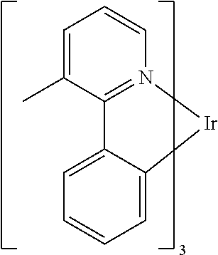 |
US20060240279 |
| Cross-linkable compounds |
 |
US20080220265 |
| Polythiophene based polymers and copolymers |
 |
WO2011075644 EP2350216 |
| Hole transporting materials |
| Triarylamines (e.g., TPD, α-NPD) |
 |
Appl. Phys. Lett. 51, 913 (1987) |
 |
U.S. Pat. No. 5,061,569 | |
 |
EP650955 | |
 |
J. Mater. Chem. 3, 319 (1993) | |
 |
Appl. Phys. Lett. 90, 183503 (2007) | |
 |
Appl. Phys. Lett. 90, 183503 (2007) | |
| Triarylamine on spirofluorene core |
 |
Synth. Met. 91, 209 (1997) |
| Arylamine carbazole compounds |
 |
Adv. Mater. 6, 677 (1994), US20080124572 |
| Triarylamine with (di)benzothio- phene/(di)benzofuran |
 |
US20070278938, US20080106190 US20110163302 |
| Indolocarbazoles |
 |
Synth. Met. 111, 421 (2000) |
| Isoindole compounds |
 |
Chem. Mater. 15, 3148 (2003) |
| Metal carbene complexes |
 |
US20080018221 |
| Phosphorescent OLED host materials |
| Red hosts |
| Arylcarbazoles |
 |
Appl. Phys. Lett. 78, 1622 (2001) |
| Metal 8-hydroxyquinolates (e.g., Alq3, BAlq) |
 |
Nature 395, 151 (1998) |
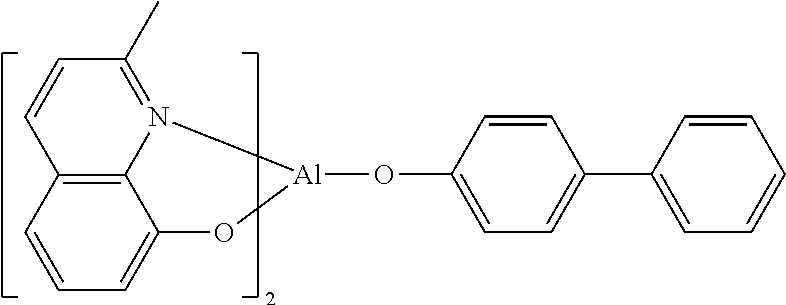 |
US20060202194 | |
 |
WO2005014551 | |
 |
WO2006072002 | |
| Metal phenoxybenzothiazole compounds |
 |
Appl. Phys. Lett. 90, 123509 (2007) |
| Conjugated oligomers and polymers (e.g., polyfluorene) |
 |
Org. Electron. 1, 15 (2000) |
| Aromatic fused rings |
 |
WO2009066779, WO2009066778, WO2009063833, US20090045731, US20090045730, WO2009008311, US20090008605, US20090009065 |
| Zinc complexes |
 |
WO2010056066 |
| Chrysene based compounds |
 |
WO2011086863 |
| Green hosts |
| Arylcarbazoles |
 |
Appl. Phys. Lett. 78, 1622 (2001) |
 |
US20030175553 | |
 |
WO2001039234 | |
| Aryltriphenylene compounds |
 |
US20060280965 |
 |
US20060280965 | |
 |
WO2009021126 | |
| Poly-fused heteroaryl compounds |
 |
US20090309488 US20090302743 US20100012931 |
| Donor acceptor type molecules |
 |
WO2008056746 |
 |
WO2010107244 | |
| Aza- carbazole/DBT/DBF |
 |
JP2008074939 |
 |
US20100187984 | |
| Polymers (e.g., PVK) |
 |
Appl. Phys. Lett. 77, 2280 (2000) |
| Spirofluorene compounds |
 |
WO2004093207 |
| Metal phenoxybenzooxazole compounds |
 |
WO2005089025 |
 |
WO2006132173 | |
 |
JP200511610 | |
| Spirofluorene-carbazole compounds |
 |
JP2007254297 |
 |
JP2007254297 | |
| Indolocarbazoles |
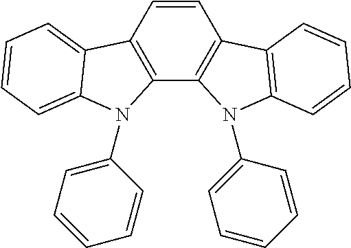 |
WO2007063796 |
 |
WO2007063754 | |
| 5-member ring electron deficient heterocycles (e.g., triazole, oxadiazole) |
 |
J. Appl. Phys. 90, 5048 (2001) |
 |
WO2004107822 | |
| Tetraphenylene complexes |
 |
US20050112407 |
| Metal phenoxypyridine compounds |
 |
WO2005030900 |
| Metal coordination complexes (e.g., Zn, Al with N{circumflex over ( )}N ligands) |
 |
US20040137268, US20040137267 |
| Blue hosts |
| Arylcarbazoles |
 |
Appl. Phys. Lett, 82, 2422 (2003) |
 |
US20070190359 | |
| Dibenzothio- phene/Dihenzofuran- carbazole compounds |
 |
WO2006114966, US20090167162 |
 |
US20090167162 | |
 |
WO2009086028 | |
 |
US20090030202, US20090017330 | |
 |
US20100084966 | |
| Silicon aryl compounds |
 |
US20050238919 |
 |
WO2009003898 | |
| Silicon/Germanium aryl compounds |
 |
EP2034538A |
| Aryl benzoyl ester |
 |
WO2006100298 |
| Carbazole linked by non- conjugated groups |
 |
US20040115476 |
| Aza-carbazoles |
 |
US20060121308 |
| High triplet metal organometallic complex |
 |
U.S. Pat. No. 7,154,114 |
| Phosphorescent dopants |
| Red dopants |
| Heavy metal porphyrins (e.g., PtOEP) |
 |
Nature 395, 151 (1998) |
| Iridium(III) organometallic complexes |
 |
Appl. Phys. Lett. 78, 1622 (2001) |
 |
US20030072964 | |
 |
US20030072964 | |
 |
US20060202194 | |
 |
US20060202194 | |
 |
US20070087321 | |
 |
US20080261076 US20100090591 | |
 |
US20070087321 | |
 |
Adv. Mater. 19, 739 (2007) | |
 |
WO2009100991 | |
 |
WO2008101842 | |
 |
U.S. Pat. No. 7,232,618 | |
| Platinum(II) organometallic complexes |
 |
WO2003040257 |
 |
US20070103060 | |
| Osmium(III) complexes |
 |
Chem. Mater. 17, 3532 (2005) |
| Ruthenium(II) complexes |
 |
Adv. Mater. 17, 1059 (2005) |
| Rhenium (I), (II), and (III) complexes |
 |
US20050244673 |
| Green dopants |
| Iridium(III) organometallic complexes |
 |
Inorg. Chem. 40, 1704 (2001) |
 |
US20020034656 | |
 |
U.S. Pat. No. 7,332,232 | |
 |
US20090108737 | |
 |
WO2010028151 | |
 |
EP1841834B | |
 |
US20060127696 | |
 |
US20090039776 | |
 |
U.S. Pat. No. 6,921,915 | |
 |
US20100244004 | |
 |
U.S. Pat. No. 6,687,266 | |
 |
Chem. Mater. 16, 2480 (2004) | |
 |
US20070190359 | |
 |
US20060008670 JP2007123392 | |
 |
WO2010086089, WO2011044988 | |
 |
Adv. Mater. 16, 2003 (2004) | |
 |
Angew. Chem. Int. Ed. 2006, 45, 7800 | |
 |
WO2009050290 | |
 |
US20090165846 | |
 |
US20080015355 | |
 |
US20010015432 | |
 |
US20100295032 | |
| Monomer for polymeric metal organometallic compounds |
 |
U.S. Pat. No. 7,250,226, U.S. Pat. No. 7,396,598 |
| Pt(II) organometallic complexes, including polydentate ligands |
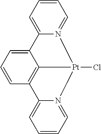 |
Appl. Phys. Lett. 86, 153505 (2005) |
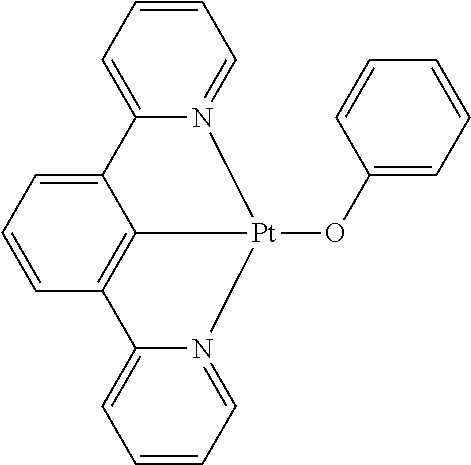 |
Appl. Phys. Lett. 86, 153505 (2005) | |
 |
Chem. Lett. 34, 592 (2005) | |
 |
WO2002015645 | |
 |
US20060263635 | |
 |
US20060182992 US20070103060 | |
| Cu complexes |
 |
WO2009000673 |
 |
US20070111026 | |
| Gold complexes |
 |
Chem. Commun. 2906 (2005) |
| Rhenium(III) complexes |
 |
Inorg. Chem. 42, 1248 (2003) |
| Osmium(II) complexes |
 |
U.S. Pat. No. 7,279,704 |
| Deuterated organometallic complexes |
 |
US20030138657 |
| Organometallic complexes with two or more metal centers |
 |
US20030152802 |
 |
U.S. Pat. No. 7,090,928 | |
| Blue dopants |
| Iridium(III) organometallic complexes |
 |
WO2002002714 |
 |
WO2006009024 | |
 |
US20060251923 US20110057559 US20110204333 | |
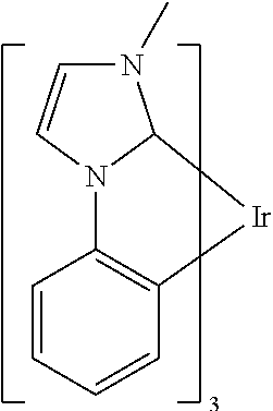 |
U.S. Pat. No. 7,393,599, WO2006056418, US20050260441, WO2005019373 | |
 |
U.S. Pat. No. 7,534,505 | |
 |
WO2011051404 | |
 |
U.S. Pat. No. 7,445,855 | |
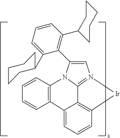 |
US20070190359, US20080297033 US20100148663 | |
 |
U.S. Pat. No. 7,338,722 | |
 |
US20020134984 | |
 |
Angew. Chem. Int. Ed. 47, 4542 (2008) | |
 |
Chem. Mater. 18, 5119 (2006) | |
 |
Inorg. Chem. 46, 4308 (2007) | |
 |
WO2005123873 | |
 |
WO2005123873 | |
 |
WO2007004380 | |
 |
WO2006082742 | |
| Osmium(II) complexes |
 |
U.S. Pat. No. 7,279,704 |
 |
Organometallics 23, 3745 (2004) | |
| Gold complexes |
|
Appl. Phys. Lett. 74, 1361 (1999) |
| Platinum(II) complexes |
 |
WO2006098120, WO2006103874 |
| Pt tetradentate complexes with at least one metal- carbene bond |
 |
U.S. Pat. No. 7,655,323 |
| Exciton/hole blocking layer materials |
| Bathocuprine compounds (e.g., BCP, BPhen) |
 |
Appl. Phys. Lett. 75, 4 (1999) |
 |
Appl. Phys. Lett. 79, 449 (2001) | |
| Metal 8-hydroxyquinolates (e.g., BAlq) |
 |
Appl. Phys. Lett. 81, 162 (2002) |
| 5-member ring electron deficient heterocycles such as triazole, oxadiazole, imidazole, benzoimidazole |
 |
Appl. Phys. Lett. 81, 162 (2002) |
| Triphenylene compounds |
 |
US20050025993 |
| Fluorinated aromatic compounds |
 |
Appl. Phys. Lett. 79, 156 (2001) |
| Phenothiazine- S-oxide |
 |
WO2008132085 |
| Silylated five-membered nitrogen, oxygen, sulfur or phosphorus dibenzoheterocycles |
 |
WO2010079051 |
| Aza-carbazoles |
 |
US20060121308 |
| Electron transporting materials |
| Anthracene- benzoimidazole compounds |
 |
WO2003060956 |
 |
US20090179554 | |
| Aza triphenylene derivatives |
 |
US20090115316 |
| Anthracene- benzothiazole compounds |
 |
Appl. Phys. Lett. 89, 063504 (2006) |
| Metal 8-hydroxyquinolates (e.g., Alq3, Zrq4) |
 |
Appl. Phys. Lett. 51, 913 (1987) U.S. Pat. No. 7,230,107 |
| Metal hydroxy- benoquinolates |
 |
Chem. Lett. 5, 905 (1993) |
| Bathocuprine compounds such as BCP, BPhen, etc |
 |
Appl. Phys. Lett. 91, 263503 (2007) |
 |
Appl. Phys. Lett. 79, 449 (2001) | |
| 5-member ring electron deficient heterocycles (e.g., triazole, oxadiazole, imidazole, benzoimidazole) |
 |
Appl. Phys. Lett. 74, 865 (1999) |
 |
Appl. Phys. Lett. 55, 1489 (1989) | |
 |
Jpn. J. Apply. Phys. 32, L917 (1993) | |
| Silole compounds |
 |
Org. Electron. 4, 113 (2003) |
| Arylborane compounds |
 |
J. Am. Chem. Soc. 120, 9714 (1998) |
| Fluorinated aromatic compounds |
 |
J. Am. Chem. Soc. 122, 1832 (2000) |
| Fullerene (e.g., C60) |
 |
US20090101870 |
| Triazine complexes |
 |
US20040036077 |
| Zn (N{circumflex over ( )}N) complexes |
 |
U.S. Pat. No. 6,528,187 |

Tetraphenylene (10.6 g, 35.0 mmol) synthesized according to Liebigs Ann. Chem. 704, 91-108 (1967), bis(pinacolato)diboron (8.8 g, 35.0 mmol), 4,4′-di-tert-butyl-2,2′-dipyridyl (1.9 g, 7.0 mmol), (1,5-cyclooctadiene)(methoxy)iridium(I) dimer (2.3 g, 3.5 mmol) and anhydrous cyclohexane (250 mL) were mixed at room temperature. The reaction mixture was bubbled with nitrogen for 15 min. The resultant mixture was refluxed for 14 hours. The solvent was removed in vacuo. The residue was purified by flash column chromatography using 25%-40% of DCM in hexane (with 0.5% triethylamine). The solid obtained was then mixed with 100 mL of MeCN and sonicated for 5 min at room temperature. The solid was filtered and dried under vacuum at 60° C. to afford 4,4,5,5-tetramethyl-2-(tetraphenylen-2-yl)-1,3,2-dioxaborolane (3.2 g,) as a white solid.
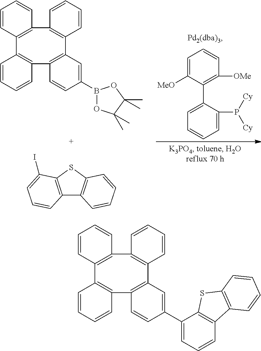
4,4,5,5-Tetramethyl-2-(tetraphenylen-2-yl)-1,3,2-dioxaborolane (1.9 g, 4.5 mmol), 4-iododibenzo[b,d]thiophene (2.0 g, 6.8 mmol), K3PO4 (1.9 g, 9.0 mmol) 2-dicyclohexylphosphino-2′,6′-dimethoxybiphenyl (0.7 g, 1.8 mmol), toluene (40 mL) and water (4 mL) were mixed at room temperature. The reaction mixture was bubbled with nitrogen for 30 min. Pd2(dba)3 (0.4 g, 0.45 mmol) was added. The mixture was bubbled with nitrogen for 15 min. The resultant mixture was refluxed for 70 hours. The reaction mixture was extracted by 3 L of 50% DCM/hexane. The extract was filtered through a silica pad and MgSO4. The solvent was removed in vacuo. The residue was purified by flash column chromatography using 10% then 15% of DCM in hexane. This product was mixed with 50 mL of heptane and bubbled with N2 for 15 min. The resultant mixture was refluxed for 1 hour. The solid was filtered and dried under vacuum at 60° C. to afford the desired product (1.6 g) as a white solid.

4,4,5,5-Tetramethyl-2-(tetraphenylen-2-yl)-1,3,2-dioxaborolane (2.8 g, 6.5 mmol), dioxane (150 mL), MeOH (50 mL) and CuBr2 solution (9.1 g, 39 mmol in 150 mL of H2O) were mixed at room temperature. The reaction mixture was bubbled with nitrogen for 15 min. The resultant mixture was refluxed for 140 hours. The reaction mixture was extracted by 50% of DCM in hexane. The extract was filtered through a silica pad and MgSO4. The solvent was removed in vacuo. The residue was purified by flash column chromatography using 15% of DCM in hexane to afford 2-bromotetraphenylene (2.2 g) as a white solid.

2-Bromotetraphenylene (3.1 g, 8.0 mmol), carbazole (8.0 g, 48.0 mmol), 2-dicyclohexylphosphino-2′,6′-dimethoxybiphenyl (3.3 g, 8.0 mmol), sodium tert-butoxide (3.8 g, 40.0 mmol) and toluene (100 mL) were mixed at room temperature. The reaction mixture was bubbled with nitrogen for 15 min. Pd2(dba)3 (1.8 g, 2.0 mmol) was added. The mixture was bubbled with nitrogen for 15 min. The resultant mixture was refluxed for 17 hours. The reaction mixture was filtered through a silica pad and MgSO4 and eluted by 50% of DCM in hexane. The solvent was removed in vacuo. This product was mixed with 600 mL of MeCN and bubbled with N2 for 30 min. The resultant mixture was refluxed for 1 hour and allowed to reach room temperature. The solid was filtered and dried under vacuum at 60° C. to afford the desired product (2.5 g) as a white solid. The triplet energy of Compounds 1 and 21, measured at 77 K in dilute THF solutions, are 410 nm and 456 nm, respectively.
In the OLED experiment, all device examples were fabricated by high vacuum (<10−7 Torr) thermal evaporation. The anode electrode is ˜800 Å of indium tin oxide (ITO). The cathode consisted of 10 Å of LiF followed by 1,000 Å of Al. All devices were encapsulated with a glass lid sealed with an epoxy resin in a nitrogen glove box (<1 ppm of H2O and O2) and a moisture getter was incorporated inside the package.
The organic stack of the Device Examples in Table 1 consists of sequentially, from the ITO surface, 100 Å of LG101 (purchased from LG Chem, Korea) as the hole injection layer (HIL), 250 Å of Compound A as the primary hole transport layer (HTL1), 300 Å of Compound 1 doped with 20% of the emitter Compound B as the emissive layer (EML), 50 Å of Compound C as ETL2 and 400 Å of Alq3 as ETL1.
Device Example 2 was fabricated in the same way except as Device Example 1 except that 300 Å instead of 400 Å of Alq3 as ETL1 was used.
Device Example 3 was fabricated in the same way as Device Example 1 except that 50 Å of Compound E as the secondary hole transport layer (HTL2) was inserted between the HTL1 and EML and 300 Å, instead of 400 Å, of Alq3 as ETL1 was used.
Device Comparative Example 1 and Device Comparative Example 2 were fabricated in the same way as Device Example 1 except Compound C and Compound D were used as the host compounds in Device Comparative Example 1 and Device Comparative Example 2, respectively.
The device data is summarized in Table 1 below:
| TABLE 1 | ||||
| 1931 CIE | At 1,000 cd/m2 | |||
| Device | Host | Alq3 | CIE | CIE | λ max | Voltage | LE | EQE | PE | |
| Example | HTL2 | 300 Å | Å | x | y | [nm] | [V] | [cd/A] | [%] | [lm/W] |
| Device | none | Cmpd 1 | 400 | 0.175 | 0.393 | 474 | 5.8 | 52.2 | 23.3 | 28.2 |
| Example 1 | ||||||||||
| Device | none | Cmpd 21 | 300 | 0.170 | 0.373 | 474 | 5.4 | 47.0 | 21.9 | 27.6 |
| Example 2 | ||||||||||
| Device | Cmpd E | Cmpd 21 | 300 | 0.170 | 0.381 | 474 | 5.4 | 54.7 | 25.1 | 31.8 |
| Example 3 | (50 Å) | |||||||||
| Device | none | Cmpd D | 400 | 0.179 | 0.408 | 474 | 5.8 | 46.5 | 20.3 | 25.2 |
| Comparative | ||||||||||
| Example 1 | ||||||||||
| Device | none | Cmpd C | 400 | 0.178 | 0.406 | 474 | 5.5 | 47.6 | 20.7 | 27.1 |
| Comparative | ||||||||||
| Example 2 | ||||||||||
Some of the compounds used in the devices are:

The organic stack of the Device Examples in Table 2 consists of sequentially, from the ITO surface, 100 Å of LG101 as the hole injection layer (HIL), 450 Å of Compound A as the hole transport layer (HTL1), 400 Å of Compound 21 doped with 10% of the emitter Compound F as the emissive layer (EML), 50 Å of Compound G as ETL2 and 350 Å of Alq3 as ETL1.
Device Comparative Example 3 was fabricated in the same way as Device Example 3 except CBP was used as the host.
The device data is summarized in Table 2.
| LT80 at | ||||||
| 1931 CIE | At 1,000 cd/m2 | 20 mA/cm2 | ||||
| Device | Host | CIE | CIE | λmax | Voltage | LE | EQE | PE | Lo | time |
| example | 300 Å | x | y | [nm] | [V] | [cd/A] | [%] | [Im/W] | [cd/m2] | [h] |
| Device | Cmpd 2 | 0.321 | 0.630 | 523 | 5.9 | 63.2 | 17.6 | 33.6 | 19909 | 178 |
| example 3 | ||||||||||
| Device | CBP | 0.319 | 0.630 | 522 | 5.1 | 63.6 | 17.7 | 39.5 | 19382 | 69 |
| comparative | ||||||||||
| example 3 | ||||||||||

The only difference between Device Example 1 and Device Comparative Examples 1 and 2 is the host. At 1000 cd/m2, Device Example 1 with Compound 1 as the host has an efficiency of 23.3% whereas Device Comparative Example 1 has an efficiency of 20.3% and Device Comparative Example 2 has an efficiency of 20.7%. Compound 1 as the host is shown to be superior to commonly used high performance hosts for blue phosphorescence OLED hosts such as Compound C and D. The increase in efficiency is presumably due to the increase of solid state triplet energy of the host in the EML because tetraphenylene acts as a sterically cumbersome block which reduces 7 stacking between host-host molecules and host-dopant molecules, particularly when the tetraphenylene compound has a low symmetry. The increase in efficiency can also be seen in Device Example 2 with Compound 21 as the host. Although the triplet energy of Compound 21 is not as high as the triplet energy of Compound 1, it is unexpectedly very suitable as a blue phosphorescence OLED host. The efficiency reaches 21.9%, higher than the efficiency of Device Comparative Examples 1 and 2. The efficiency can be further enhanced when a secondary hole transport layer (Compound E) is inserted between the HTL1 and EML as demonstrated in Device Example 3. A very high efficiency of 25.1% which is achieved.
Compound 21 was also tested as a host with a green phosphorescent emitter (Compound F). Device Example 3 with Compound 21 as the host has an efficiency of 17.6%. On the other hand, using a standard green phosphorescence OLED host CBP, Device Comparative Example 3 has an efficiency of 17.7%. Although the two device perform similarly, the lifetimes are very different. Device Example 3 with Compound 21 as the host shows a much superior lifetime. LT80 (the time to reach 80% of its initial luminance L0) at J=40 mA/cm2 is 178 hours compared to 69 hours of Device Comparative Example 3 with CBP as the host. The improvement is ˜200%.
The device data demonstrates that OLED with tetraphenylene compounds with low symmetry as hosts can achieve high efficiency and operation stability. In particular, due to the high triplet energy of the tetraphenylene, they are especially useful in blue and green phosphorescence OLEDs.
Claims (17)
1. A compound having a formula:

wherein R1-R16 are each independently selected from the group consisting of hydrogen, deuterium, halogen, alkyl, cycloalkyl, heteroalkyl, arylalkyl, alkoxy, aryloxy, amino, silyl, alkenyl, cycloalkenyl, heteroalkenyl, alkynyl, aryl, heteroaryl, acyl, carbonyl, carboxylic acid, ester, nitrile, isonitrile, sulfanyl, sulfinyl, sulfonyl, phosphino, and combinations thereof;
wherein at least one of R1-R16 comprises a chemical group selected from the group consisting of dibenzofuran, dibenzothiophene, dibenzoselenophene, triphenylene, fluorene, aza-carbazole, aza-dibenzofuran, aza-dibenzothiophene, aza-dibenzoselenophene, aza-triphenylene, and aza-fluorene; and
wherein the compound has the highest symmetry of C1.
2. The compound of claim 1 , wherein at least one of R1-R16 comprises a chemical group selected from the group consisting of dibenzofuran, dibenzothiophene, dibenzoselenophene, aza-dibenzofuran, aza-dibenzothiophene, and aza-dibenzoselenophene.
3. The compound of claim 1 , wherein at least one of R1-R16 comprises a chemical group selected from the group consisting of triphenylene, and aza-triphenylene.
4. The compound of claim 1 , wherein at least one of R1-R16 comprises a chemical group selected from the group consisting of dibenzofuran, dibenzothiophene, dibenzoselenophene, triphenylene, fluorene, aza-carbazole, aza-dibenzofuran, aza-dibenzothiophene, aza-dibenzoselenophene, aza-triphenylene, and aza-fluorene.
5. The compound of claim 1 , wherein at least one of R1-R16 comprises aza-carbazole.
6. The compound of claim 1 , wherein at least two of R1-R16 comprises a chemical group independently selected from the group consisting of dibenzofuran, dibenzothiophene, dibenzoselenophene, triphenylene, fluorene, aza-carbazole, aza-dibenzofuran, aza-dibenzothiophene, aza-dibenzoselenophene, aza-triphenylene, and aza-fluorene.
7. The compound of claim 1 , wherein at least two of R1-R16 comprises different chemical groups selected from the group consisting of dibenzofuran, dibenzothiophene, dibenzoselenphene, triphenylene, fluorene, aza-carbazole, aza-dibenzofuran, aza-dibenzothiophene, aza-dibenzoselenphene, aza-triphenylene, and aza-fluorene.
8. The compound of claim 1 , wherein the compound comprises at least two different chemical groups selected from the group consisting of dibenzofuran, dibenzothiophene, dibenzoselenophene, triphenylene, fluorene, aza-carbazole, aza-dibenzofuran, aza-dibenzothiophene, aza-dibenzoselenophene, aza-triphenylene, and aza-fluorene.
9. The compound of claim 1 , wherein at least one of R1-R16 is selected from the group consisting of dibenzofuran, dibenzothiophene, dibenzoselenophene, triphenylene, fluorene, aza-carbazole, aza-dibenzofuran, aza-dibenzothiophene, aza-dibenzoselenophene, aza-triphenylene, and aza-fluorene.
10. The compound of claim 1 , wherein the compound is selected from the group consisting of:


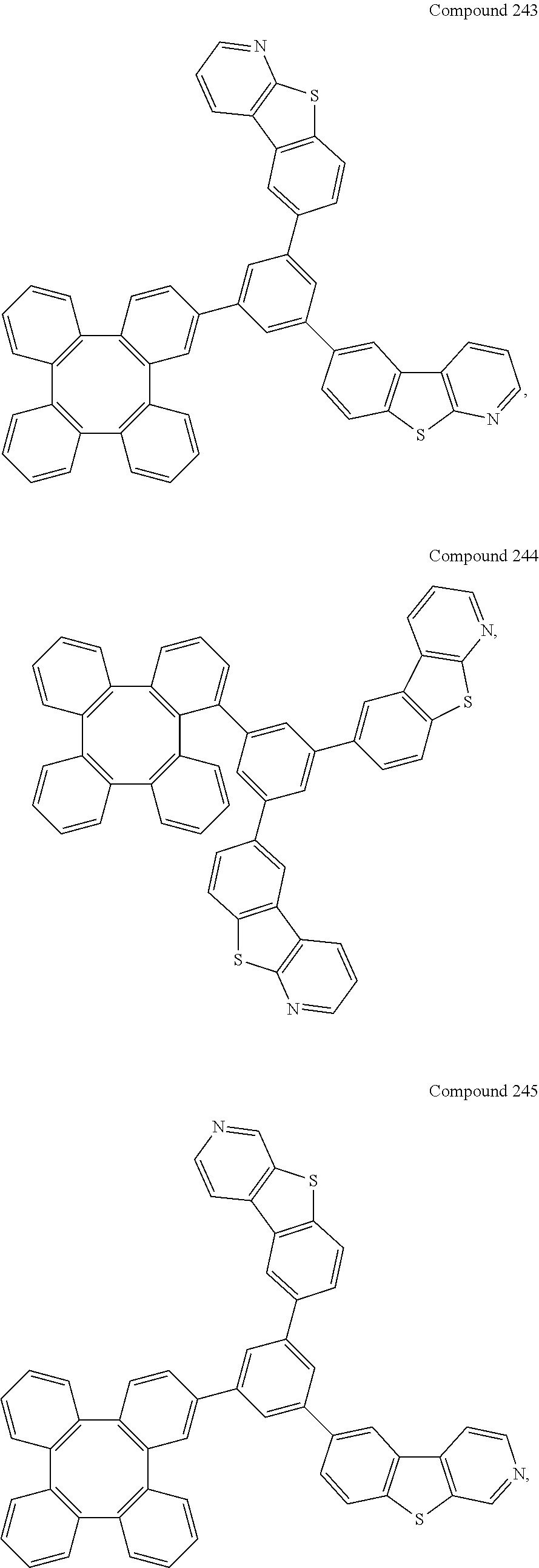


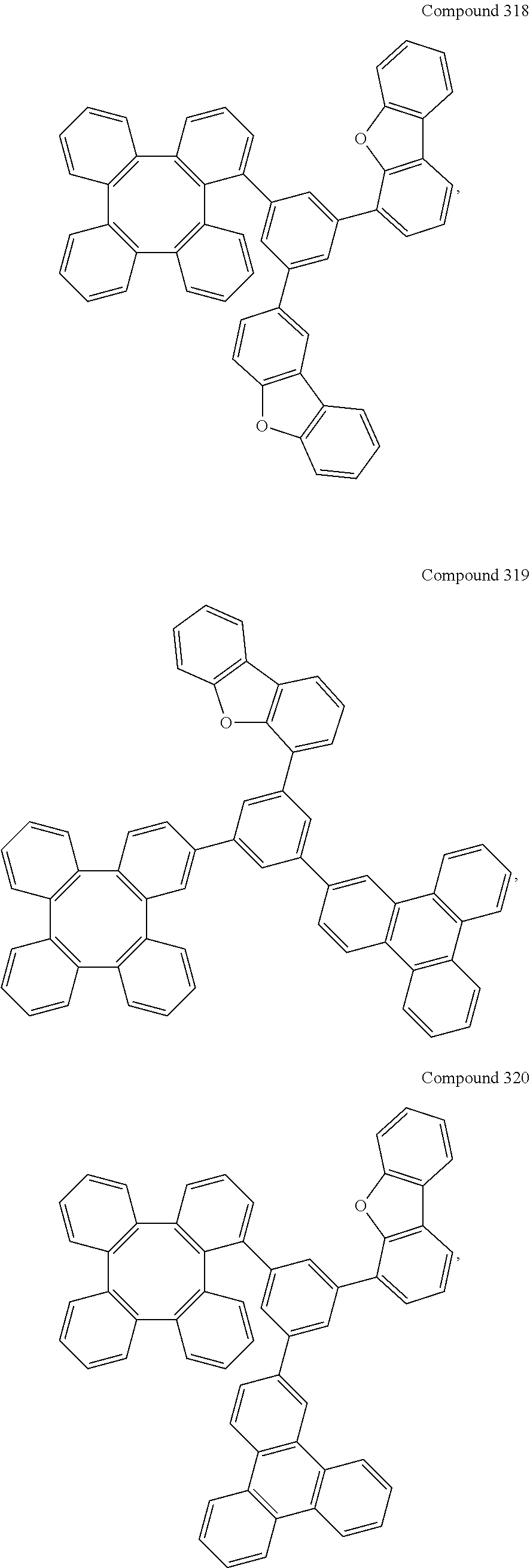


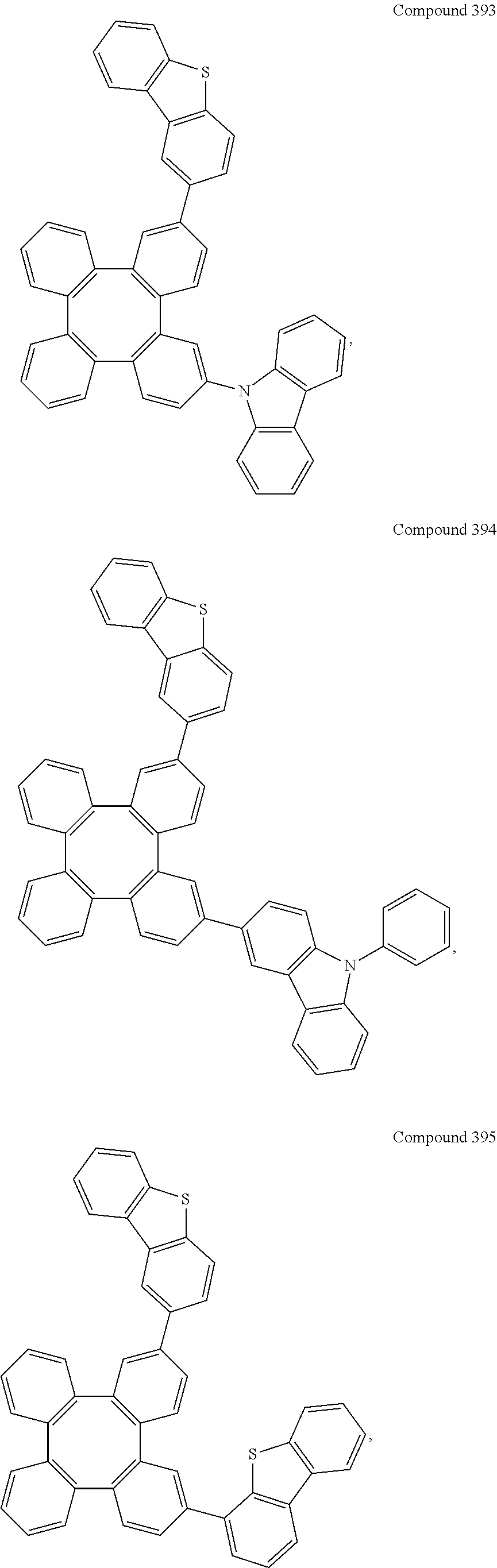


11. A device comprising one or more organic light emitting devices, at least one of the organic light emitting devices comprising:
an anode;
a cathode; and
an organic layer, disposed between the anode and the cathode, comprising a compound having the formula

wherein R1-R16 are each independently selected from the group consisting of hydrogen, deuterium, halogen, alkyl, cycloalkyl, heteroalkyl, arylalkyl, alkoxy, aryloxy, amino, silyl, alkenyl, cycloalkenyl, heteroalkenyl, alkynyl, aryl, heteroaryl, acyl, carbonyl, carboxylic acid, ester, nitrile, isonitrile, sulfanyl, sulfinyl, sulfonyl, phosphino, and combinations thereof;
wherein at least one of R1-R16 comprises a chemical group selected from the group consisting of dibenzofuran, dibenzothiophene, dibenzoselenphene, triphenylene, fluorene, aza-carbazole, aza-dibenzofuran, aza-dibenzothiophene, aza-dibenzoselenphene, aza-triphenylene, and aza-fluorene; and
wherein the compound has the highest symmetry of C1.
12. The device of claim 11 , wherein the organic layer is an emissive layer and the compound is a host.
13. The device of claim 11 , wherein the organic layer further comprises a phosphorescent emissive dopant, wherein the phosphorescent emissive dopant is a transition metal complex having at least one ligand or part of the ligand if the ligand is more than bidentate, selected from the group consisting of:


wherein each X1 to X13 are independently selected from the group consisting of carbon and nitrogen;
wherein X is selected from the group consisting of BR′, NR′, PR′, O, S, Se, C═O, S═O, SO2, CR′R″, SiR′R″, and GeR′R″;
wherein R′ and R″ are optionally fused or joined to form a ring;
wherein each Ra, Rb, Rc, and Rd may represent from mono substitution to the possible maximum number of substitution, or no substitution;
wherein R′, R″, Ra, Rb, Rc, and Rd are each independently selected from the group consisting of hydrogen, deuterium, halide, alkyl, cycloalkyl, heteroalkyl, arylalkyl, alkoxy, aryloxy, amino, silyl, alkenyl, cycloalkenyl, heteroalkenyl, alkynyl, aryl, heteroaryl, acyl, carbonyl, carboxylic acids, ester, nitrile, isonitrile, sulfanyl, sulfinyl, sulfonyl, phosphino, and combinations thereof; and
wherein any two adjacent substitutents of Ra, Rb, Rc, and Rd are optionally fused or joined to form a ring or form a multidentate ligand.
14. The device of claim 11 , wherein the organic layer is a charge carrier blocking layer and the compound having Formula I is a charge carrier blocking material in the organic layer.
15. The device of claim 11 , wherein the organic layer is a charge carrier transporting layer and the compound having Formula I is a charge carrier transporting material in the organic layer.
16. The device of claim 11 , wherein the device is selected from the group consisting of a consumer product, an electronic component module, an organic light-emitting device, and a lighting panel.
17. A formulation comprising the compound in claim 1 .
Priority Applications (2)
| Application Number | Priority Date | Filing Date | Title |
|---|---|---|---|
| US14/718,299 US10256411B2 (en) | 2015-05-21 | 2015-05-21 | Organic electroluminescent materials and devices |
| US15/359,597 US10109799B2 (en) | 2015-05-21 | 2016-11-22 | Organic electroluminescent materials and devices |
Applications Claiming Priority (1)
| Application Number | Priority Date | Filing Date | Title |
|---|---|---|---|
| US14/718,299 US10256411B2 (en) | 2015-05-21 | 2015-05-21 | Organic electroluminescent materials and devices |
Related Child Applications (1)
| Application Number | Title | Priority Date | Filing Date |
|---|---|---|---|
| US15/359,597 Continuation-In-Part US10109799B2 (en) | 2015-05-21 | 2016-11-22 | Organic electroluminescent materials and devices |
Publications (2)
| Publication Number | Publication Date |
|---|---|
| US20160343951A1 US20160343951A1 (en) | 2016-11-24 |
| US10256411B2 true US10256411B2 (en) | 2019-04-09 |
Family
ID=57324509
Family Applications (1)
| Application Number | Title | Priority Date | Filing Date |
|---|---|---|---|
| US14/718,299 Active 2036-06-22 US10256411B2 (en) | 2015-05-21 | 2015-05-21 | Organic electroluminescent materials and devices |
Country Status (1)
| Country | Link |
|---|---|
| US (1) | US10256411B2 (en) |
Cited By (1)
| Publication number | Priority date | Publication date | Assignee | Title |
|---|---|---|---|---|
| US20180287087A1 (en) * | 2017-03-28 | 2018-10-04 | Universal Display Corporation | Organic electroluminescent materials and devices |
Families Citing this family (9)
| Publication number | Priority date | Publication date | Assignee | Title |
|---|---|---|---|---|
| US10566547B2 (en) | 2016-07-11 | 2020-02-18 | Universal Display Corporation | Organic electroluminescent materials and devices |
| US11101434B2 (en) | 2017-04-21 | 2021-08-24 | Universal Display Corporation | Organic electroluminescent materials and devices |
| US11322691B2 (en) * | 2017-07-26 | 2022-05-03 | Universal Display Corporation | Organic electroluminescent materials and devices |
| US11917843B2 (en) * | 2017-07-26 | 2024-02-27 | Universal Display Corporation | Organic electroluminescent materials and devices |
| CN109651065B (en) * | 2017-10-12 | 2022-11-29 | 北京夏禾科技有限公司 | Tetraortho-phenylene anthracene compounds |
| US10978645B2 (en) | 2017-10-20 | 2021-04-13 | Beijing Summer Sprout Technology Co., Ltd. | Indolocarbazole tetraphenylene compounds |
| KR20230173735A (en) * | 2017-11-07 | 2023-12-27 | 미쯔비시 케미컬 주식회사 | Iridium complex compound, composition containing said compound and solvent, organic electroluminescent element containing said compound, display device, and illumination device |
| CN109928885B (en) | 2017-12-19 | 2022-11-29 | 北京夏禾科技有限公司 | tetra-o-phenylenetriarylamine compound |
| CN109659448B (en) * | 2017-12-27 | 2021-07-06 | 广州华睿光电材料有限公司 | Organic mixture, composition and organic electronic device |
Citations (123)
| Publication number | Priority date | Publication date | Assignee | Title |
|---|---|---|---|---|
| US4769292A (en) | 1987-03-02 | 1988-09-06 | Eastman Kodak Company | Electroluminescent device with modified thin film luminescent zone |
| US5061569A (en) | 1990-07-26 | 1991-10-29 | Eastman Kodak Company | Electroluminescent device with organic electroluminescent medium |
| US5247190A (en) | 1989-04-20 | 1993-09-21 | Cambridge Research And Innovation Limited | Electroluminescent devices |
| EP0650955A1 (en) | 1993-11-01 | 1995-05-03 | Hodogaya Chemical Co., Ltd. | Amine compound and electro-luminescence device comprising same |
| US5703436A (en) | 1994-12-13 | 1997-12-30 | The Trustees Of Princeton University | Transparent contacts for organic devices |
| US5707745A (en) | 1994-12-13 | 1998-01-13 | The Trustees Of Princeton University | Multicolor organic light emitting devices |
| US5834893A (en) | 1996-12-23 | 1998-11-10 | The Trustees Of Princeton University | High efficiency organic light emitting devices with light directing structures |
| US5844363A (en) | 1997-01-23 | 1998-12-01 | The Trustees Of Princeton Univ. | Vacuum deposited, non-polymeric flexible organic light emitting devices |
| US6013982A (en) | 1996-12-23 | 2000-01-11 | The Trustees Of Princeton University | Multicolor display devices |
| US6087196A (en) | 1998-01-30 | 2000-07-11 | The Trustees Of Princeton University | Fabrication of organic semiconductor devices using ink jet printing |
| US6091195A (en) | 1997-02-03 | 2000-07-18 | The Trustees Of Princeton University | Displays having mesa pixel configuration |
| US6097147A (en) | 1998-09-14 | 2000-08-01 | The Trustees Of Princeton University | Structure for high efficiency electroluminescent device |
| WO2001039234A2 (en) | 1999-11-24 | 2001-05-31 | The Trustees Of Princeton University | Organic light emitting diode having a blue phosphorescent molecule as an emitter |
| JP2001167884A (en) * | 1999-12-13 | 2001-06-22 | Nec Corp | Organic electroluminescent element |
| US6294398B1 (en) | 1999-11-23 | 2001-09-25 | The Trustees Of Princeton University | Method for patterning devices |
| US6303238B1 (en) | 1997-12-01 | 2001-10-16 | The Trustees Of Princeton University | OLEDs doped with phosphorescent compounds |
| US6337102B1 (en) | 1997-11-17 | 2002-01-08 | The Trustees Of Princeton University | Low pressure vapor phase deposition of organic thin films |
| WO2002002714A2 (en) | 2000-06-30 | 2002-01-10 | E.I. Du Pont De Nemours And Company | Electroluminescent iridium compounds with fluorinated phenylpyridines, phenylpyrimidines, and phenylquinolines and devices made with such compounds |
| WO2002015645A1 (en) | 2000-08-11 | 2002-02-21 | The Trustees Of Princeton University | Organometallic compounds and emission-shifting organic electrophosphorescence |
| US20020034656A1 (en) | 1998-09-14 | 2002-03-21 | Thompson Mark E. | Organometallic complexes as phosphorescent emitters in organic LEDs |
| US6416887B1 (en) * | 1998-11-11 | 2002-07-09 | Kabushiki Kaisha Toyota Chuo Kenkyusho | Organic electroluminescent element |
| US20020134984A1 (en) | 2001-02-01 | 2002-09-26 | Fuji Photo Film Co., Ltd. | Transition metal complex and light-emitting device |
| US20020158242A1 (en) | 1999-12-31 | 2002-10-31 | Se-Hwan Son | Electronic device comprising organic compound having p-type semiconducting characteristics |
| US6528187B1 (en) | 1998-09-08 | 2003-03-04 | Fuji Photo Film Co., Ltd. | Material for luminescence element and luminescence element using the same |
| WO2003040257A1 (en) | 2001-11-07 | 2003-05-15 | E. I. Du Pont De Nemours And Company | Electroluminescent platinum compounds and devices made with such compounds |
| US20030138657A1 (en) | 2000-12-07 | 2003-07-24 | Canon Kabushiki Kaisha | Deuterated semi-conducting organic compounds used for opto-electronic devices |
| WO2003060956A2 (en) | 2002-01-18 | 2003-07-24 | Lg Chem, Ltd. | New material for transporting electrons and organic electroluminescent display using the same |
| US20030152802A1 (en) | 2001-06-19 | 2003-08-14 | Akira Tsuboyama | Metal coordination compound and organic liminescence device |
| US20030151042A1 (en) | 2002-02-08 | 2003-08-14 | Hueschen Mark R. | Polarization field enhanced tunnel structures |
| US20030175553A1 (en) | 2001-12-28 | 2003-09-18 | Thompson Mark E. | White light emitting oleds from combined monomer and aggregate emission |
| US20030230980A1 (en) | 2002-06-18 | 2003-12-18 | Forrest Stephen R | Very low voltage, high efficiency phosphorescent oled in a p-i-n structure |
| US6687266B1 (en) | 2002-11-08 | 2004-02-03 | Universal Display Corporation | Organic light emitting materials and devices |
| US20040036077A1 (en) | 2002-08-22 | 2004-02-26 | Fuji Photo Film Co., Ltd. | Light emitting element |
| US20040137267A1 (en) | 2002-12-27 | 2004-07-15 | Fuji Photo Film Co., Ltd. | Organic electroluminescent device |
| US20040137268A1 (en) | 2002-12-27 | 2004-07-15 | Fuji Photo Film Co., Ltd. | Organic electroluminescent device |
| US20040174116A1 (en) | 2001-08-20 | 2004-09-09 | Lu Min-Hao Michael | Transparent electrodes |
| WO2004093207A2 (en) | 2003-04-15 | 2004-10-28 | Covion Organic Semiconductors Gmbh | Mixtures of matrix materials and organic semiconductors capable of emission, use of the same and electronic components containing said mixtures |
| WO2004107822A1 (en) | 2003-05-29 | 2004-12-09 | Nippon Steel Chemical Co., Ltd. | Organic electroluminescent element |
| US6835469B2 (en) | 2001-10-17 | 2004-12-28 | The University Of Southern California | Phosphorescent compounds and devices comprising the same |
| JP2005011610A (en) | 2003-06-18 | 2005-01-13 | Nippon Steel Chem Co Ltd | Organic electroluminescence device |
| US20050025993A1 (en) | 2003-07-25 | 2005-02-03 | Thompson Mark E. | Materials and structures for enhancing the performance of organic light emitting devices |
| WO2005014551A1 (en) | 2003-08-07 | 2005-02-17 | Nippon Steel Chemical Co., Ltd. | Aluminum chelate compelx for organic el material |
| WO2005019373A2 (en) | 2003-08-19 | 2005-03-03 | Basf Aktiengesellschaft | Transition metal complexes comprising carbene ligands serving as emitters for organic light-emitting diodes (oled's) |
| WO2005030900A1 (en) | 2003-09-25 | 2005-04-07 | Nippon Steel Chemical Co., Ltd. | Organic electroluminescent device |
| US20050112407A1 (en) | 2003-11-21 | 2005-05-26 | Fuji Photo Film Co., Ltd. | Organic electroluminescent device |
| US6921915B2 (en) | 2001-03-08 | 2005-07-26 | Canon Kabushiki Kaisha | Metal coordination compound, luminescence device and display apparatus |
| WO2005089025A1 (en) | 2004-03-15 | 2005-09-22 | Nippon Steel Chemical Co., Ltd. | Organic electroluminescent device |
| US20050238919A1 (en) | 2004-04-23 | 2005-10-27 | Fuji Photo Film Co., Ltd. | Organic electroluminescent device |
| US20050244673A1 (en) | 2002-08-27 | 2005-11-03 | Fujitsu Limited | Organometallic complex, organic EL element and organic EL display |
| US20050260441A1 (en) | 2004-05-18 | 2005-11-24 | Thompson Mark E | Luminescent compounds with carbene ligands |
| US20050260449A1 (en) | 2004-05-18 | 2005-11-24 | Robert Walters | Complexes with tridentate ligands |
| WO2005123873A1 (en) | 2004-06-17 | 2005-12-29 | Konica Minolta Holdings, Inc. | Organic electroluminescent device material, organic electroluminescent device, display and illuminating device |
| US20060008670A1 (en) | 2004-07-06 | 2006-01-12 | Chun Lin | Organic light emitting materials and devices |
| WO2006009024A1 (en) | 2004-07-23 | 2006-01-26 | Konica Minolta Holdings, Inc. | Organic electroluminescent device, display and illuminating device |
| WO2006056418A2 (en) | 2004-11-25 | 2006-06-01 | Basf Aktiengesellschaft | Use of transition metal carbene complexes in organic light-emitting diodes (oleds) |
| WO2006072002A2 (en) | 2004-12-30 | 2006-07-06 | E.I. Dupont De Nemours And Company | Organometallic complexes |
| US7087321B2 (en) | 2003-04-22 | 2006-08-08 | Universal Display Corporation | Organic light emitting devices having reduced pixel shrinkage |
| WO2006082742A1 (en) | 2005-02-04 | 2006-08-10 | Konica Minolta Holdings, Inc. | Organic electroluminescent device material, organic electroluminescent device, display and illuminating device |
| US7090928B2 (en) | 2003-04-01 | 2006-08-15 | The University Of Southern California | Binuclear compounds |
| US20060202194A1 (en) | 2005-03-08 | 2006-09-14 | Jeong Hyun C | Red phosphorescene compounds and organic electroluminescence device using the same |
| WO2006098120A1 (en) | 2005-03-16 | 2006-09-21 | Konica Minolta Holdings, Inc. | Organic electroluminescent device material and organic electroluminescent device |
| WO2006100298A1 (en) | 2005-03-24 | 2006-09-28 | Basf Aktiengesellschaft | Use of compounds containing aromatic or heteroaromatic rings linked via carbonyl group-containing groups, for use as matrix materials in organic light-emitting diodes |
| WO2006103874A1 (en) | 2005-03-29 | 2006-10-05 | Konica Minolta Holdings, Inc. | Organic electroluminescent device material, organic electroluminescent device, display and illuminating device |
| US20060240279A1 (en) | 2005-04-21 | 2006-10-26 | Vadim Adamovich | Non-blocked phosphorescent OLEDs |
| WO2006114966A1 (en) | 2005-04-18 | 2006-11-02 | Konica Minolta Holdings, Inc. | Organic electroluminescent device, display and illuminating device |
| US20060251923A1 (en) | 2005-05-06 | 2006-11-09 | Chun Lin | Stability OLED materials and devices |
| EP1725079A1 (en) | 2004-03-11 | 2006-11-22 | Mitsubishi Chemical Corporation | Composition for charge-transporting film and ion compound, charge-transporting film and organic electroluminescent device using same, and method for manufacturing organic electroluminescent device and method for producing charge-transporting film |
| US20060263635A1 (en) | 2005-05-06 | 2006-11-23 | Fuji Photo Film Co., Ltd. | Organic electroluminescent device |
| WO2006132173A1 (en) | 2005-06-07 | 2006-12-14 | Nippon Steel Chemical Co., Ltd. | Organic metal complex and organic electroluminescent device using same |
| US20060280965A1 (en) | 2005-05-31 | 2006-12-14 | Raymond Kwong | Triphenylene hosts in phosphorescent light emitting diodes |
| US7154114B2 (en) | 2004-05-18 | 2006-12-26 | Universal Display Corporation | Cyclometallated iridium carbene complexes for use as hosts |
| WO2007002683A2 (en) | 2005-06-27 | 2007-01-04 | E. I. Du Pont De Nemours And Company | Electrically conductive polymer compositions |
| WO2007004380A1 (en) | 2005-07-01 | 2007-01-11 | Konica Minolta Holdings, Inc. | Organic electroluminescent element material, organic electroluminescent element, display device, and lighting equipment |
| JP2007123392A (en) | 2005-10-26 | 2007-05-17 | Konica Minolta Holdings Inc | Organic electroluminescence element, display device and lighting device |
| WO2007063754A1 (en) | 2005-12-01 | 2007-06-07 | Nippon Steel Chemical Co., Ltd. | Compound for organic electroluminescent element and organic electroluminescent element |
| WO2007063796A1 (en) | 2005-12-01 | 2007-06-07 | Nippon Steel Chemical Co., Ltd. | Organic electroluminescent device |
| US7250226B2 (en) | 2001-08-31 | 2007-07-31 | Nippon Hoso Kyokai | Phosphorescent compound, a phosphorescent composition and an organic light-emitting device |
| US20070190359A1 (en) | 2006-02-10 | 2007-08-16 | Knowles David B | Metal complexes of cyclometallated imidazo[1,2-ƒ]phenanthridine and diimidazo[1,2-a:1',2'-c]quinazoline ligands and isoelectronic and benzannulated analogs thereof |
| JP2007254297A (en) | 2006-03-20 | 2007-10-04 | Nippon Steel Chem Co Ltd | Luminescent layer compound and organic electroluminescent device |
| US20070278938A1 (en) | 2006-04-26 | 2007-12-06 | Idemitsu Kosan Co., Ltd. | Aromatic amine derivative and electroluminescence device using the same |
| US20080015355A1 (en) | 2004-06-28 | 2008-01-17 | Thomas Schafer | Electroluminescent Metal Complexes With Triazoles And Benzotriazoles |
| US7332232B2 (en) | 2004-02-03 | 2008-02-19 | Universal Display Corporation | OLEDs utilizing multidentate ligand systems |
| US7338722B2 (en) | 2003-03-24 | 2008-03-04 | The University Of Southern California | Phenyl and fluorenyl substituted phenyl-pyrazole complexes of Ir |
| JP2008074939A (en) | 2006-09-21 | 2008-04-03 | Konica Minolta Holdings Inc | ORGANIC ELECTROLUMINESCENT ELEMENT MATERIAL, ORGANIC ELECTROLUMINESCENT ELEMENT, DISPLAY DEVICE AND LIGHTING DEVICE |
| US20080106190A1 (en) | 2006-08-23 | 2008-05-08 | Idemitsu Kosan Co., Ltd. | Aromatic amine derivatives and organic electroluminescent device using same |
| WO2008056746A1 (en) | 2006-11-09 | 2008-05-15 | Nippon Steel Chemical Co., Ltd. | Compound for organic electroluminescent device and organic electroluminescent device |
| US20080124572A1 (en) | 2006-11-24 | 2008-05-29 | Idemitsu Kosan Co., Ltd. | Aromatic amine derivative and organic electroluminescence device using the same |
| US7393599B2 (en) | 2004-05-18 | 2008-07-01 | The University Of Southern California | Luminescent compounds with carbene ligands |
| US7396598B2 (en) | 2001-06-20 | 2008-07-08 | Showa Denko K.K. | Light emitting material and organic light-emitting device |
| WO2008101842A1 (en) | 2007-02-23 | 2008-08-28 | Basf Se | Electroluminescent metal complexes with benzotriazoles |
| US20080220265A1 (en) | 2006-12-08 | 2008-09-11 | Universal Display Corporation | Cross-linkable Iridium Complexes and Organic Light-Emitting Devices Using the Same |
| US7431968B1 (en) | 2001-09-04 | 2008-10-07 | The Trustees Of Princeton University | Process and apparatus for organic vapor jet deposition |
| US7445855B2 (en) | 2004-05-18 | 2008-11-04 | The University Of Southern California | Cationic metal-carbene complexes |
| WO2008132085A1 (en) | 2007-04-26 | 2008-11-06 | Basf Se | Silanes containing phenothiazine-s-oxide or phenothiazine-s,s-dioxide groups and the use thereof in oleds |
| US20080297033A1 (en) | 2006-02-10 | 2008-12-04 | Knowles David B | Blue phosphorescent imidazophenanthridine materials |
| WO2009000673A2 (en) | 2007-06-22 | 2008-12-31 | Basf Se | Light emitting cu(i) complexes |
| US20090009065A1 (en) | 2007-07-07 | 2009-01-08 | Idemitsu Kosan Co., Ltd. | Organic electroluminescence device and material for organic electroluminescence device |
| WO2009003898A1 (en) | 2007-07-05 | 2009-01-08 | Basf Se | Organic light-emitting diodes containing carbene transition metal complex emitters and at least one compound selected from disilylcarbazoles, disilyldibenzofurans, disilyldibenzothiophenes, disilyldibenzophospholes, disilyldibenzothiophene s-oxides and disilyldibenzothiophene s,s-dioxides |
| US20090008605A1 (en) | 2007-07-07 | 2009-01-08 | Idemitsu Kosan Co., Ltd. | Naphthalene derivative, material for organic electroluminescence device, and organic electroluminescence device using the same |
| US20090017330A1 (en) | 2007-07-10 | 2009-01-15 | Idemitsu Kosan Co., Ltd. | Material for organic electroluminescence device and organic electroluminescence device utilizing the same |
| WO2009008311A1 (en) | 2007-07-07 | 2009-01-15 | Idemitsu Kosan Co., Ltd. | Chrysene derivative and organic electroluminescent device using the same |
| US20090030202A1 (en) | 2007-07-10 | 2009-01-29 | Idemitsu Kosan Co., Ltd. | Material for organic electroluminescent element and organic electroluminescent element employing the same |
| WO2009018009A1 (en) | 2007-07-27 | 2009-02-05 | E. I. Du Pont De Nemours And Company | Aqueous dispersions of electrically conducting polymers containing inorganic nanoparticles |
| US20090039776A1 (en) | 2007-08-09 | 2009-02-12 | Canon Kabushiki Kaisha | Organometallic complex and organic light-emitting element using same |
| WO2009021126A2 (en) | 2007-08-08 | 2009-02-12 | Universal Display Corporation | Benzo-fused thiophene or benzo-fused furan compounds comprising a triphenylene group |
| US20090045731A1 (en) | 2007-07-07 | 2009-02-19 | Idemitsu Kosan Co., Ltd. | Organic electroluminescence device and material for organic electroluminescence device |
| US20090045730A1 (en) | 2007-07-07 | 2009-02-19 | Idemitsu Kosan Co., Ltd. | Organic electroluminescence device and material for organic electroluminescence device |
| EP2034538A1 (en) | 2006-06-02 | 2009-03-11 | Idemitsu Kosan Co., Ltd. | Material for organic electroluminescence element, and organic electroluminescence element using the material |
| WO2009050290A1 (en) | 2007-10-17 | 2009-04-23 | Basf Se | Transition metal complexes having bridged carbene ligands and the use thereof in oleds |
| US20090101870A1 (en) | 2007-10-22 | 2009-04-23 | E. I. Du Pont De Nemours And Company | Electron transport bi-layers and devices made with such bi-layers |
| US20090108737A1 (en) | 2006-12-08 | 2009-04-30 | Raymond Kwong | Light-emitting organometallic complexes |
| US20090115316A1 (en) | 2007-11-02 | 2009-05-07 | Shiying Zheng | Organic electroluminescent device having an azatriphenylene derivative |
| US7534505B2 (en) | 2004-05-18 | 2009-05-19 | The University Of Southern California | Organometallic compounds for use in electroluminescent devices |
| WO2009063833A1 (en) | 2007-11-15 | 2009-05-22 | Idemitsu Kosan Co., Ltd. | Benzochrysene derivative and organic electroluminescent device using the same |
| WO2009062578A1 (en) | 2007-11-12 | 2009-05-22 | Merck Patent Gmbh | Organic electroluminescent devices comprising azomethine-metal complexes |
| WO2009066778A1 (en) | 2007-11-22 | 2009-05-28 | Idemitsu Kosan Co., Ltd. | Organic el element and solution containing organic el material |
| WO2009066779A1 (en) | 2007-11-22 | 2009-05-28 | Idemitsu Kosan Co., Ltd. | Organic el element |
| US20090165846A1 (en) | 2005-09-07 | 2009-07-02 | Universitaet Braunschweig | Triplet emitter having condensed five-membered rings |
| US20090167162A1 (en) | 2007-12-28 | 2009-07-02 | Universal Display Corporation | Dibenzothiophene-containing materials in phosphorescent light emitting diodes |
| WO2009086028A2 (en) | 2007-12-28 | 2009-07-09 | Universal Display Corporation | Carbazole-containing materials in phosphorescent light emitting diodes |
| US20090179554A1 (en) | 2006-05-11 | 2009-07-16 | Hitoshi Kuma | Organic electroluminescent device |
| WO2009100991A1 (en) | 2008-02-12 | 2009-08-20 | Basf Se | Electroluminescent metal complexes with dibenzo[f,h]quinoxalines |
| US7740956B2 (en) * | 2002-12-27 | 2010-06-22 | Fujifilm Corporation | Organic electroluminescent device |
-
2015
- 2015-05-21 US US14/718,299 patent/US10256411B2/en active Active
Patent Citations (129)
| Publication number | Priority date | Publication date | Assignee | Title |
|---|---|---|---|---|
| US4769292A (en) | 1987-03-02 | 1988-09-06 | Eastman Kodak Company | Electroluminescent device with modified thin film luminescent zone |
| US5247190A (en) | 1989-04-20 | 1993-09-21 | Cambridge Research And Innovation Limited | Electroluminescent devices |
| US5061569A (en) | 1990-07-26 | 1991-10-29 | Eastman Kodak Company | Electroluminescent device with organic electroluminescent medium |
| EP0650955A1 (en) | 1993-11-01 | 1995-05-03 | Hodogaya Chemical Co., Ltd. | Amine compound and electro-luminescence device comprising same |
| US5703436A (en) | 1994-12-13 | 1997-12-30 | The Trustees Of Princeton University | Transparent contacts for organic devices |
| US5707745A (en) | 1994-12-13 | 1998-01-13 | The Trustees Of Princeton University | Multicolor organic light emitting devices |
| US5834893A (en) | 1996-12-23 | 1998-11-10 | The Trustees Of Princeton University | High efficiency organic light emitting devices with light directing structures |
| US6013982A (en) | 1996-12-23 | 2000-01-11 | The Trustees Of Princeton University | Multicolor display devices |
| US5844363A (en) | 1997-01-23 | 1998-12-01 | The Trustees Of Princeton Univ. | Vacuum deposited, non-polymeric flexible organic light emitting devices |
| US6091195A (en) | 1997-02-03 | 2000-07-18 | The Trustees Of Princeton University | Displays having mesa pixel configuration |
| US6337102B1 (en) | 1997-11-17 | 2002-01-08 | The Trustees Of Princeton University | Low pressure vapor phase deposition of organic thin films |
| US6303238B1 (en) | 1997-12-01 | 2001-10-16 | The Trustees Of Princeton University | OLEDs doped with phosphorescent compounds |
| US6087196A (en) | 1998-01-30 | 2000-07-11 | The Trustees Of Princeton University | Fabrication of organic semiconductor devices using ink jet printing |
| US6528187B1 (en) | 1998-09-08 | 2003-03-04 | Fuji Photo Film Co., Ltd. | Material for luminescence element and luminescence element using the same |
| US6097147A (en) | 1998-09-14 | 2000-08-01 | The Trustees Of Princeton University | Structure for high efficiency electroluminescent device |
| US20020034656A1 (en) | 1998-09-14 | 2002-03-21 | Thompson Mark E. | Organometallic complexes as phosphorescent emitters in organic LEDs |
| US6416887B1 (en) * | 1998-11-11 | 2002-07-09 | Kabushiki Kaisha Toyota Chuo Kenkyusho | Organic electroluminescent element |
| US6294398B1 (en) | 1999-11-23 | 2001-09-25 | The Trustees Of Princeton University | Method for patterning devices |
| US6468819B1 (en) | 1999-11-23 | 2002-10-22 | The Trustees Of Princeton University | Method for patterning organic thin film devices using a die |
| WO2001039234A2 (en) | 1999-11-24 | 2001-05-31 | The Trustees Of Princeton University | Organic light emitting diode having a blue phosphorescent molecule as an emitter |
| US20010006741A1 (en) * | 1999-12-13 | 2001-07-05 | Nec Corporation | Organic electroluminescent device |
| JP2001167884A (en) * | 1999-12-13 | 2001-06-22 | Nec Corp | Organic electroluminescent element |
| US20020158242A1 (en) | 1999-12-31 | 2002-10-31 | Se-Hwan Son | Electronic device comprising organic compound having p-type semiconducting characteristics |
| WO2002002714A2 (en) | 2000-06-30 | 2002-01-10 | E.I. Du Pont De Nemours And Company | Electroluminescent iridium compounds with fluorinated phenylpyridines, phenylpyrimidines, and phenylquinolines and devices made with such compounds |
| WO2002015645A1 (en) | 2000-08-11 | 2002-02-21 | The Trustees Of Princeton University | Organometallic compounds and emission-shifting organic electrophosphorescence |
| US20030138657A1 (en) | 2000-12-07 | 2003-07-24 | Canon Kabushiki Kaisha | Deuterated semi-conducting organic compounds used for opto-electronic devices |
| US20020134984A1 (en) | 2001-02-01 | 2002-09-26 | Fuji Photo Film Co., Ltd. | Transition metal complex and light-emitting device |
| US6921915B2 (en) | 2001-03-08 | 2005-07-26 | Canon Kabushiki Kaisha | Metal coordination compound, luminescence device and display apparatus |
| US20030152802A1 (en) | 2001-06-19 | 2003-08-14 | Akira Tsuboyama | Metal coordination compound and organic liminescence device |
| US7396598B2 (en) | 2001-06-20 | 2008-07-08 | Showa Denko K.K. | Light emitting material and organic light-emitting device |
| US20040174116A1 (en) | 2001-08-20 | 2004-09-09 | Lu Min-Hao Michael | Transparent electrodes |
| US7250226B2 (en) | 2001-08-31 | 2007-07-31 | Nippon Hoso Kyokai | Phosphorescent compound, a phosphorescent composition and an organic light-emitting device |
| US7431968B1 (en) | 2001-09-04 | 2008-10-07 | The Trustees Of Princeton University | Process and apparatus for organic vapor jet deposition |
| US6835469B2 (en) | 2001-10-17 | 2004-12-28 | The University Of Southern California | Phosphorescent compounds and devices comprising the same |
| WO2003040257A1 (en) | 2001-11-07 | 2003-05-15 | E. I. Du Pont De Nemours And Company | Electroluminescent platinum compounds and devices made with such compounds |
| US20030175553A1 (en) | 2001-12-28 | 2003-09-18 | Thompson Mark E. | White light emitting oleds from combined monomer and aggregate emission |
| WO2003060956A2 (en) | 2002-01-18 | 2003-07-24 | Lg Chem, Ltd. | New material for transporting electrons and organic electroluminescent display using the same |
| US20030151042A1 (en) | 2002-02-08 | 2003-08-14 | Hueschen Mark R. | Polarization field enhanced tunnel structures |
| US20030230980A1 (en) | 2002-06-18 | 2003-12-18 | Forrest Stephen R | Very low voltage, high efficiency phosphorescent oled in a p-i-n structure |
| US20040036077A1 (en) | 2002-08-22 | 2004-02-26 | Fuji Photo Film Co., Ltd. | Light emitting element |
| US20050244673A1 (en) | 2002-08-27 | 2005-11-03 | Fujitsu Limited | Organometallic complex, organic EL element and organic EL display |
| US6687266B1 (en) | 2002-11-08 | 2004-02-03 | Universal Display Corporation | Organic light emitting materials and devices |
| US20040137267A1 (en) | 2002-12-27 | 2004-07-15 | Fuji Photo Film Co., Ltd. | Organic electroluminescent device |
| US20040137268A1 (en) | 2002-12-27 | 2004-07-15 | Fuji Photo Film Co., Ltd. | Organic electroluminescent device |
| US7740956B2 (en) * | 2002-12-27 | 2010-06-22 | Fujifilm Corporation | Organic electroluminescent device |
| US7338722B2 (en) | 2003-03-24 | 2008-03-04 | The University Of Southern California | Phenyl and fluorenyl substituted phenyl-pyrazole complexes of Ir |
| US7090928B2 (en) | 2003-04-01 | 2006-08-15 | The University Of Southern California | Binuclear compounds |
| WO2004093207A2 (en) | 2003-04-15 | 2004-10-28 | Covion Organic Semiconductors Gmbh | Mixtures of matrix materials and organic semiconductors capable of emission, use of the same and electronic components containing said mixtures |
| US7087321B2 (en) | 2003-04-22 | 2006-08-08 | Universal Display Corporation | Organic light emitting devices having reduced pixel shrinkage |
| WO2004107822A1 (en) | 2003-05-29 | 2004-12-09 | Nippon Steel Chemical Co., Ltd. | Organic electroluminescent element |
| JP2005011610A (en) | 2003-06-18 | 2005-01-13 | Nippon Steel Chem Co Ltd | Organic electroluminescence device |
| US20050025993A1 (en) | 2003-07-25 | 2005-02-03 | Thompson Mark E. | Materials and structures for enhancing the performance of organic light emitting devices |
| WO2005014551A1 (en) | 2003-08-07 | 2005-02-17 | Nippon Steel Chemical Co., Ltd. | Aluminum chelate compelx for organic el material |
| WO2005019373A2 (en) | 2003-08-19 | 2005-03-03 | Basf Aktiengesellschaft | Transition metal complexes comprising carbene ligands serving as emitters for organic light-emitting diodes (oled's) |
| WO2005030900A1 (en) | 2003-09-25 | 2005-04-07 | Nippon Steel Chemical Co., Ltd. | Organic electroluminescent device |
| US7858211B2 (en) | 2003-11-21 | 2010-12-28 | Fujifilm Corporation | Organic electroluminescent device |
| US7468212B2 (en) * | 2003-11-21 | 2008-12-23 | Fujifilm Corporation | Organic electroluminescent device |
| US20050112407A1 (en) | 2003-11-21 | 2005-05-26 | Fuji Photo Film Co., Ltd. | Organic electroluminescent device |
| US7332232B2 (en) | 2004-02-03 | 2008-02-19 | Universal Display Corporation | OLEDs utilizing multidentate ligand systems |
| EP1725079A1 (en) | 2004-03-11 | 2006-11-22 | Mitsubishi Chemical Corporation | Composition for charge-transporting film and ion compound, charge-transporting film and organic electroluminescent device using same, and method for manufacturing organic electroluminescent device and method for producing charge-transporting film |
| WO2005089025A1 (en) | 2004-03-15 | 2005-09-22 | Nippon Steel Chemical Co., Ltd. | Organic electroluminescent device |
| US20050238919A1 (en) | 2004-04-23 | 2005-10-27 | Fuji Photo Film Co., Ltd. | Organic electroluminescent device |
| US7445855B2 (en) | 2004-05-18 | 2008-11-04 | The University Of Southern California | Cationic metal-carbene complexes |
| US7154114B2 (en) | 2004-05-18 | 2006-12-26 | Universal Display Corporation | Cyclometallated iridium carbene complexes for use as hosts |
| US7393599B2 (en) | 2004-05-18 | 2008-07-01 | The University Of Southern California | Luminescent compounds with carbene ligands |
| US7534505B2 (en) | 2004-05-18 | 2009-05-19 | The University Of Southern California | Organometallic compounds for use in electroluminescent devices |
| US20050260441A1 (en) | 2004-05-18 | 2005-11-24 | Thompson Mark E | Luminescent compounds with carbene ligands |
| US20050260449A1 (en) | 2004-05-18 | 2005-11-24 | Robert Walters | Complexes with tridentate ligands |
| US7279704B2 (en) | 2004-05-18 | 2007-10-09 | The University Of Southern California | Complexes with tridentate ligands |
| WO2005123873A1 (en) | 2004-06-17 | 2005-12-29 | Konica Minolta Holdings, Inc. | Organic electroluminescent device material, organic electroluminescent device, display and illuminating device |
| US20080015355A1 (en) | 2004-06-28 | 2008-01-17 | Thomas Schafer | Electroluminescent Metal Complexes With Triazoles And Benzotriazoles |
| US20060008670A1 (en) | 2004-07-06 | 2006-01-12 | Chun Lin | Organic light emitting materials and devices |
| WO2006009024A1 (en) | 2004-07-23 | 2006-01-26 | Konica Minolta Holdings, Inc. | Organic electroluminescent device, display and illuminating device |
| US20080018221A1 (en) | 2004-11-25 | 2008-01-24 | Basf Aktiengesellschaft | Use Of Transition Metal Carbene Complexes In Organic Light-Emitting Diodes (Oleds) |
| WO2006056418A2 (en) | 2004-11-25 | 2006-06-01 | Basf Aktiengesellschaft | Use of transition metal carbene complexes in organic light-emitting diodes (oleds) |
| WO2006072002A2 (en) | 2004-12-30 | 2006-07-06 | E.I. Dupont De Nemours And Company | Organometallic complexes |
| WO2006082742A1 (en) | 2005-02-04 | 2006-08-10 | Konica Minolta Holdings, Inc. | Organic electroluminescent device material, organic electroluminescent device, display and illuminating device |
| US20060202194A1 (en) | 2005-03-08 | 2006-09-14 | Jeong Hyun C | Red phosphorescene compounds and organic electroluminescence device using the same |
| WO2006098120A1 (en) | 2005-03-16 | 2006-09-21 | Konica Minolta Holdings, Inc. | Organic electroluminescent device material and organic electroluminescent device |
| WO2006100298A1 (en) | 2005-03-24 | 2006-09-28 | Basf Aktiengesellschaft | Use of compounds containing aromatic or heteroaromatic rings linked via carbonyl group-containing groups, for use as matrix materials in organic light-emitting diodes |
| WO2006103874A1 (en) | 2005-03-29 | 2006-10-05 | Konica Minolta Holdings, Inc. | Organic electroluminescent device material, organic electroluminescent device, display and illuminating device |
| WO2006114966A1 (en) | 2005-04-18 | 2006-11-02 | Konica Minolta Holdings, Inc. | Organic electroluminescent device, display and illuminating device |
| US20060240279A1 (en) | 2005-04-21 | 2006-10-26 | Vadim Adamovich | Non-blocked phosphorescent OLEDs |
| US20060263635A1 (en) | 2005-05-06 | 2006-11-23 | Fuji Photo Film Co., Ltd. | Organic electroluminescent device |
| US20060251923A1 (en) | 2005-05-06 | 2006-11-09 | Chun Lin | Stability OLED materials and devices |
| US20060280965A1 (en) | 2005-05-31 | 2006-12-14 | Raymond Kwong | Triphenylene hosts in phosphorescent light emitting diodes |
| WO2006132173A1 (en) | 2005-06-07 | 2006-12-14 | Nippon Steel Chemical Co., Ltd. | Organic metal complex and organic electroluminescent device using same |
| WO2007002683A2 (en) | 2005-06-27 | 2007-01-04 | E. I. Du Pont De Nemours And Company | Electrically conductive polymer compositions |
| WO2007004380A1 (en) | 2005-07-01 | 2007-01-11 | Konica Minolta Holdings, Inc. | Organic electroluminescent element material, organic electroluminescent element, display device, and lighting equipment |
| US20090165846A1 (en) | 2005-09-07 | 2009-07-02 | Universitaet Braunschweig | Triplet emitter having condensed five-membered rings |
| JP2007123392A (en) | 2005-10-26 | 2007-05-17 | Konica Minolta Holdings Inc | Organic electroluminescence element, display device and lighting device |
| WO2007063796A1 (en) | 2005-12-01 | 2007-06-07 | Nippon Steel Chemical Co., Ltd. | Organic electroluminescent device |
| WO2007063754A1 (en) | 2005-12-01 | 2007-06-07 | Nippon Steel Chemical Co., Ltd. | Compound for organic electroluminescent element and organic electroluminescent element |
| US20070190359A1 (en) | 2006-02-10 | 2007-08-16 | Knowles David B | Metal complexes of cyclometallated imidazo[1,2-ƒ]phenanthridine and diimidazo[1,2-a:1',2'-c]quinazoline ligands and isoelectronic and benzannulated analogs thereof |
| US20080297033A1 (en) | 2006-02-10 | 2008-12-04 | Knowles David B | Blue phosphorescent imidazophenanthridine materials |
| JP2007254297A (en) | 2006-03-20 | 2007-10-04 | Nippon Steel Chem Co Ltd | Luminescent layer compound and organic electroluminescent device |
| US20070278938A1 (en) | 2006-04-26 | 2007-12-06 | Idemitsu Kosan Co., Ltd. | Aromatic amine derivative and electroluminescence device using the same |
| US20090179554A1 (en) | 2006-05-11 | 2009-07-16 | Hitoshi Kuma | Organic electroluminescent device |
| EP2034538A1 (en) | 2006-06-02 | 2009-03-11 | Idemitsu Kosan Co., Ltd. | Material for organic electroluminescence element, and organic electroluminescence element using the material |
| US20080106190A1 (en) | 2006-08-23 | 2008-05-08 | Idemitsu Kosan Co., Ltd. | Aromatic amine derivatives and organic electroluminescent device using same |
| JP2008074939A (en) | 2006-09-21 | 2008-04-03 | Konica Minolta Holdings Inc | ORGANIC ELECTROLUMINESCENT ELEMENT MATERIAL, ORGANIC ELECTROLUMINESCENT ELEMENT, DISPLAY DEVICE AND LIGHTING DEVICE |
| WO2008056746A1 (en) | 2006-11-09 | 2008-05-15 | Nippon Steel Chemical Co., Ltd. | Compound for organic electroluminescent device and organic electroluminescent device |
| US20080124572A1 (en) | 2006-11-24 | 2008-05-29 | Idemitsu Kosan Co., Ltd. | Aromatic amine derivative and organic electroluminescence device using the same |
| US20080220265A1 (en) | 2006-12-08 | 2008-09-11 | Universal Display Corporation | Cross-linkable Iridium Complexes and Organic Light-Emitting Devices Using the Same |
| US20090108737A1 (en) | 2006-12-08 | 2009-04-30 | Raymond Kwong | Light-emitting organometallic complexes |
| WO2008101842A1 (en) | 2007-02-23 | 2008-08-28 | Basf Se | Electroluminescent metal complexes with benzotriazoles |
| WO2008132085A1 (en) | 2007-04-26 | 2008-11-06 | Basf Se | Silanes containing phenothiazine-s-oxide or phenothiazine-s,s-dioxide groups and the use thereof in oleds |
| WO2009000673A2 (en) | 2007-06-22 | 2008-12-31 | Basf Se | Light emitting cu(i) complexes |
| WO2009003898A1 (en) | 2007-07-05 | 2009-01-08 | Basf Se | Organic light-emitting diodes containing carbene transition metal complex emitters and at least one compound selected from disilylcarbazoles, disilyldibenzofurans, disilyldibenzothiophenes, disilyldibenzophospholes, disilyldibenzothiophene s-oxides and disilyldibenzothiophene s,s-dioxides |
| US20090045731A1 (en) | 2007-07-07 | 2009-02-19 | Idemitsu Kosan Co., Ltd. | Organic electroluminescence device and material for organic electroluminescence device |
| WO2009008311A1 (en) | 2007-07-07 | 2009-01-15 | Idemitsu Kosan Co., Ltd. | Chrysene derivative and organic electroluminescent device using the same |
| US20090045730A1 (en) | 2007-07-07 | 2009-02-19 | Idemitsu Kosan Co., Ltd. | Organic electroluminescence device and material for organic electroluminescence device |
| US20090009065A1 (en) | 2007-07-07 | 2009-01-08 | Idemitsu Kosan Co., Ltd. | Organic electroluminescence device and material for organic electroluminescence device |
| US20090008605A1 (en) | 2007-07-07 | 2009-01-08 | Idemitsu Kosan Co., Ltd. | Naphthalene derivative, material for organic electroluminescence device, and organic electroluminescence device using the same |
| US20090030202A1 (en) | 2007-07-10 | 2009-01-29 | Idemitsu Kosan Co., Ltd. | Material for organic electroluminescent element and organic electroluminescent element employing the same |
| US20090017330A1 (en) | 2007-07-10 | 2009-01-15 | Idemitsu Kosan Co., Ltd. | Material for organic electroluminescence device and organic electroluminescence device utilizing the same |
| WO2009018009A1 (en) | 2007-07-27 | 2009-02-05 | E. I. Du Pont De Nemours And Company | Aqueous dispersions of electrically conducting polymers containing inorganic nanoparticles |
| WO2009021126A2 (en) | 2007-08-08 | 2009-02-12 | Universal Display Corporation | Benzo-fused thiophene or benzo-fused furan compounds comprising a triphenylene group |
| US20090039776A1 (en) | 2007-08-09 | 2009-02-12 | Canon Kabushiki Kaisha | Organometallic complex and organic light-emitting element using same |
| WO2009050290A1 (en) | 2007-10-17 | 2009-04-23 | Basf Se | Transition metal complexes having bridged carbene ligands and the use thereof in oleds |
| US20090101870A1 (en) | 2007-10-22 | 2009-04-23 | E. I. Du Pont De Nemours And Company | Electron transport bi-layers and devices made with such bi-layers |
| US20090115316A1 (en) | 2007-11-02 | 2009-05-07 | Shiying Zheng | Organic electroluminescent device having an azatriphenylene derivative |
| WO2009062578A1 (en) | 2007-11-12 | 2009-05-22 | Merck Patent Gmbh | Organic electroluminescent devices comprising azomethine-metal complexes |
| WO2009063833A1 (en) | 2007-11-15 | 2009-05-22 | Idemitsu Kosan Co., Ltd. | Benzochrysene derivative and organic electroluminescent device using the same |
| WO2009066779A1 (en) | 2007-11-22 | 2009-05-28 | Idemitsu Kosan Co., Ltd. | Organic el element |
| WO2009066778A1 (en) | 2007-11-22 | 2009-05-28 | Idemitsu Kosan Co., Ltd. | Organic el element and solution containing organic el material |
| US20090167162A1 (en) | 2007-12-28 | 2009-07-02 | Universal Display Corporation | Dibenzothiophene-containing materials in phosphorescent light emitting diodes |
| WO2009086028A2 (en) | 2007-12-28 | 2009-07-09 | Universal Display Corporation | Carbazole-containing materials in phosphorescent light emitting diodes |
| WO2009100991A1 (en) | 2008-02-12 | 2009-08-20 | Basf Se | Electroluminescent metal complexes with dibenzo[f,h]quinoxalines |
Non-Patent Citations (46)
Cited By (2)
| Publication number | Priority date | Publication date | Assignee | Title |
|---|---|---|---|---|
| US20180287087A1 (en) * | 2017-03-28 | 2018-10-04 | Universal Display Corporation | Organic electroluminescent materials and devices |
| US10910577B2 (en) * | 2017-03-28 | 2021-02-02 | Universal Display Corporation | Organic electroluminescent materials and devices |
Also Published As
| Publication number | Publication date |
|---|---|
| US20160343951A1 (en) | 2016-11-24 |
Similar Documents
| Publication | Publication Date | Title |
|---|---|---|
| US11944000B2 (en) | Organic electroluminescent materials and devices | |
| US12201012B2 (en) | Organic electroluminescent materials and devices | |
| US12274165B2 (en) | Organic electroluminescent materials and devices | |
| US9755159B2 (en) | Organic materials for OLEDs | |
| US10461260B2 (en) | Organic electroluminescent materials and devices | |
| US9647218B2 (en) | Organic electroluminescent materials and devices | |
| US10177316B2 (en) | Organic electroluminescent materials and devices | |
| US10256411B2 (en) | Organic electroluminescent materials and devices | |
| US9419225B2 (en) | Organic electroluminescent materials and devices | |
| US10109799B2 (en) | Organic electroluminescent materials and devices | |
| US10566546B2 (en) | Organic electroluminescent materials and devices | |
| US10038151B2 (en) | Organic electroluminescent materials and devices | |
| US9647217B2 (en) | Organic electroluminescent materials and devices | |
| US10707423B2 (en) | Organic electroluminescent materials and devices | |
| US10208026B2 (en) | Organic electroluminescent materials and devices | |
| US9312499B1 (en) | Organic electroluminescent materials and devices | |
| US9711730B2 (en) | Organic electroluminescent materials and devices | |
| US9780316B2 (en) | Organic electroluminescent materials and devices | |
| US9386657B2 (en) | Organic Electroluminescent materials and devices | |
| US9478758B1 (en) | Organic electroluminescent materials and devices | |
| US9871212B2 (en) | Organic electroluminescent materials and devices | |
| US9761814B2 (en) | Organic light-emitting materials and devices | |
| US9741941B2 (en) | Organic electroluminescent materials and devices | |
| US20250183166A1 (en) | Organic Electroluminescent Materials and Devices |
Legal Events
| Date | Code | Title | Description |
|---|---|---|---|
| AS | Assignment |
Owner name: UNIVERSAL DISPLAY CORPORATION, NEW JERSEY Free format text: ASSIGNMENT OF ASSIGNORS INTEREST;ASSIGNORS:KWONG, RAYMOND;LAM, SZE KUI;REEL/FRAME:035688/0660 Effective date: 20150521 |
|
| STCF | Information on status: patent grant |
Free format text: PATENTED CASE |
|
| MAFP | Maintenance fee payment |
Free format text: PAYMENT OF MAINTENANCE FEE, 4TH YEAR, LARGE ENTITY (ORIGINAL EVENT CODE: M1551); ENTITY STATUS OF PATENT OWNER: LARGE ENTITY Year of fee payment: 4 |