US10247892B2 - Optical transceiver module having a partitioned housing - Google Patents
Optical transceiver module having a partitioned housing Download PDFInfo
- Publication number
- US10247892B2 US10247892B2 US15/242,017 US201615242017A US10247892B2 US 10247892 B2 US10247892 B2 US 10247892B2 US 201615242017 A US201615242017 A US 201615242017A US 10247892 B2 US10247892 B2 US 10247892B2
- Authority
- US
- United States
- Prior art keywords
- housing
- housing portion
- arrangement
- optical transceiver
- tosa
- Prior art date
- Legal status (The legal status is an assumption and is not a legal conclusion. Google has not performed a legal analysis and makes no representation as to the accuracy of the status listed.)
- Active
Links
Images


Classifications
-
- G—PHYSICS
- G02—OPTICS
- G02B—OPTICAL ELEMENTS, SYSTEMS OR APPARATUS
- G02B6/00—Light guides; Structural details of arrangements comprising light guides and other optical elements, e.g. couplings
- G02B6/24—Coupling light guides
- G02B6/42—Coupling light guides with opto-electronic elements
- G02B6/4201—Packages, e.g. shape, construction, internal or external details
- G02B6/4256—Details of housings
-
- G—PHYSICS
- G02—OPTICS
- G02B—OPTICAL ELEMENTS, SYSTEMS OR APPARATUS
- G02B6/00—Light guides; Structural details of arrangements comprising light guides and other optical elements, e.g. couplings
- G02B6/24—Coupling light guides
- G02B6/42—Coupling light guides with opto-electronic elements
- G02B6/4201—Packages, e.g. shape, construction, internal or external details
- G02B6/4246—Bidirectionally operating package structures
-
- G—PHYSICS
- G02—OPTICS
- G02B—OPTICAL ELEMENTS, SYSTEMS OR APPARATUS
- G02B6/00—Light guides; Structural details of arrangements comprising light guides and other optical elements, e.g. couplings
- G02B6/24—Coupling light guides
- G02B6/42—Coupling light guides with opto-electronic elements
- G02B6/4201—Packages, e.g. shape, construction, internal or external details
- G02B6/4256—Details of housings
- G02B6/426—Details of housings mounting, engaging or coupling of the package to a board, a frame or a panel
- G02B6/4261—Packages with mounting structures to be pluggable or detachable, e.g. having latches or rails
-
- G—PHYSICS
- G02—OPTICS
- G02B—OPTICAL ELEMENTS, SYSTEMS OR APPARATUS
- G02B6/00—Light guides; Structural details of arrangements comprising light guides and other optical elements, e.g. couplings
- G02B6/24—Coupling light guides
- G02B6/42—Coupling light guides with opto-electronic elements
- G02B6/4201—Packages, e.g. shape, construction, internal or external details
- G02B6/4274—Electrical aspects
- G02B6/4277—Protection against electromagnetic interference [EMI], e.g. shielding means
-
- G—PHYSICS
- G02—OPTICS
- G02B—OPTICAL ELEMENTS, SYSTEMS OR APPARATUS
- G02B6/00—Light guides; Structural details of arrangements comprising light guides and other optical elements, e.g. couplings
- G02B6/24—Coupling light guides
- G02B6/42—Coupling light guides with opto-electronic elements
- G02B6/4201—Packages, e.g. shape, construction, internal or external details
- G02B6/4274—Electrical aspects
- G02B6/428—Electrical aspects containing printed circuit boards [PCB]
- G02B6/4281—Electrical aspects containing printed circuit boards [PCB] the printed circuit boards being flexible
-
- G—PHYSICS
- G02—OPTICS
- G02B—OPTICAL ELEMENTS, SYSTEMS OR APPARATUS
- G02B6/00—Light guides; Structural details of arrangements comprising light guides and other optical elements, e.g. couplings
- G02B6/24—Coupling light guides
- G02B6/42—Coupling light guides with opto-electronic elements
- G02B6/4292—Coupling light guides with opto-electronic elements the light guide being disconnectable from the opto-electronic element, e.g. mutually self aligning arrangements
Definitions
- the present disclosure is related to optical transceivers modules and more particularly to an optical transceiver module that includes a partitioned housing that is small-form factor (SFF) compatible and provides separate portions for mounting and alignment of respective optical subassemblies to decrease manufacturing complexity, manufacturing time per unit, and increase overall yield.
- SFF small-form factor
- Optical transceivers are used to transmit and receive optical signals for various applications including, without limitation, internet data centers, cable TV broadband, and fiber to the home (FTTH) applications.
- Optical transceivers provide higher speeds and bandwidth over longer distances, for example, as compared to transmission over copper cables.
- the desire to provide higher speeds in smaller optical transceiver modules for a lower cost has presented challenges, for example, with respect to maintaining optical efficiency (power), thermal management, and manufacturing yield.
- Optical transceivers can include one or more transmitter optical subassemblies (TOSAs) and receiver optical subassemblies (ROSAs) for the purpose of transmitting and receiving optical signals.
- TOSAs transmitter optical subassemblies
- ROSAs receiver optical subassemblies
- FIG. 1 schematically illustrates an embodiment of an optical transceiver including a multi-channel transmitter optical subassembly (TOSA) and multi-channel receiver optical subassembly (ROSA).
- TOSA multi-channel transmitter optical subassembly
- ROSA multi-channel receiver optical subassembly
- FIG. 2A is a top plan view of a first portion of an optical transceiver module housing configured to couple to a transmitter optical subassembly (TOSA) arrangement, in accordance with an embodiment of the present disclosure.
- TOSA transmitter optical subassembly
- FIG. 2B is a top plan view of a second portion of an optical transceiver module housing configured to couple to a receiver optical subassembly (ROSA) arrangement, in accordance with an embodiment of the present disclosure.
- ROSA receiver optical subassembly
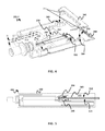
- FIG. 3A shows a perspective view of the first and second portions of the optical transceiver module housing of FIGS. 2A and 2B , respectively, prior to coupling of the same to form an assembled optical transceiver module, in accordance with an embodiment of the present disclosure.
- FIG. 3B shows a perspective view of an assembled optical transceiver module, in accordance with an embodiment of the present disclosure.
- FIG. 4 shows a perspective view of a second portion of the optical transceiver module housing of FIG. 2B , in accordance with an embodiment of the present disclosure.
- FIG. 5 is a side plan view of the assembled optical transceiver module of FIG. 3B having a printed circuit board (PCB) assembly coupled thereto, in accordance with an embodiment of the present disclosure.
- PCB printed circuit board
- Optical transceiver modules often include transmitter optical subassemblies (TOSAs) and receiver optical subassemblies (ROSAs) within a housing or body.
- An optical transceiver module may operate as a stand-alone optical transceiver, or may be integrated into a secondary housing that comports with, for instance, a small form-factor (SFF) housing standard such as the one outlined within the “QSFP+28 Gb/s 4 ⁇ Pluggable Transceiver Solution (QSFP28)” specification published on Jun. 29, 2015 by the SFF Committee.
- SFF small form-factor
- Such small form-factor housings introduce significant dimensional constraints that reduce the overall workspace within a transceiver housing which increases manufacturing complexity, error rates, and overall time to produce each optical transceiver module.
- a transceiver module having a partitioned housing e.g., a bifurcated or multi-segment housing
- a partitioned housing e.g., a bifurcated or multi-segment housing
- Technicians may thus perform at least partial assembly and testing of each optical subassembly arrangement in parallel and in relative isolation without necessarily interrupting and/or waiting on completion of the other.
- each separate portion of the partitioned housing provides a dedicated workspace for coupling associated subassembly components.
- Each separate portion may lie flat on a tabletop, for instance, which may further simplify manufacturing processes and provide a wide-range of acceptance angles for performing soldering, insertion and coupling of components, visual inspection, fiber routing, and so on.
- a technician may simply “flip” one portion of the partitioned housing over onto the other to couple the portions together and to collectively form an assembled optical transceiver module.
- the ROSA housing portion of the partitioned housing may be “flipped” onto the TOSA housing portion, with the TOSA housing portion forming the base (or bottom) of the assembled optical transceiver module.
- the ROSA housing portion may be accurately referred to as having a “flip over” configuration, whereby the ROSA arrangement faces the TOSA arrangement in a upside down manner when their respective housing portions are coupled together.
- Each of the TOSA and ROSA housing portions of the housing may include corresponding mateable features designed to interlock/mate with each other to form essentially a monolithic or integral optical transceiver module housing.
- the assembled optical transceiver module may then include a single compartment formed by the respective housing portions or may include a plurality of partitions defined by, for instance, a shield or other internal structure that separates ROSA and TOSA housing portions for purposes of electrical isolation, thermal conductivity, and RF shielding, for example.
- the assembled optical transceiver module may then be inserted into a QSFP+ or other SFF secondary housing, for instance, depending on a desired configuration.
- an optical transceiver module consistent with an embodiment of the present disclosure is defined by housing separable into at least two portions, namely at least a first portion having a TOSA arrangement (which may be referred to as a TOSA housing portion) and a second portion having a ROSA arrangement (which may be referred to as a ROSA housing portion).
- Each of the first and second portions include a base that provides one or more substantially planar mounting surfaces for coupling to associated ROSA/TOSA arrangements and associated circuitry.
- a plurality of sidewalls may extend substantially vertically from each base and provide a compartment/cavity there between to receive associated ROSA/TOSA components.
- At least one sidewall of each base may include an LC port receptacle designed to couple to a respective LC connector and receive the other's LC connector such that when the TOSA and ROSA housing portions are coupled together each LC connector extends in parallel from the same end of the assembled optical transceiver module. Once coupled, the assembled optical transceiver module may fully enclose the TOSA and ROSA arrangement and prevent the ingress of dust and other contaminants.
- channel wavelengths refer to the wavelengths associated with optical channels and may include a specified wavelength band around a center wavelength.
- the channel wavelengths may be defined by an International Telecommunication (ITU) standard such as the ITU-T dense wavelength division multiplexing (DWDM) grid.
- ITU International Telecommunication
- DWDM dense wavelength division multiplexing
- the optical transceiver 100 transmits and receives four (4) channels using four different channel wavelengths ( ⁇ 1 , ⁇ 2 , ⁇ 3 , ⁇ 4 ) and may be capable of transmission rates of at least about 25 gigabits (Gbs) per channel or more.
- the channel wavelengths ⁇ 1 , ⁇ 2 , ⁇ 3 , ⁇ 4 may be 1270 nm, 1290 nm, 1310 nm, and 1330 nm, respectively.
- the optical transceiver 100 may also be capable of both short transmission distances of tens of meters, for example, to distances of 2 kilometers or more.
- the optical transceiver 100 may be used, for example, in internet data center applications or fiber to the home (FTTH) applications.
- the optical transceiver 100 implements a Quad Small Form-Factor Pluggable (QSFP) transceiver.
- QSFP Quad Small Form-Factor Pluggable
- the optical transceiver 100 may be implemented within a QSFP transceiver that comports with the QSFP28 specification as discussed above.
- the aspects and embodiments disclosed herein may be used within other transceiver types and is not necessarily limited to QSFP or QFSP+ transceivers.
- the optical transceiver 100 may be configured for dense wavelength division multiplexing (DWDM) or course wavelength division multiplexing (CWDM), depending on a desired configuration.
- DWDM dense wavelength division multiplexing
- CWDM course wavelength division multiplexing
- the optical transceiver 100 includes a transceiver housing 102 that may include a multi-channel TOSA arrangement 110 for transmitting optical signals on different channel wavelengths, and a multi-channel ROSA 112 for receiving optical signals on different channel wavelengths within a single transceiver housing, as will be discussed further herein.
- a transmit connecting circuit 104 and a receive connecting circuit 108 provide electrical connections to the multi-channel TOSA arrangement 110 and the multi-channel ROSA arrangement 112 , respectively, within the transceiver housing 102 .
- the transmit connecting circuit 104 and the receive connecting circuit 108 may communicate with external systems via data bus 103 .
- data bus 103 is a 38-pin connector that comports with physical connector QSFP standards and data communication protocols.
- the transmit connecting circuit 104 electrically couples to the electronic components in the multi-channel TOSA arrangement 110 , e.g., laser assemblies, and the receive connecting circuit 108 electrically couples to the electronic components in the multi-channel ROSA 112 , e.g., an arrayed waveguide grating (AWG), detectors, amplification circuitry and so on.
- the transmit connecting circuit 104 and the receive connecting circuit 108 include at least conductive paths to provide electrical connections, and may also include additional circuitry.
- the multi-channel TOSA arrangement 110 transmits and multiplexes multiple different channel wavelengths, and is coupled to an optical interface port 114 .
- the optical interface port 114 may include an LC connector port, although other connector types are also within the scope of this disclosure.
- the LC connector receptacle provides optical connections to the multi-channel TOSA arrangement 110 , and provides optical connections to the multi-channel ROSA 112 .
- the LC connector receptacle may be configured to receive and be coupled to a mating LC connector 116 such that transmit optical fiber 122 of the external fibers 124 optically couples to the multi-channel arrangement TOSA 110 , and the receive optical fiber 117 of the external fibers 124 optically couples to the multi-channel ROSA 112 .
- the multi-channel TOSA arrangement 110 can include multiple laser packages and optics for producing associated channel wavelengths, and can couple the same into the transmit optical fiber 122 .
- the lasers in the multi-channel TOSA arrangement 110 can convert electrical data signals (TX_D 1 to TX_D 4 ) received via the transmit connecting circuit 104 into modulated optical signals transmitted over transmit optical fiber 122 .
- the lasers may include, for example, distributed feedback (DFB) lasers with diffraction gratings. In other cases, the lasers may comprise electro-absorption modulated laser (EML) laser diode packages.
- the multi-channel TOSA arrangement 110 may also include monitor photodiodes for monitoring the light emitted by the lasers.
- the multi-channel TOSA arrangement 110 may further include one or more temperature control devices, such as a resistive heater and/or a thermoelectric cooler (TEC), for controlling a temperature of the lasers, for example, to control or stabilize the laser wavelengths.
- TEC thermoelectric cooler
- the multi-channel ROSA 112 can include demultiplexing optics such as an AWG device and a plurality of detectors such as photodiode packages configured to receive de-multiplexed channel wavelengths.
- the ROSA 112 can use the detectors and associated circuitry (e.g., a TIA) to detect, amplify, and convert de-multiplexed channel wavelengths and can provide the same as electrical data signals, e.g., RX_D 1 to RX_D 4 .
- first and second portions 205 - 1 and 205 - 2 of an optical transceiver module housing 205 are shown in accordance with an embodiment of the present disclosure.
- An example assembled optical transceiver module 400 having both the first and second portions 205 - 1 and 205 - 2 coupled together is shown and described in greater detail below with reference to FIG. 3B .
- Each of the first and second portions 205 - 1 and 205 - 2 will now be discussed in turn.
- FIG. 2A shows a top plan view of a first portion 205 - 1 of an optical transceiver module housing 205 configured to couple to a transmitter optical subassembly (TOSA) arrangement, in accordance with an embodiment of the present disclosure.
- the first portion 205 - 1 may also be accurately referred to as a TOSA housing portion 205 - 1 .
- the TOSA housing portion 205 - 1 may include at least one sidewall 330 extending outwardly from a base 229 such that the base 229 and an interior surface 235 of the at least one sidewall 330 define a first compartment (or cavity) 240 .
- the first compartment 240 includes a TOSA arrangement 245 coupled to an interior surface the base 229 and/or the interior surface 235 .
- the TOSA arrangement 245 may extend longitudinally within the first compartment 240 . Additional aspects of the TOSA arrangement 245 are shown in greater detail in FIG. 4 , which illustrates the TOSA housing portion 205 - 1 without the shield member 216 attached.
- the TOSA housing portion 205 - 1 of the housing 205 includes the TOSA 245 arrangement coupled thereto.
- the TOSA arrangement 245 may be coupled to the TOSA housing portion 205 - 1 via, for example, screws, adhesive, friction fit, tape, welds, or by any other suitable approach.
- the TOSA arrangement 245 may include one or more laser packages 285 - 1 to 285 -N configured to emit associated channel wavelengths. Each of the laser packages 285 - 1 to 285 -N may be configured to generate an associated channel wavelength.
- the laser packages 285 - 1 to 285 -N may include any suitable laser device, such as DFB laser as previously discussed.
- Each of the laser packages 285 - 1 to 285 -N may optically couple to the optical interface port 290 by way of an intermediate fiber or suitable waveguide device (not shown).
- Each of the laser packages 285 - 1 to 285 -N may also electrically couple to a flexible printed circuit (FPC) 295 for power and signaling/driving purposes.
- the FPC 295 carries an electrical driving signal and/or power for each of the laser packages 285 - 1 to 285 -N.
- the FPC 295 may also be coupled to the TOSA housing portion 205 - 1 in a manner similar to components of the TOSA arrangement 245 discussed above, which will not be repeated for brevity.
- the FPC 295 may also be simply coupled to the TOSA arrangement 245 , e.g., via wire bonding, without necessarily being also coupled to surfaces of the TOSA housing portion 205 - 1 .
- the first compartment 240 may be configured to receive the TOSA arrangement 245 and associated circuitry, and therefore, may generally be described as being a TOSA compartment 240 .
- FIG. 2B a top plan view of the second portion 205 - 2 of an optical transceiver module housing 205 is shown and may be configured to receive and couple to a receiver optical subassembly (ROSA) arrangement, in accordance with an embodiment of the present disclosure.
- the ROSA housing portion 205 - 2 may include at least one sidewall 340 extending outwardly from a base 228 such that the base 228 and an interior surface 220 of the at least one sidewall 340 define a second compartment (or cavity) 225 .
- the at least one sidewall 340 may extend from the first end 226 to the second end 227 of the ROSA housing portion 205 - 2 .
- the ROSA arrangement 230 may be coupled to the base 228 and/or the interior surface 220 of the second compartment 225 of the housing 205 .
- the first compartment 225 may be configured to receive the ROSA arrangement 230 and may be generally described as a ROSA compartment 230 .
- the first and second compartments 240 and 225 advantageously provide a substantially equal amount of total surface area, or total mounting surface area, for attachment of associated optical component assemblies, optical fiber(s), associated circuitry including FPCs 294 and 295 , and so on.
- the first and second compartments 240 and 225 may advantageously include a substantially equal volume. Stated differently, the first and second compartments 240 and 225 may provide a substantially similar amount of internal workspace for coupling and alignment of associated components.
- the ROSA arrangement 230 includes an arrayed waveguide grating (AWG) device 260 , with the AWG device 260 including an optical coupling port 250 , an input coupling region 255 , an AWG chip region 269 , and an array of photodiodes and associated transimpedance amplifiers (TIAs) 350 , which are shown more clearly in FIG. 4 .
- An optical interface port 275 e.g., an LC connector port, may be coupled to the ROSA housing portion 205 - 2 at the first end 226 of the transceiver housing 205 .
- the optical interface port 275 may be optically coupled to the optical coupling port 250 of the AWG device 260 by way of an intermediate fiber (not shown) or other suitable device such as a waveguide.
- the optical coupling port 250 of the AWG device 260 is optically coupled to the input coupling region 255 .
- the input coupling region 255 may be optically coupled to a first end of the AWG device 260 in order to launch an optical signal into waveguide gratings of the AWG device 260 .
- the AWG device 260 may be implemented in accordance with the AWG device disclosed in the co-pending U.S. application Ser. No.
- the input coupling region 255 is coupled to the AWG device 260 in an offset manner such that the input coupling region 255 protrudes beyond the surface 265 of the AWG chip region 269 , which can be more clearly seen in FIGS. 3A and 4 . In a practical sense, this may prevent the AWG device 260 from being disposed flat against the mounting surface 297 for coupling purposes.
- the ROSA housing portion 205 - 2 may include at least a first mounting surface 297 configured to couple to and support at least a portion of the AWG chip region 269 and/or associated circuitry, e.g., the photodiodes and TIAs 350 ( FIG. 4 ).
- the ROSA housing portion 205 - 2 may further include a second mounting surface 293 , with the second mounting surface 293 being offset/recessed relative to the first mounting surface 297 .
- the ROSA assembly 230 is directly coupled to a single mounting surface, e.g., mounting surface 297 , without necessarily including a recessed mounting region.
- the AWG device 260 may be disposed substantially flat on the first mounting surface 297 along at least a portion of its length with the second mounting surface 293 being recessed by an offset distance D 1 to receive (but not necessarily couple to) the optical input coupling region 255 .
- the offset distance D 1 may equal about 1.5 mm, although other offset distances may be used to account for dimensional constraints imposed by other AWG/ROSA components depending on a desired configuration. In some cases, the offset distance D 1 may be uniform, e.g., continuous, or may be discontinuous.
- the AWG device 260 may be optically coupled to an array of photodiodes and associated TIAs 350 for the purposes of detecting, amplifying, and converting each of the channel wavelengths into an electrical signal.
- Each of the photodiodes and associated TIAs 350 may be electrically coupled to a flexible printed circuit (FPC) 294 .
- the FPC 294 may be coupled to the base 228 of the ROSA housing portion 205 - 2 .
- the FPC 294 may be coupled to the ROSA housing portion 205 - 2 such that a surface 299 of the FPC 294 is substantially coplanar with at least one surface of the base 228 .
- a shield 345 may be coupled to the ROSA housing portion 205 - 2 and may cover the array of photodiodes and associated TIAs 350 .
- the shield 345 may include one or more protrusions 355 for coupling to corresponding openings 360 located adjacent an end of the ROSA housing portion 205 - 2 . Once received within the corresponding opening 360 , the protrusions may couple the shield 345 to the ROSA housing portion 205 - 2 by, for example, a friction fit or snap-fit. In some instances, an adhesive may be applied to the one or more protrusions 355 prior to coupling into the plurality of openings 360 .
- the shield 345 may be coupled to the ROSA housing portion 205 - 2 using a combination of an adhesive and a friction fit or a snap-fit. In other instances, the shield 345 may not include the one or more protrusions 355 and may, for example, be coupled to the ROSA housing portion 205 - 2 using an adhesive, a mechanical coupling means, such as, a screw, combinations thereof, or any other method of attachment.
- the TOSA housing portion 205 - 1 may include a groove 370 for receiving at least a portion of the shield 345 such that when the ROSA housing portion 205 - 2 is coupled to the TOSA housing portion 205 - 1 , the presence of gaps at an interface 405 ( FIG. 3B ) between the ROSA housing portion 205 - 2 and the TOSA housing portion 205 - 1 are minimized.
- the TOSA housing portion 205 - 1 of the housing 205 may include dimensions that generally correspond to ROSA housing portion 205 - 2 to allow for mating/coupling.
- the TOSA housing portion 205 - 1 may also include one or more mating surfaces 320 defined by the sidewall 330 of the TOSA housing portion 205 - 1 .
- the one or more mating surfaces 320 of the TOSA housing portion 205 - 1 may couple to one or more corresponding mating surfaces 335 of the ROSA housing portion 205 - 2 .
- a friction fit may be formed between the mating surface 320 of the TOSA housing portion 205 - 1 and the corresponding mating surface 335 of the ROSA housing portion 205 - 2 .
- the mating surface 320 of the TOSA housing portion 205 - 1 and the mating surface 325 of the ROSA housing portion 205 - 2 may collectively form a snap-fit.
- the mating surface 335 of the TOSA housing portion 205 - 1 and the mating surface 335 of the ROSA housing portion may simply be coupled together via adhesive, fastening members (e.g., screws, pins, and so on), friction fit, snap fit, or any combination thereof.
- each of the TOSA and ROSA housing portions 205 - 1 and 205 - 2 may be independently assembled and also may be tested to ensure nominal performance separate from each other.
- each of the TOSA and ROSA housing portions 205 - 1 and 205 - 2 may be assembled in parallel, e.g., at about the same time, or may be assembled at different times. Therefore, each of the TOSA and ROSA housing portions 205 - 1 and 205 - 2 may be disposed flat on a work surface, such as a workbench or other such fixture, to provide a relatively simplified work surface to perform attachment of optical subassembly components and associated circuitry, cabling, fiber routing, and so on.
- a finalization stage of an assembly process may then include “flipping” over the ROSA housing portion 205 - 2 onto the TOSA housing portion 205 - 1 as shown by directional arrows 261 after each respective component includes requisite components, circuitry, intermediate fibers and so on.
- the finalization stage may also include coupling shield 216 to the TOSA housing portion 205 - 1 prior to such flip-over coupling of the ROSA housing portion 205 - 2 .
- the ROSA housing portion 205 - 2 then becomes the cover for the assembled optical transceiver module 400 .
- the ROSA arrangement 230 and associated components are coupled to what essentially becomes a cover portion, the ROSA arrangement 230 may be referred to as a having a flip-over configuration as the same is disposed upside down relative to the TOSA arrangement 245 coupled to the TOSA housing portion 205 - 1 .
- An assembly process in accordance with the aspects and scenarios disclosed herein may include manual stages, e.g., performed by one or more technicians, automated stages, e.g., by pick-and-place machines and other robotics, or any combination thereof.
- an optical transceiver module 400 is shown after a finalization stage couples the TOSA housing portion 205 - 1 to the ROSA housing portion 205 - 2 , in accordance with an embodiment of the present disclosure.
- Post finalization that is to say when the TOSA housing portion 205 - 1 is coupled to the ROSA housing portion 205 - 2 , an external surface 300 of the TOSA housing portion 205 - 1 may be substantially coplanar with an external surface 305 of the ROSA housing portion 205 - 2 .
- at least a portion of the ROSA arrangement 230 ( FIG. 2 ) is disposed in a manner opposing the TOSA arrangement 245 , with each of the ROSA arrangement 230 and TOSA arrangement 245 extending towards an interface 405 between respective housing portions.
- the interface 405 may circumscribe the housing 205 at a location generally corresponding to where the ROSA housing portion 205 - 2 mates with the TOSA housing portion 205 - 1 .
- the ROSA housing portion 205 - 2 may be coupled to the TOSA housing portion 205 - 1 using, for example, friction-fits, adhesives, mechanical couplers, such as, screws or snap fits, combinations thereof, and other like methods of attachment.
- the interface 405 may include one or more gaps and/or openings resulting from, for example, manufacturing tolerances. These gaps and/or openings may allow contaminants to enter the housing 205 .
- a sealant and/or interstitial filler may be applied to the interface 405 .
- the sealant may or may not have adhesive properties. In some instances, there may be more than one interface 405 . In these situations, a sealant and/or interstitial filler may be applied to each of the interfaces 405 .
- the finalization stage may also further include coupling a printed circuit board assembly (PCBA) 505 to each of the FPCs 294 and 295 .
- the FPC 294 that corresponds to the ROSA arrangement 230 ( FIG. 2B ) may be electrically coupled to a ROSA facing surface 510 of the PCBA 505 .
- the ROSA facing surface 510 is opposite a TOSA facing surface 515 of the PCBA 505 .
- the TOSA facing surface 515 may be electrically coupled to the FPC 295 that corresponds to the TOSA arrangement 245 ( FIG. 2A ).
- the PCBA 505 may be disposed between each of the FPCs 294 and 295 such that the surface of the PCBA 505 that is proximal to the ROSA arrangement 230 relative to the TOSA arrangement 245 is electrically coupled to the FPC 294 that corresponds to the ROSA arrangement 230 , and on the other hand, the surface of the PCBA 505 that is proximal to the TOSA arrangement 245 relative to the ROSA arrangement 230 is electrically coupled to the FPC 295 that corresponds to the TOSA arrangement 245 .
- this example configuration is not intended to limit the present disclosure and other embodiments or within the scope of this disclosure.
- a secondary housing 500 such as a QSFP housing or other SFF housing, may optionally enclose at least a portion of assembled optical transceiver module 400 and at least a portion of the PCBA 505 within a cavity 501 defined by the secondary housing.
- the secondary housing may further be referred to as a host housing 500 . Therefore, in some instances, a portion of the PCBA 505 extends outside of the secondary housing 500 .
- the portion of the PCBA 505 that extends beyond the secondary housing 500 may electrically couple to an external device such as a pluggable receptacle for receiving and electrically coupling to a QSFP optical transceiver.
- the housing 205 is not necessarily limited in this regard.
- the housing 205 may include at least three separable portions.
- the housing 205 may include a clam shell or hinged configuration whereby the TOSA and ROSA housing portions 205 - 1 and 205 - 2 are coupled via a hinge or other similar device along interface 405 ( FIG. 3B ).
- an optical transceiver module comprising a housing including at least a first housing portion and a second housing portion, each of the first and second housing portions including a base portion providing at least one mounting surface and at least one sidewall extending therefrom that defines a compartment, wherein the first housing portion is configured to couple to the second housing portion to form a cavity therebetween, a transmitter optical subassembly (TOSA) arrangement coupled to the at least one mounting surface of the first housing portion, and a receiver optical subassembly (ROSA) arrangement coupled to at least one mounting surface of the second housing portion, wherein the TOSA arrangement and the ROSA arrangement are disposed opposite each other within the cavity when the first housing portion is coupled to the second housing portion.
- TOSA transmitter optical subassembly
- ROSA receiver optical subassembly
- an optical transceiver module comprising a housing including at least a first housing portion coupled opposite a second housing portion, wherein the first housing portion includes a first base having at least one first sidewall extending therefrom, wherein the first base and an inner surface of the at least one first sidewall defines a first compartment, and the second housing portion includes a second base having at least one second sidewall extending therefrom, wherein the second base and an inner surface of the at least one second sidewall define a second compartment, a transmitter optical subassembly (TOSA) arrangement disposed at least partially within the first compartment and coupled to the first base of the first housing portion, and a receiver optical subassembly (ROSA) arrangement disposed at least partially within the second compartment and coupled to the second base of the second housing portion.
- TOSA transmitter optical subassembly
- ROSA receiver optical subassembly
- an optical transceiver comprising a pluggable housing, an optical transceiver module housing at least partially disposed in the pluggable housing, the optical transceiver module housing comprising a first housing portion defined by a first base and at least one first sidewall extending therefrom, wherein the first base and an inner surface of the first sidewall define a first compartment, and a second housing portion defined by a second base and at least one second sidewall extending therefrom, wherein the second base and an inner surface of the second sidewall define a second compartment, a transmitter optical subassembly (TOSA) arrangement disposed within the first compartment, a receiver optical subassembly (ROSA) disposed within the second compartment, a first flexible printed circuit (FPC) electrically coupled to the TOSA and a second FPC electrically coupled to the ROSA, and a printed circuit board assembly (PCBA) electrically coupled to the first FPC and to the second FPC.
- TOSA transmitter optical subassembly
- ROSA receiver optical subass
Landscapes
- Physics & Mathematics (AREA)
- General Physics & Mathematics (AREA)
- Optics & Photonics (AREA)
- Electromagnetism (AREA)
- Engineering & Computer Science (AREA)
- Microelectronics & Electronic Packaging (AREA)
- Optical Couplings Of Light Guides (AREA)
Abstract
Description
Claims (20)
Priority Applications (1)
| Application Number | Priority Date | Filing Date | Title |
|---|---|---|---|
| US15/242,017 US10247892B2 (en) | 2016-08-19 | 2016-08-19 | Optical transceiver module having a partitioned housing |
Applications Claiming Priority (1)
| Application Number | Priority Date | Filing Date | Title |
|---|---|---|---|
| US15/242,017 US10247892B2 (en) | 2016-08-19 | 2016-08-19 | Optical transceiver module having a partitioned housing |
Publications (2)
| Publication Number | Publication Date |
|---|---|
| US20180052291A1 US20180052291A1 (en) | 2018-02-22 |
| US10247892B2 true US10247892B2 (en) | 2019-04-02 |
Family
ID=61190701
Family Applications (1)
| Application Number | Title | Priority Date | Filing Date |
|---|---|---|---|
| US15/242,017 Active US10247892B2 (en) | 2016-08-19 | 2016-08-19 | Optical transceiver module having a partitioned housing |
Country Status (1)
| Country | Link |
|---|---|
| US (1) | US10247892B2 (en) |
Cited By (2)
| Publication number | Priority date | Publication date | Assignee | Title |
|---|---|---|---|---|
| US20180284373A1 (en) * | 2017-03-30 | 2018-10-04 | Applied Optoelectronics, Inc. | Techniques for shielding within an optical transceiver housing to mitigate electromagnetic interference between optical subassemblies disposed within the same |
| CN111258009A (en) * | 2020-02-10 | 2020-06-09 | 中航海信光电技术有限公司 | Optical module |
Families Citing this family (3)
| Publication number | Priority date | Publication date | Assignee | Title |
|---|---|---|---|---|
| US10698168B1 (en) * | 2019-01-03 | 2020-06-30 | Applied Optoelectronics, Inc. | Printed circuit board assembly (PCBA) with integrated mounting structure to align and couple to transmitter optical assembly (TOSA) modules |
| CN113296198A (en) * | 2020-02-21 | 2021-08-24 | 佑胜光电股份有限公司 | Optical transmission assembly, optical transceiver module and optical fiber cable module |
| US11146039B2 (en) * | 2019-05-22 | 2021-10-12 | Applied Optoelectronics, Inc. | Temperature controlled multi-channel transmitter optical subassembly and transceiver module including same |
Citations (7)
| Publication number | Priority date | Publication date | Assignee | Title |
|---|---|---|---|---|
| US7425098B2 (en) * | 2003-08-20 | 2008-09-16 | Avago Technologies Fiber Ip (Singapore) Pte Ltd | Pluggable optical subassembly |
| US20100008630A1 (en) * | 2005-11-01 | 2010-01-14 | Molex Incorporated | Locking Mechanism for Optical Tranceivers |
| US20130022309A1 (en) * | 2011-07-21 | 2013-01-24 | Avago Technologies Fiber Ip (Singapore) Pte. Ltd. | Opto-electronic communication module having retainer for aligning optical ports |
| US20130071072A1 (en) * | 2011-09-15 | 2013-03-21 | Boping Xie | Optical module including a clamp |
| US20150372760A1 (en) * | 2014-06-20 | 2015-12-24 | Oclaro Japan, Inc. | Optical transceiver |
| US20160192545A1 (en) * | 2014-12-26 | 2016-06-30 | Finisar Corporation | Electromagnetic interference shield |
| US20160238805A1 (en) * | 2015-02-12 | 2016-08-18 | Avago Technologies General Ip (Singapore) Pte. Ltd. | Methods and systems for improving heat dissipation, signal integrity and electromagnetic interference (emi) shielding in optical communications modules |
-
2016
- 2016-08-19 US US15/242,017 patent/US10247892B2/en active Active
Patent Citations (7)
| Publication number | Priority date | Publication date | Assignee | Title |
|---|---|---|---|---|
| US7425098B2 (en) * | 2003-08-20 | 2008-09-16 | Avago Technologies Fiber Ip (Singapore) Pte Ltd | Pluggable optical subassembly |
| US20100008630A1 (en) * | 2005-11-01 | 2010-01-14 | Molex Incorporated | Locking Mechanism for Optical Tranceivers |
| US20130022309A1 (en) * | 2011-07-21 | 2013-01-24 | Avago Technologies Fiber Ip (Singapore) Pte. Ltd. | Opto-electronic communication module having retainer for aligning optical ports |
| US20130071072A1 (en) * | 2011-09-15 | 2013-03-21 | Boping Xie | Optical module including a clamp |
| US20150372760A1 (en) * | 2014-06-20 | 2015-12-24 | Oclaro Japan, Inc. | Optical transceiver |
| US20160192545A1 (en) * | 2014-12-26 | 2016-06-30 | Finisar Corporation | Electromagnetic interference shield |
| US20160238805A1 (en) * | 2015-02-12 | 2016-08-18 | Avago Technologies General Ip (Singapore) Pte. Ltd. | Methods and systems for improving heat dissipation, signal integrity and electromagnetic interference (emi) shielding in optical communications modules |
Cited By (3)
| Publication number | Priority date | Publication date | Assignee | Title |
|---|---|---|---|---|
| US20180284373A1 (en) * | 2017-03-30 | 2018-10-04 | Applied Optoelectronics, Inc. | Techniques for shielding within an optical transceiver housing to mitigate electromagnetic interference between optical subassemblies disposed within the same |
| US10514515B2 (en) * | 2017-03-30 | 2019-12-24 | Applied Optoelectronics, Inc. | Techniques for shielding within an optical transceiver housing to mitigate electromagnetic interference between optical subassemblies disposed within the same |
| CN111258009A (en) * | 2020-02-10 | 2020-06-09 | 中航海信光电技术有限公司 | Optical module |
Also Published As
| Publication number | Publication date |
|---|---|
| US20180052291A1 (en) | 2018-02-22 |
Similar Documents
| Publication | Publication Date | Title |
|---|---|---|
| US10230470B2 (en) | Multilayered flexible printed circuit with both radio frequency (RF) and DC transmission lines electrically isolated from each other and an optical transceiver using same | |
| US9915560B2 (en) | Receiver optical subassembly (ROSA) housing with sidewall receptacle to provide electrical isolation between an adjacent transmitter optical subassembly (TOSA) in a transceiver housing | |
| CN109923455B (en) | Optical Transmit Subassembly (TOSA) Module with Integrally Formed Solder for Optical Transmitters or Optical Transceivers | |
| US10044445B2 (en) | Techniques for reducing electrical interconnection losses between a transmitter optical subassembly (TOSA) and associated driver circuitry and an optical transceiver system using the same | |
| CN109154703B (en) | Coaxial Transmitter Optical Subassembly (TOSA) with fiber coupling socket | |
| US10514515B2 (en) | Techniques for shielding within an optical transceiver housing to mitigate electromagnetic interference between optical subassemblies disposed within the same | |
| US10989870B2 (en) | Transmitter optical subassembly with hermetically-sealed light engine and external arrayed waveguide grating | |
| US9891395B2 (en) | Optical transmitter or transceiver including optical multiplexer with input and output ports on a single side | |
| US10295763B2 (en) | Techniques for indirect optical coupling between an optical input/output port of a subassembly housing and an arrayed waveguide grating (AWG) device disposed within the same | |
| US10509184B2 (en) | Welding assembly for coupling a transmitter optical subassembly (TOSA) module to an optical transmitter or transceiver | |
| US20180284366A1 (en) | Multi-channel transmitter optical subassembly (tosa) with an optical coupling receptacle providing an off-center fiber | |
| CN111025498B (en) | Printed circuit board assembly with integrated mounting structure for aligning and coupling optical sub-assembly modules | |
| US10514510B2 (en) | Optical component assembly having a keyed structure for ensuring proper insertion orientation within an optical subassembly | |
| US10247892B2 (en) | Optical transceiver module having a partitioned housing | |
| US20170359125A1 (en) | Optical transmitter or transceiver including transmitter optical subassembly (tosa) modules directly aligned to optical multiplexer inputs | |
| US9817196B2 (en) | Optical filter sub-assembly cartridge for use in a receiver optical subassembly (ROSA) housing | |
| US10313024B1 (en) | Transmitter optical subassembly with trace routing to provide electrical isolation between power and RF traces | |
| US10714890B1 (en) | Transmitter optical subassembly arrangement with vertically-mounted monitor photodiodes | |
| CN111258008A (en) | Light emission subassembly configuration with vertically mounted monitor photodiode | |
| US10054762B2 (en) | Optical component holder having alignment feature for forming press-fit and an optical subassembly using same | |
| US20170063465A1 (en) | Techniques for reducing the footprint of a multi-channel transmitter optical subassembly (tosa) within an optical transceiver housing | |
| WO2018009853A1 (en) | Techniques for reducing the footprint of a multi-channel transmitter optical subassembly (tosa) within an optical transceiver housing |
Legal Events
| Date | Code | Title | Description |
|---|---|---|---|
| AS | Assignment |
Owner name: APPLIED OPTOELECTRONICS, INC., TEXAS Free format text: ASSIGNMENT OF ASSIGNORS INTEREST;ASSIGNORS:LIN, KAI-SHENG;WANG, HSIU-CHE;HO, I-LUNG;REEL/FRAME:039616/0869 Effective date: 20160818 |
|
| STCF | Information on status: patent grant |
Free format text: PATENTED CASE |
|
| MAFP | Maintenance fee payment |
Free format text: PAYMENT OF MAINTENANCE FEE, 4TH YEAR, LARGE ENTITY (ORIGINAL EVENT CODE: M1551); ENTITY STATUS OF PATENT OWNER: LARGE ENTITY Year of fee payment: 4 |
|
| AS | Assignment |
Owner name: CIT NORTHBRIDGE CREDIT LLC, NEW YORK Free format text: PATENT SECURITY AGREEMENT;ASSIGNOR:APPLIED OPTOELECTRONICS, INC.;REEL/FRAME:062003/0523 Effective date: 20221116 |
|
| AS | Assignment |
Owner name: APPLIED OPTOELECTRONICS, INC., TEXAS Free format text: TERMINATION AND RELEASE OF SECURITY INTEREST IN PATENTS;ASSIGNOR:CIT NORTHBRIDGE CREDIT LLC;REEL/FRAME:065630/0906 Effective date: 20231117 |
|
| AS | Assignment |
Owner name: BOKF, NA D/B/A BOK FINANCIAL, COLORADO Free format text: SECURITY INTEREST;ASSIGNOR:APPLIED OPTOELECTRONICS, INC.;REEL/FRAME:072338/0695 Effective date: 20250731 |