US10229984B2 - Gap fill of metal stack in replacement gate process - Google Patents
Gap fill of metal stack in replacement gate process Download PDFInfo
- Publication number
- US10229984B2 US10229984B2 US15/856,518 US201715856518A US10229984B2 US 10229984 B2 US10229984 B2 US 10229984B2 US 201715856518 A US201715856518 A US 201715856518A US 10229984 B2 US10229984 B2 US 10229984B2
- Authority
- US
- United States
- Prior art keywords
- gate
- forming
- layer
- polysilicon layer
- spacer
- Prior art date
- Legal status (The legal status is an assumption and is not a legal conclusion. Google has not performed a legal analysis and makes no representation as to the accuracy of the status listed.)
- Active
Links
- 238000000034 method Methods 0.000 title claims abstract description 53
- 229910052751 metal Inorganic materials 0.000 title claims abstract description 39
- 239000002184 metal Substances 0.000 title claims abstract description 39
- 230000008569 process Effects 0.000 title description 26
- 239000004065 semiconductor Substances 0.000 claims abstract description 59
- 229910021420 polycrystalline silicon Inorganic materials 0.000 claims abstract description 49
- 229920005591 polysilicon Polymers 0.000 claims abstract description 48
- 125000006850 spacer group Chemical group 0.000 claims abstract description 46
- 229910021332 silicide Inorganic materials 0.000 claims description 19
- FVBUAEGBCNSCDD-UHFFFAOYSA-N silicide(4-) Chemical compound [Si-4] FVBUAEGBCNSCDD-UHFFFAOYSA-N 0.000 claims description 19
- 238000000151 deposition Methods 0.000 claims description 12
- 239000004020 conductor Substances 0.000 claims description 10
- 239000003989 dielectric material Substances 0.000 claims description 9
- GNPVGFCGXDBREM-UHFFFAOYSA-N germanium atom Chemical group [Ge] GNPVGFCGXDBREM-UHFFFAOYSA-N 0.000 claims description 8
- 230000001681 protective effect Effects 0.000 claims 4
- 239000000758 substrate Substances 0.000 abstract description 12
- 239000000463 material Substances 0.000 description 28
- 238000005229 chemical vapour deposition Methods 0.000 description 8
- 150000004767 nitrides Chemical class 0.000 description 8
- 238000005530 etching Methods 0.000 description 7
- 238000001020 plasma etching Methods 0.000 description 6
- 238000002513 implantation Methods 0.000 description 5
- 239000012212 insulator Substances 0.000 description 5
- 230000008021 deposition Effects 0.000 description 4
- 230000006870 function Effects 0.000 description 4
- 229910052732 germanium Inorganic materials 0.000 description 4
- 238000004519 manufacturing process Methods 0.000 description 4
- BASFCYQUMIYNBI-UHFFFAOYSA-N platinum Chemical compound [Pt] BASFCYQUMIYNBI-UHFFFAOYSA-N 0.000 description 4
- 229910052710 silicon Inorganic materials 0.000 description 4
- 239000010703 silicon Substances 0.000 description 4
- 229910052581 Si3N4 Inorganic materials 0.000 description 3
- XUIMIQQOPSSXEZ-UHFFFAOYSA-N Silicon Chemical compound [Si] XUIMIQQOPSSXEZ-UHFFFAOYSA-N 0.000 description 3
- 229910000577 Silicon-germanium Inorganic materials 0.000 description 3
- 229910052782 aluminium Inorganic materials 0.000 description 3
- 229910021417 amorphous silicon Inorganic materials 0.000 description 3
- 229910017052 cobalt Inorganic materials 0.000 description 3
- 239000010941 cobalt Substances 0.000 description 3
- GUTLYIVDDKVIGB-UHFFFAOYSA-N cobalt atom Chemical compound [Co] GUTLYIVDDKVIGB-UHFFFAOYSA-N 0.000 description 3
- 238000010586 diagram Methods 0.000 description 3
- 239000002019 doping agent Substances 0.000 description 3
- 230000003647 oxidation Effects 0.000 description 3
- 238000007254 oxidation reaction Methods 0.000 description 3
- 238000005498 polishing Methods 0.000 description 3
- HQVNEWCFYHHQES-UHFFFAOYSA-N silicon nitride Chemical compound N12[Si]34N5[Si]62N3[Si]51N64 HQVNEWCFYHHQES-UHFFFAOYSA-N 0.000 description 3
- 238000003860 storage Methods 0.000 description 3
- 229910052721 tungsten Inorganic materials 0.000 description 3
- JBRZTFJDHDCESZ-UHFFFAOYSA-N AsGa Chemical compound [As]#[Ga] JBRZTFJDHDCESZ-UHFFFAOYSA-N 0.000 description 2
- OKTJSMMVPCPJKN-UHFFFAOYSA-N Carbon Chemical compound [C] OKTJSMMVPCPJKN-UHFFFAOYSA-N 0.000 description 2
- 229910001218 Gallium arsenide Inorganic materials 0.000 description 2
- 229910000673 Indium arsenide Inorganic materials 0.000 description 2
- GPXJNWSHGFTCBW-UHFFFAOYSA-N Indium phosphide Chemical compound [In]#P GPXJNWSHGFTCBW-UHFFFAOYSA-N 0.000 description 2
- PXHVJJICTQNCMI-UHFFFAOYSA-N Nickel Chemical compound [Ni] PXHVJJICTQNCMI-UHFFFAOYSA-N 0.000 description 2
- NBIIXXVUZAFLBC-UHFFFAOYSA-N Phosphoric acid Chemical compound OP(O)(O)=O NBIIXXVUZAFLBC-UHFFFAOYSA-N 0.000 description 2
- VYPSYNLAJGMNEJ-UHFFFAOYSA-N Silicium dioxide Chemical compound O=[Si]=O VYPSYNLAJGMNEJ-UHFFFAOYSA-N 0.000 description 2
- ATJFFYVFTNAWJD-UHFFFAOYSA-N Tin Chemical compound [Sn] ATJFFYVFTNAWJD-UHFFFAOYSA-N 0.000 description 2
- RTAQQCXQSZGOHL-UHFFFAOYSA-N Titanium Chemical compound [Ti] RTAQQCXQSZGOHL-UHFFFAOYSA-N 0.000 description 2
- LEVVHYCKPQWKOP-UHFFFAOYSA-N [Si].[Ge] Chemical compound [Si].[Ge] LEVVHYCKPQWKOP-UHFFFAOYSA-N 0.000 description 2
- 229910045601 alloy Inorganic materials 0.000 description 2
- 239000000956 alloy Substances 0.000 description 2
- XAGFODPZIPBFFR-UHFFFAOYSA-N aluminium Chemical compound [Al] XAGFODPZIPBFFR-UHFFFAOYSA-N 0.000 description 2
- 238000000231 atomic layer deposition Methods 0.000 description 2
- 239000007795 chemical reaction product Substances 0.000 description 2
- 238000005137 deposition process Methods 0.000 description 2
- RPQDHPTXJYYUPQ-UHFFFAOYSA-N indium arsenide Chemical compound [In]#[As] RPQDHPTXJYYUPQ-UHFFFAOYSA-N 0.000 description 2
- 238000005468 ion implantation Methods 0.000 description 2
- 238000002955 isolation Methods 0.000 description 2
- MRELNEQAGSRDBK-UHFFFAOYSA-N lanthanum(3+);oxygen(2-) Chemical compound [O-2].[O-2].[O-2].[La+3].[La+3] MRELNEQAGSRDBK-UHFFFAOYSA-N 0.000 description 2
- 238000004518 low pressure chemical vapour deposition Methods 0.000 description 2
- RVTZCBVAJQQJTK-UHFFFAOYSA-N oxygen(2-);zirconium(4+) Chemical compound [O-2].[O-2].[Zr+4] RVTZCBVAJQQJTK-UHFFFAOYSA-N 0.000 description 2
- 238000000206 photolithography Methods 0.000 description 2
- 238000000623 plasma-assisted chemical vapour deposition Methods 0.000 description 2
- 229910052697 platinum Inorganic materials 0.000 description 2
- 229920003209 poly(hydridosilsesquioxane) Polymers 0.000 description 2
- 239000000047 product Substances 0.000 description 2
- 238000001289 rapid thermal chemical vapour deposition Methods 0.000 description 2
- HBMJWWWQQXIZIP-UHFFFAOYSA-N silicon carbide Chemical compound [Si+]#[C-] HBMJWWWQQXIZIP-UHFFFAOYSA-N 0.000 description 2
- 229910010271 silicon carbide Inorganic materials 0.000 description 2
- 229910052814 silicon oxide Inorganic materials 0.000 description 2
- 239000000126 substance Substances 0.000 description 2
- 229910052718 tin Inorganic materials 0.000 description 2
- 229910052719 titanium Inorganic materials 0.000 description 2
- 239000010936 titanium Substances 0.000 description 2
- 239000010937 tungsten Substances 0.000 description 2
- 229910001928 zirconium oxide Inorganic materials 0.000 description 2
- ZOXJGFHDIHLPTG-UHFFFAOYSA-N Boron Chemical compound [B] ZOXJGFHDIHLPTG-UHFFFAOYSA-N 0.000 description 1
- RYGMFSIKBFXOCR-UHFFFAOYSA-N Copper Chemical compound [Cu] RYGMFSIKBFXOCR-UHFFFAOYSA-N 0.000 description 1
- GYHNNYVSQQEPJS-UHFFFAOYSA-N Gallium Chemical compound [Ga] GYHNNYVSQQEPJS-UHFFFAOYSA-N 0.000 description 1
- 229910000927 Ge alloy Inorganic materials 0.000 description 1
- 241000208152 Geranium Species 0.000 description 1
- BPQQTUXANYXVAA-UHFFFAOYSA-N Orthosilicate Chemical compound [O-][Si]([O-])([O-])[O-] BPQQTUXANYXVAA-UHFFFAOYSA-N 0.000 description 1
- KJTLSVCANCCWHF-UHFFFAOYSA-N Ruthenium Chemical compound [Ru] KJTLSVCANCCWHF-UHFFFAOYSA-N 0.000 description 1
- 229910000676 Si alloy Inorganic materials 0.000 description 1
- BQCADISMDOOEFD-UHFFFAOYSA-N Silver Chemical compound [Ag] BQCADISMDOOEFD-UHFFFAOYSA-N 0.000 description 1
- GWEVSGVZZGPLCZ-UHFFFAOYSA-N Titan oxide Chemical compound O=[Ti]=O GWEVSGVZZGPLCZ-UHFFFAOYSA-N 0.000 description 1
- NRTOMJZYCJJWKI-UHFFFAOYSA-N Titanium nitride Chemical compound [Ti]#N NRTOMJZYCJJWKI-UHFFFAOYSA-N 0.000 description 1
- QCWXUUIWCKQGHC-UHFFFAOYSA-N Zirconium Chemical compound [Zr] QCWXUUIWCKQGHC-UHFFFAOYSA-N 0.000 description 1
- AXQKVSDUCKWEKE-UHFFFAOYSA-N [C].[Ge].[Si] Chemical compound [C].[Ge].[Si] AXQKVSDUCKWEKE-UHFFFAOYSA-N 0.000 description 1
- XWCMFHPRATWWFO-UHFFFAOYSA-N [O-2].[Ta+5].[Sc+3].[O-2].[O-2].[O-2] Chemical compound [O-2].[Ta+5].[Sc+3].[O-2].[O-2].[O-2] XWCMFHPRATWWFO-UHFFFAOYSA-N 0.000 description 1
- CEPICIBPGDWCRU-UHFFFAOYSA-N [Si].[Hf] Chemical compound [Si].[Hf] CEPICIBPGDWCRU-UHFFFAOYSA-N 0.000 description 1
- ILCYGSITMBHYNK-UHFFFAOYSA-N [Si]=O.[Hf] Chemical compound [Si]=O.[Hf] ILCYGSITMBHYNK-UHFFFAOYSA-N 0.000 description 1
- 229910000147 aluminium phosphate Inorganic materials 0.000 description 1
- MIQVEZFSDIJTMW-UHFFFAOYSA-N aluminum hafnium(4+) oxygen(2-) Chemical compound [O-2].[Al+3].[Hf+4] MIQVEZFSDIJTMW-UHFFFAOYSA-N 0.000 description 1
- 229910052787 antimony Inorganic materials 0.000 description 1
- WATWJIUSRGPENY-UHFFFAOYSA-N antimony atom Chemical compound [Sb] WATWJIUSRGPENY-UHFFFAOYSA-N 0.000 description 1
- 229910052785 arsenic Inorganic materials 0.000 description 1
- RQNWIZPPADIBDY-UHFFFAOYSA-N arsenic atom Chemical compound [As] RQNWIZPPADIBDY-UHFFFAOYSA-N 0.000 description 1
- VKJLWXGJGDEGSO-UHFFFAOYSA-N barium(2+);oxygen(2-);titanium(4+) Chemical compound [O-2].[O-2].[O-2].[Ti+4].[Ba+2] VKJLWXGJGDEGSO-UHFFFAOYSA-N 0.000 description 1
- 230000004888 barrier function Effects 0.000 description 1
- 230000015572 biosynthetic process Effects 0.000 description 1
- 229910052796 boron Inorganic materials 0.000 description 1
- 229910052799 carbon Inorganic materials 0.000 description 1
- 239000002041 carbon nanotube Substances 0.000 description 1
- 229910021393 carbon nanotube Inorganic materials 0.000 description 1
- 239000000919 ceramic Substances 0.000 description 1
- 239000011248 coating agent Substances 0.000 description 1
- 238000000576 coating method Methods 0.000 description 1
- 150000001875 compounds Chemical class 0.000 description 1
- 229910052802 copper Inorganic materials 0.000 description 1
- 239000010949 copper Substances 0.000 description 1
- 229910021419 crystalline silicon Inorganic materials 0.000 description 1
- 238000000280 densification Methods 0.000 description 1
- 238000011049 filling Methods 0.000 description 1
- 229910052733 gallium Inorganic materials 0.000 description 1
- 150000002290 germanium Chemical class 0.000 description 1
- 239000011521 glass Substances 0.000 description 1
- PCHJSUWPFVWCPO-UHFFFAOYSA-N gold Chemical compound [Au] PCHJSUWPFVWCPO-UHFFFAOYSA-N 0.000 description 1
- 229910052737 gold Inorganic materials 0.000 description 1
- 239000010931 gold Substances 0.000 description 1
- 229910000449 hafnium oxide Inorganic materials 0.000 description 1
- WIHZLLGSGQNAGK-UHFFFAOYSA-N hafnium(4+);oxygen(2-) Chemical compound [O-2].[O-2].[Hf+4] WIHZLLGSGQNAGK-UHFFFAOYSA-N 0.000 description 1
- BHEPBYXIRTUNPN-UHFFFAOYSA-N hydridophosphorus(.) (triplet) Chemical compound [PH] BHEPBYXIRTUNPN-UHFFFAOYSA-N 0.000 description 1
- 229910052738 indium Inorganic materials 0.000 description 1
- APFVFJFRJDLVQX-UHFFFAOYSA-N indium atom Chemical compound [In] APFVFJFRJDLVQX-UHFFFAOYSA-N 0.000 description 1
- 239000013067 intermediate product Substances 0.000 description 1
- 229910000765 intermetallic Inorganic materials 0.000 description 1
- 150000002500 ions Chemical class 0.000 description 1
- 229910052746 lanthanum Inorganic materials 0.000 description 1
- FZLIPJUXYLNCLC-UHFFFAOYSA-N lanthanum atom Chemical compound [La] FZLIPJUXYLNCLC-UHFFFAOYSA-N 0.000 description 1
- 239000011133 lead Substances 0.000 description 1
- JQJCSZOEVBFDKO-UHFFFAOYSA-N lead zinc Chemical compound [Zn].[Pb] JQJCSZOEVBFDKO-UHFFFAOYSA-N 0.000 description 1
- 230000000873 masking effect Effects 0.000 description 1
- 229910044991 metal oxide Inorganic materials 0.000 description 1
- 150000004706 metal oxides Chemical class 0.000 description 1
- 238000012986 modification Methods 0.000 description 1
- 230000004048 modification Effects 0.000 description 1
- 229910052759 nickel Inorganic materials 0.000 description 1
- 229910021334 nickel silicide Inorganic materials 0.000 description 1
- RUFLMLWJRZAWLJ-UHFFFAOYSA-N nickel silicide Chemical compound [Ni]=[Si]=[Ni] RUFLMLWJRZAWLJ-UHFFFAOYSA-N 0.000 description 1
- TWNQGVIAIRXVLR-UHFFFAOYSA-N oxo(oxoalumanyloxy)alumane Chemical compound O=[Al]O[Al]=O TWNQGVIAIRXVLR-UHFFFAOYSA-N 0.000 description 1
- KJXBRHIPHIVJCS-UHFFFAOYSA-N oxo(oxoalumanyloxy)lanthanum Chemical compound O=[Al]O[La]=O KJXBRHIPHIVJCS-UHFFFAOYSA-N 0.000 description 1
- SIWVEOZUMHYXCS-UHFFFAOYSA-N oxo(oxoyttriooxy)yttrium Chemical compound O=[Y]O[Y]=O SIWVEOZUMHYXCS-UHFFFAOYSA-N 0.000 description 1
- BPUBBGLMJRNUCC-UHFFFAOYSA-N oxygen(2-);tantalum(5+) Chemical compound [O-2].[O-2].[O-2].[O-2].[O-2].[Ta+5].[Ta+5] BPUBBGLMJRNUCC-UHFFFAOYSA-N 0.000 description 1
- 238000000059 patterning Methods 0.000 description 1
- 229910052707 ruthenium Inorganic materials 0.000 description 1
- 229910001925 ruthenium oxide Inorganic materials 0.000 description 1
- WOCIAKWEIIZHES-UHFFFAOYSA-N ruthenium(iv) oxide Chemical compound O=[Ru]=O WOCIAKWEIIZHES-UHFFFAOYSA-N 0.000 description 1
- UVGLBOPDEUYYCS-UHFFFAOYSA-N silicon zirconium Chemical compound [Si].[Zr] UVGLBOPDEUYYCS-UHFFFAOYSA-N 0.000 description 1
- 229910052709 silver Inorganic materials 0.000 description 1
- 239000004332 silver Substances 0.000 description 1
- VEALVRVVWBQVSL-UHFFFAOYSA-N strontium titanate Chemical compound [Sr+2].[O-][Ti]([O-])=O VEALVRVVWBQVSL-UHFFFAOYSA-N 0.000 description 1
- CZXRMHUWVGPWRM-UHFFFAOYSA-N strontium;barium(2+);oxygen(2-);titanium(4+) Chemical compound [O-2].[O-2].[O-2].[O-2].[Ti+4].[Sr+2].[Ba+2] CZXRMHUWVGPWRM-UHFFFAOYSA-N 0.000 description 1
- 229910052715 tantalum Inorganic materials 0.000 description 1
- GUVRBAGPIYLISA-UHFFFAOYSA-N tantalum atom Chemical compound [Ta] GUVRBAGPIYLISA-UHFFFAOYSA-N 0.000 description 1
- MZLGASXMSKOWSE-UHFFFAOYSA-N tantalum nitride Chemical compound [Ta]#N MZLGASXMSKOWSE-UHFFFAOYSA-N 0.000 description 1
- 229910001936 tantalum oxide Inorganic materials 0.000 description 1
- 239000011135 tin Substances 0.000 description 1
- OGIDPMRJRNCKJF-UHFFFAOYSA-N titanium oxide Inorganic materials [Ti]=O OGIDPMRJRNCKJF-UHFFFAOYSA-N 0.000 description 1
- WFKWXMTUELFFGS-UHFFFAOYSA-N tungsten Chemical compound [W] WFKWXMTUELFFGS-UHFFFAOYSA-N 0.000 description 1
- WQJQOUPTWCFRMM-UHFFFAOYSA-N tungsten disilicide Chemical compound [Si]#[W]#[Si] WQJQOUPTWCFRMM-UHFFFAOYSA-N 0.000 description 1
- -1 tungsten nitride Chemical class 0.000 description 1
- 229910021342 tungsten silicide Inorganic materials 0.000 description 1
- 238000001039 wet etching Methods 0.000 description 1
- 229910052726 zirconium Inorganic materials 0.000 description 1
- GFQYVLUOOAAOGM-UHFFFAOYSA-N zirconium(iv) silicate Chemical compound [Zr+4].[O-][Si]([O-])([O-])[O-] GFQYVLUOOAAOGM-UHFFFAOYSA-N 0.000 description 1
Images


Classifications
-
- H—ELECTRICITY
- H01—ELECTRIC ELEMENTS
- H01L—SEMICONDUCTOR DEVICES NOT COVERED BY CLASS H10
- H01L29/00—Semiconductor devices adapted for rectifying, amplifying, oscillating or switching, or capacitors or resistors with at least one potential-jump barrier or surface barrier, e.g. PN junction depletion layer or carrier concentration layer; Details of semiconductor bodies or of electrodes thereof ; Multistep manufacturing processes therefor
- H01L29/66—Types of semiconductor device ; Multistep manufacturing processes therefor
- H01L29/66007—Multistep manufacturing processes
- H01L29/66075—Multistep manufacturing processes of devices having semiconductor bodies comprising group 14 or group 13/15 materials
- H01L29/66227—Multistep manufacturing processes of devices having semiconductor bodies comprising group 14 or group 13/15 materials the devices being controllable only by the electric current supplied or the electric potential applied, to an electrode which does not carry the current to be rectified, amplified or switched, e.g. three-terminal devices
- H01L29/66409—Unipolar field-effect transistors
- H01L29/66477—Unipolar field-effect transistors with an insulated gate, i.e. MISFET
- H01L29/66545—Unipolar field-effect transistors with an insulated gate, i.e. MISFET using a dummy, i.e. replacement gate in a process wherein at least a part of the final gate is self aligned to the dummy gate
-
- H—ELECTRICITY
- H01—ELECTRIC ELEMENTS
- H01L—SEMICONDUCTOR DEVICES NOT COVERED BY CLASS H10
- H01L21/00—Processes or apparatus adapted for the manufacture or treatment of semiconductor or solid state devices or of parts thereof
- H01L21/02—Manufacture or treatment of semiconductor devices or of parts thereof
- H01L21/04—Manufacture or treatment of semiconductor devices or of parts thereof the devices having at least one potential-jump barrier or surface barrier, e.g. PN junction, depletion layer or carrier concentration layer
- H01L21/18—Manufacture or treatment of semiconductor devices or of parts thereof the devices having at least one potential-jump barrier or surface barrier, e.g. PN junction, depletion layer or carrier concentration layer the devices having semiconductor bodies comprising elements of Group IV of the Periodic System or AIIIBV compounds with or without impurities, e.g. doping materials
- H01L21/22—Diffusion of impurity materials, e.g. doping materials, electrode materials, into or out of a semiconductor body, or between semiconductor regions; Interactions between two or more impurities; Redistribution of impurities
- H01L21/225—Diffusion of impurity materials, e.g. doping materials, electrode materials, into or out of a semiconductor body, or between semiconductor regions; Interactions between two or more impurities; Redistribution of impurities using diffusion into or out of a solid from or into a solid phase, e.g. a doped oxide layer
- H01L21/2251—Diffusion into or out of group IV semiconductors
- H01L21/2252—Diffusion into or out of group IV semiconductors using predeposition of impurities into the semiconductor surface, e.g. from a gaseous phase
- H01L21/2253—Diffusion into or out of group IV semiconductors using predeposition of impurities into the semiconductor surface, e.g. from a gaseous phase by ion implantation
-
- H—ELECTRICITY
- H01—ELECTRIC ELEMENTS
- H01L—SEMICONDUCTOR DEVICES NOT COVERED BY CLASS H10
- H01L21/00—Processes or apparatus adapted for the manufacture or treatment of semiconductor or solid state devices or of parts thereof
- H01L21/02—Manufacture or treatment of semiconductor devices or of parts thereof
- H01L21/04—Manufacture or treatment of semiconductor devices or of parts thereof the devices having at least one potential-jump barrier or surface barrier, e.g. PN junction, depletion layer or carrier concentration layer
- H01L21/18—Manufacture or treatment of semiconductor devices or of parts thereof the devices having at least one potential-jump barrier or surface barrier, e.g. PN junction, depletion layer or carrier concentration layer the devices having semiconductor bodies comprising elements of Group IV of the Periodic System or AIIIBV compounds with or without impurities, e.g. doping materials
- H01L21/28—Manufacture of electrodes on semiconductor bodies using processes or apparatus not provided for in groups H01L21/20 - H01L21/268
- H01L21/283—Deposition of conductive or insulating materials for electrodes conducting electric current
-
- H—ELECTRICITY
- H01—ELECTRIC ELEMENTS
- H01L—SEMICONDUCTOR DEVICES NOT COVERED BY CLASS H10
- H01L23/00—Details of semiconductor or other solid state devices
- H01L23/52—Arrangements for conducting electric current within the device in operation from one component to another, i.e. interconnections, e.g. wires, lead frames
- H01L23/535—Arrangements for conducting electric current within the device in operation from one component to another, i.e. interconnections, e.g. wires, lead frames including internal interconnections, e.g. cross-under constructions
-
- H—ELECTRICITY
- H01—ELECTRIC ELEMENTS
- H01L—SEMICONDUCTOR DEVICES NOT COVERED BY CLASS H10
- H01L29/00—Semiconductor devices adapted for rectifying, amplifying, oscillating or switching, or capacitors or resistors with at least one potential-jump barrier or surface barrier, e.g. PN junction depletion layer or carrier concentration layer; Details of semiconductor bodies or of electrodes thereof ; Multistep manufacturing processes therefor
- H01L29/40—Electrodes ; Multistep manufacturing processes therefor
- H01L29/43—Electrodes ; Multistep manufacturing processes therefor characterised by the materials of which they are formed
- H01L29/49—Metal-insulator-semiconductor electrodes, e.g. gates of MOSFET
- H01L29/4966—Metal-insulator-semiconductor electrodes, e.g. gates of MOSFET the conductor material next to the insulator being a composite material, e.g. organic material, TiN, MoSi2
- H01L29/4975—Metal-insulator-semiconductor electrodes, e.g. gates of MOSFET the conductor material next to the insulator being a composite material, e.g. organic material, TiN, MoSi2 being a silicide layer, e.g. TiSi2
-
- H—ELECTRICITY
- H01—ELECTRIC ELEMENTS
- H01L—SEMICONDUCTOR DEVICES NOT COVERED BY CLASS H10
- H01L29/00—Semiconductor devices adapted for rectifying, amplifying, oscillating or switching, or capacitors or resistors with at least one potential-jump barrier or surface barrier, e.g. PN junction depletion layer or carrier concentration layer; Details of semiconductor bodies or of electrodes thereof ; Multistep manufacturing processes therefor
- H01L29/66—Types of semiconductor device ; Multistep manufacturing processes therefor
- H01L29/66007—Multistep manufacturing processes
- H01L29/66075—Multistep manufacturing processes of devices having semiconductor bodies comprising group 14 or group 13/15 materials
- H01L29/66227—Multistep manufacturing processes of devices having semiconductor bodies comprising group 14 or group 13/15 materials the devices being controllable only by the electric current supplied or the electric potential applied, to an electrode which does not carry the current to be rectified, amplified or switched, e.g. three-terminal devices
- H01L29/66409—Unipolar field-effect transistors
- H01L29/66477—Unipolar field-effect transistors with an insulated gate, i.e. MISFET
- H01L29/665—Unipolar field-effect transistors with an insulated gate, i.e. MISFET using self aligned silicidation, i.e. salicide
-
- H—ELECTRICITY
- H01—ELECTRIC ELEMENTS
- H01L—SEMICONDUCTOR DEVICES NOT COVERED BY CLASS H10
- H01L29/00—Semiconductor devices adapted for rectifying, amplifying, oscillating or switching, or capacitors or resistors with at least one potential-jump barrier or surface barrier, e.g. PN junction depletion layer or carrier concentration layer; Details of semiconductor bodies or of electrodes thereof ; Multistep manufacturing processes therefor
- H01L29/66—Types of semiconductor device ; Multistep manufacturing processes therefor
- H01L29/66007—Multistep manufacturing processes
- H01L29/66075—Multistep manufacturing processes of devices having semiconductor bodies comprising group 14 or group 13/15 materials
- H01L29/66227—Multistep manufacturing processes of devices having semiconductor bodies comprising group 14 or group 13/15 materials the devices being controllable only by the electric current supplied or the electric potential applied, to an electrode which does not carry the current to be rectified, amplified or switched, e.g. three-terminal devices
- H01L29/66409—Unipolar field-effect transistors
- H01L29/66477—Unipolar field-effect transistors with an insulated gate, i.e. MISFET
- H01L29/66515—Unipolar field-effect transistors with an insulated gate, i.e. MISFET using self aligned selective metal deposition simultaneously on the gate and on source or drain
-
- H—ELECTRICITY
- H01—ELECTRIC ELEMENTS
- H01L—SEMICONDUCTOR DEVICES NOT COVERED BY CLASS H10
- H01L29/00—Semiconductor devices adapted for rectifying, amplifying, oscillating or switching, or capacitors or resistors with at least one potential-jump barrier or surface barrier, e.g. PN junction depletion layer or carrier concentration layer; Details of semiconductor bodies or of electrodes thereof ; Multistep manufacturing processes therefor
- H01L29/66—Types of semiconductor device ; Multistep manufacturing processes therefor
- H01L29/66007—Multistep manufacturing processes
- H01L29/66075—Multistep manufacturing processes of devices having semiconductor bodies comprising group 14 or group 13/15 materials
- H01L29/66227—Multistep manufacturing processes of devices having semiconductor bodies comprising group 14 or group 13/15 materials the devices being controllable only by the electric current supplied or the electric potential applied, to an electrode which does not carry the current to be rectified, amplified or switched, e.g. three-terminal devices
- H01L29/66409—Unipolar field-effect transistors
- H01L29/66477—Unipolar field-effect transistors with an insulated gate, i.e. MISFET
- H01L29/6653—Unipolar field-effect transistors with an insulated gate, i.e. MISFET using the removal of at least part of spacer, e.g. disposable spacer
-
- H—ELECTRICITY
- H01—ELECTRIC ELEMENTS
- H01L—SEMICONDUCTOR DEVICES NOT COVERED BY CLASS H10
- H01L29/00—Semiconductor devices adapted for rectifying, amplifying, oscillating or switching, or capacitors or resistors with at least one potential-jump barrier or surface barrier, e.g. PN junction depletion layer or carrier concentration layer; Details of semiconductor bodies or of electrodes thereof ; Multistep manufacturing processes therefor
- H01L29/66—Types of semiconductor device ; Multistep manufacturing processes therefor
- H01L29/66007—Multistep manufacturing processes
- H01L29/66075—Multistep manufacturing processes of devices having semiconductor bodies comprising group 14 or group 13/15 materials
- H01L29/66227—Multistep manufacturing processes of devices having semiconductor bodies comprising group 14 or group 13/15 materials the devices being controllable only by the electric current supplied or the electric potential applied, to an electrode which does not carry the current to be rectified, amplified or switched, e.g. three-terminal devices
- H01L29/66409—Unipolar field-effect transistors
- H01L29/66477—Unipolar field-effect transistors with an insulated gate, i.e. MISFET
- H01L29/66553—Unipolar field-effect transistors with an insulated gate, i.e. MISFET using inside spacers, permanent or not
-
- H—ELECTRICITY
- H01—ELECTRIC ELEMENTS
- H01L—SEMICONDUCTOR DEVICES NOT COVERED BY CLASS H10
- H01L29/00—Semiconductor devices adapted for rectifying, amplifying, oscillating or switching, or capacitors or resistors with at least one potential-jump barrier or surface barrier, e.g. PN junction depletion layer or carrier concentration layer; Details of semiconductor bodies or of electrodes thereof ; Multistep manufacturing processes therefor
- H01L29/66—Types of semiconductor device ; Multistep manufacturing processes therefor
- H01L29/68—Types of semiconductor device ; Multistep manufacturing processes therefor controllable by only the electric current supplied, or only the electric potential applied, to an electrode which does not carry the current to be rectified, amplified or switched
- H01L29/76—Unipolar devices, e.g. field effect transistors
- H01L29/772—Field effect transistors
- H01L29/78—Field effect transistors with field effect produced by an insulated gate
- H01L29/7842—Field effect transistors with field effect produced by an insulated gate means for exerting mechanical stress on the crystal lattice of the channel region, e.g. using a flexible substrate
- H01L29/7845—Field effect transistors with field effect produced by an insulated gate means for exerting mechanical stress on the crystal lattice of the channel region, e.g. using a flexible substrate the means being a conductive material, e.g. silicided S/D or Gate
Definitions
- the present disclosure generally relates to the field of semiconductors, and more particularly relates to improving gap fill of the metal stack in replacement gate processes.
- a method for fabricating a semiconductor device comprises forming a replacement gate structure on a semiconductor layer of a substrate.
- the replacement gate structure at least comprising a polysilicon layer.
- a gate spacer is formed on the replacement gate structure.
- Atoms are implanted in an upper portion of the polysilicon layer. The implanting expands the upper portion of the polysilicon layer and a corresponding upper portion of the gate spacer in at least a lateral direction beyond a lower portion of the polysilicon layer and a lower portion of the gate spacer, respectively.
- the polysilicon layer is removed to form a gate cavity surrounded by the gate spacer.
- a metal gate stack is formed within the gate cavity and in contact with sidewalls of the gate spacer.
- the metal gate stack comprises a upper portion having a width that is greater than a width of a lower portion of the metal gate stack.
- a semiconductor device in another embodiment, comprises a semiconductor layer formed on a substrate. Silicide areas are formed on source and drain regions. A replacement gate is formed over the semiconductor layer. The replacement gate comprises a upper portion having a width that is greater than a width of a lower portion of the replacement gate stack.
- an integrated circuit comprises a semiconductor device.
- the semiconductor device comprises a semiconductor layer formed on a substrate.
- Silicide areas are formed on source and drain regions.
- a replacement gate is formed over the semiconductor layer.
- the replacement gate comprises a upper portion having a width that is greater than a width of a lower portion of the replacement gate stack.
- FIG. 1 is a cross-sectional view of an initial semiconductor structure according to one embodiment of the present disclosure
- FIG. 2 is a cross-sectional view of the semiconductor structure after an active area has been defined according to one embodiment of the present disclosure
- FIG. 3 is a cross-sectional view of the semiconductor structure after a replacement gate structure has been formed according to one embodiment of the present disclosure
- FIG. 4 is a cross-sectional view of the semiconductor structure after silicide areas have been formed according to one embodiment of the present disclosure
- FIG. 5 is a cross-sectional view of the semiconductor structure after disposable material later have been formed thereon according to one embodiment of the present disclosure
- FIG. 6 is a cross-sectional view of the semiconductor structure showing an implantation process that expands an upper portion of a polysilicon layer in the replacement gate structure according to one embodiment of the present disclosure
- FIG. 7 is a cross-sectional view of the semiconductor structure after the implantation process of FIG. 6 has been performed according to one embodiment of the present disclosure
- FIG. 8 is a cross-sectional view of the semiconductor structure after a contact etch-stop liner and a dielectric layer have been formed according to one embodiment of the present disclosure
- FIG. 9 is a cross-sectional view of the semiconductor structure after the dielectric layer and a portion of the expanded polysilicon layer have been etched and polished according to one embodiment of the present disclosure
- FIG. 10 is a cross-sectional view of the semiconductor structure after the replacement gate structure has been removed according to one embodiment of the present disclosure
- FIG. 11 is a cross-sectional view of the semiconductor structure after a replacement metal gate has been formed according to one embodiment of the present disclosure
- FIG. 12 is an operational flow diagram illustrating one process for forming silicide regions according to one embodiment of the present invention.
- the present embodiments may include a design for an integrated circuit chip, which may be created in a graphical computer programming language, and stored in a computer storage medium (such as a disk, tape, physical hard drive, or virtual hard drive such as in a storage access network). If the designer does not fabricate chips or the photolithographic masks used to fabricate chips, the designer may transmit the resulting design by physical means (e.g., by providing a copy of the storage medium storing the design) or electronically (e.g., through the Internet) to such entities, directly or indirectly.
- the stored design is then converted into the appropriate format (e.g., GDSII) for the fabrication of photolithographic masks, which typically include multiple copies of the chip design in question that are to be formed on a wafer.
- the photolithographic masks are utilized to define areas of the wafer (and/or the layers thereon) to be etched or otherwise processed.
- the resulting integrated circuit chips can be distributed by the fabricator in raw wafer form (that is, as a single wafer that has multiple unpackaged chips), as a bare die, or in a packaged form.
- the chip is mounted in a single chip package (such as a plastic carrier, with leads that are affixed to a motherboard or other higher level carrier) or in a multichip package (such as a ceramic carrier that has either or both surface interconnections or buried interconnections).
- the chip is then integrated with other chips, discrete circuit elements, and/or other signal processing devices as part of either (a) an intermediate product, such as a motherboard, or (b) an end product.
- the end product can be any product that includes integrated circuit chips, ranging from toys and other low-end applications to advanced computer products having a display, a keyboard or other input device, and a central processor.
- FIGS. 1-11 illustrate various processes for improving gap fill of the metal stack in a replacement gate process. It should be noted that one or more embodiments of the present invention are applicable to both bulk substrate devices and silicon-on-insulator (SOI) devices.
- FIG. 1 shows a partially fabricated semiconductor device 100 comprising a handle substrate 102 , a buried insulator layer (e.g., buried oxide (BOX)) 104 , and a semiconductor layer 106 .
- the handle substrate 102 can be a semiconductor substrate comprising a single crystalline semiconductor material such as single crystalline silicon, a polycrystalline semiconductor material, an amorphous semiconductor material, or a stack thereof.
- the thickness of the handle substrate 102 can be, for example, from 50 microns to 1,000 microns, although lesser and greater thicknesses can also be employed.
- a buried insulator layer 104 includes a dielectric material such as silicon oxide, silicon nitride, silicon oxynitride, or any combination thereof.
- the thickness of the buried insulator layer 104 can be, for example, from 50 nm to 500 nm, although lesser and greater thicknesses can also be employed.
- the thickness of the semiconductor layer 106 can be, for example, from 3 nm to 60 nm, and typically from 5 nm to 10 nm, although lesser and greater thicknesses can also be employed.
- the semiconductor layer 106 can comprise any semiconducting material, including but not limited to Si (silicon), strained Si, SiC (silicon carbide), Ge (geranium), SiGe (silicon germanium), SiGeC (silicon-germanium-carbon), Si alloys, Ge alloys, GaAs (gallium arsenide), InAs (indium arsenide), InP (indium phosphide), any combination thereof, as well as other III/V or II/VI compound semiconductors and alloys thereof.
- nFET and pFET devices formed from the structure of FIG. 1 can include a semiconductor layer 106 with different materials.
- An active area 208 for the FET is defined within the semiconductor layer 106 through pad-film deposition, patterning (e.g., by photolithography), and reactive-ion etching (RIE), as shown in FIG. 2 .
- a pad oxide having a thickness of 2 nm to 10 nm is formed in an oxidation furnace, and a pad nitride is deposited over the pad oxide using low-pressure chemical vapor deposition (LPCVD) or rapid-thermal chemical vapor deposition (RTCVD). Photolithography and a nitride-oxide-silicon RIE are then performed to define the active area 208 .
- LPCVD low-pressure chemical vapor deposition
- RTCVD rapid-thermal chemical vapor deposition
- STI shallow trench isolation
- CMP chemical-mechanical polishing
- shallow trench isolation structures can be formed by trenches extending from the top surface of the semiconductor layer 106 at least to the top surface of the buried insulator layer 104 , filling the trenches with a dielectric material, and removing excess dielectric material from above the top surface of the top semiconductor layer 106 .
- the STI structures 210 , 212 are formed above the BOX layer 104 that is continuous around the active area 208 .
- the pad nitride, along with any STI oxide remaining on the pad nitride, and the pad oxide are then removed (e.g., through wet etching using hot phosphoric acid and HF).
- a replacement (or dummy) gate structure 314 is then formed on the active area 206 of the FET, as shown in FIG. 3 .
- the replacement gate 314 comprises multiple layers of oxide, polysilicon, amorphous silicon, nitride, or a combination thereof.
- FIG. 3 shows that the replacement gate comprises a gate dielectric 316 formed on the active area 208 on the semiconductor layer 106 by, for example, chemical vapor deposition (CVD) processes, thermal oxidation, or wet chemical oxidation.
- the dielectric layer 316 can be any high-k dielectric layer such as, for example, hafnium aluminum oxide, zirconium oxide, silicate, or any combination thereof in a stack structure.
- a polysilicon layer 318 or any other disposable material such as amorphous silicon is then formed on and in contact with the dielectric layer 316 using a deposition process such as CVD.
- This replacement gate stack acts as a place holder for the actual gate stack to be formed after a gate expansion process is performed.
- an interfacial layer (not shown) is formed on and in contact with the semiconductor layer 106 prior to forming the dielectric layer 316 .
- the dielectric layer 316 is formed on and in contact with the interfacial layer.
- a hard mask 320 is formed on and in contact with the polysilicon layer 318 using, for example a CVD process.
- the hard mask 320 can comprise oxide, nitride, silicon nitride, and/or the like.
- a gate spacer 322 comprising a dielectric material (such as silicon oxide, silicon nitride, silicon oxynitride, or a combination of these) is formed on the sidewalls of the replacement gate stack 314 comprising the dielectric layer 314 , polysilicon layer 318 , and the hard mask 320 .
- the dielectric material is formed and then reactive-ion etching is used to remove the dielectric material except from the sidewalls of the replacement gate 314 . It should be noted that the replacement gate 314 and the gate spacer 322 can be formed prior to forming the STI structures.
- source and drain regions 324 , 326 and source and drain extension regions 328 , 330 are formed within the semiconductor layer 106 .
- these semiconductor portions 324 , 326 , 328 , 330 are formed by introducing electrical dopants such as boron (B), gallium (Ga), indium (In), phosphorous (P), arsenic (As), and/or antimony (Sb) by ion implantation, plasma doping, and/or gas phase doping employing various masking structures as known in the art.
- a thermal anneal can be performed to activate and diffuse the implanted ions so as to form the source/drain regions 324 , 326 and 428 and the source/drain extensions 328 , 330 , such as through a spike rapid-thermal anneal (RTA).
- RTA spike rapid-thermal anneal
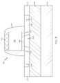
- Silicide areas 432 , 434 are formed for contacts on the source/drain regions 324 , 326 of the FET, as shown in FIG. 4 .
- a metal is deposited on top of the source/drain regions 324 , 326 .
- An anneal is then performed to form silicide, and then the metal is selectively removed.
- the metal can be nickel, cobalt, titanium, platinum, or an alloy or combination thereof.
- a disposable material layer 536 is formed over and in contact with the STI structures 210 , 212 , any portion of the semiconductor layer 106 (if any) between the silicide areas 432 , 434 and the spacer 322 , and the silicide areas 432 , 434 .
- the disposable material layer 536 in one embodiment, also contacts the sidewall 538 of the spacer 322 .
- the disposable material layer 536 comprises a thickness or height protects the silicide areas from subsequent etching of the hard mask 320 formed on the replacement gate 314 and a subsequent implantation of germanium into the replacement gate 314 .
- the disposable material layer 536 can comprise a thickness of greater than 200 A and less than the height of the gate.
- the disposable material layer 536 comprises a self-planarizing material such as flowable oxide (FOX) or a spin-on glass, or can comprise a non-self-planarizing material.
- the disposable material layer 536 can be deposited by spin-on coating of a self-planarizing material.
- the disposable material layer 536 can be formed by deposition of a disposable material by chemical vapor deposition, planarization of the deposited disposable material, for example, by chemical mechanical planarization (CMP), and by recessing the top surface of the planarized disposable material, for example, by a recess etch, which can be a wet etch or a dry etch.
- CMP chemical mechanical planarization
- a controlled etching process can be performed to remove the hard mask 320 and a portion of the spacer 322 .
- the etching of the spacer 322 can stop at or below a top surface of the polysilicon layer 318 .
- the etching process is a selective reactive ion etching (RIE) process that is selective to the material of the hard mask 320 and the spacer 322 , and does not remove portions of the polysilicon layer 318 .
- germanium atoms are implanted in an upper/top portion 640 of the exposed polysilicon layer 318 of the replacement gate 314 by ion implantation in a direction indicated by arrows 642 , as shown in FIG. 6 .
- the germanium implantation process uses germanium atoms at a high dose (>10 15 Ge atoms/cm 2 ) and at a low energy (i.e., an energy level where the germanium atoms only penetrate through a top portion 640 of the polysilicon layer of the replacement gate 314 and not into a lower/bottom portion 644 ).
- the directions 642 can be vertical or tilted between, for example, 5 and 45 degrees from vertical. Other angles are applicable as well.
- the top portion 640 of the polysilicon layer 318 expands laterally, as shown in FIG. 7 .
- a width 746 of the top portion 640 is greater than a width 748 of the bottom portion 644 of the polysilicon layer 318 , as shown in FIG. 7 .
- the top portion 640 of the polysilicon layer 318 is expanded laterally at least 10%.
- the width 746 is at least 110% of the width 748 .
- an upper region 750 of the top portion 640 of the polysilicon layer 318 extends above and over a top surface 752 of the spacer 322 .
- the top portion 640 of the polysilicon layer 318 comprises angles sidewalls, whereas the bottom portion 644 of the of the polysilicon layer comprises vertical sidewalls.
- the expanded areas improve gap fill during a subsequent RMG process.
- the funnel shape of the empty gate allows the Work function metal (WFM) and bulk metal (such as Al and W) the fill gate gap easier. Otherwise, if gate top opening is small and pinched-off the metal cannot fill into the gate forms voids.
- WFM Work function metal
- bulk metal such as Al and W
- a contact etch-stop liner 854 is formed over the structure, as shown in FIG. 8 .
- a contact etch-stop liner 854 is formed over and in contact with the STI structures 210 , 212 , any exposed portions of the semiconductor layer 106 between the STI structures 210 , 212 and the silicide areas 432 , 434 , any exposed portions of the semiconductor layer 106 between the silicide areas 432 , 434 and the spacer 322 , the silicide areas 432 , 434 , and a portion of the replacement gate structure 314 (the nitride spacer 322 and portion 750 of the polysilicon layer 318 implanted with Ge atoms that extends above the top surface 752 of the spacer 322 ).
- the contact etch-stop liner 854 comprises, for example, nitride, and can be formed using any conventional deposition process such as, for example,
- a dielectric layer 856 (e.g., an oxide layer, nitride layer, low-k material or any suitable combination of those materials) is formed over the entire structure. This dielectric layer 856 is then etched down to the level of the top surface of the gate spacer 322 , as shown in FIG. 9 . This process removes the portion 750 of the polysilicon layer 318 that extends above the top surface 752 of the spacer 322 , and the corresponding portion of the contact etch-stop liner 854 .
- the replacement gate 318 , 316 is removed via selective etching or another technique to form a gate cavity 1058 that exposes a portion 1060 of the high-k dielectric layer 316 or a portion of the semiconductor layer 106 if the high-k dielectric have not been formed, as shown in FIG. 10 .
- the gate cavity 1058 comprises a top portion 1062 that has been laterally expanded as a result of the lateral expansion of the polysilicon layer 318 .
- a width 1064 of the top portion 1062 of the cavity 1058 is greater than a width 1066 of the bottom portion 1068 of the cavity 1058 , both of which correspond to the top and bottom portions 640 , 642 of the polysilicon layer 318 that has been removed.
- the top portion 512 of the gate cavity layer is expanded laterally at least 10%.
- the width 1064 is at least 110% of the width 1066 .
- the top portion 1062 of the gate cavity 1058 comprises angled sidewalls, whereas the bottom portion 1068 of the gate cavity 1058 comprises vertical sidewalls.
- a high-k dielectric material is blanket deposited, for example by CVD (chemical vapor deposition), PECVD (plasma enhanced chemical vapor deposition), or ALD (Atomic layer deposition).
- CVD chemical vapor deposition
- PECVD plasma enhanced chemical vapor deposition
- ALD Atomic layer deposition
- the excessive high-k gate dielectric above the dielectric layer 856 can be removed, for example, by polishing such as chemically mechanical polishing (CMP) and/or etching to form a high-k gate dielectric layer 1170 on and in contact with the dielectric layer 316 (if formed), the vertical sidewalls 1172 of the spacer 322 , and the angled sidewalls 1174 of the spacer 322 .
- CMP chemically mechanical polishing
- high-k materials include but are not limited to metal oxides such as hafnium oxide, hafnium silicon oxide, hafnium silicon oxynitride, lanthanum oxide, lanthanum aluminum oxide, zirconium oxide, zirconium silicon oxide, zirconium silicon oxynitride, tantalum oxide, titanium oxide, barium strontium titanium oxide, barium titanium oxide, strontium titanium oxide, yttrium oxide, aluminum oxide, lead scandium tantalum oxide, and lead zinc niobate.
- the high-k may further include dopants such as lanthanum, aluminum.
- the conductive material comprises polycrystalline or amorphous silicon, germanium, silicon germanium, a metal (e.g., tungsten, titanium, tantalum, ruthenium, zirconium, cobalt, copper, aluminum, lead, platinum, tin, silver, gold), a conducting metallic compound material (e.g., tantalum nitride, titanium nitride, tungsten silicide, tungsten nitride, ruthenium oxide, cobalt silicide, nickel silicide), carbon nanotube, conductive carbon, or any suitable combination of these materials.
- a metal e.g., tungsten, titanium, tantalum, ruthenium, zirconium, cobalt, copper, aluminum, lead, platinum, tin, silver, gold
- a conducting metallic compound material e.g., tantalum nitride, titanium nitride, tungsten silicide, tungsten nitride, ruthenium oxide, cobalt si
- the conductive material may further comprise dopants that are incorporated during or after deposition.
- the conductive material may comprises multiple layers such as gate work function setting layer 1178 (work function metal) and gate conductive layer.
- the dielectric layer 1170 is not formed and the gate work function setting layer is formed on and in contact with the dielectric layer 316 (if formed), the vertical sidewalls 1172 of the spacer 322 , and the angled sidewalls 1174 of the spacer 322 .
- An optional barrier layer such as TiN can be inserted into the interface between the WFM 1178 and the high-k gate dielectric layer 1170 .
- Contacts (not shown) can then be formed for the silicide areas 432 and 434 .
- One or more processes can be used to form the contacts.
- FIGS. 1-11 show only one semiconductor device being fabricated, embodiments of the present disclosure are applicable to fabricating multiple semiconductor devices (e.g., multiple nFETs or pFETS and/or nFETs and pFETS). It should be also noted that embodiments of the present disclosure are not limited to the processes discussed above with respect to FIGS. 1-11 . Embodiments of the present disclosure are applicable to any semiconductor device and fabrication process that implements a replacement metal gate.
- FIG. 12 is an operational flow diagram illustrating one process for forming a semiconductor device with a replacement metal gate comprising an expanded upper portion according to one embodiment of the present invention.
- the operational flow diagram begins at step 1202 and flows directly to step 1204 . It should be noted that each of the steps shown in FIG. 12 has been discussed in greater detail above with respect to FIGS. 1-11 .
- a replacement gate structure, at step 1204 is formed on a semiconductor layer of a substrate.
- the replacement gate structure comprises at least a polysilicon layer.
- a gate spacer is formed on the replacement gate structure, at step 1206 .
- Atoms, at step 1208 are implanted in an upper portion of the polysilicon layer.
- the implanting expands the upper portion of the polysilicon layer and a corresponding upper portion of the gate spacer in at least a lateral direction beyond a lower portion of the polysilicon layer and a lower portion of the gate spacer, respectively.
- the polysilicon layer is removed to form a gate cavity surrounded by the gate spacer, at step 1210 .
- a metal gate stack, at step 1212 is formed within the gate cavity and in contact with sidewalls of the gate spacer.
- the metal gate stack comprises a upper portion having a width that is greater than a width of a lower portion of the metal gate stack. Additional fabrication processes such as contact formation can then be performed.
- the control flow exits at step 1214 .
Abstract
Description
Claims (20)
Priority Applications (1)
| Application Number | Priority Date | Filing Date | Title |
|---|---|---|---|
| US15/856,518 US10229984B2 (en) | 2015-12-18 | 2017-12-28 | Gap fill of metal stack in replacement gate process |
Applications Claiming Priority (3)
| Application Number | Priority Date | Filing Date | Title |
|---|---|---|---|
| US14/973,780 US9748358B2 (en) | 2015-12-18 | 2015-12-18 | Gap fill of metal stack in replacement gate process |
| US15/372,519 US9935174B2 (en) | 2015-12-18 | 2016-12-08 | Gap fill of metal stack in replacement gate process |
| US15/856,518 US10229984B2 (en) | 2015-12-18 | 2017-12-28 | Gap fill of metal stack in replacement gate process |
Related Parent Applications (1)
| Application Number | Title | Priority Date | Filing Date |
|---|---|---|---|
| US15/372,519 Continuation US9935174B2 (en) | 2015-12-18 | 2016-12-08 | Gap fill of metal stack in replacement gate process |
Publications (2)
| Publication Number | Publication Date |
|---|---|
| US20180122920A1 US20180122920A1 (en) | 2018-05-03 |
| US10229984B2 true US10229984B2 (en) | 2019-03-12 |
Family
ID=59066389
Family Applications (3)
| Application Number | Title | Priority Date | Filing Date |
|---|---|---|---|
| US14/973,780 Active US9748358B2 (en) | 2015-12-18 | 2015-12-18 | Gap fill of metal stack in replacement gate process |
| US15/372,519 Active US9935174B2 (en) | 2015-12-18 | 2016-12-08 | Gap fill of metal stack in replacement gate process |
| US15/856,518 Active US10229984B2 (en) | 2015-12-18 | 2017-12-28 | Gap fill of metal stack in replacement gate process |
Family Applications Before (2)
| Application Number | Title | Priority Date | Filing Date |
|---|---|---|---|
| US14/973,780 Active US9748358B2 (en) | 2015-12-18 | 2015-12-18 | Gap fill of metal stack in replacement gate process |
| US15/372,519 Active US9935174B2 (en) | 2015-12-18 | 2016-12-08 | Gap fill of metal stack in replacement gate process |
Country Status (1)
| Country | Link |
|---|---|
| US (3) | US9748358B2 (en) |
Families Citing this family (3)
| Publication number | Priority date | Publication date | Assignee | Title |
|---|---|---|---|---|
| US9167438B2 (en) | 2012-08-31 | 2015-10-20 | International Business Machines Corporation | Mobility detection for edge applications in wireless communication networks |
| CN110060987B (en) * | 2014-06-18 | 2021-03-12 | 艾克斯展示公司技术有限公司 | Micro-assembly LED display |
| US9748358B2 (en) * | 2015-12-18 | 2017-08-29 | International Business Machines Corporation | Gap fill of metal stack in replacement gate process |
Citations (10)
| Publication number | Priority date | Publication date | Assignee | Title |
|---|---|---|---|---|
| US20040043549A1 (en) | 2002-09-04 | 2004-03-04 | Renesas Technology Corp. | Method of manufacturing semiconductor device having gate electrode with expanded upper portion |
| US6905976B2 (en) | 2003-05-06 | 2005-06-14 | International Business Machines Corporation | Structure and method of forming a notched gate field effect transistor |
| US20080296707A1 (en) | 2006-01-11 | 2008-12-04 | Brent Alan Anderson | Semiconductor transistors with expanded top portions of gates |
| US7517746B2 (en) | 2007-04-24 | 2009-04-14 | United Microelectronics Corp. | Metal oxide semiconductor transistor with Y shape metal gate and fabricating method thereof |
| US7883950B2 (en) | 2006-11-29 | 2011-02-08 | Dongbu Hitek Co., Ltd. | Semiconductor device having reduced polysilicon pattern width and method of manufacturing the same |
| US7993997B2 (en) | 2007-10-01 | 2011-08-09 | Globalfoundries Singapore Pte. Ltd. | Poly profile engineering to modulate spacer induced stress for device enhancement |
| US8264048B2 (en) | 2008-02-15 | 2012-09-11 | Intel Corporation | Multi-gate device having a T-shaped gate structure |
| US8519454B2 (en) | 2011-03-30 | 2013-08-27 | International Business Machines Corporation | Structure and process for metal fill in replacement metal gate integration |
| US9048254B2 (en) | 2009-12-02 | 2015-06-02 | United Microelectronics Corp. | Semiconductor structure having a metal gate with side wall spacers |
| US9748358B2 (en) * | 2015-12-18 | 2017-08-29 | International Business Machines Corporation | Gap fill of metal stack in replacement gate process |
Family Cites Families (2)
| Publication number | Priority date | Publication date | Assignee | Title |
|---|---|---|---|---|
| US6436747B1 (en) * | 1999-04-21 | 2002-08-20 | Matsushita Electtric Industrial Co., Ltd. | Method of fabricating semiconductor device |
| KR100574338B1 (en) * | 2004-01-19 | 2006-04-26 | 삼성전자주식회사 | Method for forming metal gate in semiconductor device |
-
2015
- 2015-12-18 US US14/973,780 patent/US9748358B2/en active Active
-
2016
- 2016-12-08 US US15/372,519 patent/US9935174B2/en active Active
-
2017
- 2017-12-28 US US15/856,518 patent/US10229984B2/en active Active
Patent Citations (13)
| Publication number | Priority date | Publication date | Assignee | Title |
|---|---|---|---|---|
| US6835610B2 (en) | 2002-09-04 | 2004-12-28 | Renesas Technology Corp. | Method of manufacturing semiconductor device having gate electrode with expanded upper portion |
| US20040043549A1 (en) | 2002-09-04 | 2004-03-04 | Renesas Technology Corp. | Method of manufacturing semiconductor device having gate electrode with expanded upper portion |
| US6905976B2 (en) | 2003-05-06 | 2005-06-14 | International Business Machines Corporation | Structure and method of forming a notched gate field effect transistor |
| US8466503B2 (en) | 2006-01-11 | 2013-06-18 | International Business Machines Corporation | Semiconductor transistors with expanded top portions of gates |
| US20080296707A1 (en) | 2006-01-11 | 2008-12-04 | Brent Alan Anderson | Semiconductor transistors with expanded top portions of gates |
| US8753929B2 (en) | 2006-01-11 | 2014-06-17 | International Business Machines Corporation | Structure fabrication method |
| US7883950B2 (en) | 2006-11-29 | 2011-02-08 | Dongbu Hitek Co., Ltd. | Semiconductor device having reduced polysilicon pattern width and method of manufacturing the same |
| US7517746B2 (en) | 2007-04-24 | 2009-04-14 | United Microelectronics Corp. | Metal oxide semiconductor transistor with Y shape metal gate and fabricating method thereof |
| US7993997B2 (en) | 2007-10-01 | 2011-08-09 | Globalfoundries Singapore Pte. Ltd. | Poly profile engineering to modulate spacer induced stress for device enhancement |
| US8264048B2 (en) | 2008-02-15 | 2012-09-11 | Intel Corporation | Multi-gate device having a T-shaped gate structure |
| US9048254B2 (en) | 2009-12-02 | 2015-06-02 | United Microelectronics Corp. | Semiconductor structure having a metal gate with side wall spacers |
| US8519454B2 (en) | 2011-03-30 | 2013-08-27 | International Business Machines Corporation | Structure and process for metal fill in replacement metal gate integration |
| US9748358B2 (en) * | 2015-12-18 | 2017-08-29 | International Business Machines Corporation | Gap fill of metal stack in replacement gate process |
Non-Patent Citations (1)
| Title |
|---|
| List of IBM Patents or Patent Applications Treated as Related. |
Also Published As
| Publication number | Publication date |
|---|---|
| US20180122920A1 (en) | 2018-05-03 |
| US9748358B2 (en) | 2017-08-29 |
| US20170179256A1 (en) | 2017-06-22 |
| US9935174B2 (en) | 2018-04-03 |
| US20170179255A1 (en) | 2017-06-22 |
Similar Documents
| Publication | Publication Date | Title |
|---|---|---|
| US9059096B2 (en) | Method to form silicide contact in trenches | |
| US10164007B2 (en) | Transistor with improved air spacer | |
| KR101799636B1 (en) | Structure and method for finfet device | |
| US9917103B1 (en) | Diffusion break forming after source/drain forming and related IC structure | |
| US9748235B2 (en) | Gate stack for integrated circuit structure and method of forming same | |
| US10049985B2 (en) | Contact line having insulating spacer therein and method of forming same | |
| US7892911B2 (en) | Metal gate electrodes for replacement gate integration scheme | |
| US9018739B2 (en) | Semiconductor device and method of fabricating the same | |
| US20100038715A1 (en) | Thin body silicon-on-insulator transistor with borderless self-aligned contacts | |
| US10784363B2 (en) | Method and structure of forming finFET contact | |
| US9653602B1 (en) | Tensile and compressive fins for vertical field effect transistors | |
| US10229984B2 (en) | Gap fill of metal stack in replacement gate process | |
| US9048216B2 (en) | Self aligned embedded gate carbon transistors | |
| US20220359745A1 (en) | Semiconductor Device and Method | |
| US10224418B2 (en) | Integrated circuit fabrication with boron etch-stop layer | |
| US9595592B1 (en) | Forming dual contact silicide using metal multi-layer and ion beam mixing | |
| US20200343365A1 (en) | Gate Structure and Method | |
| US20130175632A1 (en) | Reduction of contact resistance and junction leakage | |
| US20220359654A1 (en) | Methods of Forming Semiconductor Devices Including Gate Barrier Layers | |
| US10985266B2 (en) | Method of gap filling for semiconductor device | |
| US9583397B1 (en) | Source/drain terminal contact and method of forming same | |
| US11798943B2 (en) | Transistor source/drain contacts and methods of forming the same | |
| US10546775B1 (en) | Field-effect transistors with improved dielectric gap fill | |
| CN115036360A (en) | Source/drain structure of semiconductor device and forming method thereof |
Legal Events
| Date | Code | Title | Description |
|---|---|---|---|
| AS | Assignment |
Owner name: INTERNATIONAL BUSINESS MACHINES CORPORATION, NEW Y Free format text: ASSIGNMENT OF ASSIGNORS INTEREST;ASSIGNORS:CHAN, VICTOR;HAN, JIN PING;KO, SHANGBIN;SIGNING DATES FROM 20151208 TO 20151210;REEL/FRAME:044499/0598 |
|
| FEPP | Fee payment procedure |
Free format text: ENTITY STATUS SET TO UNDISCOUNTED (ORIGINAL EVENT CODE: BIG.); ENTITY STATUS OF PATENT OWNER: LARGE ENTITY |
|
| STCF | Information on status: patent grant |
Free format text: PATENTED CASE |
|
| MAFP | Maintenance fee payment |
Free format text: PAYMENT OF MAINTENANCE FEE, 4TH YEAR, LARGE ENTITY (ORIGINAL EVENT CODE: M1551); ENTITY STATUS OF PATENT OWNER: LARGE ENTITY Year of fee payment: 4 |