US10229807B2 - Amplification of electromagnetic waves via interaction with an electron beam by using a waveguide having a linear interaction channel with curved parts and including rows of pillars extending through the waveguide - Google Patents
Amplification of electromagnetic waves via interaction with an electron beam by using a waveguide having a linear interaction channel with curved parts and including rows of pillars extending through the waveguide Download PDFInfo
- Publication number
- US10229807B2 US10229807B2 US15/519,018 US201515519018A US10229807B2 US 10229807 B2 US10229807 B2 US 10229807B2 US 201515519018 A US201515519018 A US 201515519018A US 10229807 B2 US10229807 B2 US 10229807B2
- Authority
- US
- United States
- Prior art keywords
- waveguide
- pillars
- section
- electron beam
- ghz
- Prior art date
- Legal status (The legal status is an assumption and is not a legal conclusion. Google has not performed a legal analysis and makes no representation as to the accuracy of the status listed.)
- Active
Links
- 230000003993 interaction Effects 0.000 title claims abstract description 30
- 238000010894 electron beam technology Methods 0.000 title claims abstract description 28
- 230000003321 amplification Effects 0.000 title claims abstract description 7
- 238000003199 nucleic acid amplification method Methods 0.000 title claims abstract description 7
- 229910052751 metal Inorganic materials 0.000 claims description 7
- 239000002184 metal Substances 0.000 claims description 7
- 238000004519 manufacturing process Methods 0.000 claims description 5
- 239000011800 void material Substances 0.000 claims description 3
- 230000005670 electromagnetic radiation Effects 0.000 description 8
- 230000008878 coupling Effects 0.000 description 5
- 238000010168 coupling process Methods 0.000 description 5
- 238000005859 coupling reaction Methods 0.000 description 5
- 239000000463 material Substances 0.000 description 5
- PCHJSUWPFVWCPO-UHFFFAOYSA-N gold Chemical compound [Au] PCHJSUWPFVWCPO-UHFFFAOYSA-N 0.000 description 4
- 239000010931 gold Substances 0.000 description 4
- 229910052737 gold Inorganic materials 0.000 description 4
- XUIMIQQOPSSXEZ-UHFFFAOYSA-N Silicon Chemical compound [Si] XUIMIQQOPSSXEZ-UHFFFAOYSA-N 0.000 description 3
- 229910052710 silicon Inorganic materials 0.000 description 3
- 239000010703 silicon Substances 0.000 description 3
- RYGMFSIKBFXOCR-UHFFFAOYSA-N Copper Chemical compound [Cu] RYGMFSIKBFXOCR-UHFFFAOYSA-N 0.000 description 2
- 239000010949 copper Substances 0.000 description 2
- 229910052802 copper Inorganic materials 0.000 description 2
- 238000000034 method Methods 0.000 description 2
- 230000005855 radiation Effects 0.000 description 2
- 239000000654 additive Substances 0.000 description 1
- 230000000996 additive effect Effects 0.000 description 1
- 230000004075 alteration Effects 0.000 description 1
- 239000004411 aluminium Substances 0.000 description 1
- 229910052782 aluminium Inorganic materials 0.000 description 1
- XAGFODPZIPBFFR-UHFFFAOYSA-N aluminium Chemical compound [Al] XAGFODPZIPBFFR-UHFFFAOYSA-N 0.000 description 1
- 238000005452 bending Methods 0.000 description 1
- 230000008901 benefit Effects 0.000 description 1
- 230000005540 biological transmission Effects 0.000 description 1
- 238000004891 communication Methods 0.000 description 1
- 238000010276 construction Methods 0.000 description 1
- 230000005672 electromagnetic field Effects 0.000 description 1
- 230000001747 exhibiting effect Effects 0.000 description 1
- 239000012212 insulator Substances 0.000 description 1
- 239000011159 matrix material Substances 0.000 description 1
- 150000002739 metals Chemical class 0.000 description 1
- 230000004048 modification Effects 0.000 description 1
- 238000012986 modification Methods 0.000 description 1
- 239000002245 particle Substances 0.000 description 1
- 230000008569 process Effects 0.000 description 1
- 230000001902 propagating effect Effects 0.000 description 1
- 238000005086 pumping Methods 0.000 description 1
- 238000007789 sealing Methods 0.000 description 1
- 238000001228 spectrum Methods 0.000 description 1
- 239000000758 substrate Substances 0.000 description 1
Images


Classifications
-
- H—ELECTRICITY
- H01—ELECTRIC ELEMENTS
- H01J—ELECTRIC DISCHARGE TUBES OR DISCHARGE LAMPS
- H01J23/00—Details of transit-time tubes of the types covered by group H01J25/00
- H01J23/16—Circuit elements, having distributed capacitance and inductance, structurally associated with the tube and interacting with the discharge
-
- H—ELECTRICITY
- H01—ELECTRIC ELEMENTS
- H01J—ELECTRIC DISCHARGE TUBES OR DISCHARGE LAMPS
- H01J25/00—Transit-time tubes, e.g. klystrons, travelling-wave tubes, magnetrons
- H01J25/34—Travelling-wave tubes; Tubes in which a travelling wave is simulated at spaced gaps
- H01J25/36—Tubes in which an electron stream interacts with a wave travelling along a delay line or equivalent sequence of impedance elements, and without magnet system producing an H-field crossing the E-field
-
- H—ELECTRICITY
- H01—ELECTRIC ELEMENTS
- H01J—ELECTRIC DISCHARGE TUBES OR DISCHARGE LAMPS
- H01J23/00—Details of transit-time tubes of the types covered by group H01J25/00
- H01J23/36—Coupling devices having distributed capacitance and inductance, structurally associated with the tube, for introducing or removing wave energy
-
- H—ELECTRICITY
- H01—ELECTRIC ELEMENTS
- H01J—ELECTRIC DISCHARGE TUBES OR DISCHARGE LAMPS
- H01J25/00—Transit-time tubes, e.g. klystrons, travelling-wave tubes, magnetrons
- H01J25/02—Tubes with electron stream modulated in velocity or density in a modulator zone and thereafter giving up energy in an inducing zone, the zones being associated with one or more resonators
-
- H—ELECTRICITY
- H01—ELECTRIC ELEMENTS
- H01P—WAVEGUIDES; RESONATORS, LINES, OR OTHER DEVICES OF THE WAVEGUIDE TYPE
- H01P3/00—Waveguides; Transmission lines of the waveguide type
- H01P3/12—Hollow waveguides
-
- H—ELECTRICITY
- H01—ELECTRIC ELEMENTS
- H01P—WAVEGUIDES; RESONATORS, LINES, OR OTHER DEVICES OF THE WAVEGUIDE TYPE
- H01P3/00—Waveguides; Transmission lines of the waveguide type
- H01P3/12—Hollow waveguides
- H01P3/123—Hollow waveguides with a complex or stepped cross-section, e.g. ridged or grooved waveguides
-
- H—ELECTRICITY
- H03—ELECTRONIC CIRCUITRY
- H03F—AMPLIFIERS
- H03F1/00—Details of amplifiers with only discharge tubes, only semiconductor devices or only unspecified devices as amplifying elements
- H03F1/02—Modifications of amplifiers to raise the efficiency, e.g. gliding Class A stages, use of an auxiliary oscillation
- H03F1/04—Modifications of amplifiers to raise the efficiency, e.g. gliding Class A stages, use of an auxiliary oscillation in discharge-tube amplifiers
- H03F1/06—Modifications of amplifiers to raise the efficiency, e.g. gliding Class A stages, use of an auxiliary oscillation in discharge-tube amplifiers to raise the efficiency of amplifying modulated radio frequency waves; to raise the efficiency of amplifiers acting also as modulators
-
- H—ELECTRICITY
- H03—ELECTRONIC CIRCUITRY
- H03F—AMPLIFIERS
- H03F3/00—Amplifiers with only discharge tubes or only semiconductor devices as amplifying elements
- H03F3/189—High-frequency amplifiers, e.g. radio frequency amplifiers
-
- H—ELECTRICITY
- H03—ELECTRONIC CIRCUITRY
- H03F—AMPLIFIERS
- H03F3/00—Amplifiers with only discharge tubes or only semiconductor devices as amplifying elements
- H03F3/54—Amplifiers using transit-time effect in tubes or semiconductor devices
-
- H—ELECTRICITY
- H03—ELECTRONIC CIRCUITRY
- H03F—AMPLIFIERS
- H03F3/00—Amplifiers with only discharge tubes or only semiconductor devices as amplifying elements
- H03F3/54—Amplifiers using transit-time effect in tubes or semiconductor devices
- H03F3/58—Amplifiers using transit-time effect in tubes or semiconductor devices using travelling-wave tubes
Definitions
- Embodiments of the invention relate to a rectangular waveguide providing amplification of an electromagnetic wave via interactions with an electron beam in a linear interaction channel.
- the present invention relates to a device able to operate as an amplifier or oscillator at gigahertz and terahertz frequencies with good gain and output power, and, more specifically, to a device whose physical design makes it straightforward to manufacture, disassemble and reassemble.
- TWT Travelling wave tubes
- Folded waveguides, staggered double grating waveguides and sine waveguides have all been demonstrated in terahertz TWTs, with cylindrical or sheet electron beams in the 100 to 850 GHz frequency range.
- Such waveguides have to be fabricated in two (or more) precision parts with the sealing edge critical to confinement of the propagating electromagnetic field.
- a very high precision assembly process is required (to eliminate misalignments that could perturb the wave propagation).
- New structures are desired with simpler assembly in order to lower the costs and improve repeatability and reliability.
- the present invention achieves superior performance by the use of curves. More specifically, the present invention provides required functions by a novel physical and electrical waveguide configuration. Embodiments may act as an amplifier or oscillator in the frequency band from 10 to 2,000 gigahertz. The present invention improves over previous devices in a number of significant areas, including gain, output power, ease of manufacture and ease of vacuum pumping.
- the present invention may be suitably applied to the construction and implementation of particle accelerators
- the present invention comprises a rectangular section waveguide providing amplification of an electromagnetic wave via interaction with an electron beam in a linear interaction channel, where the electron beam enters the waveguide at a first curved part of the waveguide, traverses the linear interaction channel and exits the waveguide at a second curved part of the waveguide.
- the interaction channel is defined by two parallel rows of pillars each attached substantially perpendicularly to the base of the waveguide.
- the rows of pillars extend around the first and second curves of the waveguide, into the linear sections of the waveguide.
- each pillar may be a void between the top of each pillar and the roof of the waveguide.
- the curve of the waveguide may be such that the base and top of the waveguide are planar.
- the top of the waveguide may be attached to complete manufacture and subsequently detached and re-attached.
- the pillars may be not attached to the walls of the waveguide. At least one pillar in each curved part of the waveguide may be modified in shape relative to other pillars.
- the present invention may operate in the 10 GHz to 2,000 GHz band, the 200 GHz to 1,000 GHz band, the 25 GHz to 250 GHz band and/or the 30 GHz to 40 GHz band
- the pillars may be substantially square or rectangular in section, or circular or elliptical or triangular in section.
- the present invention may comprise metal components and/or components coated in metal.
- FIG. 1 shows a plan view of an embodiment of the present invention.
- FIG. 2 shows a perspective view of part of an embodiment of the present invention.
- FIG. 3 shows a plan view of part of an embodiment of the present invention.
- FIG. 4 shows a chart of certain S-parameters for one embodiment of the present invention.
- FIG. 5A shows a cross-sectional view of a section of the device in which the lid is attached to each of the walls, in accordance with some embodiments of the present invention.
- FIG. 5B shows a cross-sectional view of a section of the device in which the lid is removed from the walls, in accordance with some embodiments of the present invention.
- FIG. 6A shows a plan view of circular or substantially circular pillars, in accordance with some embodiments of the present invention.
- FIG. 6B shows a plan view of elliptical or substantially elliptical pillars, in accordance with some embodiments of the present invention.
- FIG. 6C shows a plan view of triangular or substantially triangular pillars, in accordance with some embodiments of the present invention.
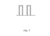
- FIG. 7 shows a side view of a pair of coated pillars, in accordance with some embodiments of the present invention.
- FIG. 1 shows a plan view of an embodiment of the present invention. The figure is not to scale.
- the present invention ( 10 ) consists of a waveguide. Electromagnetic radiation enters the device through a first microwave flange ( 41 ) and exits through a second microwave flange ( 51 ).
- the first flange ( 41 ) connects to a section of tapered waveguide ( 43 ) acting as a converter to a section of waveguide ( 11 ).
- This section of waveguide ( 11 ) connects to a first curved section ( 13 ) where an electron beam (not shown in FIG. 1 ) enters through a first beam tunnel ( 23 ).
- the electron beam and electromagnetic radiation interact within a further linear section of waveguide, the interaction section ( 15 ).
- the electron beam then exits via a second beam tunnel ( 25 ) at a second curved section ( 17 ).
- the electromagnetic radiation continues into a further linear section of waveguide ( 19 ), then into an inversely tapered section of waveguide ( 53 ) acting as a converter, and exits at the second microwave flange ( 51 ).
- pillars ( 21 ) are not attached to the walls.
- the pillars ( 21 ) are rectangular but in other embodiments there may be other shapes such as square, triangular ( FIG. 6C ), circular ( FIG. 6A ), or elliptical ( FIG. 6B ) pillars ( 21 ), or any cross-section adapted and/or optimised for a particular embodiment.
- Electromagnetic radiation and the electron beam interact in an interaction channel defined by the pillars ( 21 ) within the interaction section ( 15 ).
- FIG. 2 shows a perspective view of part of an embodiment of the present invention. The figure is not to scale.
- FIG. 2 shows a perspective view of a first operative section of an embodiment of the present invention ( 10 ).
- This comprises a first linear section of waveguide ( 11 ) with rectangular cross-section, connected to a first curved section of waveguide ( 13 ) with rectangular cross-section, connected to an interaction section of waveguide ( 15 ) with rectangular cross-section.
- Electromagnetic radiation enters the first section of waveguide ( 11 ) and proceeds towards the curve ( 13 ). At the curve ( 13 ) an electron beam (not shown in FIG. 2 ) is injected via a first beam tunnel ( 23 ). The electron beam and electromagnetic radiation interact along the interaction section of waveguide ( 15 )
- FIG. 5A shows a cross-sectional view (not to scale) of a section of the device ( 10 ) in which the lid or roof is in communication with each of the opposing walls
- FIG. 5B shows a cross-sectional view (not to scale) of a section of the device ( 10 ) in which the lid or roof is removed or detached from the walls.
- the design of the present invention minimises field strength where the lid and walls meet. Consequently a preferred mode of manufacture is to make the walls and base as a single component, attach the pillars ( 21 ) to the base, and then make a joint where the walls and lid meet, because this reduces the criticality of the joint.
- an electron beam passes between rows of pillars ( 21 ).
- the present invention supports a cylindrical electron beam , which is straightforward to focus and to generate (for example by well-established Pierce electron guns).
- FIG. 3 shows a plan view of part of an embodiment of the present invention. This figure is not to scale.
- FIG. 3 shows a plan view of a second operative section of an embodiment of the present invention ( 10 ). This comprises the interaction section of waveguide ( 15 ) with rectangular cross-section, connected to a second curved section of waveguide ( 17 ) with rectangular cross-section, connected to a third linear section of waveguide ( 19 ) with rectangular cross-section.
- Electromagnetic radiation and an electron beam ( 27 ) interact in the interaction section of waveguide ( 15 ).
- the electron beam ( 27 ) exits the waveguide ( 17 ) via a second beam tunnel ( 25 ), and the electromagnetic radiation passes around the curve ( 17 ) to enter the third linear section of waveguide ( 19 ).
- Certain pillars may differ in shape from the remainder of the pillars ( 21 ) in order to avoid intersecting the electron beam ( 27 ).
- one or more pillars ( 29 ) may have part of their cross-section removed where the pillars ( 29 ) would otherwise obstruct the electron beam ( 27 ).
- FIG. 1 shows only a simple embodiment (parallel rows of pillars having reduced height toward the first microwave flange ( 41 ) and the second microwave flange ( 51 )). Because the curves ( 13 and 17 ) separate the interaction section ( 15 ) from the coupling sections ( 11 and 19 ), the interaction section ( 15 ) and coupling sections ( 11 and 19 ) may be designed independently without any interacting constraints. Consequently further embodiments may be produced using a different geometry and/or taper. For example, in certain situations it may be envisaged that arranging the row of pillars to converge or diverge towards the walls could improve the performance.
- the radii of the curved sections ( 13 and 17 ) may be varied between embodiments in order to optimise performance according to the respective requirements.
- FIG. 1 shows ninety degree curves
- the degree of curvature of the curved sections ( 13 and 17 ) may be varied between embodiments in order to optimise performance according to the respective requirements.
- coupling sections of waveguide may be provided as is well known in the art, to allow entry and exit of the electromagnetic wave. Amplification is achieved by interaction of the electromagnetic wave and the electron beam ( 27 ) via the geometry of the waveguide and the pillars ( 21 and 29 , as shown in FIG. 3 ).
- the present invention may also be used as an oscillator in the well-known manner, by providing a coupling section (wave output; not shown) at one end only and providing no input signal.
- Components of the device ( 10 ) may be manufactured in any material with good electrical conductivity, or any suitable substrate coated with a material with good electrical conductivity.
- Suitable materials with good electrical conductivity include many metals for example aluminium, copper or gold.
- Components of the device ( 10 ) may be made in silicon coated with a conducting metal, for example gold.
- Components of the device ( 10 ) may be made in double silicon-on-insulator (a silicon layer coated with gold).
- FIG. 7 shows an illustrative embodiment of a pair of pillars that have been coated.
- the pillars can be manufactured of a first material (e.g., silicon) and coated with a material exhibiting good electrical conductivity (e.g., a metal, copper, gold, and so forth).
- a first material e.g., silicon
- a material exhibiting good electrical conductivity e.g., a metal, copper, gold, and so forth.
- Components of the device ( 10 ) may be made by additive or subtractive techniques.
- the device ( 10 ) In operation the device ( 10 ) is evacuated.
- the relative lack of internal structure in the present invention assists this function.
- This device may be tailored for operation at a range of frequencies in the band 10 GHz to 2,000 GHz.
- the device is designed for amplification in the 32 to 37 GHz frequency band.
- the dimensions of the device are as follows:
- FIG. 4 shows transmission parameters S11 and S21 as a function of the microwave frequency.
- the x-axis is the frequency in gigahertz from 29 GHz (left side of chart) to 40 GHz (right side of chart).
- the y-axis is the value of the S parameter in decibels (DB) from zero decibels (top of chart) to minus fifty decibels (bottom of chart).
- the solid line is S11 representing the reflected radiation
- the dashed line is S21 representing transmitted radiation.
- the S-parameters refer to the well-known scattering matrix model of a multiport waveguide device.
- the lower and the upper cut-off frequencies mainly depend on the internal width of the waveguide ( 15 ) and the height of the pillars ( 21 and 29 , as shown in FIG. 3 ) respectively.
- the phase velocity is mainly determined by the longitudinal spacing of the pillars ( 21 and 29 ), the internal width of the waveguide ( 15 ) and the height of the pillars ( 21 and 29 ). It is well known to those skilled in the art how changing these physical dimensions allows the device to be tailored to give a range of electromagnetic properties, including operation at other frequencies, and operating as an amplifier or an oscillator.
Landscapes
- Engineering & Computer Science (AREA)
- Power Engineering (AREA)
- Microwave Amplifiers (AREA)
- Particle Accelerators (AREA)
- Control Of Motors That Do Not Use Commutators (AREA)
Abstract
Description
-
- Internal width of interaction section (15)=3.45 mm
- Internal height of interaction section (15)=2.5 mm
- Length of interaction section (15)=115 mm
- Minimum radius of curvature for curves (13 and 17)=3.2 mm
- Degree of curvature at each curve (13 and 17)=90 degrees
- Pillar (21 and 29) height=1.4 mm
- Pillar (21 and 29) width, length=0.55 mm
- Pillar (21 and 29) longitudinal stepping (periodicity)=2.3 mm
- Pillar (21 and 29) transverse spacing=0.7 mm
- Number of pillars of the interaction section (15)=100 (i.e., 50 pairs)
- Electron beam (29) centre, below pillar top=0.15 mm
- Electron beam (29) radius=0.25 mm
- Electron beam (29) energy=13 keV
- Input microwave power=100 milliwatts
Claims (19)
Applications Claiming Priority (3)
| Application Number | Priority Date | Filing Date | Title |
|---|---|---|---|
| GBGB1418133.3A GB201418133D0 (en) | 2014-10-14 | 2014-10-14 | Waveguide |
| GB1418133.3 | 2014-10-14 | ||
| PCT/GB2015/052993 WO2016059388A1 (en) | 2014-10-14 | 2015-10-13 | Waveguide |
Publications (2)
| Publication Number | Publication Date |
|---|---|
| US20170230010A1 US20170230010A1 (en) | 2017-08-10 |
| US10229807B2 true US10229807B2 (en) | 2019-03-12 |
Family
ID=52001363
Family Applications (1)
| Application Number | Title | Priority Date | Filing Date |
|---|---|---|---|
| US15/519,018 Active US10229807B2 (en) | 2014-10-14 | 2015-10-13 | Amplification of electromagnetic waves via interaction with an electron beam by using a waveguide having a linear interaction channel with curved parts and including rows of pillars extending through the waveguide |
Country Status (3)
| Country | Link |
|---|---|
| US (1) | US10229807B2 (en) |
| GB (2) | GB201418133D0 (en) |
| WO (1) | WO2016059388A1 (en) |
Citations (4)
| Publication number | Priority date | Publication date | Assignee | Title |
|---|---|---|---|---|
| US2469964A (en) * | 1941-05-03 | 1949-05-10 | Bell Telephone Labor Inc | Electron discharge apparatus |
| US2708236A (en) * | 1950-03-18 | 1955-05-10 | Bell Telephone Labor Inc | Microwave amplifiers |
| US2959707A (en) * | 1958-03-03 | 1960-11-08 | Itt | Slow wave propagating structure |
| US4617493A (en) * | 1985-01-28 | 1986-10-14 | United States Of America As Represented By The Secretary Of The Navy | Collective interaction klystron |
Family Cites Families (3)
| Publication number | Priority date | Publication date | Assignee | Title |
|---|---|---|---|---|
| NL6516981A (en) * | 1960-04-01 | 1966-07-18 | ||
| GB1049409A (en) * | 1963-10-29 | 1966-11-30 | Litton Industries Inc | Improvements in or relating to crossed field travelling wave amplifiers |
| KR101720591B1 (en) * | 2010-10-04 | 2017-03-29 | 삼성전자주식회사 | Terahertz interaction circuit having ridged structure |
-
2014
- 2014-10-14 GB GBGB1418133.3A patent/GB201418133D0/en not_active Ceased
-
2015
- 2015-10-13 US US15/519,018 patent/US10229807B2/en active Active
- 2015-10-13 WO PCT/GB2015/052993 patent/WO2016059388A1/en not_active Ceased
- 2015-10-13 GB GB1706546.7A patent/GB2547139B/en active Active
Patent Citations (4)
| Publication number | Priority date | Publication date | Assignee | Title |
|---|---|---|---|---|
| US2469964A (en) * | 1941-05-03 | 1949-05-10 | Bell Telephone Labor Inc | Electron discharge apparatus |
| US2708236A (en) * | 1950-03-18 | 1955-05-10 | Bell Telephone Labor Inc | Microwave amplifiers |
| US2959707A (en) * | 1958-03-03 | 1960-11-08 | Itt | Slow wave propagating structure |
| US4617493A (en) * | 1985-01-28 | 1986-10-14 | United States Of America As Represented By The Secretary Of The Navy | Collective interaction klystron |
Also Published As
| Publication number | Publication date |
|---|---|
| GB201706546D0 (en) | 2017-06-07 |
| WO2016059388A1 (en) | 2016-04-21 |
| GB2547139A (en) | 2017-08-09 |
| GB2547139B (en) | 2020-06-17 |
| GB201418133D0 (en) | 2014-11-26 |
| US20170230010A1 (en) | 2017-08-10 |
Similar Documents
| Publication | Publication Date | Title |
|---|---|---|
| US7952287B2 (en) | Traveling-wave tube 2D slow wave circuit | |
| US9406477B2 (en) | Traveling wave tube loaded by a material having negative permittivity and positive permeability | |
| CN113113278B (en) | Similar-trapezoid staggered double-gate slow wave structure | |
| Gee et al. | Gain analysis of higher-order-mode amplification in a dielectric-implanted multi-beam traveling wave structure | |
| Shi et al. | Study of 220 GHz dual-beam overmoded photonic crystal-loaded folded waveguide TWT | |
| Na et al. | Analysis of a broadband Q band folded waveguide traveling-wave tube | |
| CN105869971A (en) | Flap-topped sine waveguide slow wave structure | |
| Liao et al. | A rectangular groove-loaded folded waveguide for millimeter-wave traveling-wave tubes | |
| CN104051205B (en) | Coupling-input structure of gyro-traveling-wave tube | |
| Li et al. | A wideband high-voltage longitudinal output structure for Ka-band sheet beam traveling-wave tubes | |
| CN102054644B (en) | A waveguide slow-wave structure | |
| JP4453696B2 (en) | Waveguide-high frequency line converter and wireless communication device | |
| US10229807B2 (en) | Amplification of electromagnetic waves via interaction with an electron beam by using a waveguide having a linear interaction channel with curved parts and including rows of pillars extending through the waveguide | |
| US20160284502A1 (en) | Waveguide | |
| CN114783847A (en) | Novel slow wave structure based on staggered double-gate and zigzag waveguide | |
| CN115547789A (en) | Slow wave circuit, electromagnetic wave processing method and related equipment | |
| CN106128914B (en) | A kind of novel gyrotron traveling wave tube input coupler | |
| CN113161216B (en) | A Compact Dual Confocal Waveguide Gyroscopic Traveling Wave Tube Input Coupler | |
| KR102266009B1 (en) | Electromagnetic wave interaction circuit using sine-shaped waveguide | |
| Saavedra-Melo et al. | Wideband Glide-Symmetric Double Corrugated Gap Waveguide Traveling-Wave Tube for Millimeter-waves | |
| CN203895575U (en) | Low-order whispering gallery mode waveguide radiator | |
| Torgashov et al. | Multiple-Tunnel Meander-Line Slow-Wave Structure for a High-Power Millimeter-Band Traveling-Wave Tube | |
| Lu et al. | Optimized design of a Ka-band gyro-TWA based on axis-encircling electron beam | |
| CN116313701B (en) | A mode suppression device for a gyroscopic traveling wave tube | |
| Liu et al. | V-shape folded rectangular groove waveguide for millimeter-wave traveling-wave tube |
Legal Events
| Date | Code | Title | Description |
|---|---|---|---|
| AS | Assignment |
Owner name: LANCASTER UNIVERSITY BUSINESS ENTERPRISES LIMITED, Free format text: ASSIGNMENT OF ASSIGNORS INTEREST;ASSIGNOR:UNIVERSITY OF LANCASTER;REEL/FRAME:042042/0032 Effective date: 20151015 Owner name: UNIVERSITY OF LANCASTER, GREAT BRITAIN Free format text: ASSIGNMENT OF ASSIGNORS INTEREST;ASSIGNORS:PAOLONI, CLAUDIO;MINEO, MAURO;REEL/FRAME:042042/0018 Effective date: 20141014 |
|
| STCF | Information on status: patent grant |
Free format text: PATENTED CASE |
|
| MAFP | Maintenance fee payment |
Free format text: PAYMENT OF MAINTENANCE FEE, 4TH YR, SMALL ENTITY (ORIGINAL EVENT CODE: M2551); ENTITY STATUS OF PATENT OWNER: SMALL ENTITY Year of fee payment: 4 |
|
| AS | Assignment |
Owner name: UNIVERSITY OF LANCASTER, UNITED KINGDOM Free format text: ASSIGNMENT OF ASSIGNORS INTEREST;ASSIGNOR:LANCASTER UNIVERSITY BUSINESS ENTERPRISES LIMITED;REEL/FRAME:066511/0123 Effective date: 20231218 |