US10228328B2 - Organic electro-luminescent element and bioinstrumentation device - Google Patents
Organic electro-luminescent element and bioinstrumentation device Download PDFInfo
- Publication number
- US10228328B2 US10228328B2 US15/823,599 US201715823599A US10228328B2 US 10228328 B2 US10228328 B2 US 10228328B2 US 201715823599 A US201715823599 A US 201715823599A US 10228328 B2 US10228328 B2 US 10228328B2
- Authority
- US
- United States
- Prior art keywords
- luminescent
- delayed fluorescent
- fluorescent material
- organic electro
- element according
- Prior art date
- Legal status (The legal status is an assumption and is not a legal conclusion. Google has not performed a legal analysis and makes no representation as to the accuracy of the status listed.)
- Active
Links
- 0 *O[Al]1OC2=C3C(=C([5*])C([6*])=C2[7*])/C([4*])=C([3*])\C([2*])=N/31.C1=CC(C2=CC=CC(N3C4=C(C=CC=C4)C4=C3C=CC=C4)=C2)=CC(N2C3=C(C=CC=C3)C3=C2C=CC=C3)=C1.C1=CC2=C(C=C1)N(C1=CC(N3C4=C(C=CC=C4)C4=C3C=CC=C4)=CC(N3C4=C(C=CC=C4)C4=C3C=CC=C4)=C1)C1=C2C=CC=C1.C1=CC=C2C(=C1)C1=C(C=CC=C1)N2C1=CC=C(C2=CC=C(N3C4=C(C=CC=C4)C4=C3C=CC=C4)C=C2)C=C1.C1=CC=C2C(=C1)C1=C(C=CC=C1)N2C1=CC=CC(N2C3=C(C=CC=C3)C3=C2C=CC=C3)=C1.C1=CC=C2C(=C1)C1=C(C=CC=C1)N2CC1=CC=C(CN2C3=C(C=CC=C3)C3=C2C=CC=C3)C=C1.CC1=CC(N2C3=C(C=CC=C3)C3=C2C=CC=C3)=CC=C1C1=C(C)C=C(N2C3=CC=CC=C3C3=C2C=CC=C3)C=C1.[2*]C1=N2C3=C(O[Al]2O[Al]2OC4=C5C(=C([5*])C([6*])=C4[7*])/C([4*])=C([3*])\C([2*])=N/52)/C([7*])=C([6*])\C([5*])=C/3C([4*])=C1[3*] Chemical compound *O[Al]1OC2=C3C(=C([5*])C([6*])=C2[7*])/C([4*])=C([3*])\C([2*])=N/31.C1=CC(C2=CC=CC(N3C4=C(C=CC=C4)C4=C3C=CC=C4)=C2)=CC(N2C3=C(C=CC=C3)C3=C2C=CC=C3)=C1.C1=CC2=C(C=C1)N(C1=CC(N3C4=C(C=CC=C4)C4=C3C=CC=C4)=CC(N3C4=C(C=CC=C4)C4=C3C=CC=C4)=C1)C1=C2C=CC=C1.C1=CC=C2C(=C1)C1=C(C=CC=C1)N2C1=CC=C(C2=CC=C(N3C4=C(C=CC=C4)C4=C3C=CC=C4)C=C2)C=C1.C1=CC=C2C(=C1)C1=C(C=CC=C1)N2C1=CC=CC(N2C3=C(C=CC=C3)C3=C2C=CC=C3)=C1.C1=CC=C2C(=C1)C1=C(C=CC=C1)N2CC1=CC=C(CN2C3=C(C=CC=C3)C3=C2C=CC=C3)C=C1.CC1=CC(N2C3=C(C=CC=C3)C3=C2C=CC=C3)=CC=C1C1=C(C)C=C(N2C3=CC=CC=C3C3=C2C=CC=C3)C=C1.[2*]C1=N2C3=C(O[Al]2O[Al]2OC4=C5C(=C([5*])C([6*])=C4[7*])/C([4*])=C([3*])\C([2*])=N/52)/C([7*])=C([6*])\C([5*])=C/3C([4*])=C1[3*] 0.000 description 11
- BMXCHBVQGFGKGE-KGKMWPATSA-N C#CCN1C2=CC=C(/C=C/C3=[N+]4C(=C(C5=CC=C(I)C=C5)C5=C(C)C(C)=C(/C=C/C6=CC7=C(C=C6)N(CC#C)C6=C7C=CC=C6)N5[B-]4(F)F)C(C)=C3C)C=C2C2=C1C=CC=C2.IC1=CC=C(/N=C/C2=CC=CC(/C=N/C3=CC=C(I)C=C3)=C2)C=C1.[C-]#[N+]/C(C#N)=C1\C(/C=C2\C=CN(CCCCCCCCCCCC)C3=C2C=CC(C)=C3)=C([O-])\C1=C/C1=CC=[N+](CCCCCCCCCCCC)C2=C1C=CC(C)=C2 Chemical compound C#CCN1C2=CC=C(/C=C/C3=[N+]4C(=C(C5=CC=C(I)C=C5)C5=C(C)C(C)=C(/C=C/C6=CC7=C(C=C6)N(CC#C)C6=C7C=CC=C6)N5[B-]4(F)F)C(C)=C3C)C=C2C2=C1C=CC=C2.IC1=CC=C(/N=C/C2=CC=CC(/C=N/C3=CC=C(I)C=C3)=C2)C=C1.[C-]#[N+]/C(C#N)=C1\C(/C=C2\C=CN(CCCCCCCCCCCC)C3=C2C=CC(C)=C3)=C([O-])\C1=C/C1=CC=[N+](CCCCCCCCCCCC)C2=C1C=CC(C)=C2 BMXCHBVQGFGKGE-KGKMWPATSA-N 0.000 description 1
- MPLJETRVQJLOMH-UHFFFAOYSA-N C1=CC(N2C3=C(C=CC=C3)C3=C2C=CC=C3)=NC(N2C3=C(C=CC=C3)C3=C2C=CC=C3)=C1.CC1=CC=C(N(C2=CC=C(C)C=C2)C2=CC=C(C=CC3=CC=C(C=CC4=CC=C(N(C5=CC=C(C)C=C5)C5=CC=C(C)C=C5)C=C4)C=C3)C=C2)C=C1 Chemical compound C1=CC(N2C3=C(C=CC=C3)C3=C2C=CC=C3)=NC(N2C3=C(C=CC=C3)C3=C2C=CC=C3)=C1.CC1=CC=C(N(C2=CC=C(C)C=C2)C2=CC=C(C=CC3=CC=C(C=CC4=CC=C(N(C5=CC=C(C)C=C5)C5=CC=C(C)C=C5)C=C4)C=C3)C=C2)C=C1 MPLJETRVQJLOMH-UHFFFAOYSA-N 0.000 description 1
- OONXJEYLERCKPW-UHFFFAOYSA-N C1=CC2=C(C=C1)C1=C(N=CC=N1)C1=C2C=CC=C1.C1=NC2=C(C=C3N=S=NC3=C2)N=C1.C1=NC2=CC3=N/S/N=C\3C=C2N=C1 Chemical compound C1=CC2=C(C=C1)C1=C(N=CC=N1)C1=C2C=CC=C1.C1=NC2=C(C=C3N=S=NC3=C2)N=C1.C1=NC2=CC3=N/S/N=C\3C=C2N=C1 OONXJEYLERCKPW-UHFFFAOYSA-N 0.000 description 1
- UHBSQCSVQGLNQX-UHFFFAOYSA-N C1=CC2=C(C=C1)C=C(C1=C3C=CC=CC3=C(C3=CC4=C(C=CC=C4)C=C3)C3=C1C=CC=C3)C=C2.C1=CC=C(C(=CC2=CC=C(C3=CC=C(C=C(C4=CC=CC=C4)C4=CC=CC=C4)C=C3)C=C2)C2=CC=CC=C2)C=C1.C1=CC=C(C(=CC2=CC=C3C(=C2)C2(C4=C(C=CC=C4)C4=C2C=CC=C4)/C2=C\C(C=C(C4=CC=CC=C4)C4=CC=CC=C4)=C/C=C\32)C2=CC=CC=C2)C=C1.C1=CC=C(C2=CC(C3=CC=CC=C3)=CC(C3=C4C=CC=CC4=C(C4=CC(C5=CC=CC=C5)=CC(C5=CC=CC=C5)=C4)C4=C3C=CC=C4)=C2)C=C1.C1=CC=C([Si](C2=CC=CC=C2)(C2=CC=CC=C2)C2=CC(N3C4=C(C=CC=C4)C4=C3C=CC=C4)=CC(N3C4=C(C=CC=C4)C4=C3C=CC=C4)=C2)C=C1.C1=CC=C([Si](C2=CC=CC=C2)(C2=CC=CC=C2)C2=CC=C([Si](C3=CC=CC=C3)(C3=CC=CC=C3)C3=CC=CC=C3)C=C2)C=C1.C1=CC=C([Si](C2=CC=CC=C2)(C2=CC=CC=C2)C2=CC=CC([Si](C3=CC=CC=C3)(C3=CC=CC=C3)C3=CC=CC=C3)=C2)C=C1.C1=CC=C2C(=C1)CC1=C(C=CC=C1)[Si]21C2=CC=CC=C2CC2=C1C=CC=C2 Chemical compound C1=CC2=C(C=C1)C=C(C1=C3C=CC=CC3=C(C3=CC4=C(C=CC=C4)C=C3)C3=C1C=CC=C3)C=C2.C1=CC=C(C(=CC2=CC=C(C3=CC=C(C=C(C4=CC=CC=C4)C4=CC=CC=C4)C=C3)C=C2)C2=CC=CC=C2)C=C1.C1=CC=C(C(=CC2=CC=C3C(=C2)C2(C4=C(C=CC=C4)C4=C2C=CC=C4)/C2=C\C(C=C(C4=CC=CC=C4)C4=CC=CC=C4)=C/C=C\32)C2=CC=CC=C2)C=C1.C1=CC=C(C2=CC(C3=CC=CC=C3)=CC(C3=C4C=CC=CC4=C(C4=CC(C5=CC=CC=C5)=CC(C5=CC=CC=C5)=C4)C4=C3C=CC=C4)=C2)C=C1.C1=CC=C([Si](C2=CC=CC=C2)(C2=CC=CC=C2)C2=CC(N3C4=C(C=CC=C4)C4=C3C=CC=C4)=CC(N3C4=C(C=CC=C4)C4=C3C=CC=C4)=C2)C=C1.C1=CC=C([Si](C2=CC=CC=C2)(C2=CC=CC=C2)C2=CC=C([Si](C3=CC=CC=C3)(C3=CC=CC=C3)C3=CC=CC=C3)C=C2)C=C1.C1=CC=C([Si](C2=CC=CC=C2)(C2=CC=CC=C2)C2=CC=CC([Si](C3=CC=CC=C3)(C3=CC=CC=C3)C3=CC=CC=C3)=C2)C=C1.C1=CC=C2C(=C1)CC1=C(C=CC=C1)[Si]21C2=CC=CC=C2CC2=C1C=CC=C2 UHBSQCSVQGLNQX-UHFFFAOYSA-N 0.000 description 1
- DXGVWEAZMLCRCT-UHFFFAOYSA-N C1=CC2=C(C=C1)SC(C1=CC=C(N3C4=C(C=CC=C4)N(C4=CC=C(C5=NC6=C(C=CC=C6)S5)C=C4)C4=C3C=CC=C4)C=C1)=N2.C1=CC=C(C2=NC(C3=CC=CC=C3)=NC(C3=CC=C(N4C5=C(C=CC=C5)N(C5=CC=C(C6=NC(C7=CC=CC=C7)=NC(C7=CC=CC=C7)=N6)C=C5)C5=C4C=CC=C5)C=C3)=N2)C=C1.CC1=CC=C(C2=CC=C3C(=O)C4=C(C=CC(C5=CC=C(C)C=C5)=C4)C(=O)C3=C2)C=C1.CC1=CC=C2C(=O)C3=C(C=CC(C)=C3)C(=O)C2=C1.[C-]#[N+]C1=NC2=C(N=C1C#N)C1=C(C=C(C3=CC=C(N(C4=CC=CC=C4)C4=CC=CC=C4)C=C3)C=C1)C1=C2C=CC(C2=CC=C(N(C3=CC=CC=C3)C3=CC=CC=C3)C=C2)=C1 Chemical compound C1=CC2=C(C=C1)SC(C1=CC=C(N3C4=C(C=CC=C4)N(C4=CC=C(C5=NC6=C(C=CC=C6)S5)C=C4)C4=C3C=CC=C4)C=C1)=N2.C1=CC=C(C2=NC(C3=CC=CC=C3)=NC(C3=CC=C(N4C5=C(C=CC=C5)N(C5=CC=C(C6=NC(C7=CC=CC=C7)=NC(C7=CC=CC=C7)=N6)C=C5)C5=C4C=CC=C5)C=C3)=N2)C=C1.CC1=CC=C(C2=CC=C3C(=O)C4=C(C=CC(C5=CC=C(C)C=C5)=C4)C(=O)C3=C2)C=C1.CC1=CC=C2C(=O)C3=C(C=CC(C)=C3)C(=O)C2=C1.[C-]#[N+]C1=NC2=C(N=C1C#N)C1=C(C=C(C3=CC=C(N(C4=CC=CC=C4)C4=CC=CC=C4)C=C3)C=C1)C1=C2C=CC(C2=CC=C(N(C3=CC=CC=C3)C3=CC=CC=C3)C=C2)=C1 DXGVWEAZMLCRCT-UHFFFAOYSA-N 0.000 description 1
- RQCDMQPPMCTEOF-UHFFFAOYSA-N C1=CC=C(C(=CC2=CC3=C(C=C2)C2=C(C=C(C=C(C4=CC=CC=C4)C4=CC=CC=C4)C=C2)C32C3=C(C=CC(C=C(C4=CC=CC=C4)C4=CC=CC=C4)=C3)C3=C2/C=C(C=C(C2=CC=CC=C2)C2=CC=CC=C2)\C=C/3)C2=CC=CC=C2)C=C1.C1=CC=C(N(C2=CC=CC=C2)C2=CC3=C(C=C2)C2=C(C=C(N(C4=CC=CC=C4)C4=CC=CC=C4)C=C2)C32C3=C(C=CC(N(C4=CC=CC=C4)C4=CC=CC=C4)=C3)C3=C2/C=C(N(C2=CC=CC=C2)C2=CC=CC=C2)\C=C/3)C=C1.C1=CC=C2C(=C1)C1=C(C=CC=C1)N2C1=CC2=C(C=C1)C1=C(C=C(N3C4=CC=CC=C4C4=C3C=CC=C4)C=C1)C21C2=C(C=CC(N3C4=CC=CC=C4C4=C3C=CC=C4)=C2)C2=C1/C=C(N1C3=CC=CC=C3C3=C1C=CC=C3)\C=C/2.CC(C)(C)C1=CC=C(C2=NN=C(C3=CC4=C(C=C3)C3=C(C=CC=C3)C43C4=C(C=CC=C4)C4=C3/C=C(C3=NN=C(C5=CC=C(C(C)(C)C)C=C5)O3)\C=C/4)O2)C=C1.COC1=CC=C(C2=CC=C(C3=CC4=C(C=C3)C3=C(C=C(C5=CC=C(C6=CC=C(CO)C=C6)C=C5)C=C3)C43C4=C(C=CC(C5=CC=C(C6=CC=C(OC)C=C6)C=C5)=C4)C4=C3/C=C(C3=CC=C(C5=CC=C(CO)C=C5)C=C3)\C=C/4)C=C2)C=C1 Chemical compound C1=CC=C(C(=CC2=CC3=C(C=C2)C2=C(C=C(C=C(C4=CC=CC=C4)C4=CC=CC=C4)C=C2)C32C3=C(C=CC(C=C(C4=CC=CC=C4)C4=CC=CC=C4)=C3)C3=C2/C=C(C=C(C2=CC=CC=C2)C2=CC=CC=C2)\C=C/3)C2=CC=CC=C2)C=C1.C1=CC=C(N(C2=CC=CC=C2)C2=CC3=C(C=C2)C2=C(C=C(N(C4=CC=CC=C4)C4=CC=CC=C4)C=C2)C32C3=C(C=CC(N(C4=CC=CC=C4)C4=CC=CC=C4)=C3)C3=C2/C=C(N(C2=CC=CC=C2)C2=CC=CC=C2)\C=C/3)C=C1.C1=CC=C2C(=C1)C1=C(C=CC=C1)N2C1=CC2=C(C=C1)C1=C(C=C(N3C4=CC=CC=C4C4=C3C=CC=C4)C=C1)C21C2=C(C=CC(N3C4=CC=CC=C4C4=C3C=CC=C4)=C2)C2=C1/C=C(N1C3=CC=CC=C3C3=C1C=CC=C3)\C=C/2.CC(C)(C)C1=CC=C(C2=NN=C(C3=CC4=C(C=C3)C3=C(C=CC=C3)C43C4=C(C=CC=C4)C4=C3/C=C(C3=NN=C(C5=CC=C(C(C)(C)C)C=C5)O3)\C=C/4)O2)C=C1.COC1=CC=C(C2=CC=C(C3=CC4=C(C=C3)C3=C(C=C(C5=CC=C(C6=CC=C(CO)C=C6)C=C5)C=C3)C43C4=C(C=CC(C5=CC=C(C6=CC=C(OC)C=C6)C=C5)=C4)C4=C3/C=C(C3=CC=C(C5=CC=C(CO)C=C5)C=C3)\C=C/4)C=C2)C=C1 RQCDMQPPMCTEOF-UHFFFAOYSA-N 0.000 description 1
- QJYUVGBPGIHKOW-UHFFFAOYSA-N C1=CC=C(N(C2=CC(N(C3=CC=CC=C3)C3=CC=CC4=C3C=CC=C4)=CC([Si](C3=CC=CC=C3)(C3=CC=CC=C3)C3=CC(N(C4=CC=CC=C4)C4=CC=CC5=C4C=CC=C5)=CC(N(C4=CC=CC=C4)C4=CC=CC5=C4C=CC=C5)=C3)=C2)C2=CC=CC3=C2C=CC=C3)C=C1.C1=CC=C(N(C2=CC=C(N3C4=C(C=CC=C4)C4=C3C=CC=C4)C=C2)C2=CC=C(N3C4=C(C=CC=C4)C4=C3C=CC=C4)C=C2)C=C1.C1=CC=C(N(C2=CC=CC=C2)C2=CC=C(C3=NC(C4=CC=C(N(C5=CC=CC=C5)C5=CC=CC=C5)C=C4)=NC(C4=CC=C(N(C5=CC=CC=C5)C5=CC=CC=C5)C=C4)=N3)C=C2)C=C1.C1=CC=C(N(C2=CC=CC=C2)C2=CC=C(C3=NN=C(C4=CC=C([Si](C5=CC=CC=C5)(C5=CC=CC=C5)C5=CC=CC=C5)C=C4)O3)C=C2)C=C1.C[Si]1(CC[Si]2(C)C(C3=CC=CC=C3)=C(C3=CC=CC=C3)C(C3=CC=CC=C3)=C2C2=CC=CC=C2)C(C2=CC=CC=C2)=C(C2=CC=CC=C2)C(C2=CC=CC=C2)=C1C1=CC=CC=C1 Chemical compound C1=CC=C(N(C2=CC(N(C3=CC=CC=C3)C3=CC=CC4=C3C=CC=C4)=CC([Si](C3=CC=CC=C3)(C3=CC=CC=C3)C3=CC(N(C4=CC=CC=C4)C4=CC=CC5=C4C=CC=C5)=CC(N(C4=CC=CC=C4)C4=CC=CC5=C4C=CC=C5)=C3)=C2)C2=CC=CC3=C2C=CC=C3)C=C1.C1=CC=C(N(C2=CC=C(N3C4=C(C=CC=C4)C4=C3C=CC=C4)C=C2)C2=CC=C(N3C4=C(C=CC=C4)C4=C3C=CC=C4)C=C2)C=C1.C1=CC=C(N(C2=CC=CC=C2)C2=CC=C(C3=NC(C4=CC=C(N(C5=CC=CC=C5)C5=CC=CC=C5)C=C4)=NC(C4=CC=C(N(C5=CC=CC=C5)C5=CC=CC=C5)C=C4)=N3)C=C2)C=C1.C1=CC=C(N(C2=CC=CC=C2)C2=CC=C(C3=NN=C(C4=CC=C([Si](C5=CC=CC=C5)(C5=CC=CC=C5)C5=CC=CC=C5)C=C4)O3)C=C2)C=C1.C[Si]1(CC[Si]2(C)C(C3=CC=CC=C3)=C(C3=CC=CC=C3)C(C3=CC=CC=C3)=C2C2=CC=CC=C2)C(C2=CC=CC=C2)=C(C2=CC=CC=C2)C(C2=CC=CC=C2)=C1C1=CC=CC=C1 QJYUVGBPGIHKOW-UHFFFAOYSA-N 0.000 description 1
- YBPYVNFSIFDUNK-UHFFFAOYSA-N C1=CC=C(N(C2=CC=C(C3=CC=C(N(C4=CC=CC=C4)C4=C5C=CC=CC5=C5C=CC=CC5=C4)C=C3)C=C2)C2=CC3=C(C=CC=C3)C3=C2C=CC=C3)C=C1.C1=CC=C(N(C2=CC=C(C3=CC=C(N(C4=CC=CC=C4)C4=CC5=C(C=CC=C5)C=C4)C=C3)C=C2)C2=CC=C3C=CC=CC3=C2)C=C1.CC(C)(C)C1=CC=C(C2=NC=C(C3=CC4=C(C=C3)C3=C(/C=C(C5=CN=C(C6=CC=C(C(C)(C)C)C=C6)N=C5)\C=C/3)C43C4=C(C=CC=C4)C4=C3C=CC=C4)C=N2)C=C1.CC(C)(C)C1=CC=C(C2=NN=C(C3=CC4=C(C=C3)C3=C(C=C(C5=CC=C(N(C6=CC=CC=C6)C6=CC=CC=C6)C=C5)C=C3)C43C4=C(C=CC(C5=CC=C(N(C6=CC=CC=C6)C6=CC=CC=C6)C=C5)=C4)C4=C3/C=C(C3=NN=C(C5=CC=C(C(C)(C)C)C=C5)O3)\C=C/4)O2)C=C1.CC1=CC=C(N(C2=CC=C(C)C=C2)C2=C3C=CC=CC3=C(C3=C4C=CC=CC4=C(N(C4=CC=C(C)C=C4)C4=CC=C(C)C=C4)C(C)=C3)C=C2C)C=C1.CC1=CC=C2C=CC=CC2=C1N(C1=CC=CC=C1)C1=CC=C(C2=CC=C(N(C3=CC=CC=C3)C3=C(C)C=CC4=C3C=CC=C4)C=C2)C=C1 Chemical compound C1=CC=C(N(C2=CC=C(C3=CC=C(N(C4=CC=CC=C4)C4=C5C=CC=CC5=C5C=CC=CC5=C4)C=C3)C=C2)C2=CC3=C(C=CC=C3)C3=C2C=CC=C3)C=C1.C1=CC=C(N(C2=CC=C(C3=CC=C(N(C4=CC=CC=C4)C4=CC5=C(C=CC=C5)C=C4)C=C3)C=C2)C2=CC=C3C=CC=CC3=C2)C=C1.CC(C)(C)C1=CC=C(C2=NC=C(C3=CC4=C(C=C3)C3=C(/C=C(C5=CN=C(C6=CC=C(C(C)(C)C)C=C6)N=C5)\C=C/3)C43C4=C(C=CC=C4)C4=C3C=CC=C4)C=N2)C=C1.CC(C)(C)C1=CC=C(C2=NN=C(C3=CC4=C(C=C3)C3=C(C=C(C5=CC=C(N(C6=CC=CC=C6)C6=CC=CC=C6)C=C5)C=C3)C43C4=C(C=CC(C5=CC=C(N(C6=CC=CC=C6)C6=CC=CC=C6)C=C5)=C4)C4=C3/C=C(C3=NN=C(C5=CC=C(C(C)(C)C)C=C5)O3)\C=C/4)O2)C=C1.CC1=CC=C(N(C2=CC=C(C)C=C2)C2=C3C=CC=CC3=C(C3=C4C=CC=CC4=C(N(C4=CC=C(C)C=C4)C4=CC=C(C)C=C4)C(C)=C3)C=C2C)C=C1.CC1=CC=C2C=CC=CC2=C1N(C1=CC=CC=C1)C1=CC=C(C2=CC=C(N(C3=CC=CC=C3)C3=C(C)C=CC4=C3C=CC=C4)C=C2)C=C1 YBPYVNFSIFDUNK-UHFFFAOYSA-N 0.000 description 1
Images


Classifications
-
- G—PHYSICS
- G01—MEASURING; TESTING
- G01N—INVESTIGATING OR ANALYSING MATERIALS BY DETERMINING THEIR CHEMICAL OR PHYSICAL PROPERTIES
- G01N21/00—Investigating or analysing materials by the use of optical means, i.e. using sub-millimetre waves, infrared, visible or ultraviolet light
- G01N21/62—Systems in which the material investigated is excited whereby it emits light or causes a change in wavelength of the incident light
- G01N21/63—Systems in which the material investigated is excited whereby it emits light or causes a change in wavelength of the incident light optically excited
- G01N21/64—Fluorescence; Phosphorescence
- G01N21/6486—Measuring fluorescence of biological material, e.g. DNA, RNA, cells
-
- H—ELECTRICITY
- H01—ELECTRIC ELEMENTS
- H01L—SEMICONDUCTOR DEVICES NOT COVERED BY CLASS H10
- H01L27/00—Devices consisting of a plurality of semiconductor or other solid-state components formed in or on a common substrate
- H01L27/15—Devices consisting of a plurality of semiconductor or other solid-state components formed in or on a common substrate including semiconductor components with at least one potential-jump barrier or surface barrier specially adapted for light emission
-
- H01L51/0034—
-
- H01L51/5004—
-
- H01L51/5012—
-
- H—ELECTRICITY
- H10—SEMICONDUCTOR DEVICES; ELECTRIC SOLID-STATE DEVICES NOT OTHERWISE PROVIDED FOR
- H10K—ORGANIC ELECTRIC SOLID-STATE DEVICES
- H10K50/00—Organic light-emitting devices
- H10K50/10—OLEDs or polymer light-emitting diodes [PLED]
- H10K50/11—OLEDs or polymer light-emitting diodes [PLED] characterised by the electroluminescent [EL] layers
-
- H—ELECTRICITY
- H10—SEMICONDUCTOR DEVICES; ELECTRIC SOLID-STATE DEVICES NOT OTHERWISE PROVIDED FOR
- H10K—ORGANIC ELECTRIC SOLID-STATE DEVICES
- H10K85/00—Organic materials used in the body or electrodes of devices covered by this subclass
- H10K85/10—Organic polymers or oligomers
-
- A—HUMAN NECESSITIES
- A61—MEDICAL OR VETERINARY SCIENCE; HYGIENE
- A61B—DIAGNOSIS; SURGERY; IDENTIFICATION
- A61B5/00—Measuring for diagnostic purposes; Identification of persons
- A61B5/0059—Measuring for diagnostic purposes; Identification of persons using light, e.g. diagnosis by transillumination, diascopy, fluorescence
-
- H01L2251/552—
-
- H01L51/0059—
-
- H01L51/0067—
-
- H01L51/0072—
-
- H—ELECTRICITY
- H10—SEMICONDUCTOR DEVICES; ELECTRIC SOLID-STATE DEVICES NOT OTHERWISE PROVIDED FOR
- H10K—ORGANIC ELECTRIC SOLID-STATE DEVICES
- H10K2101/00—Properties of the organic materials covered by group H10K85/00
- H10K2101/20—Delayed fluorescence emission
-
- H—ELECTRICITY
- H10—SEMICONDUCTOR DEVICES; ELECTRIC SOLID-STATE DEVICES NOT OTHERWISE PROVIDED FOR
- H10K—ORGANIC ELECTRIC SOLID-STATE DEVICES
- H10K2101/00—Properties of the organic materials covered by group H10K85/00
- H10K2101/30—Highest occupied molecular orbital [HOMO], lowest unoccupied molecular orbital [LUMO] or Fermi energy values
-
- H—ELECTRICITY
- H10—SEMICONDUCTOR DEVICES; ELECTRIC SOLID-STATE DEVICES NOT OTHERWISE PROVIDED FOR
- H10K—ORGANIC ELECTRIC SOLID-STATE DEVICES
- H10K2101/00—Properties of the organic materials covered by group H10K85/00
- H10K2101/40—Interrelation of parameters between multiple constituent active layers or sublayers, e.g. HOMO values in adjacent layers
-
- H—ELECTRICITY
- H10—SEMICONDUCTOR DEVICES; ELECTRIC SOLID-STATE DEVICES NOT OTHERWISE PROVIDED FOR
- H10K—ORGANIC ELECTRIC SOLID-STATE DEVICES
- H10K85/00—Organic materials used in the body or electrodes of devices covered by this subclass
- H10K85/60—Organic compounds having low molecular weight
- H10K85/631—Amine compounds having at least two aryl rest on at least one amine-nitrogen atom, e.g. triphenylamine
-
- H—ELECTRICITY
- H10—SEMICONDUCTOR DEVICES; ELECTRIC SOLID-STATE DEVICES NOT OTHERWISE PROVIDED FOR
- H10K—ORGANIC ELECTRIC SOLID-STATE DEVICES
- H10K85/00—Organic materials used in the body or electrodes of devices covered by this subclass
- H10K85/60—Organic compounds having low molecular weight
- H10K85/649—Aromatic compounds comprising a hetero atom
- H10K85/654—Aromatic compounds comprising a hetero atom comprising only nitrogen as heteroatom
-
- H—ELECTRICITY
- H10—SEMICONDUCTOR DEVICES; ELECTRIC SOLID-STATE DEVICES NOT OTHERWISE PROVIDED FOR
- H10K—ORGANIC ELECTRIC SOLID-STATE DEVICES
- H10K85/00—Organic materials used in the body or electrodes of devices covered by this subclass
- H10K85/60—Organic compounds having low molecular weight
- H10K85/649—Aromatic compounds comprising a hetero atom
- H10K85/657—Polycyclic condensed heteroaromatic hydrocarbons
- H10K85/6572—Polycyclic condensed heteroaromatic hydrocarbons comprising only nitrogen in the heteroaromatic polycondensed ring system, e.g. phenanthroline or carbazole
Definitions
- solid-state elements based on inorganic semiconductors have been commonly used.
- devices using solid-state elements have been widely used in the field of bioinstrumentation, solid-state elements have problems such as poor biocompatibility in a broad sense including design freedom and flexibility.
- organic electro-luminescent elements (hereinafter also referred to as “organic EL element”), which recently attract attention, may be used as luminescent elements to possibly solve the problem.
- organic EL elements are excellent in processability and design freedom due to material properties and manufacturing process, and furthermore, flexibility may also be imparted to organic EL elements by deposition on a plastic substrate.
- the organic EL elements that emit light in a near-infrared range for example, those described in Non Patent Literature 1 to 6 are known.
- Patent Literature 1 discloses that an organic EL element having a high luminous efficiency can be provided by using a delayed fluorescent material as assistant dopant, but, as a result of studies by the present inventors, it has been found difficult to manufacture organic EL elements that emit light in the near-infrared range applicable for use in bioinstrumentation based on the disclosure of Patent Literature 1. Furthermore, organic EL elements often have a plurality of maximal values of emission spectrum, and light emission in the visible light range (other than a near-infrared range) produces noise having a negative effect on the reliability of organism sensing, and is therefore undesirable.
- An object of the present invention is, therefore, to provide an organic EL element that emits light in a near-infrared range, is excellent in both the electric properties and the device life, with a sufficiently low luminescent intensity of the maximal values in the emission spectrum in the visible light range, or with no maximal values observed in the visible light range, and a bioinstrumentation device using the same.
- the near-infrared range may generally be understood to include a lower limit of approximately 700 nm and an upper limit of approximately 2500 nm.
- some embodiments of the present invention may be configured to operate in a near-infrared range of approximately 700 nm to 800 nm, or near the maximum luminescence values.
- the upper limit of the near-infrared range may be approximately 900 nm or approximately 1000 nm according to different example configurations.
- the present invention includes an organic EL element having a luminescence peak in a near-infrared range, comprising a positive electrode, a negative electrode, and at least one organic layer including a luminescent layer located between the positive electrode and the negative electrode.
- the luminescent layer comprises a host material, a delayed fluorescent material and a luminescent material.
- the delayed fluorescent material and the luminescent material may satisfy the relationships (1) to (4) shown below: ⁇ HOMO+ ⁇ LUMO ⁇ 0.6 eV (1);
- some example embodiments include a bioinstrumentation device comprising the organic EL element and a photo detector.
- a bioinstrumentation device may include an organic EL element that emits light in a near-infrared range from a wavelength of 700 nm or more, is excellent in both the electric properties and the device life, with a sufficiently low luminescent intensity of the maximal values in the emission spectrum in the visible light range, or with no maximal values observed in the visible light range.
- FIG. 1 is a schematic cross-sectional view showing a layer structure of an organic EL element.
- FIG. 2 is a chart showing the EL spectra of organic EL elements of Examples and Comparative Examples.
- FIG. 3 is a chart showing the voltage-current density characteristics of organic EL elements of Examples and Comparative Examples.
- FIG. 4 is a chart showing the lowering rate of chronological output to the initial output of organic EL elements of Examples and Comparative Examples.
- FIG. 5 is a chart showing the current density dependence of EL spectrum of an organic EL element of Example 1.
- FIG. 6 is a chart showing the current density dependence of EL spectrum of an organic EL element of Comparative Example 1.
- FIG. 7 is a chart showing the current density dependence of EL spectrum of an organic EL element of Comparative Example 2.
- a numerical range represented using “to” herein means a range containing the numerical values provided before and after the word “to” as the lower limit value and the upper limit value, respectively.
- the isotope species of hydrogen atoms present in the compound molecule for use in the present invention are not particularly limited. For example, all of the hydrogen atoms in the molecule may be 1 H, or all or a part of the hydrogen atoms thereof may be 2 H (deuterium D).
- host material means an organic compound that confines at least the energy of a delayed fluorescent material in a luminescent layer
- delayed fluorescent material means an organic compound that is capable of being transferred to the triplet excited state and then undergoing inverse intersystem crossing to the singlet excited state, and emits fluorescent light on returning from the singlet excited state to the ground state
- luminescent material means an organic compound that allows substantially no inverse intersystem crossing different from a delayed fluorescent material, but emits fluorescence when returned from the excited singlet state to the ground state.
- the HOMO and LUMO of a delayed fluorescent material and a luminescent material are defined as ones which can be measured by the methods shown below.
- a resistivity of 0.0030 to 0.0060 ⁇ cm, and a crystal orientation ⁇ 100> a delayed fluorescent material or a luminescent material is deposited singly, and the HOMO level is measured by a photoelectron spectroscopic measurement apparatus AC-3E (manufactured by Riken Keiki Co., Ltd.) in the atmosphere.
- the film thickness be 100 nm, the measurement is performed at a thickness of about 30 nm when the film is formed by spin coating, due to the difficulty in making a thick film.
- a delayed fluorescent material or a luminescent material is deposited singly and the absorption spectrum is measured by a UV-VIS-NIR spectrophotometer LAMBDA 950 (manufactured by Perkin Elmer, Inc.).
- the film thickness is adjusted such that the absorption peak at the longest wavelength side has an optical density (OD) of 0.1 to 1.0.
- OD optical density
- P Abs is defined as the maximal absorption value at the longest wavelength side.
- ⁇ edge [nm] is defined as the wavelength at the intersection between the tangent line drawn along the trailing gradient at the long wavelength side of the longest wavelength-side peak of each of the obtained absorption spectra and the horizontal axis (wavelength axis), and the calculation is performed based on the formula 1 shown below, using the value of HOMO [eV] obtained by the method described above.
- the tangent line along the trailing gradient is drawn as follows. Moving along the spectrum curve from the long wavelength side to the maximal value of an absorption peak, tangent lines may be drawn on the respective points on the spectrum curve. The slope of the tangent lines increases as the curve rises (in other words, as the vertical axis increases). A tangent line drawn at a point showing the maximal value of the slope is defined as the tangent line along the trailing gradient on the long wavelength side of the absorption spectrum.
- a host material and a delayed fluorescent material are deposited such that the mass ratio therebetween is the same as the ratio between the host material and the delayed fluorescent material in an organic EL element, and the emission spectrum is measured by a fluorescence spectrophotometer FLUOROMAX (manufactured by Horiba, Ltd.), then the maximal value at the longest wavelength side of the spectrum obtained in the present measurement is defined as P Em .
- P Em fluorescence spectrophotometer
- the organic EL element of the present invention comprises a positive electrode, a negative electrode, and at least one organic layer including a luminescent layer located between the positive electrode and the negative electrode.
- the organic layer may consist of a luminescent layer only, or may include one or more organic layers in addition to the luminescent layer.
- examples of such other organic layers include a hole transport layer, a hole injection layer, an electron blocking layer, a hole blocking layer, an electron injection layer, an electron transport layer, and an exciton blocking layer.
- the hole transport layer may be a hole injection/transport layer having a hole injection function
- the electron transport layer may be an electron injection/transport layer having an electron injection function.
- FIG. 1 An example structure of a specific organic EL element is shown in FIG. 1 .
- a substrate 1 , a positive electrode 2 , a hole injection layer 3 , a hole transport layer 4 , a luminescent layer 5 , an electron transport layer 6 , and a negative electrode 7 are shown.
- the luminescent layer is a layer that emits light after the formation of excitons by recombination of holes and electrons injected from a positive electrode and a negative electrode, respectively.
- the luminescent layer comprises a host material, a delayed fluorescent material and a luminescent material, and the delayed fluorescent material and the luminescent material satisfy the relationships (1) to (4) shown below: ⁇ HOMO+ ⁇ LUMO ⁇ 0.6 eV (1);
- ⁇ HOMO represents a value of a HOMO energy level of the luminescent material minus a HOMO energy level of the delayed fluorescent material
- ⁇ LUMO represents a value of a LUMO energy level of the delayed fluorescent material minus a LUMO energy level of the luminescent material
- P Abs represents a maximal value at the longest wavelength side of an absorption spectrum of the luminescent material
- P Em represents a maximal value at the longest wavelength side of an emission spectrum of the delayed fluorescent material
- ⁇ HOMO+ ⁇ LUMO in the relationship (1) be 0.5 eV or less, and in other example embodiments more preferably 0.4 eV or less.
- each of the absolute values of ⁇ HOMO and ⁇ LUMO in the relationships (2) and (3) be 0.3 eV or less.
- the absolute value of P Abs ⁇ P Em in the relationship (4) be 25 nm or less, 20 nm or less, or 15 nm or less. In some example embodiments, a smaller absolute value of P Abs ⁇ P Em may be more preferable.
- the host material is an organic compound that confines at least the energy of a delayed fluorescent material in a luminescent layer, and may further have at least a function for transporting carriers (electrons and/or holes) in the luminescent layer. In some example embodiments, it is preferable that the host material have a larger minimum excited triplet energy at 77 K than the delayed fluorescent material.
- the host materials may be used singly or in combinations of two or more thereof.
- the host material be an organic compound that has a hole transport capability and an electron transport capability, prevents wavelength elongation of the emitted light, and also has a high glass transition temperature.
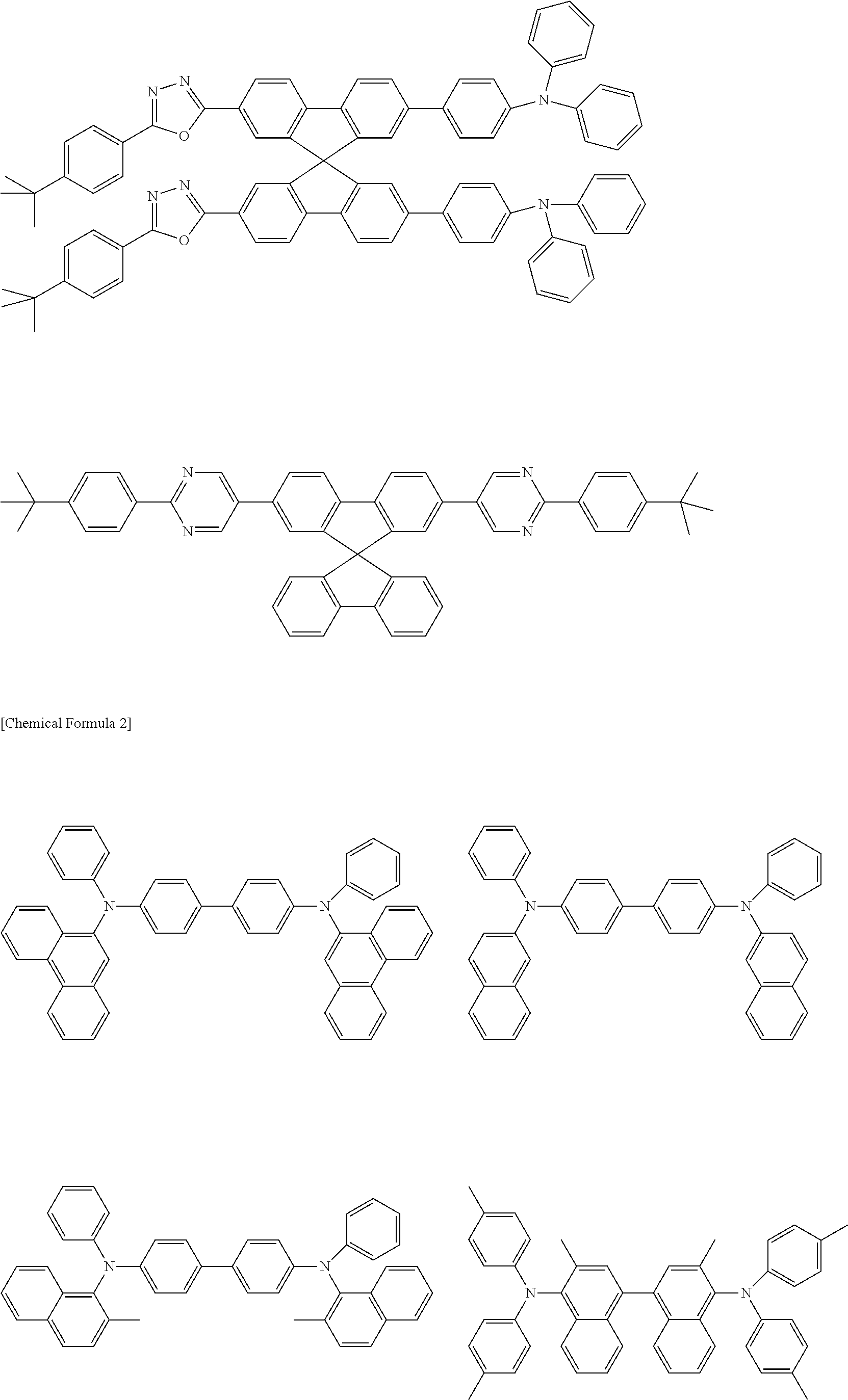
- Examples of preferred compounds which can be used as host material are shown below.
- R and R 1 to R 10 each independently represent a hydrogen atom or a substituent; and n represents an integer of 3 to 5.
- the delayed fluorescent material be a thermally activated delayed fluorescent material that allows reverse intersystem crossing from an excited triplet state to an excited singlet state by absorption of thermal energy.
- the thermally activated delayed fluorescent material relatively easily allows reverse intersystem crossing from an excited triplet state to an excited singlet state by absorbing heat generated by a device and thus allows the excited triplet energy to efficiently contribute to light emission.
- the delayed fluorescent material be an organic compound that has a smaller minimum excited singlet energy than the host material and has a larger minimum excited singlet energy than the luminescent material.
- the delayed fluorescent material has a difference ⁇ E st between the energy level E s1 in the minimum excited singlet state and the energy level E T1 in the minimum excited triplet state at 77 K of 0.3 eV or less, 0.2 eV or less, 0.1 eV or less, and 0.08 eV or less. In some example embodiments, a lower difference ⁇ E st may be preferable. With an energy difference ⁇ E st in the range of approximately 0.3 eV or less, the delayed fluorescent material relatively easily allows reverse intersystem crossing from an excited triplet state to an excited singlet state, allowing the excited triplet energy to efficiently contribute to light emission.
- the luminescent material receives energy from the host material in the excited singlet state and the delayed fluorescent material, and the delayed fluorescent material in the excited singlet state reached from the excited triplet state through reverse intersystem crossing so as to transition to the singlet excited state, and emits fluorescence when returned to the ground state thereafter.
- the luminescent material is not particularly limited as long as it can receive energy from the host material and the delayed fluorescent material so as to emit light, and the emitted light may be fluorescence or delayed fluorescence.
- P ABS of the luminescent material maximum value at the longest wavelength side of absorption spectrum
- a luminescent material having a luminescence peak in a normal near-infrared range when used as dopant be selected as the luminescent material.
- Specific examples thereof include the compounds shown below.
- each of the delayed fluorescent material and the luminescent material may have a N-containing structure with two or three benzene rings bonded to an N atom, wherein two of the benzene rings are optionally bonded to each other to form a fused ring.
- the two benzene rings may be bonded through, for example, a single bond, a carbon atom, an oxygen atom, a sulfur atom, or a nitrogen atom so as to form a fused ring.
- the carbon atom may have one or two substituents, or may form a carbonyl group together with an oxygen atom.
- Specific examples of the fused ring that can be formed include the structures (2) to (6) shown below.
- the N-containing structure described above be a structure selected from the structures (1) to (6) shown below. In other example embodiments, it is more preferable that the N-containing structure be the structure (1) or (2), or the structure (1). And in still example embodiments, it is more preferable that the N-containing structure be the structure (7).
- the benzene ring may further form a fused ring such as a naphthalene ring together with another aromatic ring or heterocycle, in some example embodiments it is preferable that the benzene ring not form a fused ring.
- the structure (1) to (7) may have one or more substituents.
- the examples of the substituents include alkyl groups having 1 to 6 carbon atoms, aryl groups having 6 to 10 carbon atoms and cyano groups.
- each of the delayed fluorescent material and the luminescent material further have a fused ring in addition to the N-containing structure described above, and the fused ring structure of the delayed fluorescent material and the luminescent material each comprise an equivalent set of at least two successive rings, i.e. the fused rings of the delayed fluorescent material and the luminescent material having a common structure of at least two successive rings.
- fused rings of the delayed fluorescent material and the luminescent material having a common structure of at least two successive rings. Examples of such structures include the structures shown below.
- the apparent position of the double bonds in the chemical formulas are not necessarily the same because the double bonds are delocalized in the fused rings.
- the position of the double bonds is different; however, the two successive rings in the formula (A) are equivalent to those in the formula (B).
- the fused ring represented by formula (B) can also be represented by the following formula (B′).
- each of the delayed fluorescent material and the luminescent material further has a common heterocycle (preferably an aromatic heterocycle) or a cyano group, in addition to the N-containing structures described above.
- a common heterocycle preferably an aromatic heterocycle
- a cyano group in addition to the N-containing structures described above.
- heterocycles include the structures shown below. These heterocycles may further form a fused ring together with another benzene ring or heterocycle.
- the content of each organic compound contained in the luminescent layer is not particularly limited, it is preferable that the contents of the delayed fluorescent material and the luminescent material each be smaller than the content of the host material. As a result, a higher luminous efficiency can be achieved.
- the host material content W1 is preferably 15 wt % to 99.9 wt %, 50 wt % to 90 wt %, or 70 wt % to 80 wt %
- the delayed fluorescent material content W2 is preferably 5.0 wt % to 50 wt %, 5.0 wt % to 45 wt %, or 10 wt % to 40 wt %
- the luminescent material content W3 is preferably 0.1 wt % to 5.0 wt %, 0.3 wt % to 4.0 wt
- the luminescent layer may include the host material, the delayed fluorescent material and the luminescent material only, or may include organic compounds in addition to those.
- organic compounds include organic compounds having carrier (electron and/or hole) transport capability.
- hole transport capability and electron transport capability the following hole transport materials and electron transport materials may be referred to, respectively.
- the organic EL element of the present invention be supported by a substrate.
- a substrate Any substrate that is conventionally used for organic EL elements may be used without particular limitation, and, for example, a substrate made of glass, transparent plastic, quartz, or silicon may be used.
- a positive electrode of an organic EL element that includes electrode material made of metal, alloy, electrically conductive compound, or mixture thereof having a large work function (4 eV or more) is preferably used.
- electrode material include metals such as Au, and transparent conductive materials such as, CuI, indium tin oxide (ITO), SnO 2 , and ZnO.
- transparent conductive materials such as, CuI, indium tin oxide (ITO), SnO 2 , and ZnO.
- amorphous material such as IZO (In 2 O 3 —ZnO) from which a transparent conductive film can be made may be used.
- a thin film formed from those electrode materials by a method such as deposition or sputtering may be subjected to photolithography to form a pattern with a desired shape, alternatively in the case of not needing a precise pattern (about 100 ⁇ m or more), the pattern may be formed through a mask with a desired shape when the electrode material is deposited or sputtered.
- a wet deposition method such as printing and coating may also be used.
- the transmittance be controlled to be higher than 10%, and it is preferable that the sheet resistance as positive electrode be several hundred Wsq. or less.
- the film thickness is selected usually from a range of 10 to 1000 nm, preferably from a range of 10 to 200 nm, depending on its material.
- the negative electrode that includes electrode material made of metal (referred to as electron injecting metal), alloy, electrically conductive compound, or mixture thereof having a small work function (4 eV or less) is used.
- electrode material made of metal (referred to as electron injecting metal), alloy, electrically conductive compound, or mixture thereof having a small work function (4 eV or less)
- specific examples of such electrode materials include sodium, sodium-potassium alloy, magnesium, lithium, magnesium/copper mixture, magnesium/silver mixture, magnesium/aluminum mixture, magnesium/indium mixture, aluminum/aluminum oxide (Al 2 O 3 ) mixture, indium, lithium/aluminum mixture, and rare earth metals.
- a mixture of an electron injecting metal and a stable second metal having a larger work function than the electron injecting metal is preferred, including magnesium/silver mixture, magnesium/aluminum mixture, magnesium/indium mixture, aluminum/aluminum oxide (Al 2 O 3 ) mixture, lithium/aluminum mixture, and aluminum.
- the negative electrode can be manufactured by forming a thin film from these electrode materials by a method such as deposition or sputtering. In some example embodiments, it is preferable that the sheet resistance as negative electrode be several hundred ⁇ /sq.
- any one of the positive electrode and the negative electrode of the organic EL element be transparent or translucent for improvement in luminance.
- the transparent conductive materials given as examples in the section of positive electrode may be used to manufacture a transparent or translucent negative electrode, and by applying them, an element with both of the positive electrode and the negative electrode having transparency can be manufactured.
- the injection layer is a layer disposed between the electrode and the organic layer for reduction in driving voltage and improvement in luminance, including a hole injection layer and an electron injection layer, which may be present between the positive electrode and the luminescent layer or the hole transport layer, and between the negative electrode and the luminescent layer or the electron transport layer.
- the injection layer may be disposed on an as needed basis.
- the blocking layer is a layer that can block the diffusion of electric charges (electrons or holes) and/or excitons present in the luminescent layer to the outside of the luminescent layer.
- the electron blocking layer can be disposed between the luminescent layer and the hole transport layer so as to block the electrons from passing through the luminescent layer toward the hole transport layer.
- the hole blocking layer can be disposed between the luminescent layer and the electron transport layer so as to block the holes from passing through the luminescent layer toward the electron transport layer.
- the blocking layer can also be used to block the excitons from diffusing to the outside of the luminescent layer.
- each of the electron blocking layer and the hole blocking layer may double as the exciton blocking layer.
- the electron blocking layer or exciton blocking layer herein means a layer having both functions of the electron blocking layer and the exciton blocking layer in itself.
- the hole blocking layer in a broad sense has the function of an electron transport layer.
- the hole blocking layer has roles for transporting electrons while blocking holes from reaching the electron transport layer, so that the probability of recombination of electrons and holes in the luminescent layer can be improved.
- the electron blocking layer in a broad sense has the function for transporting holes.
- the electron blocking layer has roles for transporting holes while blocking electrons from reaching the hole transport layer, so that the probability of recombination of electrons and holes in the luminescent layer can be improved.
- the exciton blocking layer is a layer for blocking the exciton generated by the recombination of the holes and electrons in the luminescent layer from diffusing into the charge transport layer, of which insertion allows the excitons to be efficiently confined in the luminescent layer to thereby improve the luminous efficiency of an element.
- the exciton blocking layer may be inserted adjacent to the luminescent layer, on any of the positive electrode-side and the negative electrode-side, and insertion on both sides at one time is also possible.
- the layer when having the exciton blocking layer on the positive electrode-side, the layer may be inserted between the hole transport layer and the luminescent layer, adjacent to the luminescent layer; and when inserted on the negative electrode-side, the layer may be inserted between the luminescent layer and the negative electrode, adjacent to the luminescent layer. Also, between the positive electrode and the exciton blocking layer adjacent to the luminescent layer on the positive electrode-side, the hole injection layer, the electron blocking layer, and the like may be included; and between the negative electrode and the exciton blocking layer adjacent to the luminescent layer on the negative electrode-side, the electron injection layer, the electron transport layer, the hole blocking layer, and the like may be included. When a blocking layer is disposed, it is preferable that at least any one of the excited singlet energy and the excited triplet energy of the material for use as blocking layer be higher than the excited singlet energy and the excited triplet energy of the luminescent material.
- the hole transport material has any of hole injection or transport properties and electron barrier properties, and may be any of an organic material and an inorganic material.
- the hole transport material for use include a triazole derivative, an oxadiazole derivative, an imidazole derivative, a carbazole derivative, an indolocarbazole derivative, a polyarylalkan derivative, a pyrazoline derivative and a pyrazolone derivative, a phenylenediamine derivative, an arylamine derivative, an amino-substituted chalcone derivative, an oxazole derivative, a styrylanthracene derivative, a fluorenone derivative, a hydrazone derivative, a stilbene derivative, a silazane derivative, an aniline copolymer, and an electrically conductive polymer/oligomer, a thiophene oligomer in particular; while in some example embodiments, it is preferable to use a porphyrin compound, an aromatic tertiary
- the electron transport layer is made of material having a function for transporting electrons, and can be disposed as a single layer or multi layers.
- the electron transport material (which doubles as hole blocking material in some cases) has only to satisfy the function for transmitting electrons injected from the negative electrode to the luminescent layer.
- the electron transport layer for use include a nitro-substituted fluorene derivative, a diphenylquinone derivative, a thiopyrandioxide derivative, carbodiimide, a fluorenylidene methane derivative, anthraquinodimethane and anthrone derivatives, and an oxadiazole derivative.
- a thiadiazole derivative obtained by substituting the oxygen atom of the oxadiazole ring of the oxadiazole derivative with a sulfur atom, and a quinoxaline derivative having a quinoxaline ring known as electron-withdrawing group can also be used as the electron transport material.
- polymer materials having a polymer chain in which these materials are introduced or having a main chain of these materials can also be used.
- the deposition method of these layers is not particularly limited, and any of a dry process and a wet process can be employed.
- conventionally known organic compounds such as the compounds described in Patent Literature 1 can be used.
- Each of the films may include one organic compound only or two or more organic compounds.
- the organic EL element having the constituents described above emits light when an electric field is applied between the positive electrode and the negative electrode. According to the organic EL element of the present invention, fluorescence emission due to the excited singlet energy is the main luminescence.
- the organic EL element of the present invention can be applied to any of a single element, an element having array structure, and a structure having positive electrode and negative electrode disposed in an X-Y matrix form.
- the organic EL element of the present invention emits light in a near-infrared range, being applicable as, for example, a light source for optical communication, a light source for biometrics, and a light source for sensors, other than the bioinstrumentation devices described above.
- the bioinstrumentation device comprises the organic EL element described above and a photo detector. According to the present device, an organism is exposed to the light in a near-infrared range from the organic EL element as light source for the measurement of the change in the intensity of optical absorption, reflected light, scattered light, and luminescence caused by the biological tissues, so that biological sensing can be performed.
- an organic layer described below was laminated by vacuum deposition.
- ITO indium tin oxide
- an HATCN layer was formed on the ITO, and a TAPC layer was then formed thereon.
- CBP host material
- TPA-DCPP delayed fluorescent material
- TPA-ThQ luminescent material
- the mass ratio of CBP:TPA-DCPP:TPA-ThQ was set at 75:24:1.0.
- a T2T layer was formed and a BPyTP2 layer was formed thereon.
- the total thickness (from HATCN to BpyTP2) of the organic layer was 120 nm. Furthermore, lithium fluoride (LiF) was vacuum deposited to a thickness of 0.8 nm, and aluminum (Al) was then deposited to a thickness of 100 nm to form a negative electrode, so that an organic EL element was obtained.
- LiF lithium fluoride
- Al aluminum
- An organic EL element was obtained in the same manner as in Example 1, except that 4CzIPN-Me was used as the delayed fluorescent material instead of TPA-DCPP.
- ⁇ edge [nm] was defined as the wavelength at the intersection between the tangent line drawn along the trailing gradient on the long wavelength side of the longest wavelength-side peak of each of the obtained absorption spectra and the horizontal axis (wavelength axis), and the calculation was performed based on the formula 2 shown below, using the value of HOMO [eV] obtained by the method described above.
- the tangent line along the trailing gradient was drawn as follows. Moving along the spectral curve from the long wavelength side to the maximal value of an absorption peak, tangent lines may be drawn on the respective points on the spectral curve. The slope of the tangent lines increases as the curve rises (in other words, as the vertical axis increases). A tangent line drawn at the maximal value of the slope was defined as the tangent line along the trailing gradient on the long wavelength side of the absorption spectrum.
- a host material and a delayed fluorescent material were deposited such that the mass ratio therebetween was the same as the ratio in Examples or Comparative Examples, and the emission spectrum was measured by a fluorescence spectrophotometer FLUOROMAX (manufactured by Horiba, Ltd.).
- FLUOROMAX fluorescence spectrophotometer
- P Em was defined as the maximal value at the longest wavelength side of the spectrum obtained in the present measurement.
- the slit width at the upstream or the downstream was 10 nm or less, and the film thickness was 30 nm or more and 200 nm or less.
- the organic EL element of Example 1 has a maximum luminescence in a near-infrared range of 700 nm or more (near a wavelength of 760 nm), without the presence of a maximum luminescence in the visible light range.
- each organic EL element in Comparative Examples 1 and 2 has a maximum luminescence in a near-infrared range of 700 nm or more (near a wavelength of 760 nm), and with the presence of a maximum luminescence derived from the delayed fluorescent material in the visible light range.
- the organic EL element of Example 1 requires a smaller voltage to obtain the same level of luminance in comparison with the organic EL elements in Comparative Examples 1 and 2, which means that the organic EL element has excellent electric properties. Additionally, the organic EL element has a very small lowering ratio of chronological output to the initial output, which clearly means that the organic EL element has a long device life.
Abstract
Description
- [Patent Literature 1] JP5669163 B1
- [Non Patent Literature 1] G. Qian et al. J. Phys. Chem. C 2009, 113, 1589-1595
- [Non Patent Literature 2] X. Du et al. Chem. Mater. 2012, 24, 2178-2185
- [Non Patent Literature 3] G. Qian et al. Adv. Mater. 2009, 21, 111-116
- [Non Patent Literature 4] U. Mayerhoeffer et al. Chem. Eur. J. 2013, 19, 218-232
- [Non Patent Literature 5] M. T. Sharbatia et al. Optik, 2013, 124, 52-54
- [Non Patent Literature 6] X. Zhang et al. J. Org. Chem. 2013, 78, 9153-9160
ΔHOMO+ΔLUMO≤0.6 eV (1);
|ΔHOMO|≤0.4 eV (2);
|ΔLUMO|≤0.4 eV (3)
-
- wherein “ΔHOMO” represents a value of a highest occupied molecular orbital (HOMO) energy level of the luminescent material minus a HOMO energy level of the delayed fluorescent material, and “ΔLUMO” represents a value of a lowest unoccupied molecular orbital (LUMO) energy level of the delayed fluorescent material minus a LUMO energy level of the luminescent material; and
|P Abs −P Em|≤30 nm (4) - wherein PAbs represents a maximal value at the longest wavelength side of an absorption spectrum of the luminescent material, and PEm represents a maximal value at the longest wavelength side of an emission spectrum of the delayed fluorescent material.
- wherein “ΔHOMO” represents a value of a highest occupied molecular orbital (HOMO) energy level of the luminescent material minus a HOMO energy level of the delayed fluorescent material, and “ΔLUMO” represents a value of a lowest unoccupied molecular orbital (LUMO) energy level of the delayed fluorescent material minus a LUMO energy level of the luminescent material; and
ΔHOMO+ΔLUMO≤0.6 eV (1);
|ΔHOMO|≤0.4 eV (2);
|ΔLUMO|≤0.4 eV (3)
|P Abs −P Em|≤30 nm (4)


- S. Wang et al. Angew. Chem. Int. ed. 2015, 54, 1-6
- J. Lee et al. J. Mater. Chem. C, 2015, 3, 2175-2181
- Q. Zhang et al. J. Am. Chem. Soc. 2014, 136, 18070-18081
- H. Uoyama et al. Nature 2012, 492, 234-238


- G. Qian et al. J. Phys. Chem. C 2009, 113, 1589-1595
- X. Du et al. Chem. Mater. 2012, 24, 2178-2185
- G. Qian et al. Adv. Mater. 2009, 21, 111-116
- U. Mayerhoeffer et al. Chem. Eur. J. 2013, 19, 218-232
- M. T. Sharbatia et al. Optik, 2013, 124, 52-54
- X. Zhang et al. J. Org. Chem. 2013, 78, 9153-9160


| TABLE 1 | |||
| Luminescent | |||
| material | Delayed fluorescent material | ||
| TPA-ThQ | TPA-DCPP | 4CzIPN—Me | 4CzTPN—Ph | ||
| PAbs | 640 | nm | — | — | — |
| PEm | — | 650 | nm | 550 | |
600 | nm |
| ΔP | — | 10 | nm | 90 | |
40 | nm |
| LUMO | 4.1 | eV | 4.0 | eV | 3.5 | eV | 4.4 | eV |
| ΔLUMO | — | 0.1 | eV | 0.6 | eV | −0.3 | eV |
| HOMO | 5.7 | eV | 5.9 | eV | 5.9 | eV | 6.3 | eV |
| ΔHOMO | — | 0.2 | eV | 0.2 | eV | 0.6 | eV |
Claims (20)
ΔHOMO+ΔLUMO≤0.6 eV (1);
|ΔHOMO|≤0.4 eV (2);
|ΔLUMO|≤0.4 eV (3); and
|P Abs −P Em|≤30 nm (4),
ΔHOMO+ΔLUMO≤0.6 eV (1);
|ΔHOMO|≤0.4 eV (2);
|ΔLUMO|≤0.4 eV (3); and
|P Abs −P Em|≤30 nm (4),
Applications Claiming Priority (2)
| Application Number | Priority Date | Filing Date | Title |
|---|---|---|---|
| JP2016233234A JP6890784B2 (en) | 2016-11-30 | 2016-11-30 | Organic electroluminescence device and biometric device |
| JP2016-233234 | 2016-11-30 |
Publications (2)
| Publication Number | Publication Date |
|---|---|
| US20180149595A1 US20180149595A1 (en) | 2018-05-31 |
| US10228328B2 true US10228328B2 (en) | 2019-03-12 |
Family
ID=62190077
Family Applications (1)
| Application Number | Title | Priority Date | Filing Date |
|---|---|---|---|
| US15/823,599 Active US10228328B2 (en) | 2016-11-30 | 2017-11-28 | Organic electro-luminescent element and bioinstrumentation device |
Country Status (2)
| Country | Link |
|---|---|
| US (1) | US10228328B2 (en) |
| JP (1) | JP6890784B2 (en) |
Cited By (1)
| Publication number | Priority date | Publication date | Assignee | Title |
|---|---|---|---|---|
| US20180151810A1 (en) * | 2016-11-30 | 2018-05-31 | Kyushu University, National University Corporation | Organic electro-luminescent element and bioinstrumentation device |
Families Citing this family (8)
| Publication number | Priority date | Publication date | Assignee | Title |
|---|---|---|---|---|
| JP7044108B2 (en) * | 2017-05-08 | 2022-03-30 | コニカミノルタ株式会社 | Organic electroluminescence elements, display devices, lighting devices |
| KR102585841B1 (en) | 2018-10-10 | 2023-10-05 | 엘지디스플레이 주식회사 | Organic light emitting diode and organic light emitting device having the diode |
| CN109449303B (en) * | 2018-11-06 | 2021-03-02 | 固安翌光科技有限公司 | OLED device |
| CN110044973A (en) * | 2019-05-05 | 2019-07-23 | 吉林大学 | Plane formula room temperature ammonia gas sensor and preparation method thereof based on the organic sensitive thin film of TPA-DCPP |
| WO2020240333A1 (en) * | 2019-05-31 | 2020-12-03 | 株式会社半導体エネルギー研究所 | Light emitting device, light emitting apparatus, light emitting module, electronic device, and lighting device |
| JPWO2021111227A1 (en) * | 2019-12-02 | 2021-06-10 | ||
| US20230255045A1 (en) * | 2021-01-22 | 2023-08-10 | Boe Technology Group Co., Ltd. | Organic Light Emitting Device and Display Apparatus |
| WO2023184103A1 (en) * | 2022-03-28 | 2023-10-05 | 京东方科技集团股份有限公司 | Light-emitting device and preparation method therefor, and display apparatus |
Citations (6)
| Publication number | Priority date | Publication date | Assignee | Title |
|---|---|---|---|---|
| JP5669163B1 (en) | 2013-08-14 | 2015-02-12 | 国立大学法人九州大学 | Organic electroluminescence device |
| US20160372688A1 (en) * | 2015-06-17 | 2016-12-22 | Semiconductor Energy Laboratory Co., Ltd. | Iridium complex, light-emitting element, display device, electronic device, and lighting device |
| US20170123268A1 (en) * | 2015-10-30 | 2017-05-04 | Semiconductor Energy Laboratory Co., Ltd. | Display device, electronic device, and method for manufacturing display device and electronic device |
| US20170324055A1 (en) * | 2016-05-06 | 2017-11-09 | Semiconductor Energy Laboratory Co., Ltd. | Light-emitting element, display device, electronic device, and lighting device |
| US20180151810A1 (en) | 2016-11-30 | 2018-05-31 | Kyushu University, National University Corporation | Organic electro-luminescent element and bioinstrumentation device |
| JP2018093175A (en) | 2016-11-30 | 2018-06-14 | 国立大学法人九州大学 | Organic electroluminescent device and bioinstrumentation device |
Family Cites Families (12)
| Publication number | Priority date | Publication date | Assignee | Title |
|---|---|---|---|---|
| JP2012221082A (en) * | 2011-04-06 | 2012-11-12 | Seiko Epson Corp | Sensing device and electronic apparatus |
| JP5682429B2 (en) * | 2011-04-12 | 2015-03-11 | セイコーエプソン株式会社 | Thiadiazole compounds, compounds for light emitting devices, light emitting devices, light emitting devices, authentication devices, and electronic devices |
| JP5790279B2 (en) * | 2011-08-09 | 2015-10-07 | セイコーエプソン株式会社 | LIGHT EMITTING ELEMENT, LIGHT EMITTING DEVICE, AND ELECTRONIC DEVICE |
| JP6424456B2 (en) * | 2013-07-17 | 2018-11-21 | セイコーエプソン株式会社 | Light emitting device, method of manufacturing light emitting device, light emitting and receiving device, electronic device |
| JP6269112B2 (en) * | 2014-01-31 | 2018-01-31 | セイコーエプソン株式会社 | Image acquisition device, image acquisition device manufacturing method, and electronic apparatus |
| JP6459228B2 (en) * | 2014-06-02 | 2019-01-30 | セイコーエプソン株式会社 | LIGHT EMITTING DEVICE, ELECTRONIC DEVICE, AND INSPECTION METHOD |
| CN109378396B (en) * | 2014-07-31 | 2021-01-26 | 柯尼卡美能达株式会社 | Organic electroluminescent element, display device, lighting device, pi-conjugated compound, and light-emitting thin film |
| JP2016119355A (en) * | 2014-12-19 | 2016-06-30 | コニカミノルタ株式会社 | Organic electroluminescent element |
| JPWO2016181844A1 (en) * | 2015-05-08 | 2018-02-22 | コニカミノルタ株式会社 | π-conjugated compound, delayed phosphor, light-emitting thin film, organic electroluminescence element, display device, and illumination device |
| JP7081924B2 (en) * | 2015-05-08 | 2022-06-07 | メルク パテント ゲゼルシャフト ミット ベシュレンクテル ハフツング | Luminescent material, luminescent thin film, organic electroluminescence element, display device and lighting device |
| CN104830320B (en) * | 2015-05-24 | 2017-03-22 | 吉林大学 | Phenanthreneopyrazine derivative luminescent material and application thereof in electroluminescent device |
| WO2018008721A1 (en) * | 2016-07-08 | 2018-01-11 | コニカミノルタ株式会社 | Organic electroluminescent element, display device, and illumination device |
-
2016
- 2016-11-30 JP JP2016233234A patent/JP6890784B2/en active Active
-
2017
- 2017-11-28 US US15/823,599 patent/US10228328B2/en active Active
Patent Citations (7)
| Publication number | Priority date | Publication date | Assignee | Title |
|---|---|---|---|---|
| JP5669163B1 (en) | 2013-08-14 | 2015-02-12 | 国立大学法人九州大学 | Organic electroluminescence device |
| US20160190478A1 (en) | 2013-08-14 | 2016-06-30 | Kyushu University, National University Corporation | Organic electroluminescent device |
| US20160372688A1 (en) * | 2015-06-17 | 2016-12-22 | Semiconductor Energy Laboratory Co., Ltd. | Iridium complex, light-emitting element, display device, electronic device, and lighting device |
| US20170123268A1 (en) * | 2015-10-30 | 2017-05-04 | Semiconductor Energy Laboratory Co., Ltd. | Display device, electronic device, and method for manufacturing display device and electronic device |
| US20170324055A1 (en) * | 2016-05-06 | 2017-11-09 | Semiconductor Energy Laboratory Co., Ltd. | Light-emitting element, display device, electronic device, and lighting device |
| US20180151810A1 (en) | 2016-11-30 | 2018-05-31 | Kyushu University, National University Corporation | Organic electro-luminescent element and bioinstrumentation device |
| JP2018093175A (en) | 2016-11-30 | 2018-06-14 | 国立大学法人九州大学 | Organic electroluminescent device and bioinstrumentation device |
Non-Patent Citations (11)
Cited By (2)
| Publication number | Priority date | Publication date | Assignee | Title |
|---|---|---|---|---|
| US20180151810A1 (en) * | 2016-11-30 | 2018-05-31 | Kyushu University, National University Corporation | Organic electro-luminescent element and bioinstrumentation device |
| US11444248B2 (en) * | 2016-11-30 | 2022-09-13 | Kyushu University, National University Corporation | Organic electro-luminescent element and bioinstrumentation device |
Also Published As
| Publication number | Publication date |
|---|---|
| JP2018092993A (en) | 2018-06-14 |
| JP6890784B2 (en) | 2021-06-18 |
| US20180149595A1 (en) | 2018-05-31 |
Similar Documents
| Publication | Publication Date | Title |
|---|---|---|
| US10228328B2 (en) | Organic electro-luminescent element and bioinstrumentation device | |
| US10600983B2 (en) | Organic electroluminescent device comprising delayed fluorescent materials | |
| US10995265B2 (en) | Thin film and organic light-emitting device including the same | |
| US9257663B2 (en) | Organic electroluminescent element and display device | |
| EP2247163B1 (en) | Organic luminescent device and a production method for the same | |
| EP3171421B1 (en) | Organic light-emitting element | |
| US8227094B2 (en) | Organic electroluminescent device | |
| Yang et al. | Ultraviolet-violet electroluminescence from highly fluorescent purines | |
| US20100176380A1 (en) | Organic photoelectric device and material used therein | |
| US11444248B2 (en) | Organic electro-luminescent element and bioinstrumentation device | |
| US20060099451A1 (en) | Organic electroluminescent device | |
| US11825737B2 (en) | Organometallic compound, organic light-emitting device including the organometallic compound, and diagnostic composition including the organometallic compound | |
| TW201245405A (en) | Organic electronic device for lighting | |
| US20090015150A1 (en) | Organic light emitting device and method for manufacturing the same | |
| JP2016051693A (en) | Organic semiconductor element manufacturing method and organic semiconductor element | |
| JP6869509B2 (en) | Organic electroluminescence device and biometric device | |
| US8217392B2 (en) | Organic electroluminescence element | |
| US8212472B2 (en) | Organic electric field light-emitting element | |
| JP7337369B2 (en) | Organic light emitting device, laminate and light emitting method | |
| KR102339891B1 (en) | organic electroluminescent device |
Legal Events
| Date | Code | Title | Description |
|---|---|---|---|
| AS | Assignment |
Owner name: HAMAMATSU PHOTONICS K.K., JAPAN Free format text: ASSIGNMENT OF ASSIGNORS INTEREST;ASSIGNORS:ADACHI, CHIHAYA;NAKANOTANI, HAJIME;YAMANAKA, TAKAHIKO;AND OTHERS;SIGNING DATES FROM 20171114 TO 20171116;REEL/FRAME:044231/0054 Owner name: KYUSHU UNIVERSITY, NATIONAL UNIVERSITY CORPORATION Free format text: ASSIGNMENT OF ASSIGNORS INTEREST;ASSIGNORS:ADACHI, CHIHAYA;NAKANOTANI, HAJIME;YAMANAKA, TAKAHIKO;AND OTHERS;SIGNING DATES FROM 20171114 TO 20171116;REEL/FRAME:044231/0054 |
|
| FEPP | Fee payment procedure |
Free format text: ENTITY STATUS SET TO UNDISCOUNTED (ORIGINAL EVENT CODE: BIG.); ENTITY STATUS OF PATENT OWNER: LARGE ENTITY |
|
| STCF | Information on status: patent grant |
Free format text: PATENTED CASE |
|
| CC | Certificate of correction | ||
| MAFP | Maintenance fee payment |
Free format text: PAYMENT OF MAINTENANCE FEE, 4TH YEAR, LARGE ENTITY (ORIGINAL EVENT CODE: M1551); ENTITY STATUS OF PATENT OWNER: LARGE ENTITY Year of fee payment: 4 |