US10216333B2 - Phase error compensation in single correlator systems - Google Patents
Phase error compensation in single correlator systems Download PDFInfo
- Publication number
- US10216333B2 US10216333B2 US15/639,420 US201715639420A US10216333B2 US 10216333 B2 US10216333 B2 US 10216333B2 US 201715639420 A US201715639420 A US 201715639420A US 10216333 B2 US10216333 B2 US 10216333B2
- Authority
- US
- United States
- Prior art keywords
- digitizer
- touch screen
- stylus
- screen display
- signal
- Prior art date
- Legal status (The legal status is an assumption and is not a legal conclusion. Google has not performed a legal analysis and makes no representation as to the accuracy of the status listed.)
- Active
Links
Images


Classifications
-
- G—PHYSICS
- G06—COMPUTING OR CALCULATING; COUNTING
- G06F—ELECTRIC DIGITAL DATA PROCESSING
- G06F3/00—Input arrangements for transferring data to be processed into a form capable of being handled by the computer; Output arrangements for transferring data from processing unit to output unit, e.g. interface arrangements
- G06F3/01—Input arrangements or combined input and output arrangements for interaction between user and computer
- G06F3/03—Arrangements for converting the position or the displacement of a member into a coded form
- G06F3/041—Digitisers, e.g. for touch screens or touch pads, characterised by the transducing means
- G06F3/0416—Control or interface arrangements specially adapted for digitisers
- G06F3/0418—Control or interface arrangements specially adapted for digitisers for error correction or compensation, e.g. based on parallax, calibration or alignment
-
- G—PHYSICS
- G06—COMPUTING OR CALCULATING; COUNTING
- G06F—ELECTRIC DIGITAL DATA PROCESSING
- G06F3/00—Input arrangements for transferring data to be processed into a form capable of being handled by the computer; Output arrangements for transferring data from processing unit to output unit, e.g. interface arrangements
- G06F3/01—Input arrangements or combined input and output arrangements for interaction between user and computer
- G06F3/03—Arrangements for converting the position or the displacement of a member into a coded form
- G06F3/033—Pointing devices displaced or positioned by the user, e.g. mice, trackballs, pens or joysticks; Accessories therefor
- G06F3/0354—Pointing devices displaced or positioned by the user, e.g. mice, trackballs, pens or joysticks; Accessories therefor with detection of two-dimensional [2D] relative movements between the device, or an operating part thereof, and a plane or surface, e.g. 2D mice, trackballs, pens or pucks
- G06F3/03545—Pens or stylus
-
- G—PHYSICS
- G06—COMPUTING OR CALCULATING; COUNTING
- G06F—ELECTRIC DIGITAL DATA PROCESSING
- G06F3/00—Input arrangements for transferring data to be processed into a form capable of being handled by the computer; Output arrangements for transferring data from processing unit to output unit, e.g. interface arrangements
- G06F3/01—Input arrangements or combined input and output arrangements for interaction between user and computer
- G06F3/03—Arrangements for converting the position or the displacement of a member into a coded form
- G06F3/041—Digitisers, e.g. for touch screens or touch pads, characterised by the transducing means
- G06F3/0412—Digitisers structurally integrated in a display
-
- G—PHYSICS
- G06—COMPUTING OR CALCULATING; COUNTING
- G06F—ELECTRIC DIGITAL DATA PROCESSING
- G06F3/00—Input arrangements for transferring data to be processed into a form capable of being handled by the computer; Output arrangements for transferring data from processing unit to output unit, e.g. interface arrangements
- G06F3/01—Input arrangements or combined input and output arrangements for interaction between user and computer
- G06F3/03—Arrangements for converting the position or the displacement of a member into a coded form
- G06F3/041—Digitisers, e.g. for touch screens or touch pads, characterised by the transducing means
- G06F3/044—Digitisers, e.g. for touch screens or touch pads, characterised by the transducing means by capacitive means
- G06F3/0442—Digitisers, e.g. for touch screens or touch pads, characterised by the transducing means by capacitive means using active external devices, e.g. active pens, for transmitting changes in electrical potential to be received by the digitiser
Definitions
- Touch screen displays are commonplace in today's commercial electronic devices. Such displays are finding widespread use in many new products, such as cellular phones, personal digital assistants (PDAs), camcorders, and laptop personal computers (PCs). Touch screen displays can be configured with either a finger touch input and/or a stylus (or “pen”) touch input. Over the years, a number of touch detection technologies have been developed that allow the touch screen display to accurately identify the location of the touch on the display screen.
- capacitive touch panels that identify the point of the touch using sensors that detect changes in electrical current generated by contact with a finger and/or stylus that change the electrostatic capacity (e.g., load).
- electrostatic capacity e.g., load
- capacitive touch panels There are two types of capacitive touch panels: surface capacitive touch panels and projected capacitive touch panels.
- surface capacitive touch panels electric voltage is applied to electrodes positioned in the four corners of the glass substrate, generating a uniform low-voltage electrical field across the entire touch screen display screen. The coordinates of the position at which the finger touches the screen are identified by measuring the resulting changes in electrostatic capacity at the four corners of the panel.
- a layer of transparent electrodes is positioned with the electrodes in a specific pattern and the surface is covered with an insulating glass or plastic cover.
- the electrostatic capacity among multiple electrodes changes simultaneously, and the position where contact occurs can be identified by measuring the ratios between the electrical currents.
- the touch screen displays are unable to leverage the touch of a stylus to accurately identify the stylus touch.
- the touch screen displays may also separately use a “digitizer” to enable communication between the touch screen display and the stylus and the user touch.
- the digitizer is a component used to convert analog signals into digital signals.
- the digitizer may measure self-capacitance to detect and convert user actions (e.g., touch, swipe) into a digital signal that could processed by the electronic device associated with the touch screen display (e.g., tablet, laptop, mobile phone).
- touch screen displays produced today that utilize capacitive touch panels, however, rely on the touch layer to be sandwiched between a display panel (e.g., the panel producing the images for display) and a cover layer (e.g., glass or plastic layer), adding to the overall width of the screen.
- a display panel e.g., the panel producing the images for display
- a cover layer e.g., glass or plastic layer
- display manufacturers have developed “in-cell” touch system that generally refers to the implementation of touch sensors that are physically inside the cell of a display panel. While this removes the need for the touch layer to be a separate layer from the display panel, such integration raise other challenges, including challenges with respect to accurately detecting stylus touch.
- aspects of the present disclosure provide techniques to compensate for the above-identified problem between a digitizer of the touch screen display system and a stylus (or pen).
- a digitizer of the touch screen display system and a stylus (or pen).
- the system may be sensitive to the relative phase between the stylus signal and the correlation signal at the digitizer.
- the delays may be compensated by estimating the stylus-digitizer phase error on the digitizer side and adjusting for the delay accordingly.
- the digitizer may utilize a quadratic receiver to perform an in-phase and quadratic detection in time domain in order to estimate the phase error. Based on the in-phase and quadratic detection, the digitizer may adapt the subsequent stylus sampling windows to compensate for the detected phase error.
- the stylus may transmit a first signal and a second signal that is 90 degrees delayed during a predetermined time slot.
- the quadratic receiver at the digitizer may correlate the received signals to identify the delay and to adapt the stylus sampling windows on the digitizer side in order to compensate for the phase delay.
- the digitizer may also identify the phase delay based on the quadratic receiver and transmit a command, through an uplink signal, to the stylus instructing the stylus to shift the phase at the stylus.
- a method for time synchronizing an in-cell touch screen display with a stylus may include receiving, at a digitizer of the in-cell touch screen display, a downlink signal from the stylus associated with the touch screen display. The method may further include determining, at the digitizer, a timing misalignment between the in-cell touch screen display and the stylus by measuring self-capacitance of a sensel electrode on the in-cell touch screen display based on the downlink signal. In some examples, the method may further include adjusting, at the digitizer, a sampling window to compensate for the timing misalignment.
- an apparatus for time synchronizing an in-cell touch screen display with a stylus may include a processor and a memory coupled to the processor.
- the memory may include instructions executable by the processor to receiving, at a digitizer of the in-cell touch screen display, a downlink signal from the stylus associated with the touch screen display.
- the memory may include instructions executable by the processor to determine, at the digitizer, a timing misalignment between the in-cell touch screen display and the stylus by measuring self-capacitance of a sensel electrode on the in-cell touch screen display based on the downlink signal.
- the instructions may further be executable by the processor to adjust, at the digitizer, a sampling window to compensate for the timing misalignment.
- a computer readable medium for time synchronizing an in-cell touch screen display with a stylus.
- the computer readable medium may include code for receiving, at a digitizer of the in-cell touch screen display, a downlink signal from the stylus associated with the touch screen display.
- the computer readable medium may further include code for determining, at the digitizer, a timing misalignment between the in-cell touch screen display and the stylus by measuring self-capacitance of a sensel electrode on the in-cell touch screen display based on the downlink signal.
- the computer readable medium may further include code for adjusting, at the digitizer, a sampling window to compensate for the timing misalignment.
- FIG. 1 is a schematic diagram of an example of an in-cell touch screen display system that processes signal delays between an in-cell digitizer of the touch screen display system and a stylus in which features of the present disclosure may operate.
- FIG. 2 is a call flow between in-cell digitizer and a stylus implementing one technique of calibrating for timing uncertainty in the transmissions in accordance with various aspects of the present disclosure.
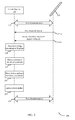
- FIG. 3 is a flowchart of a method for time synchronizing an in-cell touch screen display with a stylus implemented by an in-cell digitizer in accordance with aspects of the present disclosure.
- FIG. 4 is a diagram illustrating an example of a hardware implementation for a touch screen display in accordance with various aspects of the present disclosure.
- an “out-cell” digitizer may utilize a sensor matrix consisting of electrically-conducting rows and columns placed in front of the display panel (or layer). While the in-cell integration allows the manufacturers to develop thinner touch screen display systems, however, the integration also raises additional challenges, especially with respect to the use of a stylus (or pen) on a touch screen displays.
- in-cell touch systems may be limited to a single correlator.
- each electrode e.g., each row and column of electrodes across the touch screen display
- the in-cell touch systems are limited to a single correlator due to silicon area constraints. This is because introducing multiple correlators per channel into an in-cell touch system may require additional hardware that may not be feasible in limited areas.
- the limited single correlator requires the stylus to maintain only a small margin of phase error in order for the stylus and the touch screen display to remain synchronized.
- the digitizer and the stylus may also include variable delays that may be a function of integrated circuit process, voltage, and/or temperature. Failure to correct such delays may result in the stylus and the digitizer falling out of phase from one another and thus be desynchronized.
- the present disclosure provides techniques to compensate for the above-identified signal processing delays between a digitizer of the touch screen display system and a stylus (or pen).
- the digitizer may be an in-cell digitizer or an out-cell digitizer associated with a touch screen display.
- the delays may be compensated by estimating the stylus-digitizer phase error on the digitizer side and adjusting for the delay accordingly.
- the digitizer may utilize a pseudo-quadratic receiver to perform an in-phase and quadratic detection in the time domain in order to estimate the phase error. Based on the in-phase and quadratic detection, the digitizer may adapt its subsequent stylus sampling windows to compensate for the detected phase error.
- the stylus may transmit a first signal and a second signal that is 90 degrees delayed relative to the first signal during a predetermined time slot.
- the quadratic receiver at the digitizer may correlate the received signals to identify the delay and to adapt its stylus sampling windows in order to compensate for the phase delay.
- the present disclosure may enable identifying and compensating for phase delay between the digitizer and the stylus using the existing capacitance circuitry, and therefore without adding any additional cost.
- FIGS. 1-4 Various features are now described in more detail with reference to the FIGS. 1-4 .
- numerous specific details are set forth in order to provide a thorough understanding of one or more aspects. It may be evident, however, that such feature(s) may be practiced without these specific details.
- the term “component” as used herein may be one of the parts that make up a system, may be hardware, firmware, and/or software stored on a computer-readable medium, and may be divided into other components.
- finger touch used throughout this document may generally refer to any physical user contact (e.g., finger, palm, hand) on the touch screen display or a touch sensitive surface of an electronic device using capacitive sensors or the like.
- virtual touch inputs relative to projected displays, electronic whiteboards, or other surfaces are treated in the same manner as actual touch inputs on a touch-sensitive surface of the touch screen display.
- Such virtual touch inputs may be detected using techniques such as, but not limited to, using cameras or other imaging technologies to track user finger movement relative to a projected image, physical object, or text.
- stylus and “pen” may be used interchangeably herein.
- the terms “stylus input” or “pen input” may refer to interaction involving physical contact or near contact (or hover) of the sensor stylus or pen with a touch sensitive surface or digitizer component of the touch screen display or the electronic device.
- a schematic diagram 100 includes an example of an electronic device 105 (e.g., tablet, laptop, mobile phone) that may implement features of the present disclosure described herein with respect to processing signal delays between an digitizer 130 of a touch screen display 110 and a stylus 115 .
- an electronic device 105 e.g., tablet, laptop, mobile phone
- the digitizer 130 may be described with reference to “in-cell digitizer,” it should be appreciated by those of ordinary skill in the art that features of the present disclosure may also be implemented on “out-cell” touch screen displays and digitizers.
- the stylus 115 may be an “active stylus” (or “active pen”) that includes electronic components (e.g., battery, processor) and allows users to write directly onto the surface of the touch screen display 110 .
- active stylus or “active pen” that includes electronic components (e.g., battery, processor) and allows users to write directly onto the surface of the touch screen display 110 .
- the active stylus 115 may provide enhanced functionality to the user, including, but not limited to, controlling touch sensitivity, input buttons, etc.
- the active stylus 115 may also contain electrodes in the tip 125 of the active stylus 115 .
- each of the two paired devices may be synchronized with respect to timing such that when a first device (e.g., stylus 115 ) transmits a signal, the second device (e.g., touch screen display 110 ) may be activing listening for the transmitted signal during one or more predetermined time slots.
- the in-cell digitizer 130 incorporated into the touch screen display 110 may act as a timing master and the stylus 115 may synchronize to it by using beacon signals. Once synchronization is established, communication between the touch screen display 110 and the stylus 115 may be ensue.
- the in-cell touch screen display 110 may also be configured to detect and process user input from a finger touch 120 .
- a finger touch 120 As noted above, current technological advances have allowed display manufacturers to forego a dedicated touch layer by etching the electrodes of the touch sensors, including the digitizers, directly into the layer of the display panel (e.g., LCD) of the touch screen display 110 . Such integration allows for thinner and less bulkier display screens. Consequently, as illustrated in FIG. 1 , the touch screen display 110 may incorporate both the touch sensors (e.g., capacitive touch sensors) and the digitizer 130 as part of the same layer.
- the touch screen display 110 may incorporate both the touch sensors (e.g., capacitive touch sensors) and the digitizer 130 as part of the same layer.
- the terms “digitizer” and “in-cell digitizer” may be used interchangeably to refer to the digitizer that is etched into the display panel of the touch screen display 110 .
- the digitizer 130 may also be capable of measuring self-capacitance on the touch screen display 110 . Measurement of self-capacitance may provide detectability of a finger or stylus touch.
- the touch screen display 110 may apply a voltage on the plurality of sensel electrodes across the display screen in order to measure the current at each sensel electrode.
- the digitizer 130 may report the position of the finger touch to the electronic device 105 .
- the digitizer 130 may measure capacitance to the electrode tip 125 of the stylus 115 by applying a voltage on the electrode tip 125 and measuring the current into the plurality of sensel electrodes, as opposed to measuring capacitances to ground as in the case for finger touch.
- the integration allows the manufacturers to develop a thinner touch screen display 110 , the integration also limits the display systems to only a single correlator due to silicon area constraints.
- utilization of an in-cell digitizer for detection of stylus touch may limit the display screen to only a single correlator.
- the stylus 115 may be required to maintain an extremely small phase error in order to maintain time synchronization between the touch screen display 110 and the stylus 115 .
- the touch screen display 110 and stylus 115 initialize such that the paired devices are time synchronized. Absent time synchronization, the touch screen display 110 and stylus 115 would be unable to communicate effectively, and thus adversely impact user interaction with the touch screen display 110 and stylus 115 (e.g., delayed stylus touch detection, false detections).
- the in-cell digitizer would be required to synchronize the touch screen display 110 and the stylus 115 to within an amount of time that is smaller compared to the period of the measurement signal.
- the touch screen display 110 and stylus 115 would need to maintain less than 2.5 microseconds of timing uncertainty (or “timing misalignment”), which may correspond to a ninety degree phase shift (e.g., if the in-cell digitizer is correlating for sine waveform, then it may actually be receiving a cosine waveform—resulting in a 2.5 microseconds of timing inaccuracy).
- timing misalignment e.g., if the in-cell digitizer is correlating for sine waveform, then it may actually be receiving a cosine waveform—resulting in a 2.5 microseconds of timing inaccuracy.
- a timing offset between the touch screen display 110 and stylus 115 of greater than 2.5 microseconds would result in a complete loss of signal because a correlation reference signal and the received current from the stylus would be out of phase.
- the correlation reference signal may be generated by the digitizer based in part on the internal clock source of the digitizer.
- the hardware architecture of the in-cell digitizers may generate a signal (or waveform) for transmission during a specified time slot at a high level of accuracy, the same is not true once the waveform is sent through the level shifter and a power driver that generate the actual signal that is ultimately applied to the electrodes with a higher voltage and higher current drive.
- components such as level shifter and power driver may introduce a variable delay to the signal that may be based on factors such as temperature, circuit processes, etc.
- the level shifter and the power driver in the stylus 115 may also add delay in signals generated from the stylus 115 that require timing adjustment by either the stylus 115 or the in-cell digitizer aiding the stylus 115 in correcting the phase error.
- the present disclosure time synchronizes the stylus 115 to the in-cell digitizer 130 within the timing requirements of a single correlator by estimating the stylus-digitizer phase error on the digitizer side and adjusting for the delay accordingly.
- the in-cell digitizer 130 may utilize a quadratic receiver to perform an in-phase and quadratic detection in the time domain in order to estimate the phase error. Based on the in-phase and quadratic detection, the digitizer 130 may adapt its subsequent stylus sampling windows to compensate for the detected phase error.
- the stylus 115 may transmit a first signal and a second signal that is 90 degrees delayed relative to the first signal during a predetermined time slot.
- the pseudo quadratic receiver at the digitizer may correlate the received signals to identify the delay and to adapt its stylus sampling windows in order to compensate for the phase delay.
- the digitizer may remain in phase while the stylus 115 may adjust its phase based on commands and signals received on the uplink from the digitizer 130 .
- a call flow diagram 200 illustrates techniques of time synchronizing the in-cell digitizer 130 and the stylus 115 .
- the in-cell digitizer 130 may be an example of the digitizer 130 described as part of the touch screen display 110 in reference to FIG. 1 .
- the stylus 115 may also be an example of the stylus 115 described with reference to FIG. 1 .
- the in-cell digitizer 130 acting as a master, may initialize time synchronization between the in-cell digitizer 130 and the stylus 115 whereby the stylus 115 may synchronize with the in-cell digitizer 130 (and by extension the touch screen display 110 ) using beacon signals to pair the two devices.
- the stylus 115 may transmit a first downlink signal to the in-cell digitizer 130 by applying a voltage on its electrodes at the tip 125 of the stylus 115 (see FIG. 1 ).
- uplink communication may refer to transmissions from the in-cell digitizer 130 to the stylus
- the term “downlink communication” may refer to communication from the stylus 115 to the in-cell digitizer 130 .
- the stylus 115 may also transmit a second downlink signal that is a 90 degree delayed signal with reference to the first signal during a predetermined time slot.
- the first downlink signal at 215 - a is a cosine waveform
- the second downlink signal at 215 - b may be a sine waveform.
- the receiver e.g., in-cell digitizer 130
- the in-phase received signal e.g., either first downlink signal 215 - a or the second downlink signal 215 - b
- the in-cell digitizer 130 may continuously and dynamically calibrate for timing uncertainties that may have resulted from the hardware architecture of the touch screen display 110 , such as the delays introduced by the level shifter and the power driver as discussed above.
- the in-cell digitizer 130 may determine the timing uncertainty by transmitting a signal on the sensel electrode (located on the touch screen display 110 ) and measuring the electric current (i) flow of electric charge into the sensel electrodes. Specifically, the delay in the voltage transmission may cause the delay in the current (i).
- features of the present disclosure may leverage the self-capacitance circuit to remove the timing uncertainty in the transmission by the digitizer 130 .
- the in-cell digitizer 130 may adjust the phase of a correlation reference signal until it finds the phase at which the correlation is maximized. That is, the phase shift corresponds to the point where the correlation reference signal and the actual transmitted waveform (e.g., output of the level shifter) are aligned.
- the in-cell digitizer 130 may advance the signal (waveform) for transmission at the input to the level shifter by the total time required to make the transmission of the in-cell digitizer waveform be synchronized with the stylus 115 , irrespective of the delay introduced by the level shifter.
- the phrase “advance the signal,” as used herein, may refer to transmitting a signal at a period of time prior to its originally intended time slot.
- “advancing the signal” may refer to transmitting the same signal at T 3 (where T 3 is sooner in time than T 5 ) in order to compensate for the delays that would be introduced between transmission of the signal from the in-cell digitizer 130 and the output of the level shifter.
- the touch screen display 110 and stylus 115 maintain time synchronization.
- FIG. 3 is described in combination with FIG. 4 that illustrates the hardware components to perform an example method 300 for time synchronizing an touch screen display with a stylus is described.
- the method 300 may be performed by the digitizer 130 of the touch screen display 110 as described with reference to FIGS. 1-2 .
- the method 300 is described below with respect to the elements of the digitizer 130 of the touch screen display 110 , other components may be used to implement one or more of the actions described herein.
- the method 300 may include receiving, at a digitizer of the touch screen display, a downlink signal from the stylus associated with the touch screen display.
- the downlink signal is received from the stylus by measuring an electric current (i) flow of electric charge into the plurality of sensel electrodes of the digitizer 130 when the stylus 115 applies voltage to electrodes located on tip of the stylus 115 .
- receiving the downlink signal may include receiving a first downlink signal from the stylus 115 during a first time slot, and receiving a second downlink signal from the stylus 115 during a second time slot. The second downlink signal may be 90 degrees delayed from the first downlink signal.
- the second downlink signal would be a cosine waveform of the same signal.
- one or more of the actions of block 305 may be performed by communications component 415 described with reference to FIG. 4 .
- the method 300 may include determining, at the digitizer, a timing misalignment between the touch screen display and the stylus by measuring self-capacitance of a sensel electrode on the in-cell touch screen display based on the downlink signal.
- the timing misalignment is calculated by generating, at the digitizer 130 , an uplink signal for transmission during a first time period and transmitting the uplink signal from the digitizer 130 to the plurality of sensel electrodes (e.g., a subset of all sensel electrodes) of the touch screen display 110 .
- the method 300 at block 310 may further measure an electric current (i) flow of electric charge into the plurality of sensel electrodes during a second time period.
- the digitizer 130 may calculate a delay in time (e.g., a timing misalignment) from the first time period to the second time period.
- a delay in time e.g., a timing misalignment
- one or more of the actions of block 310 may be performed by in-cell digitizer 130 described with reference to FIGS. 1, 2, and 4 .
- the method 300 may include adjusting, at the digitizer, a sampling window to compensate for the timing misalignment.
- adjusting the sampling window may include the digitizer 130 advancing the uplink signal waveform at the input of the level shifter by the amount of time identified in the timing misalignment.
- one or more of the actions of block 315 may be performed by phase error correction component 430 described with reference to FIG. 4 .
- the apparatus 105 may be an example of the electronic device described with reference to FIG. 1 that includes a display (see FIG. 1 , touch screen display 110 ).
- the apparatus 105 may include a processor 405 for carrying out one or more processing functions (e.g., method 300 ) described herein.
- the processor 405 may include a single or multiple set of processors or multi-core processors.
- the processor 405 can be implemented as an integrated processing system and/or a distributed processing system.
- the apparatus 105 may further include memory 410 , such as for storing local versions of applications being executed by the processor 405 .
- the memory 410 may be implemented as a single memory or partitioned memory.
- the operations of the memory 410 may be managed by the processor 405 .
- Memory 410 can include a type of memory usable by a computer, such as random access memory (RAM), read only memory (ROM), tapes, magnetic discs, optical discs, volatile memory, non-volatile memory, and any combination thereof.
- the processor 405 , and memory 410 may include and execute operating system (not shown).
- apparatus 105 may include a communications component 415 that provides for establishing and maintaining communications with one or more parties utilizing hardware, software, and services as described herein.
- Communications component 415 may carry communications between components on display device 105 , as well as between the digitizer 130 and the stylus 115 .
- the communications component 415 may also facilitate communications with external devices to the apparatus 105 , such as to electronic devices coupled locally to the apparatus 105 and/or located across a communications network and/or devices serially or locally connected to apparatus 105 .
- communications component 415 may include one or more buses operable for interfacing with external devices.
- the apparatus 105 may also include a user interface component 420 operable to receive inputs from a user of display device 105 and further operable to generate outputs for presentation to the user.
- User interface component 420 may include one or more input devices, including but not limited to a navigation key, a function key, a microphone, a voice recognition component, any other mechanism capable of receiving an input from a user, or any combination thereof.
- user interface component 420 may include one or more output devices, including but not limited to a display, a speaker, any other mechanism capable of presenting an output to a user, or any combination thereof.
- the apparatus 105 may further include a touch screen display 110 that may be an example of the display described with reference to FIG. 1 .
- the touch screen display 110 may be an in-cell display that incorporates the touch sensors (e.g., capacitive touch sensors) and a digitizer to a single display panel layer.
- the touch screen display 110 may include an in-cell digitizer 130 to detect and communicate with a stylus 115 .
- the digitizer may include components such as level shifter 425 and a power driver 430 that may add to the timing delay to the signal generated by the in-cell digitizer 130 based on factors such as based on factors such as temperature, circuit processes, etc.
- the in-cell digitizer 130 may also include a phase error correction component 430 to compensate for the signal processing delays between an in-cell digitizer of the touch screen display system and a stylus (or pen) caused by components such as level shifter 425 and the power driver 430 in one or both of in-cell digitizer 130 and stylus 115 .
- the delays may be compensated by estimating the stylus-digitizer phase error on the digitizer side and adjusting for the delay accordingly.
- the digitizer may utilize a quadratic receiver to perform an in-phase and quadratic detection in time domain in order to estimate the phase error. Based on the in-phase and quadratic detection, the digitizer may adapt the subsequent stylus sampling windows to compensate for the detected phase error.
- the stylus may transmit a first signal and a second signal that is 90 degrees delayed during a predetermined time slot.
- the quadratic receiver at the digitizer may correlate the received signals to identify the delay and to adapt the stylus sampling windows on the digitizer side in order to compensate for the phase delay.
- a component may be, but is not limited to being, a process running on a processor, a processor, an object, an executable, a thread of execution, a program, and/or a computer.
- an application running on a computing device and the computing device can be a component.
- One or more components can reside within a process and/or thread of execution and a component may be localized on one computer and/or distributed between two or more computers.
- these components can execute from various computer readable media having various data structures stored thereon.
- the components may communicate by way of local and/or remote processes such as in accordance with a signal having one or more data packets, such as data from one component interacting with another component in a local system, distributed system, and/or across a network such as the Internet with other systems by way of the signal.
- a signal having one or more data packets, such as data from one component interacting with another component in a local system, distributed system, and/or across a network such as the Internet with other systems by way of the signal.
- a wireless device may be a cellular telephone, a satellite phone, a cordless telephone, a Session Initiation Protocol (SIP) phone, a wireless local loop (WLL) station, a personal digital assistant (PDA), a handheld device having wireless connection capability, a computing device, or other processing devices connected to a wireless modem.
- a wired device may include a server operable in a data centers (e.g., cloud computing).
- Combinations such as “at least one of A, B, or C,” “at least one of A, B, and C,” and “A, B, C, or any combination thereof” include any combination of A, B, and/or C, and may include multiples of A, multiples of B, or multiples of C.
- combinations such as “at least one of A, B, or C,” “at least one of A, B, and C,” and “A, B, C, or any combination thereof” may be A only, B only, C only, A and B, A and C, B and C, or A and B and C, where any such combinations may contain one or more member or members of A, B, or C.
- DSP digital signal processor
- ASIC application specific integrated circuit
- FPGA field programmable gate array
- a general-purpose processor may be a microprocessor, but, in the alternative, the processor may be any conventional processor, controller, microcontroller, or state machine.
- a processor may also be implemented as a combination of computing devices, e.g., a combination of a DSP and a microprocessor, a plurality of microprocessors, one or more microprocessors in conjunction with a DSP core, or any other such configuration. Additionally, at least one processor may comprise one or more components operable to perform one or more of the steps and/or actions described above.
- a software module may reside in RAM memory, flash memory, ROM memory, EPROM memory, EEPROM memory, registers, a hard disk, a removable disk, a CD-ROM, or any other form of storage medium known in the art.
- An exemplary storage medium may be coupled to the processor, such that the processor can read information from, and write information to, the storage medium.
- the storage medium may be integral to the processor.
- the processor and the storage medium may reside in an ASIC. Additionally, the ASIC may reside in a user terminal.
- processor and the storage medium may reside as discrete components in a user terminal. Additionally, in some aspects, the steps and/or actions of a method or algorithm may reside as one or any combination or set of codes and/or instructions on a machine readable medium and/or computer readable medium, which may be incorporated into a computer program product.
- the functions described may be implemented in hardware, software, firmware, or any combination thereof. If implemented in software, the functions may be stored or transmitted as one or more instructions or code on a computer-readable medium.
- Computer-readable media includes both computer storage media and communication media including any medium that facilitates transfer of a computer program from one place to another.
- a storage medium may be any available media that can be accessed by a computer.
- such computer-readable media can comprise RAM, ROM, EEPROM, CD-ROM or other optical disk storage, magnetic disk storage or other magnetic storage devices, or any other medium that can be used to carry or store desired program code in the form of instructions or data structures and that can be accessed by a computer.
- any connection may be termed a computer-readable medium.
- Disk and disc includes compact disc (CD), laser disc, optical disc, digital versatile disc (DVD), floppy disk and Blu-ray disc where disks usually reproduce data magnetically, while discs usually reproduce data optically with lasers. Combinations of the above should also be included within the scope of computer-readable media.
Landscapes
- Engineering & Computer Science (AREA)
- General Engineering & Computer Science (AREA)
- Theoretical Computer Science (AREA)
- Human Computer Interaction (AREA)
- Physics & Mathematics (AREA)
- General Physics & Mathematics (AREA)
- Position Input By Displaying (AREA)
Abstract
Present disclosure provides techniques to compensate for the above-identified signal processing delays between an in-cell digitizer of the touch screen display system and a stylus (or pen). In one example, the delays may be compensated by estimating the stylus-digitizer phase error on the digitizer side and adjusting for the delay accordingly. Specifically, in this example, the digitizer may utilize a quadratic receiver to perform an in-phase and quadratic detection in time domain in order to estimate the phase error. Based on the in-phase and quadratic detection, the digitizer may adapt the subsequent stylus sampling windows to compensate for the detected phase error. In another example, the stylus may transmit a first signal and a second signal that is 90 degrees delayed during a predetermined time slot, and to adapt the stylus sampling windows on the digitizer side in order to compensate for the phase delay.
Description
Touch screen displays are commonplace in today's commercial electronic devices. Such displays are finding widespread use in many new products, such as cellular phones, personal digital assistants (PDAs), camcorders, and laptop personal computers (PCs). Touch screen displays can be configured with either a finger touch input and/or a stylus (or “pen”) touch input. Over the years, a number of touch detection technologies have been developed that allow the touch screen display to accurately identify the location of the touch on the display screen.
Traditionally, one such technology utilizes capacitive touch panels that identify the point of the touch using sensors that detect changes in electrical current generated by contact with a finger and/or stylus that change the electrostatic capacity (e.g., load). There are two types of capacitive touch panels: surface capacitive touch panels and projected capacitive touch panels. In surface capacitive touch panels, electric voltage is applied to electrodes positioned in the four corners of the glass substrate, generating a uniform low-voltage electrical field across the entire touch screen display screen. The coordinates of the position at which the finger touches the screen are identified by measuring the resulting changes in electrostatic capacity at the four corners of the panel. In projected capacitive touch panel, a layer of transparent electrodes is positioned with the electrodes in a specific pattern and the surface is covered with an insulating glass or plastic cover. When a finger approaches the surface, the electrostatic capacity among multiple electrodes changes simultaneously, and the position where contact occurs can be identified by measuring the ratios between the electrical currents.
Unlike a finger touch that allows the capacitive touch panels to leverage the conductive properties of human body to detect a change in the screen's electrical field, however, the touch screen displays are unable to leverage the touch of a stylus to accurately identify the stylus touch. To address this problem, the touch screen displays may also separately use a “digitizer” to enable communication between the touch screen display and the stylus and the user touch. The digitizer is a component used to convert analog signals into digital signals. In the context of the touch screen displays, the digitizer may measure self-capacitance to detect and convert user actions (e.g., touch, swipe) into a digital signal that could processed by the electronic device associated with the touch screen display (e.g., tablet, laptop, mobile phone).
Many touch screen displays produced today that utilize capacitive touch panels, however, rely on the touch layer to be sandwiched between a display panel (e.g., the panel producing the images for display) and a cover layer (e.g., glass or plastic layer), adding to the overall width of the screen. With the drive to reduce the size of the consumer electronic devices, display manufacturers have developed “in-cell” touch system that generally refers to the implementation of touch sensors that are physically inside the cell of a display panel. While this removes the need for the touch layer to be a separate layer from the display panel, such integration raise other challenges, including challenges with respect to accurately detecting stylus touch.
Aspects of the present disclosure provide techniques to compensate for the above-identified problem between a digitizer of the touch screen display system and a stylus (or pen). Specifically, for a receiver on the digitizer side that may not include a quadratic detector (e.g., in-cell touch screen display systems), in order to maintain time synchronization between the touch screen and the stylus, the system may be sensitive to the relative phase between the stylus signal and the correlation signal at the digitizer.
To that end, in one example, the delays may be compensated by estimating the stylus-digitizer phase error on the digitizer side and adjusting for the delay accordingly. Specifically, in this example, the digitizer may utilize a quadratic receiver to perform an in-phase and quadratic detection in time domain in order to estimate the phase error. Based on the in-phase and quadratic detection, the digitizer may adapt the subsequent stylus sampling windows to compensate for the detected phase error. In another example, the stylus may transmit a first signal and a second signal that is 90 degrees delayed during a predetermined time slot. The quadratic receiver at the digitizer may correlate the received signals to identify the delay and to adapt the stylus sampling windows on the digitizer side in order to compensate for the phase delay. The digitizer may also identify the phase delay based on the quadratic receiver and transmit a command, through an uplink signal, to the stylus instructing the stylus to shift the phase at the stylus.
In one example, a method for time synchronizing an in-cell touch screen display with a stylus is disclosed. The method may include receiving, at a digitizer of the in-cell touch screen display, a downlink signal from the stylus associated with the touch screen display. The method may further include determining, at the digitizer, a timing misalignment between the in-cell touch screen display and the stylus by measuring self-capacitance of a sensel electrode on the in-cell touch screen display based on the downlink signal. In some examples, the method may further include adjusting, at the digitizer, a sampling window to compensate for the timing misalignment.
In another example, an apparatus for time synchronizing an in-cell touch screen display with a stylus is disclosed. The apparatus may include a processor and a memory coupled to the processor. The memory may include instructions executable by the processor to receiving, at a digitizer of the in-cell touch screen display, a downlink signal from the stylus associated with the touch screen display. The memory may include instructions executable by the processor to determine, at the digitizer, a timing misalignment between the in-cell touch screen display and the stylus by measuring self-capacitance of a sensel electrode on the in-cell touch screen display based on the downlink signal. In some examples, the instructions may further be executable by the processor to adjust, at the digitizer, a sampling window to compensate for the timing misalignment.
In another example, a computer readable medium for time synchronizing an in-cell touch screen display with a stylus is disclosed. The computer readable medium may include code for receiving, at a digitizer of the in-cell touch screen display, a downlink signal from the stylus associated with the touch screen display. The computer readable medium may further include code for determining, at the digitizer, a timing misalignment between the in-cell touch screen display and the stylus by measuring self-capacitance of a sensel electrode on the in-cell touch screen display based on the downlink signal. In some examples, the computer readable medium may further include code for adjusting, at the digitizer, a sampling window to compensate for the timing misalignment.
The foregoing has outlined rather broadly the features and technical advantages of examples according to the disclosure in order that the detailed description that follows may be better understood. Additional features and advantages will be described hereinafter. The conception and specific examples disclosed may be readily utilized as a basis for modifying or designing other structures for carrying out the same purposes of the present disclosure. Such equivalent constructions do not depart from the scope of the appended claims. Characteristics of the concepts disclosed herein, both their organization and method of operation, together with associated advantages will be better understood from the following description when considered in connection with the accompanying figures. Each of the figures is provided for the purpose of illustration and description only, and not as a definition of the limits of the claims.
As discussed above, display manufacturers have recently moved towards development of “in-cell” touch systems that integrate a touch sensor and digitizer physically inside the cell of a display panel (e.g., liquid-crystal display (LCD), organic LED). In contrast, an “out-cell” digitizer may utilize a sensor matrix consisting of electrically-conducting rows and columns placed in front of the display panel (or layer). While the in-cell integration allows the manufacturers to develop thinner touch screen display systems, however, the integration also raises additional challenges, especially with respect to the use of a stylus (or pen) on a touch screen displays.
Specifically, in-cell touch systems may be limited to a single correlator. For example, in contrast to out-cell touch systems that allow each electrode (e.g., each row and column of electrodes across the touch screen display) to contain a plurality of correlators that may each compute a cross-correlation between an incoming current against multiple (and different) reference waveforms simultaneously, the in-cell touch systems are limited to a single correlator due to silicon area constraints. This is because introducing multiple correlators per channel into an in-cell touch system may require additional hardware that may not be feasible in limited areas. The limited single correlator requires the stylus to maintain only a small margin of phase error in order for the stylus and the touch screen display to remain synchronized.
However, there may be delays in signal processing at one or both of the digitizer and the stylus sides. While delays that are constant (and thus predictable) may be correctable, the digitizer and the stylus may also include variable delays that may be a function of integrated circuit process, voltage, and/or temperature. Failure to correct such delays may result in the stylus and the digitizer falling out of phase from one another and thus be desynchronized.
The present disclosure provides techniques to compensate for the above-identified signal processing delays between a digitizer of the touch screen display system and a stylus (or pen). The digitizer may be an in-cell digitizer or an out-cell digitizer associated with a touch screen display. In one example, the delays may be compensated by estimating the stylus-digitizer phase error on the digitizer side and adjusting for the delay accordingly. Specifically, in this example, the digitizer may utilize a pseudo-quadratic receiver to perform an in-phase and quadratic detection in the time domain in order to estimate the phase error. Based on the in-phase and quadratic detection, the digitizer may adapt its subsequent stylus sampling windows to compensate for the detected phase error. In another example, the stylus may transmit a first signal and a second signal that is 90 degrees delayed relative to the first signal during a predetermined time slot. The quadratic receiver at the digitizer may correlate the received signals to identify the delay and to adapt its stylus sampling windows in order to compensate for the phase delay. Thus, the present disclosure may enable identifying and compensating for phase delay between the digitizer and the stylus using the existing capacitance circuitry, and therefore without adding any additional cost.
Various features are now described in more detail with reference to the FIGS. 1-4 . In the following description, for purposes of explanation, numerous specific details are set forth in order to provide a thorough understanding of one or more aspects. It may be evident, however, that such feature(s) may be practiced without these specific details. Additionally, the term “component” as used herein may be one of the parts that make up a system, may be hardware, firmware, and/or software stored on a computer-readable medium, and may be divided into other components.
Further, for the purposes of the present disclosure, the term “finger touch” used throughout this document may generally refer to any physical user contact (e.g., finger, palm, hand) on the touch screen display or a touch sensitive surface of an electronic device using capacitive sensors or the like. It should also be appreciated that virtual touch inputs relative to projected displays, electronic whiteboards, or other surfaces are treated in the same manner as actual touch inputs on a touch-sensitive surface of the touch screen display. Such virtual touch inputs may be detected using techniques such as, but not limited to, using cameras or other imaging technologies to track user finger movement relative to a projected image, physical object, or text.
Additionally, as noted above, terms “stylus” and “pen” may be used interchangeably herein. The terms “stylus input” or “pen input” may refer to interaction involving physical contact or near contact (or hover) of the sensor stylus or pen with a touch sensitive surface or digitizer component of the touch screen display or the electronic device.
The following description provides examples, and is not limiting of the scope, applicability, or examples set forth in the claims. Changes may be made in the function and arrangement of elements discussed without departing from the scope of the disclosure. Various examples may omit, substitute, or add various procedures or components as appropriate. For instance, the methods described may be performed in an order different from that described, and various steps may be added, omitted, or combined. Also, features described with respect to some examples may be combined in other examples
Turning first to FIG. 1 , a schematic diagram 100 includes an example of an electronic device 105 (e.g., tablet, laptop, mobile phone) that may implement features of the present disclosure described herein with respect to processing signal delays between an digitizer 130 of a touch screen display 110 and a stylus 115. Although the digitizer 130 may be described with reference to “in-cell digitizer,” it should be appreciated by those of ordinary skill in the art that features of the present disclosure may also be implemented on “out-cell” touch screen displays and digitizers.
The stylus 115 may be an “active stylus” (or “active pen”) that includes electronic components (e.g., battery, processor) and allows users to write directly onto the surface of the touch screen display 110. In contrast to a conventional “passive stylus” that is simply a grounded passive object, the active stylus 115 may provide enhanced functionality to the user, including, but not limited to, controlling touch sensitivity, input buttons, etc. The active stylus 115 may also contain electrodes in the tip 125 of the active stylus 115. In some examples, upon initialization of the active stylus 115 with the touch screen display 110, each of the two paired devices may be synchronized with respect to timing such that when a first device (e.g., stylus 115) transmits a signal, the second device (e.g., touch screen display 110) may be activing listening for the transmitted signal during one or more predetermined time slots. In some cases, the in-cell digitizer 130 incorporated into the touch screen display 110 may act as a timing master and the stylus 115 may synchronize to it by using beacon signals. Once synchronization is established, communication between the touch screen display 110 and the stylus 115 may be ensue.
In addition to detecting stylus touch, the in-cell touch screen display 110 may also be configured to detect and process user input from a finger touch 120. As noted above, current technological advances have allowed display manufacturers to forego a dedicated touch layer by etching the electrodes of the touch sensors, including the digitizers, directly into the layer of the display panel (e.g., LCD) of the touch screen display 110. Such integration allows for thinner and less bulkier display screens. Consequently, as illustrated in FIG. 1 , the touch screen display 110 may incorporate both the touch sensors (e.g., capacitive touch sensors) and the digitizer 130 as part of the same layer. For purposes of the present disclosure, the terms “digitizer” and “in-cell digitizer” may be used interchangeably to refer to the digitizer that is etched into the display panel of the touch screen display 110. The digitizer 130 may also be capable of measuring self-capacitance on the touch screen display 110. Measurement of self-capacitance may provide detectability of a finger or stylus touch.
Specifically, with respect to the finger touch, the touch screen display 110 may apply a voltage on the plurality of sensel electrodes across the display screen in order to measure the current at each sensel electrode. As the grounded finger, for example, moves close to the sensel, the capacitance will increase, which thereby will cause an increase in the measured current. As such, the digitizer 130 may report the position of the finger touch to the electronic device 105. However, with respect to the stylus touch (or hover) features of the present disclosure, the digitizer 130 may measure capacitance to the electrode tip 125 of the stylus 115 by applying a voltage on the electrode tip 125 and measuring the current into the plurality of sensel electrodes, as opposed to measuring capacitances to ground as in the case for finger touch.
In the above framework, while the in-cell integration allows the manufacturers to develop a thinner touch screen display 110, the integration also limits the display systems to only a single correlator due to silicon area constraints. Thus, as opposed to previous systems, where a plurality of correlators may be relied upon to compute the cross-correlation between the incoming current and multiple reference waveforms, utilization of an in-cell digitizer for detection of stylus touch may limit the display screen to only a single correlator.
This may raise additional problems to the extent that the stylus 115 may be required to maintain an extremely small phase error in order to maintain time synchronization between the touch screen display 110 and the stylus 115. Specifically, as discussed above, the touch screen display 110 and stylus 115 initialize such that the paired devices are time synchronized. Absent time synchronization, the touch screen display 110 and stylus 115 would be unable to communicate effectively, and thus adversely impact user interaction with the touch screen display 110 and stylus 115 (e.g., delayed stylus touch detection, false detections).
With silicon area constraints that are introduced by the in-cell nature of the design, relying on a single digitizer correlator raises challenges in maintaining such time synchronization because the touch screen display 110 and stylus 115 are permitted only a very small margin of error. Specifically, with only a single correlator per electrode, and in the absence of multiple correlators to conduct cross-correlation, the in-cell digitizer would be required to synchronize the touch screen display 110 and the stylus 115 to within an amount of time that is smaller compared to the period of the measurement signal. For example, if the touch screen display 110 is exciting at 100 kilohertz for 100 microseconds, the touch screen display 110 and stylus 115 would need to maintain less than 2.5 microseconds of timing uncertainty (or “timing misalignment”), which may correspond to a ninety degree phase shift (e.g., if the in-cell digitizer is correlating for sine waveform, then it may actually be receiving a cosine waveform—resulting in a 2.5 microseconds of timing inaccuracy). In this case, a timing offset between the touch screen display 110 and stylus 115 of greater than 2.5 microseconds, however, would result in a complete loss of signal because a correlation reference signal and the received current from the stylus would be out of phase. The correlation reference signal may be generated by the digitizer based in part on the internal clock source of the digitizer.
This is because while the hardware architecture of the in-cell digitizers (e.g., field-programmable gate array (FPGA), digital application-specific integrated circuit (ASIC), etc.) may generate a signal (or waveform) for transmission during a specified time slot at a high level of accuracy, the same is not true once the waveform is sent through the level shifter and a power driver that generate the actual signal that is ultimately applied to the electrodes with a higher voltage and higher current drive. Thus, components such as level shifter and power driver may introduce a variable delay to the signal that may be based on factors such as temperature, circuit processes, etc. Similarly, the level shifter and the power driver in the stylus 115 may also add delay in signals generated from the stylus 115 that require timing adjustment by either the stylus 115 or the in-cell digitizer aiding the stylus 115 in correcting the phase error.
Thus, the present disclosure time synchronizes the stylus 115 to the in-cell digitizer 130 within the timing requirements of a single correlator by estimating the stylus-digitizer phase error on the digitizer side and adjusting for the delay accordingly. Specifically, in this example, the in-cell digitizer 130 may utilize a quadratic receiver to perform an in-phase and quadratic detection in the time domain in order to estimate the phase error. Based on the in-phase and quadratic detection, the digitizer 130 may adapt its subsequent stylus sampling windows to compensate for the detected phase error. In another example, the stylus 115 may transmit a first signal and a second signal that is 90 degrees delayed relative to the first signal during a predetermined time slot. The pseudo quadratic receiver at the digitizer may correlate the received signals to identify the delay and to adapt its stylus sampling windows in order to compensate for the phase delay. Thus, in this example, the digitizer may remain in phase while the stylus 115 may adjust its phase based on commands and signals received on the uplink from the digitizer 130.
Referring next to FIG. 2 , a call flow diagram 200 illustrates techniques of time synchronizing the in-cell digitizer 130 and the stylus 115. The in-cell digitizer 130 may be an example of the digitizer 130 described as part of the touch screen display 110 in reference to FIG. 1 . The stylus 115 may also be an example of the stylus 115 described with reference to FIG. 1 .
At 210, the in-cell digitizer 130, acting as a master, may initialize time synchronization between the in-cell digitizer 130 and the stylus 115 whereby the stylus 115 may synchronize with the in-cell digitizer 130 (and by extension the touch screen display 110) using beacon signals to pair the two devices. Once the stylus 115 obtains time synchronization from the in-cell digitizer 130, the stylus 115, at 215-a, may transmit a first downlink signal to the in-cell digitizer 130 by applying a voltage on its electrodes at the tip 125 of the stylus 115 (see FIG. 1 ). For the purposes of the disclosure the term “uplink communication” may refer to transmissions from the in-cell digitizer 130 to the stylus, while the term “downlink communication” may refer to communication from the stylus 115 to the in-cell digitizer 130.
Additionally or alternatively, the stylus 115, at 215-b, may also transmit a second downlink signal that is a 90 degree delayed signal with reference to the first signal during a predetermined time slot. Thus, if the first downlink signal at 215-a is a cosine waveform, the second downlink signal at 215-b may be a sine waveform. As will be discussed below, in some examples, the receiver (e.g., in-cell digitizer 130) may correlate with the in-phase received signal (e.g., either first downlink signal 215-a or the second downlink signal 215-b) from the stylus 115 by adapting the stylus sampling windows at the in-cell digitizer 130 to compensate for the phase delay.
At 220, the in-cell digitizer 130 may continuously and dynamically calibrate for timing uncertainties that may have resulted from the hardware architecture of the touch screen display 110, such as the delays introduced by the level shifter and the power driver as discussed above. To that end, the in-cell digitizer 130, at 225, may determine the timing uncertainty by transmitting a signal on the sensel electrode (located on the touch screen display 110) and measuring the electric current (i) flow of electric charge into the sensel electrodes. Specifically, the delay in the voltage transmission may cause the delay in the current (i). Thus, features of the present disclosure may leverage the self-capacitance circuit to remove the timing uncertainty in the transmission by the digitizer 130.
For example, at 230, the in-cell digitizer 130 may adjust the phase of a correlation reference signal until it finds the phase at which the correlation is maximized. That is, the phase shift corresponds to the point where the correlation reference signal and the actual transmitted waveform (e.g., output of the level shifter) are aligned.
Based on the identification of the phase error in relation to the correlation reference signal, the in-cell digitizer 130, at 235, may advance the signal (waveform) for transmission at the input to the level shifter by the total time required to make the transmission of the in-cell digitizer waveform be synchronized with the stylus 115, irrespective of the delay introduced by the level shifter. For the purposes of this disclosure, the phrase “advance the signal,” as used herein, may refer to transmitting a signal at a period of time prior to its originally intended time slot. For example, if the signal would otherwise would have been transmitted at time period T5, “advancing the signal” may refer to transmitting the same signal at T3 (where T3 is sooner in time than T5) in order to compensate for the delays that would be introduced between transmission of the signal from the in-cell digitizer 130 and the output of the level shifter.
At 240, based on in-cell digitizer 130 dynamically calibrating against timing uncertainties caused in signal processing, the touch screen display 110 and stylus 115 maintain time synchronization.
At block 305, the method 300 may include receiving, at a digitizer of the touch screen display, a downlink signal from the stylus associated with the touch screen display. In some examples, the downlink signal is received from the stylus by measuring an electric current (i) flow of electric charge into the plurality of sensel electrodes of the digitizer 130 when the stylus 115 applies voltage to electrodes located on tip of the stylus 115. In some examples, receiving the downlink signal may include receiving a first downlink signal from the stylus 115 during a first time slot, and receiving a second downlink signal from the stylus 115 during a second time slot. The second downlink signal may be 90 degrees delayed from the first downlink signal. For example, if the first downlink signal is a sine waveform, the second downlink signal would be a cosine waveform of the same signal. In some implementations, one or more of the actions of block 305 may be performed by communications component 415 described with reference to FIG. 4 .
At block 310, the method 300 may include determining, at the digitizer, a timing misalignment between the touch screen display and the stylus by measuring self-capacitance of a sensel electrode on the in-cell touch screen display based on the downlink signal. In some examples, the timing misalignment is calculated by generating, at the digitizer 130, an uplink signal for transmission during a first time period and transmitting the uplink signal from the digitizer 130 to the plurality of sensel electrodes (e.g., a subset of all sensel electrodes) of the touch screen display 110. The method 300 at block 310 may further measure an electric current (i) flow of electric charge into the plurality of sensel electrodes during a second time period. Based on the measurement, the digitizer 130 may calculate a delay in time (e.g., a timing misalignment) from the first time period to the second time period. In some implementations, one or more of the actions of block 310 may be performed by in-cell digitizer 130 described with reference to FIGS. 1, 2, and 4 .
At block 315, the method 300 may include adjusting, at the digitizer, a sampling window to compensate for the timing misalignment. In some examples, adjusting the sampling window may include the digitizer 130 advancing the uplink signal waveform at the input of the level shifter by the amount of time identified in the timing misalignment. In some implementations, one or more of the actions of block 315 may be performed by phase error correction component 430 described with reference to FIG. 4 .
Referring now to FIG. 4 , a diagram illustrating an example of a hardware implementation for a calibrating timing misalignment between the touch screen display and a stylus in accordance with various aspects of the present disclosure is described. In some examples, the apparatus 105 may be an example of the electronic device described with reference to FIG. 1 that includes a display (see FIG. 1 , touch screen display 110). The apparatus 105 may include a processor 405 for carrying out one or more processing functions (e.g., method 300) described herein. The processor 405 may include a single or multiple set of processors or multi-core processors. Moreover, the processor 405 can be implemented as an integrated processing system and/or a distributed processing system.
The apparatus 105 may further include memory 410, such as for storing local versions of applications being executed by the processor 405. In some aspects, the memory 410 may be implemented as a single memory or partitioned memory. In some examples, the operations of the memory 410 may be managed by the processor 405. Memory 410 can include a type of memory usable by a computer, such as random access memory (RAM), read only memory (ROM), tapes, magnetic discs, optical discs, volatile memory, non-volatile memory, and any combination thereof. Additionally, the processor 405, and memory 410 may include and execute operating system (not shown).
Further, apparatus 105 may include a communications component 415 that provides for establishing and maintaining communications with one or more parties utilizing hardware, software, and services as described herein. Communications component 415 may carry communications between components on display device 105, as well as between the digitizer 130 and the stylus 115. The communications component 415 may also facilitate communications with external devices to the apparatus 105, such as to electronic devices coupled locally to the apparatus 105 and/or located across a communications network and/or devices serially or locally connected to apparatus 105. For example, communications component 415 may include one or more buses operable for interfacing with external devices.
The apparatus 105 may also include a user interface component 420 operable to receive inputs from a user of display device 105 and further operable to generate outputs for presentation to the user. User interface component 420 may include one or more input devices, including but not limited to a navigation key, a function key, a microphone, a voice recognition component, any other mechanism capable of receiving an input from a user, or any combination thereof. Further, user interface component 420 may include one or more output devices, including but not limited to a display, a speaker, any other mechanism capable of presenting an output to a user, or any combination thereof.
The apparatus 105 may further include a touch screen display 110 that may be an example of the display described with reference to FIG. 1 . In some examples, the touch screen display 110 may be an in-cell display that incorporates the touch sensors (e.g., capacitive touch sensors) and a digitizer to a single display panel layer. Thus, the touch screen display 110 may include an in-cell digitizer 130 to detect and communicate with a stylus 115. As discussed above, the digitizer may include components such as level shifter 425 and a power driver 430 that may add to the timing delay to the signal generated by the in-cell digitizer 130 based on factors such as based on factors such as temperature, circuit processes, etc.
The in-cell digitizer 130 may also include a phase error correction component 430 to compensate for the signal processing delays between an in-cell digitizer of the touch screen display system and a stylus (or pen) caused by components such as level shifter 425 and the power driver 430 in one or both of in-cell digitizer 130 and stylus 115. In one example, the delays may be compensated by estimating the stylus-digitizer phase error on the digitizer side and adjusting for the delay accordingly. Specifically, in this example, the digitizer may utilize a quadratic receiver to perform an in-phase and quadratic detection in time domain in order to estimate the phase error. Based on the in-phase and quadratic detection, the digitizer may adapt the subsequent stylus sampling windows to compensate for the detected phase error. In another example, the stylus may transmit a first signal and a second signal that is 90 degrees delayed during a predetermined time slot. The quadratic receiver at the digitizer may correlate the received signals to identify the delay and to adapt the stylus sampling windows on the digitizer side in order to compensate for the phase delay.
As used in this application, the terms “component,” “system” and the like are intended to include a computer-related entity, such as but not limited to hardware, firmware, a combination of hardware and software, software, or software in execution. For example, a component may be, but is not limited to being, a process running on a processor, a processor, an object, an executable, a thread of execution, a program, and/or a computer. By way of illustration, both an application running on a computing device and the computing device can be a component. One or more components can reside within a process and/or thread of execution and a component may be localized on one computer and/or distributed between two or more computers. In addition, these components can execute from various computer readable media having various data structures stored thereon. The components may communicate by way of local and/or remote processes such as in accordance with a signal having one or more data packets, such as data from one component interacting with another component in a local system, distributed system, and/or across a network such as the Internet with other systems by way of the signal.
Furthermore, various aspects are described herein in connection with a device, which can be a wired device or a wireless device. A wireless device may be a cellular telephone, a satellite phone, a cordless telephone, a Session Initiation Protocol (SIP) phone, a wireless local loop (WLL) station, a personal digital assistant (PDA), a handheld device having wireless connection capability, a computing device, or other processing devices connected to a wireless modem. In contract, a wired device may include a server operable in a data centers (e.g., cloud computing).
It is understood that the specific order or hierarchy of blocks in the processes/flow charts disclosed is an illustration of exemplary approaches. Based upon design preferences, it is understood that the specific order or hierarchy of blocks in the processes/flow charts may be rearranged. Further, some blocks may be combined or omitted. The accompanying method claims present elements of the various blocks in a sample order, and are not meant to be limited to the specific order or hierarchy presented.
The previous description is provided to enable any person skilled in the art to practice the various aspects described herein. Various modifications to these aspects will be readily apparent to those skilled in the art, and the generic principles defined herein may be applied to other aspects. Thus, the claims are not intended to be limited to the aspects shown herein, but is to be accorded the full scope consistent with the language claims, wherein reference to an element in the singular is not intended to mean “one and only one” unless specifically so stated, but rather “one or more.” The word “exemplary” is used herein to mean “serving as an example, instance, or illustration.” Any aspect described herein as “exemplary” is not necessarily to be construed as preferred or advantageous over other aspects. Unless specifically stated otherwise, the term “some” refers to one or more. Combinations such as “at least one of A, B, or C,” “at least one of A, B, and C,” and “A, B, C, or any combination thereof” include any combination of A, B, and/or C, and may include multiples of A, multiples of B, or multiples of C. Specifically, combinations such as “at least one of A, B, or C,” “at least one of A, B, and C,” and “A, B, C, or any combination thereof” may be A only, B only, C only, A and B, A and C, B and C, or A and B and C, where any such combinations may contain one or more member or members of A, B, or C. All structural and functional equivalents to the elements of the various aspects described throughout this disclosure that are known or later come to be known to those of ordinary skill in the art are expressly incorporated herein by reference and are intended to be encompassed by the claims. Moreover, nothing disclosed herein is intended to be dedicated to the public regardless of whether such disclosure is explicitly recited in the claims. No claim element is to be construed as a means plus function unless the element is expressly recited using the phrase “means for.”
It should be appreciated to those of ordinary skill that various aspects or features are presented in terms of systems that may include a number of devices, components, modules, and the like. It is to be understood and appreciated that the various systems may include additional devices, components, modules, etc. and/or may not include all of the devices, components, modules etc. discussed in connection with the figures.
The various illustrative logics, logical blocks, and actions of methods described in connection with the embodiments disclosed herein may be implemented or performed with a specially-programmed one of a general purpose processor, a digital signal processor (DSP), an application specific integrated circuit (ASIC), a field programmable gate array (FPGA) or other programmable logic device, discrete gate or transistor logic, discrete hardware components, or any combination thereof designed to perform the functions described herein. A general-purpose processor may be a microprocessor, but, in the alternative, the processor may be any conventional processor, controller, microcontroller, or state machine. A processor may also be implemented as a combination of computing devices, e.g., a combination of a DSP and a microprocessor, a plurality of microprocessors, one or more microprocessors in conjunction with a DSP core, or any other such configuration. Additionally, at least one processor may comprise one or more components operable to perform one or more of the steps and/or actions described above.
Further, the steps and/or actions of a method or algorithm described in connection with the aspects disclosed herein may be embodied directly in hardware, in a software module executed by a processor, or in a combination of the two. A software module may reside in RAM memory, flash memory, ROM memory, EPROM memory, EEPROM memory, registers, a hard disk, a removable disk, a CD-ROM, or any other form of storage medium known in the art. An exemplary storage medium may be coupled to the processor, such that the processor can read information from, and write information to, the storage medium. In the alternative, the storage medium may be integral to the processor. Further, in some aspects, the processor and the storage medium may reside in an ASIC. Additionally, the ASIC may reside in a user terminal. In the alternative, the processor and the storage medium may reside as discrete components in a user terminal. Additionally, in some aspects, the steps and/or actions of a method or algorithm may reside as one or any combination or set of codes and/or instructions on a machine readable medium and/or computer readable medium, which may be incorporated into a computer program product.
In one or more aspects, the functions described may be implemented in hardware, software, firmware, or any combination thereof. If implemented in software, the functions may be stored or transmitted as one or more instructions or code on a computer-readable medium. Computer-readable media includes both computer storage media and communication media including any medium that facilitates transfer of a computer program from one place to another. A storage medium may be any available media that can be accessed by a computer. By way of example, and not limitation, such computer-readable media can comprise RAM, ROM, EEPROM, CD-ROM or other optical disk storage, magnetic disk storage or other magnetic storage devices, or any other medium that can be used to carry or store desired program code in the form of instructions or data structures and that can be accessed by a computer. Also, any connection may be termed a computer-readable medium. For example, if software is transmitted from a website, server, or other remote source using a coaxial cable, fiber optic cable, twisted pair, digital subscriber line (DSL), or wireless technologies such as infrared, radio, and microwave, then the coaxial cable, fiber optic cable, twisted pair, DSL, or wireless technologies such as infrared, radio, and microwave may be included in the definition of medium. Disk and disc, as used herein, includes compact disc (CD), laser disc, optical disc, digital versatile disc (DVD), floppy disk and Blu-ray disc where disks usually reproduce data magnetically, while discs usually reproduce data optically with lasers. Combinations of the above should also be included within the scope of computer-readable media.
While aspects of the present disclosure have been described in connection with examples thereof, it will be understood by those skilled in the art that variations and modifications of the aspects described above may be made without departing from the scope hereof. Other aspects will be apparent to those skilled in the art from a consideration of the specification or from a practice in accordance with aspects disclosed herein.
Claims (20)
1. A method for time synchronizing a touch screen display with a stylus, comprising:
receiving, at a digitizer of the touch screen display, a downlink signal from the stylus associated with the touch screen display;
determining, at the digitizer, a timing misalignment between the touch screen display and the stylus by measuring self-capacitance of a sensel electrode on the touch screen display based on the downlink signal; and
adjusting, at the digitizer, a sampling window to compensate for the timing misalignment, based at least on a phase error between the digitizer and the stylus.
2. The method of claim 1 , wherein determining the timing misalignment between the touch screen display and the stylus comprises:
generating, at the digitizer, an uplink signal for transmission during a first time period; and
transmitting the uplink signal from the digitizer to the sensel electrode of the touch screen display.
3. The method of claim 2 , further comprising:
measuring an electric current (i) flow of electric charge into the sensel electrode during a second time period;
calculating a delay in time from the first time period to the second time period; and
adjusting a subsequent sampling window for transmissions of the uplink signal based on the delay.
4. The method of claim 3 , wherein calculating the delay in time from the first time period to the second time period comprises:
correlating a waveform of the uplink signal against a reference waveform to identify a phase at which correlation is maximized.
5. The method of claim 1 , wherein receiving the downlink signal from the stylus associated with the touch screen display, comprises:
receiving a first downlink signal from the stylus during a first time slot; and
receiving a second downlink signal from the stylus during a second time slot, wherein the second downlink signal is 90 degrees delayed from the first downlink signal.
6. The method of claim 5 , further comprising:
correlating an uplink signal for transmission against a quadrature signal of one of the first downlink signal or the second downlink signal; and
adjusting a subsequent sampling window for transmissions of the uplink signal at the digitizer based on the correlation.
7. The method of claim 1 , wherein the downlink signal is received from the stylus by measuring an electric current (i) flow of electric charge into the sensel electrode when the stylus applies voltage to electrodes located on a tip of the stylus.
8. The method of claim 1 , wherein the touch screen display is an in-cell touch screen.
9. A touch screen display, comprising:
a digitizer;
a memory coupled to the digitizer, wherein the memory includes instructions executable by the digitizer to:
receive, at the digitizer of the touch screen display, a downlink signal from a stylus associated with the touch screen display;
determine, at the digitizer, a timing misalignment between the touch screen display and the stylus by measuring self-capacitance of a sensel electrode on the touch screen display based on the downlink signal; and
adjust, at the digitizer, a sampling window to compensate for the timing misalignment, based at least on a phase error between the digitizer and the stylus.
10. The touch screen display of claim 9 , wherein the instructions to determine the timing misalignment between the touch screen display and the stylus further includes instructions executable by the digitizer to:
generate, at the digitizer, an uplink signal for transmission during a first time period; and
transmit the uplink signal from the digitizer to the sensel electrode of the touch screen display.
11. The touch screen display of claim 10 , wherein the instructions are further executable by the digitizer to:
measure an electric current (i) flow of electric charge into the sensel electrode during a second time period;
calculate a delay in time from the first time period to the second time period; and
adjust a subsequent sampling window for transmissions of the uplink signal based on the delay.
12. The touch screen display of claim 11 , wherein the instructions to calculate the delay in time from the first time period to the second time period are further-executable by the digitizer to:
correlate a waveform of the uplink signal against a reference waveform to identify a phase at which correlation is maximized.
13. The touch screen display of claim 9 , wherein the instructions to receive the downlink signal from the stylus associated with the touch screen display are further executable by the digitizer to:
receive a first downlink signal from the stylus during a first time slot; and
receive a second downlink signal from the stylus during a second time slot, wherein the second downlink, signal is 90 degrees delayed from the first downlink signal.
14. The touch screen display of claim 13 , wherein the instructions are further executable by the digitizer to:
correlate an uplink signal for transmission against a quadrature signal of one of the first downlink signal or the second downlink signal; and
adjust a subsequent sampling window for transmissions of the uplink signal at the digitizer based on the correlation.
15. The touch screen display of claim 9 , wherein the downlink signal is received from the stylus by measuring an electric current (i) flow of electric charge into the sensel electrode when the stylus applies voltage to electrodes located on a tip of the stylus.
16. The touch screen display of claim 9 , wherein the touch screen display is an in-cell touch screen.
17. A computer-readable medium for time synchronizing a touch screen display with a stylus comprising code for:
receiving, at a digitizer of the touch screen display, a downlink signal from the stylus associated with the touch screen display;
determining, at the digitizer, a timing misalignment between the touch screen display and the stylus by measuring self-capacitance of a sensel electrode on the touch screen display based on the downlink signal; and
adjusting, at the digitizer, a sampling window to compensate for the timing misalignment, based at least on a phase error between the digitizer and the stylus.
18. The computer-readable medium of claim 17 , wherein the code for determining the timing misalignment between the touch screen display and the stylus further includes code for:
generating, at the digitizer, an uplink signal for transmission during a first time period; and
transmitting the uplink signal from the digitizer to the sensel electrode of the touch screen display.
19. The computer-readable medium of claim 18 , further comprising code for:
measuring an electric current (i) flow of electric charge into the sensel electrode during a second time period;
calculating a delay in time from the first time period to the second time period; and
adjusting a subsequent sampling window for transmissions of the uplink signal based on the delay.
20. The computer-readable medium of claim 19 , wherein the code for calculating the delay in time from the first time period to the second time period comprises code for:
correlating a waveform of the uplink signal against a reference waveform to identify a phase at which correlation is maximized.
Priority Applications (4)
| Application Number | Priority Date | Filing Date | Title |
|---|---|---|---|
| US15/639,420 US10216333B2 (en) | 2017-06-30 | 2017-06-30 | Phase error compensation in single correlator systems |
| CN201880044198.XA CN110892366B (en) | 2017-06-30 | 2018-05-25 | Phase Error Compensation in Single Correlator System |
| PCT/US2018/034503 WO2019005361A1 (en) | 2017-06-30 | 2018-05-25 | Phase error compensation in single correlator systems |
| EP18731664.1A EP3646152B1 (en) | 2017-06-30 | 2018-05-25 | Phase error compensation in single correlator systems |
Applications Claiming Priority (1)
| Application Number | Priority Date | Filing Date | Title |
|---|---|---|---|
| US15/639,420 US10216333B2 (en) | 2017-06-30 | 2017-06-30 | Phase error compensation in single correlator systems |
Publications (2)
| Publication Number | Publication Date |
|---|---|
| US20190004664A1 US20190004664A1 (en) | 2019-01-03 |
| US10216333B2 true US10216333B2 (en) | 2019-02-26 |
Family
ID=62621036
Family Applications (1)
| Application Number | Title | Priority Date | Filing Date |
|---|---|---|---|
| US15/639,420 Active US10216333B2 (en) | 2017-06-30 | 2017-06-30 | Phase error compensation in single correlator systems |
Country Status (4)
| Country | Link |
|---|---|
| US (1) | US10216333B2 (en) |
| EP (1) | EP3646152B1 (en) |
| CN (1) | CN110892366B (en) |
| WO (1) | WO2019005361A1 (en) |
Cited By (4)
| Publication number | Priority date | Publication date | Assignee | Title |
|---|---|---|---|---|
| CN111443830A (en) * | 2020-06-15 | 2020-07-24 | 深圳市汇顶科技股份有限公司 | Coding method, coding device and touch chip |
| US11422663B1 (en) | 2021-05-27 | 2022-08-23 | Stmicroelectronics Asia Pacific Pte Ltd. | Stylus sensing on touchscreens |
| US11620018B2 (en) | 2020-06-15 | 2023-04-04 | Shenzhen GOODIX Technology Co., Ltd. | Signal driving method, signal driving apparatus and touch control chip |
| US20230266842A1 (en) * | 2021-01-05 | 2023-08-24 | Samsung Electronics Co., Ltd. | Touch controller, touch sensing device including the touch controller, operating method of touch controller |
Families Citing this family (10)
| Publication number | Priority date | Publication date | Assignee | Title |
|---|---|---|---|---|
| EP3525069B1 (en) | 2016-10-06 | 2021-03-17 | Wacom Co., Ltd. | Stylus and controller |
| KR102552355B1 (en) * | 2017-12-12 | 2023-07-05 | 엘지디스플레이 주식회사 | Display apparatus |
| CN110865722B (en) * | 2019-09-26 | 2021-05-18 | 联想(北京)有限公司 | Data processing method and device |
| KR102804841B1 (en) * | 2020-07-15 | 2025-05-09 | 주식회사 엘엑스세미콘 | Touch Sensing Device for Compensating Phase Error of Active Pen and Method for Compensating Phase Error of Active Pen |
| WO2022061529A1 (en) * | 2020-09-22 | 2022-03-31 | 深圳市汇顶科技股份有限公司 | Coding signal detection method and apparatus and coding signal detection system |
| CN111930269A (en) * | 2020-09-22 | 2020-11-13 | 深圳市汇顶科技股份有限公司 | Code printing signal detection method and device and code printing signal detection system |
| KR102810074B1 (en) * | 2020-12-08 | 2025-05-21 | 엘지디스플레이 주식회사 | Touch Display Device and Driving Method of the same |
| US11829549B2 (en) * | 2021-09-06 | 2023-11-28 | Novatek Microelectronics Corp. | Method of controlling stylus pen of touch panel |
| CN116185230A (en) * | 2023-04-17 | 2023-05-30 | 奕力科技股份有限公司 | Touch system and operating method for the touch system |
| US12487688B1 (en) * | 2024-10-11 | 2025-12-02 | Stmicroelectronics International N.V. | Touch controller synchronization with the downlink signal of stylus |
Citations (48)
| Publication number | Priority date | Publication date | Assignee | Title |
|---|---|---|---|---|
| US20060053371A1 (en) * | 1997-04-14 | 2006-03-09 | Anderson Thomas G | Navigation and viewing in a multidimensional space |
| US20110037712A1 (en) * | 2009-08-11 | 2011-02-17 | Lg Electronics Inc. | Electronic device and control method thereof |
| US8165830B2 (en) | 2005-10-18 | 2012-04-24 | Micro Motion, Inc. | Meter electronics and methods for determining a phase difference between a first sensor signal and a second sensor signal of a flow meter |
| US8232977B2 (en) | 2007-11-14 | 2012-07-31 | N-Trig Ltd. | System and method for detection with a digitizer sensor |
| US20130141364A1 (en) | 2011-11-18 | 2013-06-06 | Sentons Inc. | User interface interaction using touch input force |
| US20130342571A1 (en) * | 2012-06-25 | 2013-12-26 | Peter Tobias Kinnebrew | Mixed reality system learned input and functions |
| US20140028577A1 (en) * | 2010-12-03 | 2014-01-30 | Apple Inc. | Input Device for Touch Sensitive Devices |
| US20140176495A1 (en) | 2012-12-18 | 2014-06-26 | Logitech Europe S.A | Active stylus for touch sensing applications |
| US20140347311A1 (en) | 2013-05-22 | 2014-11-27 | Maxim Integrated Products, Inc. | Capacitive touch panel configured to sense both active and passive input with a single sensor |
| US20150002415A1 (en) * | 2013-06-28 | 2015-01-01 | Samsung Electro-Mechanics Co., Ltd. | Touch panel including active stylus pen and controlling method thereof |
| US20150235583A1 (en) * | 2013-03-15 | 2015-08-20 | Magic Leap, Inc. | Adjusting pixels to compensate for spacing in augmented or virtual reality systems |
| US20150234456A1 (en) * | 2014-02-20 | 2015-08-20 | Lg Electronics Inc. | Head mounted display and method for controlling the same |
| US20150256329A1 (en) | 2014-03-06 | 2015-09-10 | Stmicroelectronics Asia Pacific Pte Ltd | System and method for improved synchronization between devices |
| US20150324029A1 (en) | 2014-05-12 | 2015-11-12 | Vemund Bakken | Timing Synchronization of Active Stylus and Touch Sensor |
| US20150338968A1 (en) | 2014-05-21 | 2015-11-26 | shanghai Tianma Micro-Electronics Co., LTD | Electromagnetic inductive touch panel and drive detection method thereof and coordinate input apparatus |
| US20160117047A1 (en) | 2014-10-23 | 2016-04-28 | Stmicroelectronics Asia Pacific Pte Ltd | Multiple controller communication method for active stylus data acquisition |
| US20160139732A1 (en) * | 2013-07-05 | 2016-05-19 | Sharp Kabushiki Kaisha | Touch panel system |
| US20160158640A1 (en) * | 2014-10-09 | 2016-06-09 | Golfstream Inc. | Sport and Game Simulation Systems with User-Specific Guidance and Training Using Dynamic Playing Surface |
| US20160170506A1 (en) * | 2014-12-12 | 2016-06-16 | Microsoft Technology Licensing, Llc | Active stylus synchronization |
| US20160195944A1 (en) * | 2015-01-04 | 2016-07-07 | Microsoft Technology Licensing, Llc | Touch down detection with a stylus |
| US20160195941A1 (en) * | 2015-01-04 | 2016-07-07 | Microsoft Technology Licensing, Llc | Active stylus communication with a digitizer |
| US20160209940A1 (en) * | 2013-09-12 | 2016-07-21 | Microsoft Technology Licensing, Llc | Stylus synchronization with a digitizer system |
| US20160282965A1 (en) * | 2015-03-25 | 2016-09-29 | Microsoft Technology Licensing, Llc | Stylus having a plurality of operating portions configured to transmit synchronized signals |
| US20160299583A1 (en) | 2015-03-02 | 2016-10-13 | Wacom Co., Ltd. | Active capacitive stylus, sensor controller, related system and method |
| US20160378208A1 (en) | 2015-06-25 | 2016-12-29 | Apple Inc. | Method for stylus touch-down and lift-off noise mitigation |
| US20170038884A1 (en) * | 2015-08-04 | 2017-02-09 | Microsoft Technology Licensing, Llc | Active stylus differential synchronization |
| US20170083164A1 (en) | 2015-09-18 | 2017-03-23 | Sentons Inc. | Detecting touch input provided by signal transmitting stylus |
| US20170097695A1 (en) * | 2015-10-02 | 2017-04-06 | Microsoft Technology Licensing, Llc | Stylus pen with dynamic protocol selection for communication with a digitizer |
| US20170109516A1 (en) * | 2011-03-21 | 2017-04-20 | Microsoft Technology Licensing, Llc | System and method for authentication with a computer stylus |
| US20170108984A1 (en) * | 2014-06-30 | 2017-04-20 | Sharp Kabushiki Kaisha | Touch panel controller, touch panel system, and stylus pen |
| US20170123568A1 (en) * | 2014-07-09 | 2017-05-04 | Sharp Kabushiki Kaisha | Touch panel system and electronic device |
| US20170192591A1 (en) * | 2015-12-31 | 2017-07-06 | Lg Display Co., Ltd. | Touch sensing system including active stylus pen |
| US20170192549A1 (en) * | 2014-06-30 | 2017-07-06 | Sharp Kabushiki Kaisha | Touch panel controller, stylus pen, touch panel system, and electronic device |
| US20170255328A1 (en) * | 2016-03-06 | 2017-09-07 | Microsoft Technology Licensing, Llc | Pen in field force sensing calibration |
| US20170255282A1 (en) * | 2016-03-06 | 2017-09-07 | Microsoft Technology Licensing, Llc | Soft touch detection of a stylus |
| US20170277940A1 (en) * | 2016-03-25 | 2017-09-28 | Zero Latency PTY LTD | Systems and methods for operating a virtual reality environment using colored marker lights attached to game objects |
| US20170285771A1 (en) * | 2016-01-28 | 2017-10-05 | Lg Display Co., Ltd. | Active stylus pen and touch sensing system including the same |
| US20170322623A1 (en) * | 2016-05-05 | 2017-11-09 | Google Inc. | Combining gaze input and touch surface input for user interfaces in augmented and/or virtual reality |
| US20170330387A1 (en) * | 2016-05-13 | 2017-11-16 | Google Inc. | Methods and apparatus to align components in virtual reality environments |
| US20170336882A1 (en) * | 2016-05-17 | 2017-11-23 | Google Inc. | Virtual/augmented reality input device |
| US20170356282A1 (en) * | 2016-06-09 | 2017-12-14 | Noralis Limited | Method for determining position with improved calibration with opposing sensors |
| US20170364167A1 (en) * | 2016-06-15 | 2017-12-21 | Microsoft Technology Licensing, Llc | Autonomous haptic stylus |
| US20180033204A1 (en) * | 2016-07-26 | 2018-02-01 | Rouslan Lyubomirov DIMITROV | System and method for displaying computer-based content in a virtual or augmented environment |
| US20180061133A1 (en) * | 2016-03-25 | 2018-03-01 | Boe Technology Group Co., Ltd. | Augmented reality apparatus and system, as well as image processing method and device |
| US20180074619A1 (en) * | 2014-08-18 | 2018-03-15 | Stmicroelectronics Asia Pacific Pte Ltd | System and method of communication between a capacitive touch screen and an active stylus |
| US20180081439A1 (en) * | 2015-04-14 | 2018-03-22 | John James Daniels | Wearable Electronic, Multi-Sensory, Human/Machine, Human/Human Interfaces |
| US20180095553A1 (en) * | 2016-09-30 | 2018-04-05 | Microsoft Technology Licensing, Llc | Apparatus and method of pen detection at a digitizer |
| US9965675B2 (en) * | 2016-09-15 | 2018-05-08 | Georgios P. Schinas | Using virtual reality for behavioral analysis |
Family Cites Families (8)
| Publication number | Priority date | Publication date | Assignee | Title |
|---|---|---|---|---|
| WO2014174960A1 (en) * | 2013-04-22 | 2014-10-30 | シャープ株式会社 | Stylus pen, touch panel system, and electronic device |
| US9946366B2 (en) * | 2013-06-03 | 2018-04-17 | Apple Inc. | Display, touch, and stylus synchronization |
| CN203673444U (en) * | 2013-12-20 | 2014-06-25 | 艾攀科技有限公司 | active capacitive pen |
| US9772696B2 (en) * | 2014-03-06 | 2017-09-26 | Stmicroelectronics Asia Pacific Pte Ltd | System and method for phase error compensation in synchronized devices |
| US9977517B2 (en) * | 2014-10-23 | 2018-05-22 | Lg Display Co., Ltd. | Input system and method for detecting touch using the same |
| KR102260600B1 (en) * | 2014-12-31 | 2021-06-04 | 엘지디스플레이 주식회사 | Touch screen device |
| JP2016218857A (en) * | 2015-05-22 | 2016-12-22 | シャープ株式会社 | Touch pen, touch panel system, and electronic device |
| KR102340937B1 (en) * | 2015-07-31 | 2021-12-20 | 엘지디스플레이 주식회사 | Stylus pen and touch sensing system and driving method of the same |
-
2017
- 2017-06-30 US US15/639,420 patent/US10216333B2/en active Active
-
2018
- 2018-05-25 CN CN201880044198.XA patent/CN110892366B/en active Active
- 2018-05-25 EP EP18731664.1A patent/EP3646152B1/en active Active
- 2018-05-25 WO PCT/US2018/034503 patent/WO2019005361A1/en not_active Ceased
Patent Citations (51)
| Publication number | Priority date | Publication date | Assignee | Title |
|---|---|---|---|---|
| US20060053371A1 (en) * | 1997-04-14 | 2006-03-09 | Anderson Thomas G | Navigation and viewing in a multidimensional space |
| US8165830B2 (en) | 2005-10-18 | 2012-04-24 | Micro Motion, Inc. | Meter electronics and methods for determining a phase difference between a first sensor signal and a second sensor signal of a flow meter |
| US8232977B2 (en) | 2007-11-14 | 2012-07-31 | N-Trig Ltd. | System and method for detection with a digitizer sensor |
| US20110037712A1 (en) * | 2009-08-11 | 2011-02-17 | Lg Electronics Inc. | Electronic device and control method thereof |
| US20140028577A1 (en) * | 2010-12-03 | 2014-01-30 | Apple Inc. | Input Device for Touch Sensitive Devices |
| US20170109516A1 (en) * | 2011-03-21 | 2017-04-20 | Microsoft Technology Licensing, Llc | System and method for authentication with a computer stylus |
| US20130141364A1 (en) | 2011-11-18 | 2013-06-06 | Sentons Inc. | User interface interaction using touch input force |
| US20130342571A1 (en) * | 2012-06-25 | 2013-12-26 | Peter Tobias Kinnebrew | Mixed reality system learned input and functions |
| US20140176495A1 (en) | 2012-12-18 | 2014-06-26 | Logitech Europe S.A | Active stylus for touch sensing applications |
| US20150235453A1 (en) * | 2013-03-15 | 2015-08-20 | Magic Leap, Inc. | Rendering based on predicted head movement in augmented or virtual reality systems |
| US20150235583A1 (en) * | 2013-03-15 | 2015-08-20 | Magic Leap, Inc. | Adjusting pixels to compensate for spacing in augmented or virtual reality systems |
| US20140347311A1 (en) | 2013-05-22 | 2014-11-27 | Maxim Integrated Products, Inc. | Capacitive touch panel configured to sense both active and passive input with a single sensor |
| US20150002415A1 (en) * | 2013-06-28 | 2015-01-01 | Samsung Electro-Mechanics Co., Ltd. | Touch panel including active stylus pen and controlling method thereof |
| US20160139732A1 (en) * | 2013-07-05 | 2016-05-19 | Sharp Kabushiki Kaisha | Touch panel system |
| US20160209940A1 (en) * | 2013-09-12 | 2016-07-21 | Microsoft Technology Licensing, Llc | Stylus synchronization with a digitizer system |
| US20150234456A1 (en) * | 2014-02-20 | 2015-08-20 | Lg Electronics Inc. | Head mounted display and method for controlling the same |
| US20150256329A1 (en) | 2014-03-06 | 2015-09-10 | Stmicroelectronics Asia Pacific Pte Ltd | System and method for improved synchronization between devices |
| US20150324029A1 (en) | 2014-05-12 | 2015-11-12 | Vemund Bakken | Timing Synchronization of Active Stylus and Touch Sensor |
| US20150338968A1 (en) | 2014-05-21 | 2015-11-26 | shanghai Tianma Micro-Electronics Co., LTD | Electromagnetic inductive touch panel and drive detection method thereof and coordinate input apparatus |
| US20170108984A1 (en) * | 2014-06-30 | 2017-04-20 | Sharp Kabushiki Kaisha | Touch panel controller, touch panel system, and stylus pen |
| US20170192549A1 (en) * | 2014-06-30 | 2017-07-06 | Sharp Kabushiki Kaisha | Touch panel controller, stylus pen, touch panel system, and electronic device |
| US20170123568A1 (en) * | 2014-07-09 | 2017-05-04 | Sharp Kabushiki Kaisha | Touch panel system and electronic device |
| US20180074619A1 (en) * | 2014-08-18 | 2018-03-15 | Stmicroelectronics Asia Pacific Pte Ltd | System and method of communication between a capacitive touch screen and an active stylus |
| US20160158640A1 (en) * | 2014-10-09 | 2016-06-09 | Golfstream Inc. | Sport and Game Simulation Systems with User-Specific Guidance and Training Using Dynamic Playing Surface |
| US20160117047A1 (en) | 2014-10-23 | 2016-04-28 | Stmicroelectronics Asia Pacific Pte Ltd | Multiple controller communication method for active stylus data acquisition |
| US20160170506A1 (en) * | 2014-12-12 | 2016-06-16 | Microsoft Technology Licensing, Llc | Active stylus synchronization |
| US20180088691A1 (en) * | 2014-12-12 | 2018-03-29 | Microsoft Technology Licensing, Llc | Active stylus synchronization |
| US20170322646A1 (en) * | 2015-01-04 | 2017-11-09 | Microsoft Technology Licensing, Llc | Universal stylus communication with a digitizer |
| US20160195941A1 (en) * | 2015-01-04 | 2016-07-07 | Microsoft Technology Licensing, Llc | Active stylus communication with a digitizer |
| US20160195944A1 (en) * | 2015-01-04 | 2016-07-07 | Microsoft Technology Licensing, Llc | Touch down detection with a stylus |
| US20160299583A1 (en) | 2015-03-02 | 2016-10-13 | Wacom Co., Ltd. | Active capacitive stylus, sensor controller, related system and method |
| US20160282965A1 (en) * | 2015-03-25 | 2016-09-29 | Microsoft Technology Licensing, Llc | Stylus having a plurality of operating portions configured to transmit synchronized signals |
| US20180081439A1 (en) * | 2015-04-14 | 2018-03-22 | John James Daniels | Wearable Electronic, Multi-Sensory, Human/Machine, Human/Human Interfaces |
| US20160378208A1 (en) | 2015-06-25 | 2016-12-29 | Apple Inc. | Method for stylus touch-down and lift-off noise mitigation |
| US20170038884A1 (en) * | 2015-08-04 | 2017-02-09 | Microsoft Technology Licensing, Llc | Active stylus differential synchronization |
| US20170083164A1 (en) | 2015-09-18 | 2017-03-23 | Sentons Inc. | Detecting touch input provided by signal transmitting stylus |
| US20170097695A1 (en) * | 2015-10-02 | 2017-04-06 | Microsoft Technology Licensing, Llc | Stylus pen with dynamic protocol selection for communication with a digitizer |
| US20170192591A1 (en) * | 2015-12-31 | 2017-07-06 | Lg Display Co., Ltd. | Touch sensing system including active stylus pen |
| US20170285771A1 (en) * | 2016-01-28 | 2017-10-05 | Lg Display Co., Ltd. | Active stylus pen and touch sensing system including the same |
| US20170255328A1 (en) * | 2016-03-06 | 2017-09-07 | Microsoft Technology Licensing, Llc | Pen in field force sensing calibration |
| US20170255282A1 (en) * | 2016-03-06 | 2017-09-07 | Microsoft Technology Licensing, Llc | Soft touch detection of a stylus |
| US20180061133A1 (en) * | 2016-03-25 | 2018-03-01 | Boe Technology Group Co., Ltd. | Augmented reality apparatus and system, as well as image processing method and device |
| US20170277940A1 (en) * | 2016-03-25 | 2017-09-28 | Zero Latency PTY LTD | Systems and methods for operating a virtual reality environment using colored marker lights attached to game objects |
| US20170322623A1 (en) * | 2016-05-05 | 2017-11-09 | Google Inc. | Combining gaze input and touch surface input for user interfaces in augmented and/or virtual reality |
| US20170330387A1 (en) * | 2016-05-13 | 2017-11-16 | Google Inc. | Methods and apparatus to align components in virtual reality environments |
| US20170336882A1 (en) * | 2016-05-17 | 2017-11-23 | Google Inc. | Virtual/augmented reality input device |
| US20170356282A1 (en) * | 2016-06-09 | 2017-12-14 | Noralis Limited | Method for determining position with improved calibration with opposing sensors |
| US20170364167A1 (en) * | 2016-06-15 | 2017-12-21 | Microsoft Technology Licensing, Llc | Autonomous haptic stylus |
| US20180033204A1 (en) * | 2016-07-26 | 2018-02-01 | Rouslan Lyubomirov DIMITROV | System and method for displaying computer-based content in a virtual or augmented environment |
| US9965675B2 (en) * | 2016-09-15 | 2018-05-08 | Georgios P. Schinas | Using virtual reality for behavioral analysis |
| US20180095553A1 (en) * | 2016-09-30 | 2018-04-05 | Microsoft Technology Licensing, Llc | Apparatus and method of pen detection at a digitizer |
Non-Patent Citations (1)
| Title |
|---|
| "International Search Report and Written Opinion Issued in PCT Application No. PCT/US2018/034503", dated Jul. 25, 2018, 12 Pages. |
Cited By (6)
| Publication number | Priority date | Publication date | Assignee | Title |
|---|---|---|---|---|
| CN111443830A (en) * | 2020-06-15 | 2020-07-24 | 深圳市汇顶科技股份有限公司 | Coding method, coding device and touch chip |
| US11620018B2 (en) | 2020-06-15 | 2023-04-04 | Shenzhen GOODIX Technology Co., Ltd. | Signal driving method, signal driving apparatus and touch control chip |
| US12197678B2 (en) | 2020-06-15 | 2025-01-14 | Shenzhen GOODIX Technology Co., Ltd. | Signal driving method, signal driving apparatus and touch control chip preliminary class |
| US20230266842A1 (en) * | 2021-01-05 | 2023-08-24 | Samsung Electronics Co., Ltd. | Touch controller, touch sensing device including the touch controller, operating method of touch controller |
| US12032773B2 (en) * | 2021-01-05 | 2024-07-09 | Samsung Electronics Co., Ltd. | Touch controller, touch sensing device including the touch controller, operating method of touch controller |
| US11422663B1 (en) | 2021-05-27 | 2022-08-23 | Stmicroelectronics Asia Pacific Pte Ltd. | Stylus sensing on touchscreens |
Also Published As
| Publication number | Publication date |
|---|---|
| US20190004664A1 (en) | 2019-01-03 |
| EP3646152B1 (en) | 2023-07-19 |
| EP3646152A1 (en) | 2020-05-06 |
| CN110892366B (en) | 2023-08-25 |
| WO2019005361A1 (en) | 2019-01-03 |
| CN110892366A (en) | 2020-03-17 |
Similar Documents
| Publication | Publication Date | Title |
|---|---|---|
| US10216333B2 (en) | Phase error compensation in single correlator systems | |
| US10444927B2 (en) | Stylus hover and position communication protocol | |
| US10203782B2 (en) | Stylus pen and touch sensing system and driving method of the same | |
| CN107272921B (en) | Active stylus, touch sensing system and touch sensing method including the same | |
| US10474280B2 (en) | Touch sensing system including active stylus pen | |
| US9870075B2 (en) | Touch screen device | |
| EP3153954B1 (en) | Embedded touchscreen drive method, drive device, and display device | |
| KR102627342B1 (en) | Touch sensing system and contrlling method of the same | |
| CN101916153B (en) | Method, device and terminal for positioning touch point of touch screen | |
| US11467679B2 (en) | Touch screen device | |
| KR102299421B1 (en) | Touch panel display device, Active stylus pen and controlling method thereof | |
| WO2018166057A1 (en) | Method and electronic device for outputting touch control signals | |
| KR101745428B1 (en) | Touch Sensor, Its Driving Method And Display Device Using The Same | |
| TWI534691B (en) | Touch control method for a capacitive touch screen and apparatus using thereof | |
| US10082894B2 (en) | Synchronized time difference signal transmitting method and capacitive stylus as well as touch input apparatus applying this method | |
| WO2022061832A1 (en) | Touch-control chip, processing method for touch-control detection signal, and electronic device | |
| KR20170015648A (en) | Stylus pen and touch sensing system and driving method of the same | |
| KR20150032996A (en) | Touch sensing system and driving method thereof | |
| US10042486B1 (en) | Dynamic demodulation waveform adjustment for tonal noise mitigation | |
| EP2946269A1 (en) | Electronic device with touch-sensitive display and gesture-detection | |
| TWI479379B (en) | Image display system and touch display device | |
| WO2014112995A1 (en) | Electronic device with touch-sensitive display and gesture-detection |
Legal Events
| Date | Code | Title | Description |
|---|---|---|---|
| AS | Assignment |
Owner name: MICROSOFT TECHNOLOGY LICENSING, LLC, WASHINGTON Free format text: ASSIGNMENT OF ASSIGNORS INTEREST;ASSIGNORS:ZYSKIND, AMIR;HARAN, ON;WESTHUES, JONATHAN;AND OTHERS;SIGNING DATES FROM 20170629 TO 20170710;REEL/FRAME:043311/0388 |
|
| STCF | Information on status: patent grant |
Free format text: PATENTED CASE |
|
| MAFP | Maintenance fee payment |
Free format text: PAYMENT OF MAINTENANCE FEE, 4TH YEAR, LARGE ENTITY (ORIGINAL EVENT CODE: M1551); ENTITY STATUS OF PATENT OWNER: LARGE ENTITY Year of fee payment: 4 |