US10216208B2 - Load current sensing in voltage regulator - Google Patents
Load current sensing in voltage regulator Download PDFInfo
- Publication number
- US10216208B2 US10216208B2 US14/837,308 US201514837308A US10216208B2 US 10216208 B2 US10216208 B2 US 10216208B2 US 201514837308 A US201514837308 A US 201514837308A US 10216208 B2 US10216208 B2 US 10216208B2
- Authority
- US
- United States
- Prior art keywords
- error amplifier
- output
- offset
- transistor
- current sense
- Prior art date
- Legal status (The legal status is an assumption and is not a legal conclusion. Google has not performed a legal analysis and makes no representation as to the accuracy of the status listed.)
- Active, expires
Links
- 238000005070 sampling Methods 0.000 claims description 32
- 239000003990 capacitor Substances 0.000 claims description 20
- 238000000034 method Methods 0.000 claims description 9
- 239000008186 active pharmaceutical agent Substances 0.000 description 16
- 238000010586 diagram Methods 0.000 description 5
- 230000009467 reduction Effects 0.000 description 5
- 230000001105 regulatory effect Effects 0.000 description 5
- 238000012544 monitoring process Methods 0.000 description 4
- 230000004044 response Effects 0.000 description 4
- 239000002184 metal Substances 0.000 description 3
- 230000001276 controlling effect Effects 0.000 description 2
- 238000005516 engineering process Methods 0.000 description 2
- 238000004519 manufacturing process Methods 0.000 description 2
- 238000001816 cooling Methods 0.000 description 1
- 239000012212 insulator Substances 0.000 description 1
- 229910044991 metal oxide Inorganic materials 0.000 description 1
- 150000004706 metal oxides Chemical class 0.000 description 1
- 238000012986 modification Methods 0.000 description 1
- 230000004048 modification Effects 0.000 description 1
- 238000005457 optimization Methods 0.000 description 1
- 230000008569 process Effects 0.000 description 1
- 230000000630 rising effect Effects 0.000 description 1
Images


Classifications
-
- G—PHYSICS
- G05—CONTROLLING; REGULATING
- G05F—SYSTEMS FOR REGULATING ELECTRIC OR MAGNETIC VARIABLES
- G05F1/00—Automatic systems in which deviations of an electric quantity from one or more predetermined values are detected at the output of the system and fed back to a device within the system to restore the detected quantity to its predetermined value or values, i.e. retroactive systems
- G05F1/10—Regulating voltage or current
- G05F1/46—Regulating voltage or current wherein the variable actually regulated by the final control device is DC
- G05F1/56—Regulating voltage or current wherein the variable actually regulated by the final control device is DC using semiconductor devices in series with the load as final control devices
- G05F1/575—Regulating voltage or current wherein the variable actually regulated by the final control device is DC using semiconductor devices in series with the load as final control devices characterised by the feedback circuit
-
- H—ELECTRICITY
- H02—GENERATION; CONVERSION OR DISTRIBUTION OF ELECTRIC POWER
- H02M—APPARATUS FOR CONVERSION BETWEEN AC AND AC, BETWEEN AC AND DC, OR BETWEEN DC AND DC, AND FOR USE WITH MAINS OR SIMILAR POWER SUPPLY SYSTEMS; CONVERSION OF DC OR AC INPUT POWER INTO SURGE OUTPUT POWER; CONTROL OR REGULATION THEREOF
- H02M1/00—Details of apparatus for conversion
- H02M1/0003—Details of control, feedback or regulation circuits
- H02M1/0009—Devices or circuits for detecting current in a converter
-
- H02M2001/0009—
Definitions
- LDO voltage regulators are common in portable electronic devices.
- a current sensor is a circuit that can detect a current (e.g., current through a load) and produce an output signal (e.g., current) that is representative of the detected current.
- a circuit may include an input node and an output node.
- a first output device may be electrically connected between the input node and the output node.
- the circuit may include a regulator configured to control current flow through the first output device to regulate a voltage at the output.
- the circuit may include a current sense circuit configured to produce a signal indicative of the flow of current through the first output device.
- the current sense circuit may include an error amplifier and a second output device.
- the error amplifier may be configured to control the second output device to produce the signal indicative of the flow of current through the first output device.
- the current sense circuit may be further configured to perform a first kind of offset compensation operation to reduce an offset voltage in the error amplifier and to perform a second kind of offset compensation operation different from the first kind of offset compensation operation to also reduce the offset voltage in the error amplifier.
- a method may include regulating an output voltage at an output node of the circuit.
- the method may further include sensing a current flow at the output node and generating a control signal in response to the current flow at the output node.
- the method may include controlling an output device using the control signal to produce a signal indicative of the current flow at the output node.
- the method may include reducing an offset in the control signal, including performing a first kind of offset compensation operation and performing a second kind of offset compensation operation different from the first kind.
- a circuit may include means for regulating an output voltage at an output node of the circuit.
- the circuit may further include means for sensing a current flow at the output node, means for generating a control signal in response to the current flow at the output node, means for producing a signal indicative of the current flow at the output node using the control signal; and means for reducing an offset in the control signal, including means for performing a first kind of offset compensation operation and means for performing a second kind of offset compensation operation different from the first kind.
- FIG. 1 is a high level block diagram of an electronic device having a voltage regulator in accordance with the present disclosure.
- FIG. 2 is a high level block diagram of a voltage regulator in accordance with the present disclosure.
- FIG. 2A shows a PMOS version of a voltage regulator in accordance with the present disclosure.
- FIG. 3 shows an illustrative embodiment of a voltage regulator in accordance with the present disclosure.
- FIG. 3A shows details of an error amplifier in accordance with some embodiments.
- FIG. 4 illustrates an example of chopping.
- FIG. 5 shows a timing chart for clock signals in accordance with some embodiments.
- FIG. 6 shows a clock circuit in accordance with some embodiments.
- FIG. 7 illustrates a configuration of a voltage regulator in sampling mode in accordance with some embodiments.
- FIGS. 8 and 8A illustrate an example of input chopping in an error amplifier in accordance with some embodiments.
- FIGS. 9 and 9A illustrate an example of output chopping in an error amplifier in accordance with some embodiments.
- FIG. 1 shows an illustrative representation of an electronic device 100 in accordance with embodiments of the present disclosure.
- the electronic device 100 may be a portable computing device such as a laptop computer, a computer tablet, a smartphone, and so on.
- the electronic device 100 may be a power supply, a battery charger, and so on.
- the electronic device 100 may include a voltage regulator 102 to regulate an input voltage V in to produce a regulated output voltage V out .
- a power source 12 that supplies the input voltage V in may be internally provided, for example, via a battery. In other embodiments, the power source 12 may be externally provided.
- the regulated output voltage V out may provide power to various device electronics 14 that comprise the electronic device 100 .
- a power monitoring circuit 16 may monitor the power consumption of the device electronics 14 .
- the power monitoring circuit 16 may be an application processor that can monitor and manage power usage of the device electronics 14 .
- the voltage regulator 102 may provide a signal Sense out that is indicative of the load current I load that is flowing into the device electronics 14 .
- the power monitoring circuit 16 may use this information to monitor or otherwise track power consumption of the various subsections that comprise the device electronics, especially where low power consumption is important.
- the power monitoring circuit 16 may optimize power consumption in the electronic device 100 (e.g., both system functions and end user applications) and maximize battery life (e.g., time before battery is drained). Additionally, in the realm of mobile electronic devices, a main objective may be long battery life. In some other applications (e.g., electronic devices used in server farms) the objective could be minimization of heat and cooling requirements.
- FIG. 2 shows an illustrative embodiment of a voltage regulator 102 in accordance with the present disclosure.
- the voltage regulator 102 may include means for regulating an output voltage V out at an output node 208 .
- the means may include a low dropout (LDO) regulator 202 .
- the LDO regulator 202 may include a power output device M pass .
- power output device M pass may be a suitable power MOSFET device used to drive a load (e.g., device electronics 14 , FIG. 1 ) at output node 208 .
- the power output device M pass may be connected between the input node 206 and the output node 208 .
- the power output device M pass may have a first terminal (e.g., drain) connected to input node 206 and a second terminal (e.g., source) connected to output node 208 .
- M pass is an NMOS device. It will be appreciated, however, that persons of ordinary skill will understand that a PMOS version of the circuit can be easily implemented.
- the LDO regulator 202 may include a regulator section connected to the power output device M pass .
- the regulator section may include an error amplifier 212 and a feedback path.
- the error amplifier 212 may have an input (e.g., non-inverting input) connected to a reference voltage V ref , and another input (e.g., inverting input) connected to the feedback path.
- the feedback path may comprise a resistor divider network, R 1 , R 2 to feed back a portion of the output voltage V out to the input of error amplifier 212 .
- the portion of the output voltage V out fed back to amplifier 212 may be compared to reference voltage V ref to produce an output (error signal) to control the gate of power output device M pass , and hence regulate the output voltage V out to a value depending on the reference voltage V ref .
- the voltage regulator 102 may further include a current sense circuit 204 .
- the current sense circuit 204 may include means for sensing a current flow I load at the output node 208 .
- the means for sensing may be a sense device M sense connected to the power output device M pass in a current mirror configuration.
- the sense device M sense may be an NMOS device, although a PMOS device may be used in other embodiments.
- the current through sense device M sense can therefore mirror the current through power output device M pass . Since sense device M sense serves to indicate current flow, sense device M sense can be made much smaller than power output device M pass in order to save on circuit area of the voltage regulator 102 . Accordingly, the size (e.g., width/length ratio, W/L) of sense device M sense may be several hundreds to thousands of times smaller that the size of power output device M pass .
- the current sense circuit 204 may further include means for producing a signal Sense out that is indicative of the current flow at output node 208 .
- the means may be a current sense output device M casc connected in series with the sense device M sense .
- the current sense output device M casc may be an NMOS device.
- the signal Sense out may be the current I sense through the current sense output device M casc .
- the current I sense flowing through current sense output device M casc may be controlled by a control signal 216 at the gate of M casc .
- Means for generating the control signal 216 may include an error amplifier 214 connected to the current sense output device M casc .
- the error amplifier 214 may be configured as a high gain feedback loop to compare the V DS across power output device M pass and the V DS across sense device M sense to produce an output as control signal 216 .
- Control signal 216 can control the voltage V DS across sense device M sense by controlling the current I sense through the current sense output device M casc and hence through M sense .
- the error amplifier 214 may have an internal DC offset, for example, due to imperfect matching of the components that comprise the error amplifier 214 . Accordingly, the control signal 216 produced by error amplifier 214 can exhibit an offset which can ultimately lead to errors in the signal Sense out .
- the current sense circuit 204 may further include means for compensating for the offset in control signal 216 .
- the means may include offset reduction circuitry 218 .
- the offset reduction circuitry 218 may operate at the inputs and the output of error amplifier 214 to reduce the internal DC offset.
- FIG. 2 uses NMOS devices.
- PMOS complementary metal-oxide-semiconductor
- FIG. 2A shows a voltage regulator 102 ′ that uses PMOS devices.
- the NMOS version shown in FIG. 2 will be used.
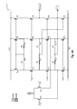
- FIG. 3 shows the voltage regulator 102 with additional detail of offset reduction circuitry 218 in accordance with some embodiments of the present disclosure.
- the offset reduction circuitry 218 may include means for performing offset compensation operations of a first kind and means for performing offset compensation operations of a second kind.
- the means for performing offset compensation operations of a first kind may include sampling switches S 1 -S 8 and capacitors C os and C hold . Each of the sampling switches S 1 -S 8 may be operated in an OPEN state or a CLOSED state in accordance with clock signals (phases) ⁇ 1 and ⁇ 2 .
- the offset reduction circuitry 218 may include a clock generator 302 that is configured to produce ⁇ 1 , ⁇ 2 .
- the sampling switches S 1 -S 8 may be operated by ⁇ 1 , ⁇ 2 to perform an offset compensation operation referred to herein variously as offset sampling, sampling mode, and the like.
- the means for performing offset compensation operations of a first kind may further include Miller compensation to achieve more stable operation of the error amplifier 214 .
- the means for performing offset compensation operations of a first kind may include Miller compensation capacitors (Miller caps) C m1 , C m2 .
- Each Miller cap C m1 , C m2 may be connected to the error amplifier 214 by ⁇ 1 , ⁇ 2 during offset sampling.
- the error amplifier 214 may have a node n casc to which the Miller caps C m1 , C m2 may be connected.
- the means for performing offset compensation operations of a second kind may include input chopping switches Sc 1 -Sc 4 shown in FIG. 3 and output chopping switches Sc 5 -Sc 10 shown in FIG. 3A .
- Each of the input and output chopping switches Sc 1 -Sc 10 may be operated in an OPEN state or a CLOSED state in accordance with ⁇ A and ⁇ B.
- the clock generator 302 may further be configured to produce ⁇ A, ⁇ B.
- the input and output chopping switches Sc 1 -Sc 10 may be operated by ⁇ A, ⁇ B to perform an offset compensation operation referred to herein as “chopping” (chopping operation, etc.).
- Chopping refers to the swapping of the inputs in a , in b of error amplifier 214 concurrently with reversal of the polarity of the output out amp of error amplifier 214 .
- FIG. 4 a simplified example illustrates chopping.
- FIG. 4 shows two circuit configurations. On the left, input A is shown connected to the non-inverting input of amplifier G and input B is shown connected to the inverting input. The output C is shown having a given polarity (e.g., plus). When the amplifier G is chopped, the configuration is changed as shown on the right.
- the inputs are swapped (flipped, reversed, etc.); i.e., input A is now shown connected to the inverting input of amplifier G and input B is shown connected to the non-inverting input.
- the polarity of output C is reversed in order to maintain the proper polarity due to the inputs having been swapped.
- the error amplifier 214 may include an input stage comprising NMOS devices M 1 a , M 2 a , connected to inputs in a , in b respectively.
- the error amplifier 214 may include a folded cascode stage comprising NMOS devices M 2 a , M 2 b , M 3 a , M 3 b , M 4 a , M 4 b , M 5 a , and M 5 b .
- An output stage of error amplifier 214 may include NMOS devices M 6 , M 7 , M 8 , and M 9 to provide the output out amp of error amplifier 214 .
- the output chopping switches Sc 5 -Sc 10 can reverse the polarity at the output out amp .
- FIG. 5 illustrates various timing diagrams showing the relative timing between phases ⁇ 1 , ⁇ 2 , ⁇ A, and ⁇ B in accordance with the present disclosure.
- phase ⁇ 1 may be inverted relative to ⁇ 2 .
- ⁇ 1 is HI
- ⁇ 2 is LO and vice versa; likewise with ⁇ A and ⁇ B.
- a phase is LO
- its corresponding switch may be set to the OPEN state and conversely when a phase is HI, its corresponding switch may be set to the CLOSED state.
- the OPEN/CLOSED convention shown in FIG. 5 can be used herein without loss of generality.
- switches S 1 -S 8 and Sc 1 -Sc 10 may be in the OPEN state when the corresponding phase is LO, and CLOSED when the corresponding phase is HI.
- the error amplifier 214 may operate in sampling mode when ⁇ 1 is HI ( ⁇ 2 LO); e.g., see at time t 0 in FIG. 5 . Conversely, when ⁇ 1 is LO ( ⁇ 2 HI) offset sampling is not active and the error amplifier 214 may operate in regulation mode; e.g., see times t 1 and t 2 . Further in accordance with the present disclosure, chopping may occur at the rising and falling edges of ⁇ A and ⁇ B; e.g., see times t 2 and t 3 .
- FIG. 6 illustrates an example of clock generator 302 shown in FIG. 3 .
- the clock generator 302 may include an oscillator 602 that operates at a frequency of f s .
- a clock generation circuit 604 may receive the output of oscillator 602 to produce phases ⁇ 1 , ⁇ 2 , ⁇ A, and ⁇ B.
- Persons of ordinary skill can implement any suitable circuitry for clock generation circuitry 604 to produce clock signals defined according to the timing diagram shown in FIG. 5 .
- FIG. 7 illustrates the configuration of sampling switches S 1 -S 8 and the configuration of input chopping switches Sc 1 -Sc 4 during sampling mode; e.g., when ⁇ 1 is HI and ⁇ 2 is LO.
- sampling mode coincides with phase ⁇ A, so the input chopping switches Sc 1 and Sc 3 are in the CLOSED state and Sc 2 and Sc 4 are in the OPEN state during sampling mode.
- sampling switches S 1 , S 3 , S 4 , and S 8 are in the CLOSED state and S 2 and S 5 -S 7 are in the OPEN state.
- This configuration of the sampling switches S 1 -S 8 electrically disconnects the error amplifier 214 from the gate of current sense output device M casc , and thus separates control of M casc from error amplifier 214 .
- the voltage V DS across power output device M pass may be connected directly to the non-inverting input in a of error amplifier 214 via sampling switch S 1 , and not through capacitor C os .
- the output out amp of error amplifier 214 may feed back to the inverting input in b of error amplifier 214 via input chopping switch Sc 3 .
- the feedback drives the voltage difference between the drains of M pass and M sense to zero.
- the output out amp of error amplifier 214 will be at a proper voltage level to accommodate that (e.g., on the order of Volts).
- the device components e.g., FIG.
- error amplifier 214 may not be precisely matched; e.g., due to tolerance variations, process variations during fabrication, and so on. Accordingly, a voltage is likely to occur at the output out amp of error amplifier 214 even when the same voltage is applied to the non-inverting and inverting inputs in a , in b . This voltage may be referred to as a DC offset voltage and can manifest itself in the output of error amplifier 214 as a DC level that is added to the output.
- this offset voltage may be stored (sampled) onto capacitor C os via sampling switch S 3 .
- capacitor C os may be implemented using metal insulator metal (MIM) or metal oxide metal (MOM) technology in order to achieve a size suitable for holding an offset voltage (which can be plus or minus) of sufficient magnitude. The size of capacitor C os can determine how often offset sampling must be performed.
- MIM metal insulator metal
- MOM metal oxide metal
- the gate of current sense output device M casc is not driven by the error amplifier 214 during sampling mode because the error amplifier 214 is disconnected from the gate of M casc . Accordingly, the charge stored in capacitor C hold can hold the gate of M casc during sampling mode. The capacitor C hold can therefore prevent the current sense output device M casc from turning OFF during sampling mode. In some embodiments, if ⁇ 1 is sufficiently short in duration, the capacitor C hold can be kept small and thus may be suitable for fabrication using the same technology used to fabricate the voltage regulator 102 .
- FIG. 8 illustrates the configuration of sampling switches S 1 -S 8 and the configuration of input chopping switches Sc 1 -Sc 4 during regulation mode; e.g. when ⁇ 1 is LO and ⁇ 2 is HI.
- the configuration in FIG. 8 shows that ⁇ A is HI and ⁇ B is LO; the input chopping switches Sc 1 -Sc 4 may be said to be in “ ⁇ A state.” Accordingly, Sc 1 and Sc 3 are CLOSED and Sc 2 and Sc 4 are OPEN.
- FIG. 8 shows an example of regulation in the ⁇ A state.
- the error amplifier 214 may operate to control the current sense output device M casc in order to maintain the V DS of sense device M sense equal to the V DS of the power output device M pass .
- V DS of M sense can track V DS of M pass .
- sampling switch S 2 may be CLOSED to connect the V DS of M pass to non-inverting input in a of error amplifier 214 via input chopping switch Sc 1 .
- V DS of M pass is connected to the non-inverting input through capacitor C os .
- capacitor C os stores the offset voltage that was sampled during sampling mode. The voltage on capacitor C os subtractively combines with V DS Of M pass , which effectively reduces the DC offset voltage of error amplifier 214 .
- Sampling switch S 6 may be CLOSED to define a feedback path from the V DS of M sense to the inverting input in b via input chopping switch Sc 3 .
- the output out amp of error amplifier 214 may be connected via sampling switch S 5 to control the gate of current sense output device M casc .
- the Miller cap C m2 may be connected to the output stage of error amplifier 214 ( FIG. 3A ), via sampling switch S 7 , to stabilize its operation.
- FIG. 8A shows the input chopping switches Sc 1 -Sc 4 in a “ ⁇ B state,” where ⁇ A is LO and ⁇ B is HI. Accordingly, Sc 1 and Sc 3 are OPEN and Sc 2 and Sc 4 are CLOSED.
- FIG. 8A shows an example of regulation mode in the ⁇ B state.
- a comparison with FIG. 8 shows that the inputs in a , in b of error amplifier 214 become swapped when chopping occurs. For example, suppose the inputs in a , in b of error amplifier 214 are in the configuration shown in FIG. 8 , namely V DS of M pass is connected to input in a and V DS of M sense is connected to input in b . At time t 2 shown in FIG.
- the inputs in a , in b will be “chopped” (flipped, swapped, etc.) and the configuration will be as shown in FIG. 8A , namely V DS Of M pass is connected to input in b and V DS of M sense is connected to input in a .
- the inputs in a , in b will be chopped again and the configuration will revert to FIG. 8 , and the sequence may repeat at each edge of ⁇ A, ⁇ B.
- FIG. 9 shows internal details of error amplifier 214 with the output chopping switches Sc 5 -Sc 10 that comprise the folded cascode stage in the ⁇ A state.
- the Sc 5 , Sc 8 and Sc 10 switches are CLOSED and Sc 6
- Sc 7 and Sc 9 switches are OPEN.
- An input differential current will be injected to the drain of the fixed bias current mirror of M 5a and M 5b and the sources of the folded cascode devices M 4a and M 4b .
- the current difference of branch of M 5a will be mirrored by the top PMOS mirror M 2a and M 2b .
- the output current will be the summation of M 2b and M 5b , which drives the following common source stage with a fixed bias current from M 6 .
- M 2a and M 2b form a current mirror.
- the signal current through M 2a will be mirrored to M 2b and combine with the signal current through M 4b .
- This signal then drives the common source stage comprising M 9 .
- throwing the current switches does three things: it changes the direction of the current mirroring, it now taps the output signal from the other branch and also feeds the Miller compensation signal to the other cascode device.
- the output chopping switches Sc 5 -Sc 10 in the folded cascode stage are set as shown in the configuration of FIG. 9 .
- the output out amp is referenced to V SS (e.g., ground potential).
- V SS e.g., ground potential
- the output out amp of error amplifier 214 will be chopped in response to the clock edges of ⁇ A, ⁇ B, namely the output chopping switches Sc 5 -Sc 10 will be set as shown in the configuration of FIG. 9A .
- the polarity of output out amp is inverted.
- the output out amp of error amplifier 214 will again be chopped in response to the clock edges of ⁇ A, ⁇ B.
- the output chopping switches Sc 5 -Sc 10 will revert to the configuration of FIG. 9 , and the polarity of output out amp will be restored, and the sequence may repeat at each edge of ⁇ A, ⁇ B.
Landscapes
- Engineering & Computer Science (AREA)
- Physics & Mathematics (AREA)
- Electromagnetism (AREA)
- General Physics & Mathematics (AREA)
- Radar, Positioning & Navigation (AREA)
- Automation & Control Theory (AREA)
- Continuous-Control Power Sources That Use Transistors (AREA)
- Amplifiers (AREA)
Abstract
A voltage regulator having current sense capability may include an input node and an output node. A first output device may be electrically connected between the input node and the output node, and configured to control current flow through the first output device to regulate a voltage at the output node. A current sense circuit may be configured to produce a signal that is indicative of the current through the first output device. The current sense circuit may be configured to perform a first kind of offset compensation operation to reduce an offset voltage in an error amplifier of the current sense circuit, and to perform a second kind of offset compensation operation to reduce the offset voltage in the error amplifier.
Description
Unless otherwise indicated, the foregoing is not admitted to be prior art to the claims recited herein and should not be construed as such.
Manufacturers of electronic devices, especially portable battery powered devices, usually require information about how much power is being consumed by various electronic components in electronic devices. Knowing the amount of current being delivered to a load can be useful in a wide variety of applications. For example, in low-power electronic devices (e.g., smart phone, computer tablets, and other consumer electronics) the supply current can be monitored to understand the system's impact on battery life for purpose of power optimization of the device and end user applications.
Low dropout (LDO) voltage regulators are common in portable electronic devices. Generally, a current sensor is a circuit that can detect a current (e.g., current through a load) and produce an output signal (e.g., current) that is representative of the detected current.
In accordance with some aspects of the present disclosure, a circuit may include an input node and an output node. A first output device may be electrically connected between the input node and the output node. The circuit may include a regulator configured to control current flow through the first output device to regulate a voltage at the output. The circuit may include a current sense circuit configured to produce a signal indicative of the flow of current through the first output device. The current sense circuit may include an error amplifier and a second output device. The error amplifier may be configured to control the second output device to produce the signal indicative of the flow of current through the first output device. The current sense circuit may be further configured to perform a first kind of offset compensation operation to reduce an offset voltage in the error amplifier and to perform a second kind of offset compensation operation different from the first kind of offset compensation operation to also reduce the offset voltage in the error amplifier.
In accordance with some aspects of the present disclosure, a method may include regulating an output voltage at an output node of the circuit. The method may further include sensing a current flow at the output node and generating a control signal in response to the current flow at the output node. The method may include controlling an output device using the control signal to produce a signal indicative of the current flow at the output node. The method may include reducing an offset in the control signal, including performing a first kind of offset compensation operation and performing a second kind of offset compensation operation different from the first kind.
In accordance with some aspects of the present disclosure, a circuit may include means for regulating an output voltage at an output node of the circuit. The circuit may further include means for sensing a current flow at the output node, means for generating a control signal in response to the current flow at the output node, means for producing a signal indicative of the current flow at the output node using the control signal; and means for reducing an offset in the control signal, including means for performing a first kind of offset compensation operation and means for performing a second kind of offset compensation operation different from the first kind.
The following detailed description and accompanying drawings provide a better understanding of the nature and advantages of the present disclosure.
With respect to the discussion to follow and in particular to the drawings, it is stressed that the particulars shown represent examples for purposes of illustrative discussion, and are presented in the cause of providing a description of principles and conceptual aspects of the present disclosure. In this regard, no attempt is made to show implementation details beyond what is needed for a fundamental understanding of the present disclosure. The discussion to follow, in conjunction with the drawings, makes apparent to those of skill in the art how embodiments in accordance with the present disclosure may be practiced. In the accompanying drawings:
In the following description, for purposes of explanation, numerous examples and specific details are set forth in order to provide a thorough understanding of the present disclosure. It will be evident, however, to one skilled in the art that the present disclosure as expressed in the claims may include some or all of the features in these examples, alone or in combination with other features described below, and may further include modifications and equivalents of the features and concepts described herein.
The electronic device 100 may include a voltage regulator 102 to regulate an input voltage Vin to produce a regulated output voltage Vout. In some embodiments, a power source 12 that supplies the input voltage Vin may be internally provided, for example, via a battery. In other embodiments, the power source 12 may be externally provided.
The regulated output voltage Vout may provide power to various device electronics 14 that comprise the electronic device 100. A power monitoring circuit 16 may monitor the power consumption of the device electronics 14. In some embodiments, the power monitoring circuit 16 may be an application processor that can monitor and manage power usage of the device electronics 14. In some embodiments, for example, the voltage regulator 102 may provide a signal Senseout that is indicative of the load current Iload that is flowing into the device electronics 14. The power monitoring circuit 16 may use this information to monitor or otherwise track power consumption of the various subsections that comprise the device electronics, especially where low power consumption is important. The power monitoring circuit 16 may optimize power consumption in the electronic device 100 (e.g., both system functions and end user applications) and maximize battery life (e.g., time before battery is drained). Additionally, in the realm of mobile electronic devices, a main objective may be long battery life. In some other applications (e.g., electronic devices used in server farms) the objective could be minimization of heat and cooling requirements.
The LDO regulator 202 may include a regulator section connected to the power output device Mpass. In some embodiments, the regulator section may include an error amplifier 212 and a feedback path. The error amplifier 212 may have an input (e.g., non-inverting input) connected to a reference voltage Vref, and another input (e.g., inverting input) connected to the feedback path. The feedback path may comprise a resistor divider network, R1, R2 to feed back a portion of the output voltage Vout to the input of error amplifier 212. The portion of the output voltage Vout fed back to amplifier 212 may be compared to reference voltage Vref to produce an output (error signal) to control the gate of power output device Mpass, and hence regulate the output voltage Vout to a value depending on the reference voltage Vref.
The voltage regulator 102 may further include a current sense circuit 204. The current sense circuit 204 may include means for sensing a current flow Iload at the output node 208. In some embodiments, for example, the means for sensing may be a sense device Msense connected to the power output device Mpass in a current mirror configuration. The sense device Msense may be an NMOS device, although a PMOS device may be used in other embodiments. The current through sense device Msense can therefore mirror the current through power output device Mpass. Since sense device Msense serves to indicate current flow, sense device Msense can be made much smaller than power output device Mpass in order to save on circuit area of the voltage regulator 102. Accordingly, the size (e.g., width/length ratio, W/L) of sense device Msense may be several hundreds to thousands of times smaller that the size of power output device Mpass.
The current sense circuit 204 may further include means for producing a signal Senseout that is indicative of the current flow at output node 208. In some embodiments, for example, the means may be a current sense output device Mcasc connected in series with the sense device Msense. The current sense output device Mcasc may be an NMOS device.
In some embodiments, the signal Senseout may be the current Isense through the current sense output device Mcasc. The current Isense flowing through current sense output device Mcasc may be controlled by a control signal 216 at the gate of Mcasc. Means for generating the control signal 216 may include an error amplifier 214 connected to the current sense output device Mcasc. The error amplifier 214 may be configured as a high gain feedback loop to compare the VDS across power output device Mpass and the VDS across sense device Msense to produce an output as control signal 216. Control signal 216 can control the voltage VDS across sense device Msense by controlling the current Isense through the current sense output device Mcasc and hence through Msense.
The error amplifier 214 may have an internal DC offset, for example, due to imperfect matching of the components that comprise the error amplifier 214. Accordingly, the control signal 216 produced by error amplifier 214 can exhibit an offset which can ultimately lead to errors in the signal Senseout. In accordance with the present disclosure, the current sense circuit 204 may further include means for compensating for the offset in control signal 216. In some embodiments, for example, the means may include offset reduction circuitry 218. In accordance with the present disclosure, the offset reduction circuitry 218 may operate at the inputs and the output of error amplifier 214 to reduce the internal DC offset.
As noted above, the voltage regulator 102 in FIG. 2 uses NMOS devices. One of ordinary skill will appreciate that a PMOS version can be easily realized. FIG. 2A shows a voltage regulator 102′ that uses PMOS devices. For discussion purposes, however, the NMOS version shown in FIG. 2 will be used.
In accordance with the present disclosure, the means for performing offset compensation operations of a first kind may further include Miller compensation to achieve more stable operation of the error amplifier 214. Accordingly, in some embodiments the means for performing offset compensation operations of a first kind may include Miller compensation capacitors (Miller caps) Cm1, Cm2. Each Miller cap Cm1, Cm2 may be connected to the error amplifier 214 by ϕ1, ϕ2 during offset sampling. The error amplifier 214 may have a node ncasc to which the Miller caps Cm1, Cm2 may be connected.
Referring to FIGS. 3 and 3A , in some embodiments, the means for performing offset compensation operations of a second kind may include input chopping switches Sc1-Sc4 shown in FIG. 3 and output chopping switches Sc5-Sc10 shown in FIG. 3A . Each of the input and output chopping switches Sc1-Sc10 may be operated in an OPEN state or a CLOSED state in accordance with ϕA and ϕB. The clock generator 302 may further be configured to produce ϕA, ϕB. As will be explained in more detail below, the input and output chopping switches Sc1-Sc10 may be operated by ϕA, ϕB to perform an offset compensation operation referred to herein as “chopping” (chopping operation, etc.).
Chopping refers to the swapping of the inputs ina, inb of error amplifier 214 concurrently with reversal of the polarity of the output outamp of error amplifier 214. Referring for a moment to FIG. 4 , a simplified example illustrates chopping. FIG. 4 shows two circuit configurations. On the left, input A is shown connected to the non-inverting input of amplifier G and input B is shown connected to the inverting input. The output C is shown having a given polarity (e.g., plus). When the amplifier G is chopped, the configuration is changed as shown on the right. The inputs are swapped (flipped, reversed, etc.); i.e., input A is now shown connected to the inverting input of amplifier G and input B is shown connected to the non-inverting input. The polarity of output C is reversed in order to maintain the proper polarity due to the inputs having been swapped. When the amplifier G is chopped again, the configuration reverts to the left side configuration, and so on.
Continuing with FIG. 3A , details of error amplifier 214 in accordance with some embodiments are shown. The error amplifier 214 may include an input stage comprising NMOS devices M1 a, M2 a, connected to inputs ina, inb respectively. The error amplifier 214 may include a folded cascode stage comprising NMOS devices M2 a, M2 b, M3 a, M3 b, M4 a, M4 b, M5 a, and M5 b. An output stage of error amplifier 214 may include NMOS devices M6, M7, M8, and M9 to provide the output outamp of error amplifier 214. As will be shown below, the output chopping switches Sc5-Sc10 can reverse the polarity at the output outamp.
In accordance with the present disclosure, the error amplifier 214 may operate in sampling mode when ϕ1 is HI (ϕ2 LO); e.g., see at time t0 in FIG. 5 . Conversely, when ϕ1 is LO (ϕ2 HI) offset sampling is not active and the error amplifier 214 may operate in regulation mode; e.g., see times t1 and t2. Further in accordance with the present disclosure, chopping may occur at the rising and falling edges of ϕA and ϕB; e.g., see times t2 and t3.
When the error amplifier 214 is in sampling mode, sampling switches S1, S3, S4, and S8 are in the CLOSED state and S2 and S5-S7 are in the OPEN state. This configuration of the sampling switches S1-S8 electrically disconnects the error amplifier 214 from the gate of current sense output device Mcasc, and thus separates control of Mcasc from error amplifier 214.
As shown in FIG. 7 , the voltage VDS across power output device Mpass may be connected directly to the non-inverting input ina of error amplifier 214 via sampling switch S1, and not through capacitor Cos. The output outamp of error amplifier 214 may feed back to the inverting input inb of error amplifier 214 via input chopping switch Sc3. In principle, the feedback drives the voltage difference between the drains of Mpass and Msense to zero. The output outamp of error amplifier 214 will be at a proper voltage level to accommodate that (e.g., on the order of Volts). However, in practice the device components (e.g., FIG. 3A ) that comprise error amplifier 214 may not be precisely matched; e.g., due to tolerance variations, process variations during fabrication, and so on. Accordingly, a voltage is likely to occur at the output outamp of error amplifier 214 even when the same voltage is applied to the non-inverting and inverting inputs ina, inb. This voltage may be referred to as a DC offset voltage and can manifest itself in the output of error amplifier 214 as a DC level that is added to the output.
In accordance with the present disclosure, this offset voltage may be stored (sampled) onto capacitor Cos via sampling switch S3. In some embodiments, capacitor Cos may be implemented using metal insulator metal (MIM) or metal oxide metal (MOM) technology in order to achieve a size suitable for holding an offset voltage (which can be plus or minus) of sufficient magnitude. The size of capacitor Cos can determine how often offset sampling must be performed.
The gate of current sense output device Mcasc is not driven by the error amplifier 214 during sampling mode because the error amplifier 214 is disconnected from the gate of Mcasc. Accordingly, the charge stored in capacitor Chold can hold the gate of Mcasc during sampling mode. The capacitor Chold can therefore prevent the current sense output device Mcasc from turning OFF during sampling mode. In some embodiments, if ϕ1 is sufficiently short in duration, the capacitor Chold can be kept small and thus may be suitable for fabrication using the same technology used to fabricate the voltage regulator 102.
In regulation mode, the error amplifier 214 may operate to control the current sense output device Mcasc in order to maintain the VDS of sense device Msense equal to the VDS of the power output device Mpass. In other words, VDS of Msense can track VDS of Mpass. Accordingly, sampling switch S2 may be CLOSED to connect the VDS of Mpass to non-inverting input ina of error amplifier 214 via input chopping switch Sc1. More particularly, VDS of Mpass is connected to the non-inverting input through capacitor Cos. Recall that capacitor Cos stores the offset voltage that was sampled during sampling mode. The voltage on capacitor Cos subtractively combines with VDS Of Mpass, which effectively reduces the DC offset voltage of error amplifier 214.
Sampling switch S6 may be CLOSED to define a feedback path from the VDS of Msense to the inverting input inb via input chopping switch Sc3. The output outamp of error amplifier 214 may be connected via sampling switch S5 to control the gate of current sense output device Mcasc. The Miller cap Cm2 may be connected to the output stage of error amplifier 214 (FIG. 3A ), via sampling switch S7, to stabilize its operation.
Suppose the output chopping switches Sc5-Sc10 in the folded cascode stage are set as shown in the configuration of FIG. 9 . The output outamp is referenced to VSS (e.g., ground potential). At time t2 (FIG. 5 ), the output outamp of error amplifier 214 will be chopped in response to the clock edges of ϕA, ϕB, namely the output chopping switches Sc5-Sc10 will be set as shown in the configuration of FIG. 9A . The polarity of output outamp is inverted. At time t3, the output outamp of error amplifier 214 will again be chopped in response to the clock edges of ϕA, ϕB. The output chopping switches Sc5-Sc10 will revert to the configuration of FIG. 9 , and the polarity of output outamp will be restored, and the sequence may repeat at each edge of ϕA, ϕB.
The above description illustrates various embodiments of the present disclosure along with examples of how aspects of the particular embodiments may be implemented. The above examples should not be deemed to be the only embodiments, and are presented to illustrate the flexibility and advantages of the particular embodiments as defined by the following claims. Based on the above disclosure and the following claims, other arrangements, embodiments, implementations and equivalents may be employed without departing from the scope of the present disclosure as defined by the claims.
Claims (11)
1. A circuit comprising:
a linear drop-out regulator including a pass transistor and a first error amplifier, wherein an output from the first error amplifier is coupled to a gate of the pass transistor;
a current sense transistor having a source coupled to a source of the pass transistor, wherein the output from the first error amplifier is also coupled to a gate of the current sense transistor;
a current sense output transistor having a source coupled to a drain of the current sense transistor;
a second error amplifier having a first input terminal coupled to a drain of the pass transistor and having a second input terminal coupled to the drain of the current sense transistor, wherein an output of the second error amplifier is coupled to a gate of the current sense output transistor, and wherein a drain of the current sense output transistor is an output current node for the circuit;
offset sampling circuitry configured to compensate for an offset voltage of the second error amplifier with a first kind of offset compensation operation; and
chopping circuitry configured to compensate for the offset voltage of the second error amplifier with a second kind of offset compensation operation.
2. The circuit of claim 1 , wherein inputs of the second error amplifier are swapped and a polarity of the output of the second error amplifier is reversed when the chopping circuitry is configured to perform the second kind of offset compensation operation.
3. The circuit of claim 1 , wherein the circuit further comprises a clock circuit to control a timing between the offset compensation operation of the first kind and the second kind of offset compensation operation.
4. The circuit of claim 1 , wherein the offset sampling circuitry is configured to produce a sample of the offset error and combine the sample with an input to the second error amplifier, and wherein the chopping circuitry is configured to chop inputs to the second error amplifier and the output of the second error amplifier.
5. The circuit of claim 1 , wherein the offset sampling circuitry comprises a plurality of switches, a first capacitor, and a second capacitor, the plurality of switches having a configuration to perform the offset compensation operation of the first kind wherein the plurality of switches:
electrically disconnect the second error amplifier from the first pass transistor;
separate the gate of the current sense output transistor from the second error amplifier;
charge the first capacitor with the offset voltage; and
electrically connect the second capacitor to the gate of the current sense output transistor.
6. The circuit of claim 1 , wherein the chopping circuitry comprises a first plurality of switches electrically connected to inputs of the second error amplifier and configured to swap the inputs and a second plurality of switches electrically connected to the output of the second error amplifier and configured to reverse a polarity of the output of the second error amplifier.
7. The circuit of claim 1 , wherein the circuit further comprises a first compensation capacitor and a second compensation capacitor that are selectively electrically connectable to an output stage of the second error amplifier, the first compensation capacitor being connected to the output stage of the second error amplifier while the first kind of offset compensation operation is performed, the second compensation capacitor being connected to the output stage of the second error amplifier while the first kind of offset compensation operation is not performed.
8. A method comprising:
in a linear drop-out regulator, driving a gate of a pass transistor with an output voltage from a first error amplifier to regulate an output voltage of the linear drop-out regulator;
driving a gate of a current sense transistor with the output voltage from the first error amplifier to conduct a current through the current sense transistor that is combined with a load current from the pass transistor;
producing an output voltage from a second error amplifier responsive to a difference between a drain voltage of the pass transistor and a drain voltage of the current sense transistor;
driving a gate of a current sense output transistor positioned in series with the current sense transistor with the output voltage from the second error amplifier to produce an output current at a drain of the current sense output transistor; and
reducing an offset voltage of the second error amplifier by performing a first kind of offset compensation operation and performing a second kind of offset compensation operation.
9. The method of claim 8 , wherein performing the first kind of offset compensation operation includes sampling the output voltage of the second error amplifier to produce a sampled output, and using the sampled output as an input to the second error amplifier, wherein performing the second kind of offset compensation operation includes swapping connections at inputs of the second error amplifier and reversing polarity of the output voltage of the second error amplifier.
10. The method of claim 8 , further comprising receiving one or more clock signals to control a timing between performing the first kind of offset compensation operation and performing the second kind of offset compensation operation.
11. The method of claim 10 , further comprising using the one or more clock signals to control a plurality of switches to perform the first kind of offset compensation operation and to perform the second kind of offset compensation operation.
Priority Applications (3)
| Application Number | Priority Date | Filing Date | Title |
|---|---|---|---|
| US14/837,308 US10216208B2 (en) | 2015-08-27 | 2015-08-27 | Load current sensing in voltage regulator |
| CN201680049075.6A CN107924207A (en) | 2015-08-27 | 2016-08-12 | Load current sensing in voltage regulator |
| PCT/US2016/046906 WO2017034835A1 (en) | 2015-08-27 | 2016-08-12 | Load current sensing in voltage regulator |
Applications Claiming Priority (1)
| Application Number | Priority Date | Filing Date | Title |
|---|---|---|---|
| US14/837,308 US10216208B2 (en) | 2015-08-27 | 2015-08-27 | Load current sensing in voltage regulator |
Publications (2)
| Publication Number | Publication Date |
|---|---|
| US20170060155A1 US20170060155A1 (en) | 2017-03-02 |
| US10216208B2 true US10216208B2 (en) | 2019-02-26 |
Family
ID=56802688
Family Applications (1)
| Application Number | Title | Priority Date | Filing Date |
|---|---|---|---|
| US14/837,308 Active 2036-07-14 US10216208B2 (en) | 2015-08-27 | 2015-08-27 | Load current sensing in voltage regulator |
Country Status (3)
| Country | Link |
|---|---|
| US (1) | US10216208B2 (en) |
| CN (1) | CN107924207A (en) |
| WO (1) | WO2017034835A1 (en) |
Cited By (2)
| Publication number | Priority date | Publication date | Assignee | Title |
|---|---|---|---|---|
| US11239656B2 (en) * | 2019-07-19 | 2022-02-01 | Texas Instruments Incorporated | Methods and apparatus for current sensing and current limiting |
| US12068743B2 (en) * | 2022-02-21 | 2024-08-20 | Fuji Electric Co., Ltd. | Semiconductor device |
Families Citing this family (4)
| Publication number | Priority date | Publication date | Assignee | Title |
|---|---|---|---|---|
| US9755518B2 (en) * | 2016-02-05 | 2017-09-05 | Qualcomm Incorporated | Current measurments in switching regulators |
| US10873257B2 (en) * | 2018-11-07 | 2020-12-22 | Regents Of The University Of Minnesota | Low dropout regulator with smart offset |
| US11281248B2 (en) * | 2020-02-12 | 2022-03-22 | Nuvoton Technology Corporation | Audio microphone detection using auto-tracking current comparator |
| US11709515B1 (en) * | 2021-07-29 | 2023-07-25 | Dialog Semiconductor (Uk) Limited | Voltage regulator with n-type power switch |
Citations (17)
| Publication number | Priority date | Publication date | Assignee | Title |
|---|---|---|---|---|
| US6201375B1 (en) * | 2000-04-28 | 2001-03-13 | Burr-Brown Corporation | Overvoltage sensing and correction circuitry and method for low dropout voltage regulator |
| US20020158615A1 (en) * | 2000-10-13 | 2002-10-31 | Ryan Goodfellow | System and method for current sensing |
| US20080100276A1 (en) * | 2006-10-30 | 2008-05-01 | Takaaki Negoro | Current sensing circuit and voltage regulator using the same |
| US7518440B1 (en) * | 2007-11-26 | 2009-04-14 | Texas Instruments Incorporated | Dual path chopper stabilized amplifier and method |
| WO2011006979A1 (en) | 2009-07-16 | 2011-01-20 | St-Ericsson (Grenoble) Sas | Low-dropout regulator |
| EP2318660A2 (en) | 2008-07-15 | 2011-05-11 | Stephen Richard Terry | Internal combustion engine |
| US20120038332A1 (en) | 2010-08-10 | 2012-02-16 | Novatek Microelectronics Corp. | Linear voltage regulator and current sensing circuit thereof |
| US20120126760A1 (en) * | 2010-11-19 | 2012-05-24 | Madan Mohan Reddy Vemula | Low dropout regulator |
| US20140103889A1 (en) | 2012-10-11 | 2014-04-17 | Earl W. McCune, Jr. | Rapid-Transition DC-DC Converter |
| US20140217996A1 (en) | 2013-02-06 | 2014-08-07 | Microsemi Corporation | Hysteretic current mode control converter with low, medium and high current thresholds |
| US20140224962A1 (en) | 2013-02-11 | 2014-08-14 | Omnivision Technologies, Inc. | Bandgap reference circuit with offset voltage removal |
| US20150008871A1 (en) * | 2013-07-02 | 2015-01-08 | Stmicroelectronics Design And Application S.R.O. | Method of preventing inversion of output current flow in a voltage regulator and related voltage regulator |
| US20150108842A1 (en) | 2013-10-17 | 2015-04-23 | Qualcomm Incorporated | Systems and methods for reducing cross-supply current |
| US20150115918A1 (en) | 2013-10-25 | 2015-04-30 | Fairchild Semiconductor Corporation | Low drop out supply asymmetric dynamic biasing |
| US20150155780A1 (en) | 2013-12-04 | 2015-06-04 | Apple Inc. | Instantaneous Load Current Monitoring |
| US20160085284A1 (en) * | 2014-09-24 | 2016-03-24 | Rohm Co., Ltd. | Power supply device |
| US20160173041A1 (en) * | 2014-12-11 | 2016-06-16 | Texas Instruments Incorporated | Hot-swap current-sensing system |
Family Cites Families (5)
| Publication number | Priority date | Publication date | Assignee | Title |
|---|---|---|---|---|
| CN101059940A (en) * | 2006-04-18 | 2007-10-24 | 凌阳科技股份有限公司 | Operational Amplifier Driver Circuit to Eliminate Operational Amplifier Offset Voltage |
| US7764215B2 (en) * | 2008-12-31 | 2010-07-27 | Hong Kong Applied Science And Technology Research Institute Co., Ltd. | Multi-stage comparator with offset canceling capacitor across secondary differential inputs for high-speed low-gain compare and high-gain auto-zeroing |
| CN201673425U (en) * | 2010-03-25 | 2010-12-15 | 上海沙丘微电子有限公司 | Low-detuning and low-noise band-gap reference source circuit with stable chopped wave |
| GB201006212D0 (en) * | 2010-04-14 | 2010-06-02 | Rolls Royce Goodrich Engine Co | A signal processing circuit |
| US8841897B2 (en) * | 2011-01-25 | 2014-09-23 | Microchip Technology Incorporated | Voltage regulator having current and voltage foldback based upon load impedance |
-
2015
- 2015-08-27 US US14/837,308 patent/US10216208B2/en active Active
-
2016
- 2016-08-12 CN CN201680049075.6A patent/CN107924207A/en active Pending
- 2016-08-12 WO PCT/US2016/046906 patent/WO2017034835A1/en not_active Ceased
Patent Citations (17)
| Publication number | Priority date | Publication date | Assignee | Title |
|---|---|---|---|---|
| US6201375B1 (en) * | 2000-04-28 | 2001-03-13 | Burr-Brown Corporation | Overvoltage sensing and correction circuitry and method for low dropout voltage regulator |
| US20020158615A1 (en) * | 2000-10-13 | 2002-10-31 | Ryan Goodfellow | System and method for current sensing |
| US20080100276A1 (en) * | 2006-10-30 | 2008-05-01 | Takaaki Negoro | Current sensing circuit and voltage regulator using the same |
| US7518440B1 (en) * | 2007-11-26 | 2009-04-14 | Texas Instruments Incorporated | Dual path chopper stabilized amplifier and method |
| EP2318660A2 (en) | 2008-07-15 | 2011-05-11 | Stephen Richard Terry | Internal combustion engine |
| WO2011006979A1 (en) | 2009-07-16 | 2011-01-20 | St-Ericsson (Grenoble) Sas | Low-dropout regulator |
| US20120038332A1 (en) | 2010-08-10 | 2012-02-16 | Novatek Microelectronics Corp. | Linear voltage regulator and current sensing circuit thereof |
| US20120126760A1 (en) * | 2010-11-19 | 2012-05-24 | Madan Mohan Reddy Vemula | Low dropout regulator |
| US20140103889A1 (en) | 2012-10-11 | 2014-04-17 | Earl W. McCune, Jr. | Rapid-Transition DC-DC Converter |
| US20140217996A1 (en) | 2013-02-06 | 2014-08-07 | Microsemi Corporation | Hysteretic current mode control converter with low, medium and high current thresholds |
| US20140224962A1 (en) | 2013-02-11 | 2014-08-14 | Omnivision Technologies, Inc. | Bandgap reference circuit with offset voltage removal |
| US20150008871A1 (en) * | 2013-07-02 | 2015-01-08 | Stmicroelectronics Design And Application S.R.O. | Method of preventing inversion of output current flow in a voltage regulator and related voltage regulator |
| US20150108842A1 (en) | 2013-10-17 | 2015-04-23 | Qualcomm Incorporated | Systems and methods for reducing cross-supply current |
| US20150115918A1 (en) | 2013-10-25 | 2015-04-30 | Fairchild Semiconductor Corporation | Low drop out supply asymmetric dynamic biasing |
| US20150155780A1 (en) | 2013-12-04 | 2015-06-04 | Apple Inc. | Instantaneous Load Current Monitoring |
| US20160085284A1 (en) * | 2014-09-24 | 2016-03-24 | Rohm Co., Ltd. | Power supply device |
| US20160173041A1 (en) * | 2014-12-11 | 2016-06-16 | Texas Instruments Incorporated | Hot-swap current-sensing system |
Non-Patent Citations (4)
| Title |
|---|
| International Search Report—PCT/US2016/046906—ISA/EPO—dated Nov. 29, 2016. |
| Shi X., et al., "Gain- and offset-compensated non-inverting SC Circuits", Circuits and Systems, 2000. Proceedings. ISCAS 2000 Geneva. The 2000 I EEE International Symposium on May 28-31, 2000, Piscataway, NJ, USA,IEEE, vol. 2, May 28, 2000 (May 28, 2000), pp. 425-428, XP010502751, ISBN: 978-0-7803-5482-1. |
| Written Opinion—PCT/US2016/046906—ISA/EPO—dated Nov. 29, 2016. |
| XIAOJING SHI, MATSUMOTO H., MURAO K.: "Gain- and offset-compensated non-inverting SC circuits", CIRCUITS AND SYSTEMS, 2000. PROCEEDINGS. ISCAS 2000 GENEVA. THE 2000 I EEE INTERNATIONAL SYMPOSIUM ON MAY 28-31, 2000, PISCATAWAY, NJ, USA,IEEE, vol. 2, 28 May 2000 (2000-05-28) - 31 May 2000 (2000-05-31), pages 425 - 428, XP010502751, ISBN: 978-0-7803-5482-1 |
Cited By (2)
| Publication number | Priority date | Publication date | Assignee | Title |
|---|---|---|---|---|
| US11239656B2 (en) * | 2019-07-19 | 2022-02-01 | Texas Instruments Incorporated | Methods and apparatus for current sensing and current limiting |
| US12068743B2 (en) * | 2022-02-21 | 2024-08-20 | Fuji Electric Co., Ltd. | Semiconductor device |
Also Published As
| Publication number | Publication date |
|---|---|
| WO2017034835A1 (en) | 2017-03-02 |
| US20170060155A1 (en) | 2017-03-02 |
| CN107924207A (en) | 2018-04-17 |
Similar Documents
| Publication | Publication Date | Title |
|---|---|---|
| US10216208B2 (en) | Load current sensing in voltage regulator | |
| US9588541B1 (en) | Dual loop regulator circuit | |
| US10873257B2 (en) | Low dropout regulator with smart offset | |
| US7550954B2 (en) | Method and circuit for a voltage supply for real time clock circuitry based on voltage regulated charge pump | |
| US8866341B2 (en) | Voltage regulator | |
| US9223329B2 (en) | Low drop out voltage regulator with operational transconductance amplifier and related method of generating a regulated voltage | |
| US8981739B2 (en) | Low power low dropout linear voltage regulator | |
| US9444414B2 (en) | Current sense circuit using a single opamp having DC offset auto-zeroing | |
| US7598807B2 (en) | Differential amplifier circuit, voltage regulator using the differential amplifier circuit, and method for controlling the differential amplifier circuit | |
| US8284581B2 (en) | Active rectifier and method for energy harvesting power management circuit | |
| TWI785554B (en) | Digital low dropout regulator with fast feedback and optimized frequency response | |
| US20210124383A1 (en) | Techniques for low-dropout (ldo) regulator start-up detection | |
| US11747371B2 (en) | Self-calibrated input voltage-agnostic replica-biased current sensing apparatus | |
| US9146570B2 (en) | Load current compesating output buffer feedback, pass, and sense circuits | |
| US12287659B2 (en) | Low-dropout regulator for low voltage applications | |
| CN1989683A (en) | Low dropout voltage regulator providing adaptive compensation | |
| US20060119421A1 (en) | Regulator circuit | |
| US20160224042A1 (en) | High and low power voltage regulation circuit | |
| US20160231758A1 (en) | Circuit for regulating startup and operation voltage of an electronic device | |
| US11003201B1 (en) | Low quiescent current low-dropout regulator (LDO) | |
| US9235196B2 (en) | Constant voltage circuit and analog electronic clock | |
| US7843183B2 (en) | Real time clock (RTC) voltage regulator and method of regulating an RTC voltage | |
| TWI387179B (en) | Charging circuit capable of improving operational stability | |
| US8981840B1 (en) | Reduction in on-resistance in pass device | |
| Huang et al. | A digital LDO with transient enhancement and limit cycle oscillation reduction |
Legal Events
| Date | Code | Title | Description |
|---|---|---|---|
| AS | Assignment |
Owner name: QUALCOMM INCORPORATED, CALIFORNIA Free format text: ASSIGNMENT OF ASSIGNORS INTEREST;ASSIGNORS:PELUSO, VINCENZO;GUAN, HUA;SIGNING DATES FROM 20150914 TO 20160115;REEL/FRAME:037503/0305 |
|
| STCF | Information on status: patent grant |
Free format text: PATENTED CASE |
|
| MAFP | Maintenance fee payment |
Free format text: PAYMENT OF MAINTENANCE FEE, 4TH YEAR, LARGE ENTITY (ORIGINAL EVENT CODE: M1551); ENTITY STATUS OF PATENT OWNER: LARGE ENTITY Year of fee payment: 4 |