US10203823B2 - Built-in touch display panels basing on organic light emitting devices (OLEDs) - Google Patents
Built-in touch display panels basing on organic light emitting devices (OLEDs) Download PDFInfo
- Publication number
- US10203823B2 US10203823B2 US15/327,779 US201715327779A US10203823B2 US 10203823 B2 US10203823 B2 US 10203823B2 US 201715327779 A US201715327779 A US 201715327779A US 10203823 B2 US10203823 B2 US 10203823B2
- Authority
- US
- United States
- Prior art keywords
- cathode
- blocks
- layer
- cathode blocks
- display panel
- Prior art date
- Legal status (The legal status is an assumption and is not a legal conclusion. Google has not performed a legal analysis and makes no representation as to the accuracy of the status listed.)
- Active, expires
Links
- 239000010409 thin film Substances 0.000 claims abstract description 8
- 230000009189 diving Effects 0.000 claims 1
- 238000004519 manufacturing process Methods 0.000 abstract description 4
- 239000002184 metal Substances 0.000 description 6
- 230000008878 coupling Effects 0.000 description 5
- 238000010168 coupling process Methods 0.000 description 5
- 238000005859 coupling reaction Methods 0.000 description 5
- 238000009413 insulation Methods 0.000 description 5
- 239000000463 material Substances 0.000 description 2
- 238000005516 engineering process Methods 0.000 description 1
- 239000004973 liquid crystal related substance Substances 0.000 description 1
Images


Classifications
-
- G—PHYSICS
- G06—COMPUTING; CALCULATING OR COUNTING
- G06F—ELECTRIC DIGITAL DATA PROCESSING
- G06F3/00—Input arrangements for transferring data to be processed into a form capable of being handled by the computer; Output arrangements for transferring data from processing unit to output unit, e.g. interface arrangements
- G06F3/01—Input arrangements or combined input and output arrangements for interaction between user and computer
- G06F3/03—Arrangements for converting the position or the displacement of a member into a coded form
- G06F3/041—Digitisers, e.g. for touch screens or touch pads, characterised by the transducing means
- G06F3/044—Digitisers, e.g. for touch screens or touch pads, characterised by the transducing means by capacitive means
-
- H—ELECTRICITY
- H10—SEMICONDUCTOR DEVICES; ELECTRIC SOLID-STATE DEVICES NOT OTHERWISE PROVIDED FOR
- H10K—ORGANIC ELECTRIC SOLID-STATE DEVICES
- H10K50/00—Organic light-emitting devices
- H10K50/80—Constructional details
- H10K50/805—Electrodes
- H10K50/82—Cathodes
- H10K50/822—Cathodes characterised by their shape
-
- G—PHYSICS
- G06—COMPUTING; CALCULATING OR COUNTING
- G06F—ELECTRIC DIGITAL DATA PROCESSING
- G06F3/00—Input arrangements for transferring data to be processed into a form capable of being handled by the computer; Output arrangements for transferring data from processing unit to output unit, e.g. interface arrangements
- G06F3/01—Input arrangements or combined input and output arrangements for interaction between user and computer
- G06F3/03—Arrangements for converting the position or the displacement of a member into a coded form
- G06F3/041—Digitisers, e.g. for touch screens or touch pads, characterised by the transducing means
- G06F3/0412—Digitisers structurally integrated in a display
-
- G—PHYSICS
- G06—COMPUTING; CALCULATING OR COUNTING
- G06F—ELECTRIC DIGITAL DATA PROCESSING
- G06F3/00—Input arrangements for transferring data to be processed into a form capable of being handled by the computer; Output arrangements for transferring data from processing unit to output unit, e.g. interface arrangements
- G06F3/01—Input arrangements or combined input and output arrangements for interaction between user and computer
- G06F3/03—Arrangements for converting the position or the displacement of a member into a coded form
- G06F3/041—Digitisers, e.g. for touch screens or touch pads, characterised by the transducing means
- G06F3/044—Digitisers, e.g. for touch screens or touch pads, characterised by the transducing means by capacitive means
- G06F3/0443—Digitisers, e.g. for touch screens or touch pads, characterised by the transducing means by capacitive means using a single layer of sensing electrodes
-
- G—PHYSICS
- G06—COMPUTING; CALCULATING OR COUNTING
- G06F—ELECTRIC DIGITAL DATA PROCESSING
- G06F3/00—Input arrangements for transferring data to be processed into a form capable of being handled by the computer; Output arrangements for transferring data from processing unit to output unit, e.g. interface arrangements
- G06F3/01—Input arrangements or combined input and output arrangements for interaction between user and computer
- G06F3/03—Arrangements for converting the position or the displacement of a member into a coded form
- G06F3/041—Digitisers, e.g. for touch screens or touch pads, characterised by the transducing means
- G06F3/044—Digitisers, e.g. for touch screens or touch pads, characterised by the transducing means by capacitive means
- G06F3/0446—Digitisers, e.g. for touch screens or touch pads, characterised by the transducing means by capacitive means using a grid-like structure of electrodes in at least two directions, e.g. using row and column electrodes
-
- H01L27/323—
-
- H01L27/3276—
-
- H01L51/5221—
-
- H—ELECTRICITY
- H10—SEMICONDUCTOR DEVICES; ELECTRIC SOLID-STATE DEVICES NOT OTHERWISE PROVIDED FOR
- H10K—ORGANIC ELECTRIC SOLID-STATE DEVICES
- H10K50/00—Organic light-emitting devices
- H10K50/80—Constructional details
- H10K50/805—Electrodes
- H10K50/82—Cathodes
-
- H—ELECTRICITY
- H10—SEMICONDUCTOR DEVICES; ELECTRIC SOLID-STATE DEVICES NOT OTHERWISE PROVIDED FOR
- H10K—ORGANIC ELECTRIC SOLID-STATE DEVICES
- H10K59/00—Integrated devices, or assemblies of multiple devices, comprising at least one organic light-emitting element covered by group H10K50/00
- H10K59/10—OLED displays
- H10K59/12—Active-matrix OLED [AMOLED] displays
- H10K59/131—Interconnections, e.g. wiring lines or terminals
-
- H—ELECTRICITY
- H10—SEMICONDUCTOR DEVICES; ELECTRIC SOLID-STATE DEVICES NOT OTHERWISE PROVIDED FOR
- H10K—ORGANIC ELECTRIC SOLID-STATE DEVICES
- H10K59/00—Integrated devices, or assemblies of multiple devices, comprising at least one organic light-emitting element covered by group H10K50/00
- H10K59/40—OLEDs integrated with touch screens
-
- H—ELECTRICITY
- H10—SEMICONDUCTOR DEVICES; ELECTRIC SOLID-STATE DEVICES NOT OTHERWISE PROVIDED FOR
- H10K—ORGANIC ELECTRIC SOLID-STATE DEVICES
- H10K59/00—Integrated devices, or assemblies of multiple devices, comprising at least one organic light-emitting element covered by group H10K50/00
- H10K59/80—Constructional details
- H10K59/805—Electrodes
- H10K59/8051—Anodes
-
- H—ELECTRICITY
- H10—SEMICONDUCTOR DEVICES; ELECTRIC SOLID-STATE DEVICES NOT OTHERWISE PROVIDED FOR
- H10K—ORGANIC ELECTRIC SOLID-STATE DEVICES
- H10K59/00—Integrated devices, or assemblies of multiple devices, comprising at least one organic light-emitting element covered by group H10K50/00
- H10K59/80—Constructional details
- H10K59/805—Electrodes
- H10K59/8052—Cathodes
- H10K59/80521—Cathodes characterised by their shape
-
- G—PHYSICS
- G02—OPTICS
- G02F—OPTICAL DEVICES OR ARRANGEMENTS FOR THE CONTROL OF LIGHT BY MODIFICATION OF THE OPTICAL PROPERTIES OF THE MEDIA OF THE ELEMENTS INVOLVED THEREIN; NON-LINEAR OPTICS; FREQUENCY-CHANGING OF LIGHT; OPTICAL LOGIC ELEMENTS; OPTICAL ANALOGUE/DIGITAL CONVERTERS
- G02F1/00—Devices or arrangements for the control of the intensity, colour, phase, polarisation or direction of light arriving from an independent light source, e.g. switching, gating or modulating; Non-linear optics
- G02F1/01—Devices or arrangements for the control of the intensity, colour, phase, polarisation or direction of light arriving from an independent light source, e.g. switching, gating or modulating; Non-linear optics for the control of the intensity, phase, polarisation or colour
- G02F1/13—Devices or arrangements for the control of the intensity, colour, phase, polarisation or direction of light arriving from an independent light source, e.g. switching, gating or modulating; Non-linear optics for the control of the intensity, phase, polarisation or colour based on liquid crystals, e.g. single liquid crystal display cells
- G02F1/133—Constructional arrangements; Operation of liquid crystal cells; Circuit arrangements
- G02F1/1333—Constructional arrangements; Manufacturing methods
- G02F1/13338—Input devices, e.g. touch panels
-
- G—PHYSICS
- G06—COMPUTING; CALCULATING OR COUNTING
- G06F—ELECTRIC DIGITAL DATA PROCESSING
- G06F2203/00—Indexing scheme relating to G06F3/00 - G06F3/048
- G06F2203/041—Indexing scheme relating to G06F3/041 - G06F3/045
- G06F2203/04103—Manufacturing, i.e. details related to manufacturing processes specially suited for touch sensitive devices
-
- G—PHYSICS
- G06—COMPUTING; CALCULATING OR COUNTING
- G06F—ELECTRIC DIGITAL DATA PROCESSING
- G06F2203/00—Indexing scheme relating to G06F3/00 - G06F3/048
- G06F2203/041—Indexing scheme relating to G06F3/041 - G06F3/045
- G06F2203/04111—Cross over in capacitive digitiser, i.e. details of structures for connecting electrodes of the sensing pattern where the connections cross each other, e.g. bridge structures comprising an insulating layer, or vias through substrate
-
- H01L51/5206—
-
- H—ELECTRICITY
- H10—SEMICONDUCTOR DEVICES; ELECTRIC SOLID-STATE DEVICES NOT OTHERWISE PROVIDED FOR
- H10K—ORGANIC ELECTRIC SOLID-STATE DEVICES
- H10K50/00—Organic light-emitting devices
- H10K50/80—Constructional details
- H10K50/805—Electrodes
- H10K50/81—Anodes
Definitions
- the present disclosure relates to liquid crystal display technology, and more particularly to a built-in touch display panel basing on OLED.
- OLED display panels are not provided with touch function.
- a first metal layer and a second metal layer are arranged on the OLED display panel in sequence.
- the first metal layer and the second metal layer are insulated by an insulation layer, wherein the first metal layer operates as a driving electrode, and the second metal layer operates as a sensing electrode.
- the touch function may be implemented by the driving electrode and the sensing electrode.
- the present disclosure relates to a built-in touch display panel basing on OLED, wherein the touch function may be realized without introducing additional electrode layer and/or the insulation layer.
- a built-in touch display panel basing on organic light emitting displays includes: a thin film transistor (TFT) layer, an anode layer, an OLED layer, and a cathode layer are configured along a bottom-to-up direction; the cathode layer includes a plurality of first cathode blocks and the second cathode blocks, wherein the first cathode blocks and the second cathode blocks are interleaved with each other along a horizontal direction and along a vertical direction of the display panel, the adjacent first cathode blocks are electrically connected, and the adjacent second cathode blocks are electrically connected; wherein the cathode layer further includes a plurality of dividing blocks arranged between the first cathode blocks and the second cathode blocks; and the thin-film transistor (TFT) array layer includes at least one conductive layer, wherein the conductive layer is configured with a plurality of conductive bridges, the adjacent second cathode blocks are electrically connected via the
- cross-sections of the division blocks are reverse-cone-shaped.
- tops of each of the division blocks comprise a specific pattern extending toward the first cathode block and toward another adjacent first cathode block such that the two first cathode blocks are electrically connected on the cathode layer.
- the conductive bridge passes through the anode layer and the OLED layer to contact directly with two corresponding second cathode blocks.
- the conductive bridges are formed by signal lines of the conductive layer.
- cross-sections of the first cathode blocks and the second cathode blocks are rectangular.
- a minimum distance between the adjacent first cathode block and the second cathode block is defined as a sub-pixel distance.
- a built-in touch display panel basing on organic light emitting displays includes: a thin film transistor (TFT) layer, an anode layer, an OLED layer, and a cathode layer are configured along a bottom-to-up direction; the cathode layer includes a plurality of first cathode blocks and the second cathode blocks, wherein the first cathode blocks and the second cathode blocks are interleaved with each other along a horizontal direction and along a vertical direction of the display panel, the adjacent first cathode blocks are electrically connected, and the adjacent second cathode blocks are electrically connected.
- TFT thin film transistor
- OLED organic light emitting display
- the cathode layer further includes a plurality of dividing blocks arranged between the first cathode blocks and the second cathode blocks.
- cross-sections of the division blocks are reverse-cone-shaped.
- tops of each of the division blocks comprise a specific pattern extending toward the first cathode block and toward another adjacent first cathode block such that the two first cathode blocks are electrically connected on the cathode layer.
- the thin-film transistor (TFT) array layer includes at least one conductive layer, wherein the conductive layer is configured with a plurality of conductive bridges, the adjacent second cathode blocks are electrically connected via the corresponding conductive bridges.
- the conductive bridge passes through the anode layer and the OLED layer to contact directly with two corresponding second cathode blocks.
- the conductive bridges are formed by signal lines of the conductive layer.
- cross-sections of the first cathode blocks and the second cathode blocks are rectangular.
- a minimum distance between the adjacent first cathode block and the second cathode block is defined as a sub-pixel distance.
- the cathode layer is divided into a plurality of first cathode blocks and a plurality of second cathode blocks, wherein the first cathode 141 and the second cathode blocks are interleaved with each other along a horizontal direction and along a vertical direction of the display panel.
- the adjacent first cathode blocks are electrically connected to each other, and the adjacent second cathode blocks are electrically connected to each other.
- the touch function may be realized without introducing additional electrode layer and/or the insulation layer.
- the built-in touch display panel basing on OLED may be obtained by simple manufacturing process having the low cost and high yield rate.
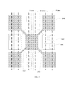
- FIG. 1 is a cross-sectional view of the built-in touch display panel basing on OLED in accordance with one embodiment.
- FIG. 2 is a schematic view of the built-in touch display panel basing on OLED of FIG. 1 .
- FIG. 3 is an enlarged view of the built-in touch display panel basing on OLED of FIG. 2 .
- the display panel is configured with a thin film transistor (TFT) array layer 11 , an anode layer 12 , an OLED layer 13 , and a cathode layer 14 along a bottom-to-up direction.
- TFT thin film transistor
- the cathode layer 14 includes a plurality of first cathode blocks 141 and a plurality of second cathode blocks 142 , wherein the first cathode blocks 141 are insulated from the second cathode blocks 142 .
- the first cathode blocks 141 and the second cathode blocks 142 are interleaved with each other along a horizontal direction and along a vertical direction of the display panel.
- shapes and the dimensions of the cross-sections of the first cathode blocks 141 and the second cathode blocks 142 are the same.
- the shape of the cross-sections of the first cathode blocks 141 and the second cathode blocks 142 are rectangular.
- the cross-sections of the first cathode blocks 141 and the second cathode blocks 142 cover the whole sub-pixel 145 .
- a sub-pixel gap is the minimum distance between the adjacent first cathode block 141 and the second cathode block 142 . In real scenario, the sub-pixel gap is about 10 micrometers. It can be understood that the minimum distance between the adjacent first cathode block 141 and the second cathode block 142 may reach the sub-pixel distance such that the touch precision of the display panel may be enhanced by increasing the density of the first cathode blocks 141 and the second cathode blocks 142 .
- the cathode layer 14 further includes a plurality of division blocks 143 dividing the cathode layer 14 to be the first cathode blocks 141 and the second cathode blocks 142 .
- the division blocks 143 are arranged between the first cathode blocks 141 and the second cathode blocks 142 , and the cross-section of the division blocks 143 are reverse-cone-shaped.
- the division blocks 143 may be of the shape other than the reverse-cone-shaped.
- the adjacent first cathode blocks 141 electrically connect to each other.
- four division blocks 143 are configured to surround the first cathode block 141 .
- the four division blocks 143 are arranged at four corners of the first cathode block 141 .
- the first cathode block 141 electrically connects to four adjacent first cathode blocks 141 via the four division blocks 143 .
- Tops of each of the division blocks 143 include a specific pattern extending toward one corner of the first cathode blocks 141 and the closest corner of another first cathode block 141 such that the two first cathode blocks 141 are electrically connected on the cathode layer 14 .
- the adjacent second cathode blocks 142 are electrically connected.
- the TFT array layer 11 includes at least one conductive layer 111 , wherein the conductive layer 111 is configured with a plurality of conductive bridges 112 .
- the adjacent second cathode blocks 142 are electrically connected via the corresponding conductive bridges 112 .
- the conductive bridge 112 passes through the anode layer 12 and the OLED layer 13 to contact directly with two corresponding second cathode blocks 142 .
- the conductive bridges 112 are not covered by the anode layer 12 and the OLED layer 13 .
- the anode layer 12 is divided into a plurality of anode blocks 121 by the conductive bridges 112 , and the anode blocks 121 are spaced apart from each other.
- the OLED layer 13 is divided into a plurality of OLED blocks 131 by the conductive bridges 112 , and the OLED blocks 131 are spaced apart from each other.
- the conductive bridges 112 pass through the gap between the anode blocks 121 and the gap between the OLED blocks 131 to directly contact with the two corresponding second cathode blocks 142 .
- four conductive bridges 112 are configured to surround one second cathode block 142 .
- the second cathode blocks 142 is rectangular-shaped, four conductive bridges 112 are arranged at four corners of the second cathode blocks 142 .
- One end of the four conductive bridges 112 connects to four corners of the second cathode blocks 142 .
- the other end of the four conductive bridges 112 respectively connects to the four closest corners of other adjacent second cathode blocks 142 such that the adjacent second cathode blocks 142 are electrically connected on the conductive layer 111 .
- the conductive bridges 112 are formed by signal lines (S-Line) of the conductive layer 111 of the TFT array layer 11 , wherein the signal lines (S-Line) are made by SD materials.
- the data lines (D-Line) and power lines (P-Line) on the same conductive layer 111 detour with respect to the conductive bridges 112 . That is, the data lines (D-Line) and power lines (P-Line) surround the conductive bridges 112 .
- the first cathode block 141 is a driving electrode
- the second cathode block 142 is a sensing electrode
- the first cathode block 141 may be the sensing electrode
- the second cathode block 142 may be the driving electrode
- the display function and the touch function of the display panel are executed on different time, wherein the TFT array layer 11 , the anode layer 12 , the OLED layer 13 , and the cathode layer 14 cooperatively operate with each other to display images.
- the TFT array layer 11 , the anode layer 12 , the OLED layer 13 , and the cathode layer 14 display the images according to image display data in response to the control signals.
- the cathode layer 14 is configured to sense the touch.
- the coupling between the first cathode blocks 141 and the second cathode blocks 142 close to the pressed point may be affected, that is, the coupling between the sensing electrode and the driving electrode may be affected, i.e., the amount of the coupling capacitance.
- the sensing electrode issues a triggering signals, and the scanning electrode receives the signals one by one. In this way, all of the coupling capacitance between the driving electrode and the sensing electrode may be obtained.
- the coordination of the pressed point may be obtained by comparing the changed amount of the coupling capacitance so as to realize the touch function.
- the cathode layer is divided into a plurality of first cathode blocks and a plurality of second cathode blocks, wherein the first cathode blocks 141 and the second cathode blocks are interleaved with each other along a horizontal direction and along a vertical direction of the display panel.
- the adjacent first cathode blocks are electrically connected to each other, and the adjacent second cathode blocks are electrically connected to each other.
- the touch function may be realized without introducing additional electrode layer and/or the insulation layer.
- the built-in touch display panel basing on OLED may be obtained by simple manufacturing process having the low cost and high yield rate.
Abstract
The present disclosure relates to a built-in touch display panel basing on OLED includes: a thin film transistor (TFT) layer, an anode layer, an OLED layer, and a cathode layer are configured along a bottom-to-up direction; and the cathode layer includes a plurality of first cathode blocks and the second cathode blocks, wherein the first cathode blocks and the second cathode blocks are interleaved with each other along a horizontal direction and along a vertical direction of the display panel, the adjacent first cathode blocks are electrically connected, and the adjacent second cathode blocks are electrically connected. In this way, the built-in touch display panel basing on OLED may be obtained by simple manufacturing process having the low cost and high yield rate.
Description
1. Field of the Invention
The present disclosure relates to liquid crystal display technology, and more particularly to a built-in touch display panel basing on OLED.
2. Discussion of the Related Art
Conventionally, Organic Light Emitting Display (OLED) display panels are not provided with touch function. To enable the touch function, a first metal layer and a second metal layer are arranged on the OLED display panel in sequence. The first metal layer and the second metal layer are insulated by an insulation layer, wherein the first metal layer operates as a driving electrode, and the second metal layer operates as a sensing electrode. The touch function may be implemented by the driving electrode and the sensing electrode.
However, when the touch function is realized by the conventional solution, additional electrode layers and the insulation layer are configured, which results in higher cost, more complicated manufacturing process, and lower yield rate.
The present disclosure relates to a built-in touch display panel basing on OLED, wherein the touch function may be realized without introducing additional electrode layer and/or the insulation layer.
In one aspect, a built-in touch display panel basing on organic light emitting displays (OLEDs) includes: a thin film transistor (TFT) layer, an anode layer, an OLED layer, and a cathode layer are configured along a bottom-to-up direction; the cathode layer includes a plurality of first cathode blocks and the second cathode blocks, wherein the first cathode blocks and the second cathode blocks are interleaved with each other along a horizontal direction and along a vertical direction of the display panel, the adjacent first cathode blocks are electrically connected, and the adjacent second cathode blocks are electrically connected; wherein the cathode layer further includes a plurality of dividing blocks arranged between the first cathode blocks and the second cathode blocks; and the thin-film transistor (TFT) array layer includes at least one conductive layer, wherein the conductive layer is configured with a plurality of conductive bridges, the adjacent second cathode blocks are electrically connected via the corresponding conductive bridges.
Wherein cross-sections of the division blocks are reverse-cone-shaped.
Wherein tops of each of the division blocks comprise a specific pattern extending toward the first cathode block and toward another adjacent first cathode block such that the two first cathode blocks are electrically connected on the cathode layer.
Wherein the conductive bridge passes through the anode layer and the OLED layer to contact directly with two corresponding second cathode blocks.
Wherein the conductive bridges are formed by signal lines of the conductive layer.
Wherein shapes and the dimensions of the cross-sections of the first cathode blocks and the second cathode blocks are the same.
Wherein cross-sections of the first cathode blocks and the second cathode blocks are rectangular.
Wherein a minimum distance between the adjacent first cathode block and the second cathode block is defined as a sub-pixel distance.
In another aspect, a built-in touch display panel basing on organic light emitting displays (OLEDs) includes: a thin film transistor (TFT) layer, an anode layer, an OLED layer, and a cathode layer are configured along a bottom-to-up direction; the cathode layer includes a plurality of first cathode blocks and the second cathode blocks, wherein the first cathode blocks and the second cathode blocks are interleaved with each other along a horizontal direction and along a vertical direction of the display panel, the adjacent first cathode blocks are electrically connected, and the adjacent second cathode blocks are electrically connected.
Wherein the cathode layer further includes a plurality of dividing blocks arranged between the first cathode blocks and the second cathode blocks.
Wherein cross-sections of the division blocks are reverse-cone-shaped.
Wherein tops of each of the division blocks comprise a specific pattern extending toward the first cathode block and toward another adjacent first cathode block such that the two first cathode blocks are electrically connected on the cathode layer.
Wherein the thin-film transistor (TFT) array layer includes at least one conductive layer, wherein the conductive layer is configured with a plurality of conductive bridges, the adjacent second cathode blocks are electrically connected via the corresponding conductive bridges.
Wherein the conductive bridge passes through the anode layer and the OLED layer to contact directly with two corresponding second cathode blocks.
Wherein the conductive bridges are formed by signal lines of the conductive layer.
Wherein shapes and the dimensions of the cross-sections of the first cathode blocks and the second cathode blocks are the same.
Wherein cross-sections of the first cathode blocks and the second cathode blocks are rectangular.
Wherein a minimum distance between the adjacent first cathode block and the second cathode block is defined as a sub-pixel distance.
In view of the above, the cathode layer is divided into a plurality of first cathode blocks and a plurality of second cathode blocks, wherein the first cathode 141 and the second cathode blocks are interleaved with each other along a horizontal direction and along a vertical direction of the display panel. The adjacent first cathode blocks are electrically connected to each other, and the adjacent second cathode blocks are electrically connected to each other. In this way, the touch function may be realized without introducing additional electrode layer and/or the insulation layer. In addition, the built-in touch display panel basing on OLED may be obtained by simple manufacturing process having the low cost and high yield rate.
Embodiments of the invention will now be described more fully hereinafter with reference to the accompanying drawings, in which embodiments of the invention are shown.
As shown in FIGS. 1-3 , the display panel is configured with a thin film transistor (TFT) array layer 11, an anode layer 12, an OLED layer 13, and a cathode layer 14 along a bottom-to-up direction.
The cathode layer 14 includes a plurality of first cathode blocks 141 and a plurality of second cathode blocks 142, wherein the first cathode blocks 141 are insulated from the second cathode blocks 142. The first cathode blocks 141 and the second cathode blocks 142 are interleaved with each other along a horizontal direction and along a vertical direction of the display panel. Preferably, shapes and the dimensions of the cross-sections of the first cathode blocks 141 and the second cathode blocks 142 are the same.
In the embodiment, the shape of the cross-sections of the first cathode blocks 141 and the second cathode blocks 142 are rectangular. The cross-sections of the first cathode blocks 141 and the second cathode blocks 142 cover the whole sub-pixel 145. A sub-pixel gap is the minimum distance between the adjacent first cathode block 141 and the second cathode block 142. In real scenario, the sub-pixel gap is about 10 micrometers. It can be understood that the minimum distance between the adjacent first cathode block 141 and the second cathode block 142 may reach the sub-pixel distance such that the touch precision of the display panel may be enhanced by increasing the density of the first cathode blocks 141 and the second cathode blocks 142.
Preferably, the cathode layer 14 further includes a plurality of division blocks 143 dividing the cathode layer 14 to be the first cathode blocks 141 and the second cathode blocks 142. In the embodiment, the division blocks 143 are arranged between the first cathode blocks 141 and the second cathode blocks 142, and the cross-section of the division blocks 143 are reverse-cone-shaped. In other embodiments, the division blocks 143 may be of the shape other than the reverse-cone-shaped.
In the embodiment, the adjacent first cathode blocks 141 electrically connect to each other. Specifically, in addition to the edge portions of the display panel, four division blocks 143 are configured to surround the first cathode block 141. Preferably, when the first cathode block 141 is rectangular-shaped, the four division blocks 143 are arranged at four corners of the first cathode block 141. The first cathode block 141 electrically connects to four adjacent first cathode blocks 141 via the four division blocks 143. Tops of each of the division blocks 143 include a specific pattern extending toward one corner of the first cathode blocks 141 and the closest corner of another first cathode block 141 such that the two first cathode blocks 141 are electrically connected on the cathode layer 14.
In the embodiment, the adjacent second cathode blocks 142 are electrically connected. The TFT array layer 11 includes at least one conductive layer 111, wherein the conductive layer 111 is configured with a plurality of conductive bridges 112. The adjacent second cathode blocks 142 are electrically connected via the corresponding conductive bridges 112. Preferably, the conductive bridge 112 passes through the anode layer 12 and the OLED layer 13 to contact directly with two corresponding second cathode blocks 142. In another aspect, the conductive bridges 112 are not covered by the anode layer 12 and the OLED layer 13. That is, the anode layer 12 is divided into a plurality of anode blocks 121 by the conductive bridges 112, and the anode blocks 121 are spaced apart from each other. The OLED layer 13 is divided into a plurality of OLED blocks 131 by the conductive bridges 112, and the OLED blocks 131 are spaced apart from each other. The conductive bridges 112 pass through the gap between the anode blocks 121 and the gap between the OLED blocks 131 to directly contact with the two corresponding second cathode blocks 142.
In the embodiment, in addition to the edge portion of the display panel, four conductive bridges 112 are configured to surround one second cathode block 142. Preferably, when the second cathode blocks 142 is rectangular-shaped, four conductive bridges 112 are arranged at four corners of the second cathode blocks 142. One end of the four conductive bridges 112 connects to four corners of the second cathode blocks 142. The other end of the four conductive bridges 112 respectively connects to the four closest corners of other adjacent second cathode blocks 142 such that the adjacent second cathode blocks 142 are electrically connected on the conductive layer 111.
Preferably, when the display panel is the OLED display panel of a top-gate type, the conductive bridges 112 are formed by signal lines (S-Line) of the conductive layer 111 of the TFT array layer 11, wherein the signal lines (S-Line) are made by SD materials. In addition, to avoid short connections, the data lines (D-Line) and power lines (P-Line) on the same conductive layer 111 detour with respect to the conductive bridges 112. That is, the data lines (D-Line) and power lines (P-Line) surround the conductive bridges 112.
In the embodiment, the first cathode block 141 is a driving electrode, and the second cathode block 142 is a sensing electrode. In other embodiment, the first cathode block 141 may be the sensing electrode, and the second cathode block 142 may be the driving electrode.
In real scenarios, the display function and the touch function of the display panel are executed on different time, wherein the TFT array layer 11, the anode layer 12, the OLED layer 13, and the cathode layer 14 cooperatively operate with each other to display images. Specifically, before the displayed time arrives, the TFT array layer 11, the anode layer 12, the OLED layer 13, and the cathode layer 14 display the images according to image display data in response to the control signals. The cathode layer 14 is configured to sense the touch. Specifically, when fingers of the user press the display panel, the coupling between the first cathode blocks 141 and the second cathode blocks 142 close to the pressed point may be affected, that is, the coupling between the sensing electrode and the driving electrode may be affected, i.e., the amount of the coupling capacitance. When the displayed time arrives, the sensing electrode issues a triggering signals, and the scanning electrode receives the signals one by one. In this way, all of the coupling capacitance between the driving electrode and the sensing electrode may be obtained. The coordination of the pressed point may be obtained by comparing the changed amount of the coupling capacitance so as to realize the touch function.
In view of the above, the cathode layer is divided into a plurality of first cathode blocks and a plurality of second cathode blocks, wherein the first cathode blocks 141 and the second cathode blocks are interleaved with each other along a horizontal direction and along a vertical direction of the display panel. The adjacent first cathode blocks are electrically connected to each other, and the adjacent second cathode blocks are electrically connected to each other. In this way, the touch function may be realized without introducing additional electrode layer and/or the insulation layer. In addition, the built-in touch display panel basing on OLED may be obtained by simple manufacturing process having the low cost and high yield rate.
It is believed that the present embodiments and their advantages will be understood from the foregoing description, and it will be apparent that various changes may be made thereto without departing from the spirit and scope of the invention or sacrificing all of its material advantages, the examples hereinbefore described merely being preferred or exemplary embodiments of the invention.
Claims (6)
1. A built-in touch display panel based on organic light emitting displays (OLEDs), comprising:
a thin film transistor (TFT) layer, an anode layer, an OLED layer, and a cathode layer are configured sequentially along a bottom-to-up direction and cooperatively operate with each other to display images;
the cathode layer comprises a plurality of first cathode blocks and a plurality of second cathode blocks, wherein the first cathode blocks and the second cathode blocks are interleaved with each other along a horizontal direction and along a vertical direction of the display panel, the adjacent first cathode blocks are electrically connected, and the adjacent second cathode blocks are electrically connected;
the first cathode block are driving electrodes and the second cathode blocks are sensing electrodes or the second cathode blocks are driving eletrodes and the first cathode blocks are sensing electodes, so as to perform a touch function of the display panel;
wherein the cathode layer further comprises a plurality of dividing blocks arranged between the first cathode blocks and the second cathode blocks, and cross-sections of the dividing blocks are reverse-cone-shaped;
the thin-film transistor (TFT) array layer comprises at least one conductive layer, wherein the conductive layer is configured with a plurality of conductive bridges, the adjacent second cathode blocks are electrically connected via the corresponding conductive bridges;
wherein four dividing blocks are arranged at four corners of each of the first cathode blocks, and each of the first cathode blocks electrically connects to four adjacent first cathode blocks via the four diving blocks; and
wherein each of the four dividing blocks comprises a specific pattern extending toward one of the cathode blocks and toward another adjacent first cathode block such that both the first cathode blocks are electrically connected on the cathode layer.
2. The display panel as claimed in claim 1 , wherein each conductive bridge passes through the anode layer and the OLED layer to contact directly with two corresponding second cathode blocks.
3. The display panel as claimed in claim 2 , wherein the conductive bridges are formed by signal lines of the conductive layer.
4. The display panel as claimed in claim 1 , wherein shapes and the dimensions of the cross-sections of the first cathode blocks and the second cathode blocks are the same.
5. The display panel as claimed in claim 4 , wherein cross-sections of the first cathode blocks and the second cathode blocks are rectangular.
6. The display panel as claimed in claim 5 , wherein a minimum distance between the adjacent first cathode block and the second cathode block is defined as a sub-pixel distance.
Applications Claiming Priority (3)
| Application Number | Priority Date | Filing Date | Title |
|---|---|---|---|
| CN2016112182955 | 2016-12-26 | ||
| CN201611218295.5A CN106653813B (en) | 2016-12-26 | 2016-12-26 | A kind of built-in touch-control display panel based on OLED |
| PCT/CN2017/070522 WO2018120287A1 (en) | 2016-12-26 | 2017-01-07 | Oled-based built-in touch display panel |
Publications (2)
| Publication Number | Publication Date |
|---|---|
| US20180211998A1 US20180211998A1 (en) | 2018-07-26 |
| US10203823B2 true US10203823B2 (en) | 2019-02-12 |
Family
ID=58828367
Family Applications (1)
| Application Number | Title | Priority Date | Filing Date |
|---|---|---|---|
| US15/327,779 Active 2037-07-31 US10203823B2 (en) | 2016-12-26 | 2017-01-07 | Built-in touch display panels basing on organic light emitting devices (OLEDs) |
Country Status (3)
| Country | Link |
|---|---|
| US (1) | US10203823B2 (en) |
| CN (1) | CN106653813B (en) |
| WO (1) | WO2018120287A1 (en) |
Families Citing this family (8)
| Publication number | Priority date | Publication date | Assignee | Title |
|---|---|---|---|---|
| CN107482128A (en) * | 2017-07-25 | 2017-12-15 | 武汉华星光电半导体显示技术有限公司 | A kind of touch-control array base palte and contact panel |
| CN108255347B (en) * | 2018-01-26 | 2020-06-30 | 云谷(固安)科技有限公司 | Touch display panel and preparation method and driving method thereof |
| CN109189268B (en) * | 2018-09-12 | 2019-12-17 | 武汉华星光电半导体显示技术有限公司 | Organic light emitting diode touch panel and method of forming the same |
| KR20200082355A (en) | 2018-12-28 | 2020-07-08 | 엘지디스플레이 주식회사 | Touch display |
| CN110767831B (en) * | 2018-12-28 | 2022-10-04 | 昆山国显光电有限公司 | Transparent OLED substrate, display panel, array substrate, display screen and display device |
| KR20200102025A (en) | 2019-02-20 | 2020-08-31 | 삼성디스플레이 주식회사 | Display device |
| CN110096175B (en) * | 2019-04-23 | 2023-06-27 | 武汉华星光电半导体显示技术有限公司 | Display panel |
| KR20210009479A (en) | 2019-07-16 | 2021-01-27 | 삼성디스플레이 주식회사 | Display apparatus, apparatus and method for manufacturing the same |
Citations (13)
| Publication number | Priority date | Publication date | Assignee | Title |
|---|---|---|---|---|
| CN102541333A (en) | 2010-12-30 | 2012-07-04 | 上海天马微电子有限公司 | In-cell touch screen |
| US20140253502A1 (en) * | 2013-03-07 | 2014-09-11 | Samsung Display Co., Ltd. | Display device integrated with touch screen panel and driving method thereof |
| CN104409469A (en) | 2014-10-30 | 2015-03-11 | 京东方科技集团股份有限公司 | AMOLED touch control display device, and preparation method and drive method thereof |
| US20160111481A1 (en) * | 2014-10-21 | 2016-04-21 | Samsung Display Co., Ltd. | Organic light-emitting diode display |
| US20160252996A1 (en) | 2014-09-16 | 2016-09-01 | Boe Technology Group Co., Ltd. | Array substrate, in-cell touch screen and touch display device |
| US20160291790A1 (en) * | 2015-04-01 | 2016-10-06 | Shanghai Tianma Micro-electronics Co., Ltd. | Touch display panel and touch display device |
| US20170003800A1 (en) * | 2013-12-27 | 2017-01-05 | Kunshan New Flat Panel Display Technology Center Co., Ltd. | Touch control display device and a preparation method thereof |
| US20170010734A1 (en) * | 2014-11-28 | 2017-01-12 | Boe Technology Group Co., Ltd. | Pixel Structure, Transparent Touch Display Screen and Manufacturing Method Thereof, and Display Device |
| US20170075452A1 (en) * | 2015-09-10 | 2017-03-16 | Samsung Display Co., Ltd. | Display device with touch screen and method for manufacturing the display device |
| US20170090634A1 (en) * | 2015-09-24 | 2017-03-30 | Lg Display Co., Ltd. | Display device including touch screen function |
| US20170329443A1 (en) * | 2015-08-27 | 2017-11-16 | Boe Technology Group Co., Ltd. | Oled array substrate, manufacturing method thereof and touch display device |
| US20180059869A1 (en) * | 2016-08-31 | 2018-03-01 | Japan Display Inc. | Touch sensor and touch screen |
| US20180095566A1 (en) * | 2016-09-30 | 2018-04-05 | Lg Display Co., Ltd. | Display Device with Touch Sensor |
-
2016
- 2016-12-26 CN CN201611218295.5A patent/CN106653813B/en active Active
-
2017
- 2017-01-07 US US15/327,779 patent/US10203823B2/en active Active
- 2017-01-07 WO PCT/CN2017/070522 patent/WO2018120287A1/en active Application Filing
Patent Citations (13)
| Publication number | Priority date | Publication date | Assignee | Title |
|---|---|---|---|---|
| CN102541333A (en) | 2010-12-30 | 2012-07-04 | 上海天马微电子有限公司 | In-cell touch screen |
| US20140253502A1 (en) * | 2013-03-07 | 2014-09-11 | Samsung Display Co., Ltd. | Display device integrated with touch screen panel and driving method thereof |
| US20170003800A1 (en) * | 2013-12-27 | 2017-01-05 | Kunshan New Flat Panel Display Technology Center Co., Ltd. | Touch control display device and a preparation method thereof |
| US20160252996A1 (en) | 2014-09-16 | 2016-09-01 | Boe Technology Group Co., Ltd. | Array substrate, in-cell touch screen and touch display device |
| US20160111481A1 (en) * | 2014-10-21 | 2016-04-21 | Samsung Display Co., Ltd. | Organic light-emitting diode display |
| CN104409469A (en) | 2014-10-30 | 2015-03-11 | 京东方科技集团股份有限公司 | AMOLED touch control display device, and preparation method and drive method thereof |
| US20170010734A1 (en) * | 2014-11-28 | 2017-01-12 | Boe Technology Group Co., Ltd. | Pixel Structure, Transparent Touch Display Screen and Manufacturing Method Thereof, and Display Device |
| US20160291790A1 (en) * | 2015-04-01 | 2016-10-06 | Shanghai Tianma Micro-electronics Co., Ltd. | Touch display panel and touch display device |
| US20170329443A1 (en) * | 2015-08-27 | 2017-11-16 | Boe Technology Group Co., Ltd. | Oled array substrate, manufacturing method thereof and touch display device |
| US20170075452A1 (en) * | 2015-09-10 | 2017-03-16 | Samsung Display Co., Ltd. | Display device with touch screen and method for manufacturing the display device |
| US20170090634A1 (en) * | 2015-09-24 | 2017-03-30 | Lg Display Co., Ltd. | Display device including touch screen function |
| US20180059869A1 (en) * | 2016-08-31 | 2018-03-01 | Japan Display Inc. | Touch sensor and touch screen |
| US20180095566A1 (en) * | 2016-09-30 | 2018-04-05 | Lg Display Co., Ltd. | Display Device with Touch Sensor |
Also Published As
| Publication number | Publication date |
|---|---|
| US20180211998A1 (en) | 2018-07-26 |
| CN106653813B (en) | 2019-01-22 |
| CN106653813A (en) | 2017-05-10 |
| WO2018120287A1 (en) | 2018-07-05 |
Similar Documents
| Publication | Publication Date | Title |
|---|---|---|
| US10203823B2 (en) | Built-in touch display panels basing on organic light emitting devices (OLEDs) | |
| US11960669B2 (en) | Display device including touch screen function | |
| US10345978B2 (en) | In-cell touch display panel | |
| US9823766B2 (en) | Array substrate and display device | |
| US10168593B2 (en) | Liquid crystal display panel having dual capacitors connected in parallel to shift register unit and array substrate thereof | |
| US10579173B2 (en) | Touch display panel and driving method thereof and touch display device | |
| CN109557728B (en) | Pixel structure, manufacturing method thereof, array substrate and touch display device | |
| US9224762B1 (en) | Array substrate and display device | |
| US10466820B2 (en) | OLED array substrate, manufacturing method thereof and touch display device | |
| US20180292693A1 (en) | A display panel and an array substrate thereof | |
| US9817503B2 (en) | Thin film transistor substrate and in-cell touch display panel using same | |
| US10001860B2 (en) | Touch display panel, fabricating method thereof and driving method thereof | |
| US20180233550A1 (en) | Transparent oled display panel | |
| US20180157135A1 (en) | Pixel structure, array substrate, and liquid crystal display panel | |
| US20170205955A1 (en) | Touch display panel and driving method therefor, and display device | |
| US10748940B2 (en) | TFT substrate having data lines as touch driving electrode and common electrodes as touch sensing electrode and touch display panel using same | |
| US9213441B2 (en) | In-cell touch panel and liquid crystal device | |
| US11669180B2 (en) | Touch display substrate and display device | |
| US20150378228A1 (en) | Array substrate and liquid crystal display device | |
| US10061436B2 (en) | Touch display panel, driving method and touch display device | |
| US10658394B2 (en) | Array substrate and manufacturing method thereof, display panel and display device | |
| US9563301B2 (en) | Array substrate, fabricating method thereof and display device | |
| US11538835B2 (en) | Array substrate with dummy lead including disconnected conducting wires, method for manufacturing the same, display panel and display device | |
| JP2013140366A (en) | Tft array substrate | |
| US20190317371A1 (en) | Liquid crystal grating and fabrication method thereof, and display device |
Legal Events
| Date | Code | Title | Description |
|---|---|---|---|
| AS | Assignment |
Owner name: WUHAN CHINA STAR OPTOELECTRONICS TECHNOLOGY CO., L Free format text: ASSIGNMENT OF ASSIGNORS INTEREST;ASSIGNORS:HIDEO, HIRAYAMA;HAJIME, NAGAI;SIGNING DATES FROM 20170105 TO 20170109;REEL/FRAME:041025/0790 |
|
| STCF | Information on status: patent grant |
Free format text: PATENTED CASE |
|
| MAFP | Maintenance fee payment |
Free format text: PAYMENT OF MAINTENANCE FEE, 4TH YEAR, LARGE ENTITY (ORIGINAL EVENT CODE: M1551); ENTITY STATUS OF PATENT OWNER: LARGE ENTITY Year of fee payment: 4 |