US10193593B2 - Signal processing device, communication system, and signal processing method - Google Patents
Signal processing device, communication system, and signal processing method Download PDFInfo
- Publication number
- US10193593B2 US10193593B2 US15/753,694 US201615753694A US10193593B2 US 10193593 B2 US10193593 B2 US 10193593B2 US 201615753694 A US201615753694 A US 201615753694A US 10193593 B2 US10193593 B2 US 10193593B2
- Authority
- US
- United States
- Prior art keywords
- unit
- signal
- fourier transform
- basis
- equalization
- Prior art date
- Legal status (The legal status is an assumption and is not a legal conclusion. Google has not performed a legal analysis and makes no representation as to the accuracy of the status listed.)
- Active
Links
- 238000012545 processing Methods 0.000 title claims description 64
- 238000004891 communication Methods 0.000 title claims description 36
- 238000003672 processing method Methods 0.000 title claims description 10
- 230000003287 optical effect Effects 0.000 claims abstract description 97
- 239000011159 matrix material Substances 0.000 claims abstract description 82
- 230000005540 biological transmission Effects 0.000 claims abstract description 29
- 239000006185 dispersion Substances 0.000 claims abstract description 21
- 238000000034 method Methods 0.000 claims description 59
- 230000010287 polarization Effects 0.000 claims description 8
- 230000008054 signal transmission Effects 0.000 claims description 7
- 230000007274 generation of a signal involved in cell-cell signaling Effects 0.000 claims description 6
- 238000004364 calculation method Methods 0.000 abstract description 22
- 238000012546 transfer Methods 0.000 abstract description 16
- 238000010586 diagram Methods 0.000 description 16
- 238000006243 chemical reaction Methods 0.000 description 10
- 238000007476 Maximum Likelihood Methods 0.000 description 7
- 230000001427 coherent effect Effects 0.000 description 6
- 230000008901 benefit Effects 0.000 description 2
- 230000000694 effects Effects 0.000 description 2
- 230000003044 adaptive effect Effects 0.000 description 1
- 239000012141 concentrate Substances 0.000 description 1
- 239000000470 constituent Substances 0.000 description 1
- 238000001914 filtration Methods 0.000 description 1
- 239000013307 optical fiber Substances 0.000 description 1
- 238000013139 quantization Methods 0.000 description 1
- 238000000926 separation method Methods 0.000 description 1
- 238000013519 translation Methods 0.000 description 1
Images


Classifications
-
- H—ELECTRICITY
- H04—ELECTRIC COMMUNICATION TECHNIQUE
- H04B—TRANSMISSION
- H04B3/00—Line transmission systems
- H04B3/02—Details
- H04B3/04—Control of transmission; Equalising
- H04B3/06—Control of transmission; Equalising by the transmitted signal
-
- H—ELECTRICITY
- H04—ELECTRIC COMMUNICATION TECHNIQUE
- H04B—TRANSMISSION
- H04B10/00—Transmission systems employing electromagnetic waves other than radio-waves, e.g. infrared, visible or ultraviolet light, or employing corpuscular radiation, e.g. quantum communication
- H04B10/25—Arrangements specific to fibre transmission
- H04B10/2507—Arrangements specific to fibre transmission for the reduction or elimination of distortion or dispersion
-
- H—ELECTRICITY
- H04—ELECTRIC COMMUNICATION TECHNIQUE
- H04B—TRANSMISSION
- H04B10/00—Transmission systems employing electromagnetic waves other than radio-waves, e.g. infrared, visible or ultraviolet light, or employing corpuscular radiation, e.g. quantum communication
- H04B10/60—Receivers
- H04B10/61—Coherent receivers
- H04B10/616—Details of the electronic signal processing in coherent optical receivers
- H04B10/6163—Compensation of non-linear effects in the fiber optic link, e.g. self-phase modulation [SPM], cross-phase modulation [XPM], four wave mixing [FWM]
-
- H—ELECTRICITY
- H04—ELECTRIC COMMUNICATION TECHNIQUE
- H04B—TRANSMISSION
- H04B10/00—Transmission systems employing electromagnetic waves other than radio-waves, e.g. infrared, visible or ultraviolet light, or employing corpuscular radiation, e.g. quantum communication
- H04B10/60—Receivers
- H04B10/61—Coherent receivers
- H04B10/616—Details of the electronic signal processing in coherent optical receivers
- H04B10/6166—Polarisation demultiplexing, tracking or alignment of orthogonal polarisation components
-
- H—ELECTRICITY
- H04—ELECTRIC COMMUNICATION TECHNIQUE
- H04J—MULTIPLEX COMMUNICATION
- H04J11/00—Orthogonal multiplex systems, e.g. using WALSH codes
-
- H—ELECTRICITY
- H04—ELECTRIC COMMUNICATION TECHNIQUE
- H04J—MULTIPLEX COMMUNICATION
- H04J14/00—Optical multiplex systems
- H04J14/06—Polarisation multiplex systems
-
- H—ELECTRICITY
- H04—ELECTRIC COMMUNICATION TECHNIQUE
- H04L—TRANSMISSION OF DIGITAL INFORMATION, e.g. TELEGRAPHIC COMMUNICATION
- H04L27/00—Modulated-carrier systems
- H04L27/01—Equalisers
Definitions
- the present invention relates to a signal processing device, a communication system, and a signal processing method in which communication is performed by using a polarization-multiplexed and multi-value-modulated optical signal.
- Patent Document 1 discloses a technique in which, in a case where signal transmission is performed at a speed higher than a Nyquist rate, maximum likelihood sequence estimation is performed such that a symbol determination timing is detected in order to suppress interference between codes.
- Patent Document 2 discloses a technique in which, in a digital filter using Fourier transform and inverse Fourier transform, in order to suppress discontinuous points in the end of a frame of inverse Fourier transform output, when frames of Fourier transform input are generated, the frames are caused to be overlapped in a fixed section.
- Patent Document 1 Japanese Unexamined Patent Application Publication (Translation of PCT Application) No. 2012-528523
- Patent Document 2 Japanese Unexamined Patent Application Publication No. 2011-4264
- An object of the present invention is to reduce a computation amount required for noise removal in a reception device in digital coherent type optical communication.
- a signal processing device including:
- an electrical signal generation unit generating an electrical signal on the basis of an optical signal which is polarization-multiplexed and multi-value-modulated and which is transmitted through an optical transmission path;
- a compensation unit performing a compensation process on the electrical signal
- the compensation unit includes:
- equalization coefficient setting unit sets the equalization coefficient matrix W(f) on the basis of the following equation.
- W ( f ) H ( f ) H ( H ( f ) H H ( f )+(1/ E s ) ⁇ ⁇ ) ⁇ 1
- H(f) G(f) ⁇ C(f)
- H H is a Hermitian transposed matrix of a matrix H
- E s is power of the electrical signal
- ⁇ ⁇ is a diagonal matrix with N rows and N columns defined on the basis of colored noise.
- G(f) is a diagonal matrix set on the basis of a band limit condition during generation of the optical signal
- C(f) is a diagonal matrix set on the basis of wavelength dispersion incurred in the optical transmission path.
- a signal processing device including:
- an electrical signal generation unit generating an electrical signal on the basis of an optical signal which is polarization-multiplexed and multi-value-modulated and which is transmitted through an optical transmission path;
- a compensation unit performing a compensation process on the electrical signal
- the compensation unit includes:
- equalization coefficient setting unit sets the equalization coefficient matrix W(f) on the basis of the following equation.
- W ( f ) W 1 ( f ) ⁇ W 2 ( f )
- G(f) H is a Hermitian transposed matrix of a matrix G(f)
- E s is power of the electrical signal
- ⁇ ⁇ is a diagonal matrix with N rows and N columns defined on the basis of colored noise.
- G(f) is a diagonal matrix set on the basis of a band limit condition during generation of the electrical signal
- C(f) is a diagonal matrix set on the basis of a wavelength dispersion condition incurred in the optical transmission path.
- a communication system including:
- a signal transmission device generating and transmitting an optical signal
- a signal processing device receiving and processing the optical signal
- the signal transmission device generates the optical signal through polarization multiplexing and multi-value modulation
- the signal processing device is any of the two signal processing devices.
- a signal processing method of receiving and processing an optical signal including:
- An object of the present invention is to reduce a computation amount required for noise removal in a reception device in digital coherent type optical communication.
- FIG. 1 is a diagram illustrating a content of a communication system according to a first example embodiment.
- FIG. 2 is a diagram illustrating a functional configuration of a transmission device.
- FIG. 3 is a diagram illustrating a functional configuration of a reception device.
- FIG. 4 is a diagram illustrating a functional configuration of a signal processing unit (compensation unit).
- FIG. 5 is a diagram illustrating details of a frequency domain equalization unit.
- FIG. 6 is a diagram for explaining a block signal generated by an overlap control unit.
- FIG. 7 is a block diagram illustrating a configuration of a frequency domain equalization unit according to a second example embodiment.
- FIG. 8 is a diagram illustrating a configuration of a signal processing unit according to a third example embodiment.
- FIG. 1 is a diagram illustrating a configuration of a communication system 10 according to the present example embodiment.
- the communication system 10 includes a transmission device 20 and a reception device 40 , and performs optical communication in a digital coherent method.
- An optical signal transmitted here is transmitted according to wavelength division multiplexing communication (WDM).
- the transmission device 20 modulates light serving as a carrier by using a plurality of signals to be transmitted, so as to generate an optical signal.
- the generated optical signal is transmitted to the reception device 40 through an optical transmission path 60 .
- the reception device 40 demodulates the received optical signal.
- WDM wavelength division multiplexing communication
- the optical transmission path 60 has, for example, optical fibers.
- the optical signal undergoes wavelength distortion caused by wavelength dispersion when the optical signal propagates through the optical transmission path 60 .
- the reception device 40 also performs a process for compensating for the wavelength distortion.
- FIG. 2 is a diagram illustrating a functional configuration of the transmission device 20 .
- the transmission device 20 includes a digital filter 210 , a DA conversion unit 220 , a light modulation unit 230 , and a light source 240 .
- Multi-value digital signals (four-system signals in the example illustrated in FIG. 2 ) are input to the digital filter 210 .
- the digital filter 210 performs a filtering process on the multi-value signals such that the multi-value signals satisfy a band limit condition required by WDM.
- the band limit condition applied here that is, a band allocated to a single carrier in WDM may be set to be narrower than in, for example, a Nyquist condition (a Faster-than-Nyquist (FTN) signal).
- FTN Faster-than-Nyquist
- an output digital signal is obtained as in the following Equation (1).
- a raised cosine filter with a roll-off rate at is used for the digital filter 210 .
- the digital filter 210 may perform a process in a frequency domain by using Fourier transform (FFT) and inverse Fourier transform (IFFT), and may perform a process in a time domain by using a finite impulse response (FIR) filter.
- FFT Fourier transform
- IFFT inverse Fourier transform
- FIR finite impulse response
- the DA conversion unit 220 converts each of the multi-value signals output from the digital filter 210 into an analog signal.
- the light modulation unit 230 modulates carrier light output from the light source 240 (for example, a laser diode) on the basis of the analog signals output from the DA conversion unit 220 , so as to generate an optical signal, and outputs the optical signal to the reception device 40 through the optical transmission path 60 .
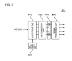
- FIG. 3 is a diagram illustrating a functional configuration of the reception device 40 .
- the reception device 40 includes a light front end 410 , a light source 420 , an AD conversion unit 430 , an adder unit 440 , and a signal processing unit 450 .
- the DA conversion unit 220 , the adder unit 440 , and the signal processing unit 450 are implemented as hardware by using, for example, integrated circuits.
- An optical signal received from the optical transmission path 60 and local light from the light source 420 are input to the light front end 410 .
- the light front end 410 causes the optical signal to interfere with the local light at a phase difference of 0 so as to generate a first optical signal (Ix), and causes the optical signal to interfere with the local light at a phase difference of ⁇ /2 so as to generate a second optical signal (Qx).
- the light front end 410 causes the optical signal to interfere with the local light at a phase difference of 0 so as to generate a third optical signal (Iy), and causes the optical signal to interfere with the local light at a phase difference of ⁇ /2 so as to generate a fourth optical signal (Qy).
- the first optical signal and the second optical signal form a set of signals
- the third optical signal and the fourth optical signal form a set of signals.
- the light front end 410 includes a photoelectric conversion element.
- the photoelectric conversion element is provided for each of the first to fourth optical signals, and converts each of the first to fourth optical signals into an electrical signal.
- the four electrical signals are based on orthogonal polarization and orthogonal phases.
- the light front end 410 has a filter characteristic. Assuming that the filter characteristic is, for example, a matching filter h*( ⁇ t), an electrical signal r(t) having undergone a process in the matching filter (electrical signal having undergone filter equalization) is given by the following Equation (2). Note that, in a case where a matching filter cannot be realized by the light front end 401 , a matching filter may be mounted in the signal processing unit 450 in a later stage.
- n(t) indicates white noise.
- the AD conversion unit 430 converts the four analog electrical signals generated by the light front end 410 into digital signals (quantization). Specifically, the AD conversion unit 430 samples the signals in a cycle T so as to quantize the signals.
- g m g(mT)
- ⁇ [m] ⁇ (mT)
- the first term of the right side indicates a target symbol
- the second term indicates inter-symbol interference
- the third term indicates a noise component
- the signal processing unit 450 processes the first signal (Ex) and the second signal (Ey) generated by the adder unit 440 so as to demodulate the four signals which have been transmitted.
- FIG. 4 is a diagram illustrating a functional configuration of the signal processing unit 450 (compensation unit).
- the signal processing unit 450 includes a frequency domain equalization unit 452 , a time domain equalization unit 454 , and a carrier reproduction unit 456 .
- the frequency domain equalization unit 452 performs an equalization process on each of the first signal and the second signal in a frequency domain. Details of the frequency domain equalization unit 452 will be described later with reference to FIG. 5 .
- the time domain equalization unit 454 performs an equalization process on each of the first signal and the second signal in a time domain so as to perform polarization separation.
- the time domain equalization unit 454 has, for example, an FIR filter.
- a filter coefficient applied to the FIR filter is controlled by, for example, an adaptive equalization algorithm such as a constant modulus algorithm (CMA).
- CMA constant modulus algorithm
- the carrier reproduction unit 456 compensates for (cancels) a frequency difference and a phase difference between an optical signal received from the optical transmission path 60 and light (local light) generated from the light source 420 according to, for example, an Mth Power algorithm, and then demodulates the four transmitted signals.
- FIG. 5 is a diagram illustrating details of the frequency domain equalization unit 452 .
- the frequency domain equalization unit 452 includes a Fourier transform unit 504 , a multiplication unit 506 (equalization processing unit), an inverse Fourier transform unit 508 , and an equalization coefficient setting unit 520 .
- the Fourier transform unit 504 performs a Fourier transform process on a signal (the first signal or the second signal) transmitted from the adder unit 440 , and obtains a resultant signal as information on a frequency axis. Note that, when being input to the Fourier transform unit 504 , the first signal and the second signal have been divided into signals in the predetermined time unit.
- the Fourier transform unit 504 performs the Fourier transform process on each of the separate signals (block signals which will be described later).
- the Fourier transform unit 504 divides the block signals converted on the frequency axis into signals in a unit of the predetermined frequency, and outputs the signals.
- the multiplication unit 506 multiplies each of the signals divided in the frequency unit by an equalization coefficient so as to perform an equalization process. Note that the equalization coefficient is individually set for each separate signal.
- the inverse Fourier transform unit 508 combines the separate signals having undergone the equalization process, and returns combined signals to information on a time axis by performing inverse Fourier transform on the combined signals, so as to generate block signals having undergone the equalization process.
- An equalization coefficient in this equalization process is set according to a method which will be described later. Therefore, through the equalization process, inter-symbol interference can be removed from a received signal, and a wavelength dispersion effect can be compensated for.
- the equalization coefficient setting unit 520 sets an equalization coefficient used in the multiplication unit 506 .
- the multiplication unit 506 includes a transfer function calculation unit 522 , a transfer function calculation unit 524 , a transfer function combination unit 526 , and an equalization coefficient calculation unit 528 .
- the transfer function calculation unit 522 calculates a diagonal matrix G(f) on the basis of a band limit condition g(t) used in the transmission device 20 and the reception device 40 .
- the transfer function calculation unit 524 calculates a diagonal matrix C(f) on the basis of a wavelength dispersion amount c(t) received from the optical transmission path.
- the equalization coefficient calculation unit 528 calculates an equalization coefficient matrix W(f) used in the multiplication unit 506 by using the diagonal matrix H(f).
- H H is a Hermitian transposed matrix of a matrix H
- E s is power of an optical signal
- ⁇ ⁇ is a diagonal matrix with N rows and N columns regarding noise.
- a diagonal component of ⁇ ⁇ is defined on the basis of colored noise included in an optical signal.
- MMSE minimum mean square error
- I indicates a unit matrix
- No indicates power of noise
- D is a discrete Fourier transform matrix with N rows and N columns
- ⁇ H is a Hermitian transposed (DFT) matrix of ⁇
- D H is an inverse DFT matrix.
- E[ ⁇ ] indicates an expected value.
- W colored (f) based on Equation (9) includes components other than a zero component in addition to a diagonal component, and thus a computation amount is increased if the above Equation (9) is used.
- DE[ ⁇ H ]D H in the above Equation (9) is approximated to a diagonal matrix.
- the above Equation (6) is derived.
- the equalization coefficient setting unit 520 may not include the transfer function calculation units 522 and 524 and the transfer function combination unit 526 .
- the diagonal matrix H(f) is input to the equalization coefficient calculation unit 528 from the outside of the equalization coefficient setting unit 520 .
- the equalization coefficient setting unit 520 may not include the transfer function calculation units 522 and 524 .
- the diagonal matrices G(f) and C(f) are input to the transfer function combination unit 526 from the outside of the equalization coefficient setting unit 520 .
- the frequency domain equalization unit 452 includes an overlap applying unit 502 , an overlap removal unit 510 , and an overlap control unit 512 .
- the overlap applying unit 502 is provided prior to the Fourier transform unit 504 , and divides an electrical signal to generate signals (hereinafter, referred to as block signals) in a unit of the process in the Fourier transform unit 504 .
- the overlap applying unit 502 causes adjacent block signals to overlap each other.
- the overlap control unit 512 controls an overlap amount applied by the overlap applying unit 502 .
- FIG. 6 is a diagram for explaining block signals generated by the overlap control unit 512 .
- the overlap control unit 512 divides an electrical signal into signals at the same interval (width M in FIG. 6 ).
- the overlap control unit 512 adds an overlap part with a predetermined width (p samples in FIG. 6 ) to each of all separate signals. This overlap part is the same content as the p samples that are from a tail of the previous signal.
- the overlap control unit 512 adds an overlap part with a predetermined width (q samples in FIG. 6 ) to a tail of each of all separate signals.
- the overlap part is the same content as the q samples that are from the tail of the next signal.
- the overlap control unit 512 generates each block signal. Note that the number of samples p and q may be equal to each other or may be different from each other.
- the number of samples p and q (that is, an overlap amount) of overlap is specified by the overlap control unit 512 as described above.
- inter-symbol interference of an electrical signal concentrates in the head and the tail of the block signal in the time axis.
- the overlap control unit 512 appropriately sets the number of samples p and q of overlap
- the inter-symbol interference of an electrical signal is removed due to removal of the overlap part in the overlap removal unit 510 .
- the overlap control unit 512 sets an overlap amount by using the above-described band limit condition g(t).
- the overlap control unit 512 increases the number of samples p and q of overlap.
- the overlap control unit 512 reduces the number of samples p and q of overlap.
- the overlap control unit 512 preferably sets an overlap amount not only by using the band limit condition g(t) but also by using the amount of wavelength dispersion c(t) which the optical signal incurred in the optical transmission path. Specifically, the overlap control unit 512 increases an overlap amount caused by a wavelength dispersion amount in a case where the wavelength dispersion amount is large. The overlap control unit 512 reduces an overlap amount caused by a wavelength dispersion amount in a case where the wavelength dispersion amount is small. The overlap control unit 512 adds the overlap amount based on the band limit to the overlap amount based on the wavelength dispersion amount so as to calculate the number of samples p and q of overlap used in the overlap applying unit 502 and the overlap removal unit 510 .
- the overlap removal unit 510 removes the overlap parts from the electrical signal (that is, the block signals) returned to information on the time axis by the inverse Fourier transform unit 508 .
- the overlap removal unit 510 receives the widths p and q of the signals to be removed at this time from the overlap control unit 512 .
- the signal processing unit 450 of the reception device 40 includes the frequency domain equalization unit 452 .
- the frequency domain equalization unit 452 performs an equalization process on a signal received in the frequency domain.
- An equalization coefficient in this case is set on the basis of the above Equation (6).
- ⁇ ⁇ included in the above Equation (6) is set by taking into consideration that noise included in a signal received by the reception device 40 is colored noise, and becomes a diagonal matrix through approximation. Therefore, a computation amount in the signal processing unit 450 is equal to a computation amount which is necessary in a case where noise included in a signal received by the reception device 40 is white noise, and equalization performance is improved compared with a case of using an MMSE coefficient of the related art.
- a communication system 10 according to the present example embodiment has the same configuration as that of the communication system 10 according to the first example embodiment except for a configuration of the frequency domain equalization unit 452 of the reception device 40 .
- FIG. 7 is a block diagram illustrating a configuration of the frequency domain equalization unit 452 according to the present example embodiment.
- the frequency domain equalization unit 452 according to the present example embodiment has the same configuration as that of the frequency domain equalization unit 452 according to the first example embodiment except that an equalization coefficient calculation unit 530 , an equalization coefficient calculation unit 532 , and an equalization coefficient combination unit 534 are provided instead of the transfer function combination unit 526 and the equalization coefficient calculation unit 528 .
- the equalization coefficient calculation unit 530 calculates an equalization coefficient matrix W 1 (f) by using a diagonal matrix C(f) which is calculated on the basis of a wavelength dispersion amount by the transfer function calculation unit 524 .
- the equalization coefficient calculation unit 532 calculates an equalization coefficient matrix W 2 (f) by using a diagonal matrix G(f) which is calculated on the basis of band limit information by the transfer function calculation unit 522 .
- the equalization coefficient matrix W 2 (f) is calculated according to the following Equation (11).
- W 2 ( f ) G H ( G ( f ) H G ( f )+(1/ E s ) ⁇ ⁇ ) ⁇ 1 (11)
- G(f) H is a Hermitian transposed matrix of a matrix G(f).
- E s are ⁇ ⁇ are the same as those described in the first example embodiment.
- a computation amount in the signal processing unit 450 is equal to a computation amount which is necessary in a case where noise included in a signal received by the reception device 40 is white noise, and equalization performance is improved compared with a case of using an MMSE coefficient of the related art.
- a communication system 10 according to the present example embodiment has the same configuration as that of the communication system 10 according to the first example embodiment or the second example embodiment except for a configuration of the signal processing unit 450 .
- FIG. 8 is a diagram illustrating a configuration of the signal processing unit 450 according to the present example embodiment.
- the signal processing unit 450 illustrated in FIG. 8 has the same configuration as that of the signal processing unit 450 according to the first example embodiment or the second example embodiment except that a maximum likelihood sequence estimation unit 458 is provided.
- the maximum likelihood sequence estimation unit 458 performs a process (that is, a maximum likelihood sequence estimation process) based on a maximum likelihood sequence estimation (MLSE) algorithm on each of four signals demodulated by the carrier reproduction unit 456 . Consequently, inter-symbol interference is further removed from each of the four signals.
- the maximum likelihood sequence estimation unit 458 is implemented by, for example, a circuit.
- a computation amount in the signal processing unit 450 is equal to a computation amount which is necessary in a case where noise included in a signal received by the reception device 40 is white noise, and equalization performance is improved compared with a case of using an MMSE coefficient of the related art.
- the four signals demodulated by the carrier reproduction unit 456 are processed by the maximum likelihood sequence estimation unit 458 , and thus inter-symbol interference is further removed from each of the four signals.
- a signal processing device including:
- an electrical signal generation unit generating an electrical signal on the basis of an optical signal which is polarization-multiplexed and multi-value-modulated and which is transmitted through an optical transmission path;
- a compensation unit performing a compensation process on the electrical signal
- the compensation unit includes:
- equalization coefficient setting unit sets the equalization coefficient matrix W(f) on the basis of the following equation.
- W ( f ) H ( f ) H ( H ( f ) H H ( f )+(1/ E s ) ⁇ ⁇ ) ⁇ 1
- H(f) G(f) ⁇ C(f)
- H H is a Hermitian transposed matrix of a matrix H
- E s is power of the optical signal
- ⁇ ⁇ is a diagonal matrix with N rows and N columns defined on the basis of colored noise.
- G(f) is a diagonal matrix set on the basis of a band limit condition during generation of the optical signal
- C(f) is a diagonal matrix set on the basis of wavelength dispersion incurred in the optical transmission path.
- a signal processing device including:
- an electrical signal generation unit generating an electrical signal on the basis of an optical signal which is polarization-multiplexed and multi-value-modulated and which is transmitted through an optical transmission path;
- a compensation unit performing a compensation process on the electrical signal
- the compensation unit includes:
- equalization coefficient setting unit sets the equalization coefficient matrix W(f) on the basis of the following equation.
- W ( f ) W 1 ( f ) ⁇ W 2 ( f )
- G(f) H is a Hermitian transposed matrix of a matrix G(f)
- E s is power of the electrical signal
- ⁇ ⁇ is a diagonal matrix with N rows and N columns defined on the basis of colored noise.
- G(f) is a diagonal matrix set on the basis of a band limit condition during generation of the optical signal
- C(f) is a diagonal matrix set on the basis of a wavelength dispersion condition incurred in the optical transmission path.
- compensation unit further includes:
- the signal processing device further including an overlap control unit setting a magnitude of the overlap, on the basis of the band limit condition and a compensation amount for compensating for the wavelength dispersion.
- optical signal is transmitted according to wavelength division multiplexing communication (WDM)
- WDM wavelength division multiplexing communication
- a single band in wavelength division multiplexing communication is set to be narrower than in a Nyquist condition.
- a communication system including:
- a signal transmission device generating and transmitting an optical signal
- a signal processing device receiving and processing the optical signal
- the signal transmission device generates the optical signal through polarization multiplexing and multi-value modulation
- the signal processing device is the signal processing device according to appendix 1 or 2.
- compensation unit further includes:
- optical signal is transmitted according to wavelength division multiplexing communication (WDM)
- WDM wavelength division multiplexing communication
- a single band in wavelength division multiplexing communication is set to be narrower than in a Nyquist condition.
- a signal processing method of receiving and processing an optical signal including:
- compensation unit further includes:
- the signal processing method according to appendix 16 or 17, further including an overlap control unit setting a magnitude of the overlap, on the basis of the band limit condition and a compensation amount for compensating for the wavelength dispersion.
- optical signal is transmitted according to wavelength division multiplexing communication (WDM)
- WDM wavelength division multiplexing communication
- a single band in wavelength division multiplexing communication is set to be narrower than in a Nyquist condition.
Landscapes
- Engineering & Computer Science (AREA)
- Computer Networks & Wireless Communication (AREA)
- Signal Processing (AREA)
- Physics & Mathematics (AREA)
- Electromagnetism (AREA)
- Nonlinear Science (AREA)
- Optical Communication System (AREA)
- Cable Transmission Systems, Equalization Of Radio And Reduction Of Echo (AREA)
Abstract
Description
-
- a Fourier transform unit performing Fourier transform on the electrical signal;
- an equalization processing unit performing an equalization process on the electrical signal having undergone the Fourier transform in a frequency domain;
- an inverse Fourier transform unit performing inverse Fourier transform on the electrical signal having undergone the equalization process; and
- an equalization coefficient setting unit setting an equalization coefficient matrix W(f) used for the equalization process, and
W(f)=H(f)H(H(f)H H(f)+(1/E s)×Φη)−1
-
- a Fourier transform unit performing Fourier transform on the electrical signal;
- an equalization processing unit performing an equalization process on the electrical signal having undergone the Fourier transform in a frequency domain;
- an inverse Fourier transform unit performing inverse Fourier transform on the electrical signal having undergone the equalization process; and
- an equalization coefficient setting unit setting an equalization coefficient matrix W(f) used for the equalization process, and
W(f)=W 1(f)×W 2(f)
g(t)=∫−∞ ∞ h(τ)h*(τ−t)dτ (3)
η(t)=∫−∞ ∞ n(τ)h*(τ−t)dτ (4)
W(f)=H(f)H(H(f)H H(f)+(1/E s)×Φη)−1 (6)
W 1(f)=C(f)−1 (10)
W 2(f)=G H(G(f)H G(f)+(1/E s)×Φη)−1 (11)
-
- a Fourier transform unit performing Fourier transform on the electrical signal;
- an equalization processing unit performing an equalization process on the electrical signal having undergone the Fourier transform in a frequency domain;
- an inverse Fourier transform unit performing inverse Fourier transform on the electrical signal having undergone the equalization process; and
- an equalization coefficient setting unit setting an equalization coefficient matrix W(f) used for the equalization process, and
W(f)=H(f)H(H(f)H H(f)+(1/E s)×Φη)−1
-
- a Fourier transform unit performing Fourier transform on the electrical signal;
- an equalization processing unit performing an equalization process on the electrical signal having undergone the Fourier transform in a frequency domain;
- an inverse Fourier transform unit performing inverse Fourier transform on the electrical signal having undergone the equalization process; and
- an equalization coefficient setting unit setting an equalization coefficient matrix W(f) used for the equalization process, and
W(f)=W 1(f)×W 2(f)
-
- an overlap applying unit dividing the electrical signal so as to generate block signals which are signals in a unit of a process in the Fourier transform unit such that overlap occurs in the block signals adjacent to each other; and
- an overlap removal unit removing the overlap from the block signals having undergone inverse Fourier transform in the inverse Fourier transform unit, and connects the block signals after the removal to each other.
-
- an overlap applying unit dividing the electrical signal so as to generate block signals which are signals in a unit of process in the Fourier transform unit such that overlap occurs in the block signals adjacent to each other, and
- an overlap removal unit removing the overlap from the block signals having undergone inverse Fourier transform in the inverse Fourier transform unit, and connecting the block signals after the removal to each other.
Claims (9)
W(f)=H(f)H(f)(H(f)H H(f)+(1/Es)×Φη −1
W(f)=W 1(f)×W 2(f)
Applications Claiming Priority (3)
| Application Number | Priority Date | Filing Date | Title |
|---|---|---|---|
| JP2015-163904 | 2015-08-21 | ||
| JP2015163904 | 2015-08-21 | ||
| PCT/JP2016/068464 WO2017033550A1 (en) | 2015-08-21 | 2016-06-22 | Signal processing device, communication system, and signal processing method |
Publications (2)
| Publication Number | Publication Date |
|---|---|
| US20180248582A1 US20180248582A1 (en) | 2018-08-30 |
| US10193593B2 true US10193593B2 (en) | 2019-01-29 |
Family
ID=58099883
Family Applications (1)
| Application Number | Title | Priority Date | Filing Date |
|---|---|---|---|
| US15/753,694 Active US10193593B2 (en) | 2015-08-21 | 2016-06-22 | Signal processing device, communication system, and signal processing method |
Country Status (3)
| Country | Link |
|---|---|
| US (1) | US10193593B2 (en) |
| JP (1) | JP6711358B2 (en) |
| WO (1) | WO2017033550A1 (en) |
Cited By (3)
| Publication number | Priority date | Publication date | Assignee | Title |
|---|---|---|---|---|
| US11316588B2 (en) * | 2018-09-26 | 2022-04-26 | Nippon Telegraph And Telephone Corporation | Wavelength dispersion compensation apparatus, wavelength dispersion compensation method, and optical receiving apparatus |
| US11381317B2 (en) * | 2019-01-09 | 2022-07-05 | Nippon Telegraph And Telephone Corporation | Optical receiving apparatus and waveform distortion compensation method |
| EP4120593A4 (en) * | 2020-03-11 | 2024-01-03 | Nippon Telegraph And Telephone Corporation | OPTICAL RECEIVING DEVICE AND OPTICAL RECEIVING METHOD |
Families Citing this family (11)
| Publication number | Priority date | Publication date | Assignee | Title |
|---|---|---|---|---|
| JP7213987B2 (en) * | 2018-09-11 | 2023-01-27 | ホアウェイ・テクノロジーズ・カンパニー・リミテッド | Equalizer for compensating for abrupt changes in the polarization state of an optical signal |
| EP3965319B1 (en) * | 2019-06-06 | 2024-08-07 | Nippon Telegraph And Telephone Corporation | Wavelength dispersion compensation device, light reception device, wavelength dispersion compensation method, and computer program |
| EP3987690A1 (en) | 2019-06-21 | 2022-04-27 | Fraunhofer-Gesellschaft zur Förderung der angewandten Forschung e.V. | Apparatus and method for transmitting and/or receiving data over a fiber-optical channel employing perturbation-based fiber nonlinearity compensation in a periodic frequency domain |
| JPWO2022003920A1 (en) * | 2020-07-02 | 2022-01-06 | ||
| EP4335050A4 (en) * | 2021-05-31 | 2024-07-24 | Huawei Technologies Canada Co., Ltd. | Methods and systems for a 2-qubit multi-user quantum key distribution protocol |
| CA3226705A1 (en) * | 2021-07-20 | 2023-01-26 | The Research Foundation For The State University Of New York | System and method for quantum-secure microgrids |
| US12250101B1 (en) * | 2022-01-18 | 2025-03-11 | Cisco Technology, Inc. | Coherent optical module for short reach communications |
| CN120226285A (en) * | 2022-11-25 | 2025-06-27 | 日本电信电话株式会社 | Wavelength dispersion compensation device and coefficient optimization method |
| JP2024118747A (en) * | 2023-02-21 | 2024-09-02 | 日本電気株式会社 | Receiver, shared information generation method, communication control method, and program in continuous quantum key distribution system |
| JP7753277B2 (en) * | 2023-03-17 | 2025-10-14 | 株式会社東芝 | Key management device, quantum cryptography communication system, QKDN control device, information processing device, key management method, QKDN control method, information processing method, and program |
| US20250106012A1 (en) * | 2023-09-26 | 2025-03-27 | Ciena Corporation | Quantum key distribution in an optical network and quantum-secured optical channels |
Citations (9)
| Publication number | Priority date | Publication date | Assignee | Title |
|---|---|---|---|---|
| JP2011004264A (en) | 2009-06-19 | 2011-01-06 | Fujitsu Ltd | Digital signal processing apparatus and method |
| US20110129041A1 (en) * | 2008-06-20 | 2011-06-02 | Nippon Telegraph And Telephone Corporation | Receiver device, communication system and receiving method |
| US20120127923A1 (en) | 2010-11-23 | 2012-05-24 | Wanlun Zhao | Method and Apparatus for Enabling a Low Complexity Receiver |
| JP2012528523A (en) | 2009-05-29 | 2012-11-12 | トムソン ライセンシング | Method and apparatus for repetitive timing reproduction |
| US20130195459A1 (en) * | 2010-03-19 | 2013-08-01 | Ofidium Pty Ltd. | Method and apparatus for fiber non-linearity mitigation |
| US20130272719A1 (en) * | 2012-04-11 | 2013-10-17 | Fujitsu Limited | Method and Apparatus for Compensating Nonlinear Distortions in Intensity Modulation-Direct Detection System |
| WO2015075895A1 (en) | 2013-11-19 | 2015-05-28 | 日本電気株式会社 | Nonlinear distortion compensator, light receiver using same, and nonlinear distortion compensation method |
| US20160241341A1 (en) * | 2015-02-18 | 2016-08-18 | Fujitsu Limited | Optical transmission apparatus, optical transmission system, and polarization dependent loss monitor |
| US20170180055A1 (en) * | 2015-12-21 | 2017-06-22 | Zte Corporation | Techniques for receiving dft spreading modulation signals |
-
2016
- 2016-06-22 JP JP2017536649A patent/JP6711358B2/en active Active
- 2016-06-22 US US15/753,694 patent/US10193593B2/en active Active
- 2016-06-22 WO PCT/JP2016/068464 patent/WO2017033550A1/en not_active Ceased
Patent Citations (10)
| Publication number | Priority date | Publication date | Assignee | Title |
|---|---|---|---|---|
| US20110129041A1 (en) * | 2008-06-20 | 2011-06-02 | Nippon Telegraph And Telephone Corporation | Receiver device, communication system and receiving method |
| JP2012528523A (en) | 2009-05-29 | 2012-11-12 | トムソン ライセンシング | Method and apparatus for repetitive timing reproduction |
| JP2011004264A (en) | 2009-06-19 | 2011-01-06 | Fujitsu Ltd | Digital signal processing apparatus and method |
| US20130195459A1 (en) * | 2010-03-19 | 2013-08-01 | Ofidium Pty Ltd. | Method and apparatus for fiber non-linearity mitigation |
| US20120127923A1 (en) | 2010-11-23 | 2012-05-24 | Wanlun Zhao | Method and Apparatus for Enabling a Low Complexity Receiver |
| WO2012071558A1 (en) | 2010-11-23 | 2012-05-31 | Qualcomm Incorporated | Method and apparatus for enabling a low complexity receiver |
| US20130272719A1 (en) * | 2012-04-11 | 2013-10-17 | Fujitsu Limited | Method and Apparatus for Compensating Nonlinear Distortions in Intensity Modulation-Direct Detection System |
| WO2015075895A1 (en) | 2013-11-19 | 2015-05-28 | 日本電気株式会社 | Nonlinear distortion compensator, light receiver using same, and nonlinear distortion compensation method |
| US20160241341A1 (en) * | 2015-02-18 | 2016-08-18 | Fujitsu Limited | Optical transmission apparatus, optical transmission system, and polarization dependent loss monitor |
| US20170180055A1 (en) * | 2015-12-21 | 2017-06-22 | Zte Corporation | Techniques for receiving dft spreading modulation signals |
Non-Patent Citations (1)
| Title |
|---|
| International Search Report for PCT/JP2016/068464 dated Aug. 23, 2016 [PCT/ISA/210]. |
Cited By (3)
| Publication number | Priority date | Publication date | Assignee | Title |
|---|---|---|---|---|
| US11316588B2 (en) * | 2018-09-26 | 2022-04-26 | Nippon Telegraph And Telephone Corporation | Wavelength dispersion compensation apparatus, wavelength dispersion compensation method, and optical receiving apparatus |
| US11381317B2 (en) * | 2019-01-09 | 2022-07-05 | Nippon Telegraph And Telephone Corporation | Optical receiving apparatus and waveform distortion compensation method |
| EP4120593A4 (en) * | 2020-03-11 | 2024-01-03 | Nippon Telegraph And Telephone Corporation | OPTICAL RECEIVING DEVICE AND OPTICAL RECEIVING METHOD |
Also Published As
| Publication number | Publication date |
|---|---|
| JPWO2017033550A1 (en) | 2018-07-12 |
| WO2017033550A1 (en) | 2017-03-02 |
| US20180248582A1 (en) | 2018-08-30 |
| JP6711358B2 (en) | 2020-06-17 |
Similar Documents
| Publication | Publication Date | Title |
|---|---|---|
| US10193593B2 (en) | Signal processing device, communication system, and signal processing method | |
| US9853765B2 (en) | Signal processing device and signal processing method for optical polarization multiplexed signal | |
| EP3553973B1 (en) | Optical transmission characteristic estimation method, optical transmission characteristic compensation method, optical transmission characteristic estimation system and optical transmission characteristic compensation system | |
| US8472813B2 (en) | Computationally-efficient MIMO equalization algorithm for high-speed, real-time, adaptive polarization multiplexed (POLMUX) OFDM transmission with direct detection | |
| JP6485670B2 (en) | Method for decoding optical signal and receiver for receiving and decoding optical signal | |
| JP5842472B2 (en) | Self-phase modulation noise calculation device, self-phase modulation noise elimination device, and optical coherent receiver | |
| US20160050025A1 (en) | Signal processing device, optical communication system, and signal processing method | |
| US8718474B2 (en) | Chromatic dispersion compensation using sign operations and lookup tables | |
| JPWO2018079598A1 (en) | Optical receiver, optical receiving method, and optical communication system | |
| JP2019041285A (en) | Optical transmission characteristic compensation system and optical transmission characteristic compensation method | |
| WO2019043747A1 (en) | Optical communication device | |
| US8989324B2 (en) | Receiver and receiving method | |
| US8682174B2 (en) | Optical receiver, optical communication system using the same and equalization method in the optical communication system | |
| US11502754B2 (en) | Equalizing device for compensating rapid state of polarization changes of an optical signal | |
| US11632184B2 (en) | Wavelength-division multiplexing optical transmission system, wavelength-division multiplexing optical transmission method, and non-transitory computer readable medium | |
| JP6355465B2 (en) | Optical receiver, transmitter / receiver, optical communication system, and waveform distortion compensation method | |
| JP5681743B2 (en) | Optical receiving apparatus and optical receiving method | |
| EP3133751A1 (en) | Method for nonlinearity compensation in optical transmission systems | |
| US11581951B1 (en) | Apparatuses and methods of far-end transmitter skew monitoring in digital subcarrier multiplexing systems | |
| WO2012051668A1 (en) | Bispectrum method and apparatus for recovery of optically transmitted signals | |
| KR20030063114A (en) | Ghost Eliminating Equalizer |
Legal Events
| Date | Code | Title | Description |
|---|---|---|---|
| AS | Assignment |
Owner name: NEC CORPORATION, JAPAN Free format text: ASSIGNMENT OF ASSIGNORS INTEREST;ASSIGNORS:YASUDA, WAKAKO;HAYASHI, KAZUNORI;REEL/FRAME:044976/0732 Effective date: 20180130 |
|
| FEPP | Fee payment procedure |
Free format text: ENTITY STATUS SET TO UNDISCOUNTED (ORIGINAL EVENT CODE: BIG.); ENTITY STATUS OF PATENT OWNER: LARGE ENTITY |
|
| STCF | Information on status: patent grant |
Free format text: PATENTED CASE |
|
| CC | Certificate of correction | ||
| MAFP | Maintenance fee payment |
Free format text: PAYMENT OF MAINTENANCE FEE, 4TH YEAR, LARGE ENTITY (ORIGINAL EVENT CODE: M1551); ENTITY STATUS OF PATENT OWNER: LARGE ENTITY Year of fee payment: 4 |