US10192917B2 - Backside illuminated photosensor element with light pipe and light mirror structures - Google Patents
Backside illuminated photosensor element with light pipe and light mirror structures Download PDFInfo
- Publication number
- US10192917B2 US10192917B2 US15/198,824 US201615198824A US10192917B2 US 10192917 B2 US10192917 B2 US 10192917B2 US 201615198824 A US201615198824 A US 201615198824A US 10192917 B2 US10192917 B2 US 10192917B2
- Authority
- US
- United States
- Prior art keywords
- layer
- photosensor
- semiconductor substrate
- active region
- region
- Prior art date
- Legal status (The legal status is an assumption and is not a legal conclusion. Google has not performed a legal analysis and makes no representation as to the accuracy of the status listed.)
- Active, expires
Links
- 239000000758 substrate Substances 0.000 claims abstract description 116
- 239000004065 semiconductor Substances 0.000 claims abstract description 68
- 210000001747 pupil Anatomy 0.000 claims abstract description 27
- 238000002955 isolation Methods 0.000 claims abstract description 22
- 239000010410 layer Substances 0.000 claims description 92
- 239000000463 material Substances 0.000 claims description 17
- 239000012780 transparent material Substances 0.000 claims description 14
- 239000007769 metal material Substances 0.000 claims description 13
- 239000006117 anti-reflective coating Substances 0.000 claims description 9
- WFKWXMTUELFFGS-UHFFFAOYSA-N tungsten Chemical compound [W] WFKWXMTUELFFGS-UHFFFAOYSA-N 0.000 claims description 6
- 229910052721 tungsten Inorganic materials 0.000 claims description 6
- 239000010937 tungsten Substances 0.000 claims description 6
- VYZAMTAEIAYCRO-UHFFFAOYSA-N Chromium Chemical compound [Cr] VYZAMTAEIAYCRO-UHFFFAOYSA-N 0.000 claims description 5
- RYGMFSIKBFXOCR-UHFFFAOYSA-N Copper Chemical compound [Cu] RYGMFSIKBFXOCR-UHFFFAOYSA-N 0.000 claims description 5
- 229910001069 Ti alloy Inorganic materials 0.000 claims description 5
- RTAQQCXQSZGOHL-UHFFFAOYSA-N Titanium Chemical compound [Ti] RTAQQCXQSZGOHL-UHFFFAOYSA-N 0.000 claims description 5
- NRTOMJZYCJJWKI-UHFFFAOYSA-N Titanium nitride Chemical compound [Ti]#N NRTOMJZYCJJWKI-UHFFFAOYSA-N 0.000 claims description 5
- 229910052782 aluminium Inorganic materials 0.000 claims description 5
- XAGFODPZIPBFFR-UHFFFAOYSA-N aluminium Chemical compound [Al] XAGFODPZIPBFFR-UHFFFAOYSA-N 0.000 claims description 5
- 229910052804 chromium Inorganic materials 0.000 claims description 5
- 239000011651 chromium Substances 0.000 claims description 5
- 229910052802 copper Inorganic materials 0.000 claims description 5
- 239000010949 copper Substances 0.000 claims description 5
- 239000010936 titanium Substances 0.000 claims description 5
- 229910052719 titanium Inorganic materials 0.000 claims description 5
- 230000035945 sensitivity Effects 0.000 description 12
- 239000002019 doping agent Substances 0.000 description 10
- 229910052751 metal Inorganic materials 0.000 description 10
- 239000002184 metal Substances 0.000 description 10
- 210000000746 body region Anatomy 0.000 description 6
- XUIMIQQOPSSXEZ-UHFFFAOYSA-N Silicon Chemical compound [Si] XUIMIQQOPSSXEZ-UHFFFAOYSA-N 0.000 description 5
- 230000003287 optical effect Effects 0.000 description 5
- 229910052710 silicon Inorganic materials 0.000 description 5
- 239000010703 silicon Substances 0.000 description 5
- IJGRMHOSHXDMSA-UHFFFAOYSA-N Atomic nitrogen Chemical compound N#N IJGRMHOSHXDMSA-UHFFFAOYSA-N 0.000 description 4
- 230000002093 peripheral effect Effects 0.000 description 4
- 229910052581 Si3N4 Inorganic materials 0.000 description 3
- HQVNEWCFYHHQES-UHFFFAOYSA-N silicon nitride Chemical compound N12[Si]34N5[Si]62N3[Si]51N64 HQVNEWCFYHHQES-UHFFFAOYSA-N 0.000 description 3
- QVGXLLKOCUKJST-UHFFFAOYSA-N atomic oxygen Chemical compound [O] QVGXLLKOCUKJST-UHFFFAOYSA-N 0.000 description 2
- 238000001465 metallisation Methods 0.000 description 2
- 238000012986 modification Methods 0.000 description 2
- 230000004048 modification Effects 0.000 description 2
- 229910052757 nitrogen Inorganic materials 0.000 description 2
- 239000001301 oxygen Substances 0.000 description 2
- 229910052760 oxygen Inorganic materials 0.000 description 2
- LIVNPJMFVYWSIS-UHFFFAOYSA-N silicon monoxide Chemical compound [Si-]#[O+] LIVNPJMFVYWSIS-UHFFFAOYSA-N 0.000 description 2
- VYPSYNLAJGMNEJ-UHFFFAOYSA-N Silicium dioxide Chemical compound O=[Si]=O VYPSYNLAJGMNEJ-UHFFFAOYSA-N 0.000 description 1
- 230000006978 adaptation Effects 0.000 description 1
- 239000000969 carrier Substances 0.000 description 1
- 239000011248 coating agent Substances 0.000 description 1
- 238000000576 coating method Methods 0.000 description 1
- 230000005684 electric field Effects 0.000 description 1
- 239000003574 free electron Substances 0.000 description 1
- 238000003384 imaging method Methods 0.000 description 1
- 239000012212 insulator Substances 0.000 description 1
- 229910044991 metal oxide Inorganic materials 0.000 description 1
- 150000004706 metal oxides Chemical class 0.000 description 1
- 238000000034 method Methods 0.000 description 1
- 229920000620 organic polymer Polymers 0.000 description 1
- 239000011347 resin Substances 0.000 description 1
- 229920005989 resin Polymers 0.000 description 1
- 229910052814 silicon oxide Inorganic materials 0.000 description 1
Images


Classifications
-
- H—ELECTRICITY
- H01—ELECTRIC ELEMENTS
- H01L—SEMICONDUCTOR DEVICES NOT COVERED BY CLASS H10
- H01L27/00—Devices consisting of a plurality of semiconductor or other solid-state components formed in or on a common substrate
- H01L27/14—Devices consisting of a plurality of semiconductor or other solid-state components formed in or on a common substrate including semiconductor components sensitive to infrared radiation, light, electromagnetic radiation of shorter wavelength or corpuscular radiation and specially adapted either for the conversion of the energy of such radiation into electrical energy or for the control of electrical energy by such radiation
- H01L27/144—Devices controlled by radiation
- H01L27/146—Imager structures
- H01L27/14601—Structural or functional details thereof
- H01L27/14625—Optical elements or arrangements associated with the device
- H01L27/14629—Reflectors
-
- H—ELECTRICITY
- H01—ELECTRIC ELEMENTS
- H01L—SEMICONDUCTOR DEVICES NOT COVERED BY CLASS H10
- H01L27/00—Devices consisting of a plurality of semiconductor or other solid-state components formed in or on a common substrate
- H01L27/14—Devices consisting of a plurality of semiconductor or other solid-state components formed in or on a common substrate including semiconductor components sensitive to infrared radiation, light, electromagnetic radiation of shorter wavelength or corpuscular radiation and specially adapted either for the conversion of the energy of such radiation into electrical energy or for the control of electrical energy by such radiation
- H01L27/144—Devices controlled by radiation
- H01L27/146—Imager structures
- H01L27/14601—Structural or functional details thereof
- H01L27/14609—Pixel-elements with integrated switching, control, storage or amplification elements
- H01L27/14612—Pixel-elements with integrated switching, control, storage or amplification elements involving a transistor
-
- H—ELECTRICITY
- H01—ELECTRIC ELEMENTS
- H01L—SEMICONDUCTOR DEVICES NOT COVERED BY CLASS H10
- H01L27/00—Devices consisting of a plurality of semiconductor or other solid-state components formed in or on a common substrate
- H01L27/14—Devices consisting of a plurality of semiconductor or other solid-state components formed in or on a common substrate including semiconductor components sensitive to infrared radiation, light, electromagnetic radiation of shorter wavelength or corpuscular radiation and specially adapted either for the conversion of the energy of such radiation into electrical energy or for the control of electrical energy by such radiation
- H01L27/144—Devices controlled by radiation
- H01L27/146—Imager structures
- H01L27/14601—Structural or functional details thereof
- H01L27/1462—Coatings
-
- H—ELECTRICITY
- H01—ELECTRIC ELEMENTS
- H01L—SEMICONDUCTOR DEVICES NOT COVERED BY CLASS H10
- H01L27/00—Devices consisting of a plurality of semiconductor or other solid-state components formed in or on a common substrate
- H01L27/14—Devices consisting of a plurality of semiconductor or other solid-state components formed in or on a common substrate including semiconductor components sensitive to infrared radiation, light, electromagnetic radiation of shorter wavelength or corpuscular radiation and specially adapted either for the conversion of the energy of such radiation into electrical energy or for the control of electrical energy by such radiation
- H01L27/144—Devices controlled by radiation
- H01L27/146—Imager structures
- H01L27/14601—Structural or functional details thereof
- H01L27/14625—Optical elements or arrangements associated with the device
- H01L27/14627—Microlenses
-
- H—ELECTRICITY
- H01—ELECTRIC ELEMENTS
- H01L—SEMICONDUCTOR DEVICES NOT COVERED BY CLASS H10
- H01L27/00—Devices consisting of a plurality of semiconductor or other solid-state components formed in or on a common substrate
- H01L27/14—Devices consisting of a plurality of semiconductor or other solid-state components formed in or on a common substrate including semiconductor components sensitive to infrared radiation, light, electromagnetic radiation of shorter wavelength or corpuscular radiation and specially adapted either for the conversion of the energy of such radiation into electrical energy or for the control of electrical energy by such radiation
- H01L27/144—Devices controlled by radiation
- H01L27/146—Imager structures
- H01L27/14601—Structural or functional details thereof
- H01L27/1463—Pixel isolation structures
-
- H—ELECTRICITY
- H01—ELECTRIC ELEMENTS
- H01L—SEMICONDUCTOR DEVICES NOT COVERED BY CLASS H10
- H01L27/00—Devices consisting of a plurality of semiconductor or other solid-state components formed in or on a common substrate
- H01L27/14—Devices consisting of a plurality of semiconductor or other solid-state components formed in or on a common substrate including semiconductor components sensitive to infrared radiation, light, electromagnetic radiation of shorter wavelength or corpuscular radiation and specially adapted either for the conversion of the energy of such radiation into electrical energy or for the control of electrical energy by such radiation
- H01L27/144—Devices controlled by radiation
- H01L27/146—Imager structures
- H01L27/14601—Structural or functional details thereof
- H01L27/1464—Back illuminated imager structures
-
- H—ELECTRICITY
- H01—ELECTRIC ELEMENTS
- H01L—SEMICONDUCTOR DEVICES NOT COVERED BY CLASS H10
- H01L27/00—Devices consisting of a plurality of semiconductor or other solid-state components formed in or on a common substrate
- H01L27/14—Devices consisting of a plurality of semiconductor or other solid-state components formed in or on a common substrate including semiconductor components sensitive to infrared radiation, light, electromagnetic radiation of shorter wavelength or corpuscular radiation and specially adapted either for the conversion of the energy of such radiation into electrical energy or for the control of electrical energy by such radiation
- H01L27/144—Devices controlled by radiation
- H01L27/146—Imager structures
- H01L27/14601—Structural or functional details thereof
- H01L27/14609—Pixel-elements with integrated switching, control, storage or amplification elements
-
- H—ELECTRICITY
- H01—ELECTRIC ELEMENTS
- H01L—SEMICONDUCTOR DEVICES NOT COVERED BY CLASS H10
- H01L27/00—Devices consisting of a plurality of semiconductor or other solid-state components formed in or on a common substrate
- H01L27/14—Devices consisting of a plurality of semiconductor or other solid-state components formed in or on a common substrate including semiconductor components sensitive to infrared radiation, light, electromagnetic radiation of shorter wavelength or corpuscular radiation and specially adapted either for the conversion of the energy of such radiation into electrical energy or for the control of electrical energy by such radiation
- H01L27/144—Devices controlled by radiation
- H01L27/146—Imager structures
- H01L27/14601—Structural or functional details thereof
- H01L27/1462—Coatings
- H01L27/14623—Optical shielding
-
- H—ELECTRICITY
- H01—ELECTRIC ELEMENTS
- H01L—SEMICONDUCTOR DEVICES NOT COVERED BY CLASS H10
- H01L27/00—Devices consisting of a plurality of semiconductor or other solid-state components formed in or on a common substrate
- H01L27/14—Devices consisting of a plurality of semiconductor or other solid-state components formed in or on a common substrate including semiconductor components sensitive to infrared radiation, light, electromagnetic radiation of shorter wavelength or corpuscular radiation and specially adapted either for the conversion of the energy of such radiation into electrical energy or for the control of electrical energy by such radiation
- H01L27/144—Devices controlled by radiation
- H01L27/146—Imager structures
- H01L27/14601—Structural or functional details thereof
- H01L27/14625—Optical elements or arrangements associated with the device
Definitions
- the present invention relates to backside illuminated photosensor elements.
- FIG. 1 showing a cross-section of a conventional backside illuminated photosensor element 10 .
- the illustration in FIG. 1 is of just a single element (also referred to as a pixel), it being understood that an image sensor is formed of a plurality of such photosensor elements typically arranged in an array.
- the element 10 comprises a semiconductor substrate 12 that is doped with a first conductivity type dopant (for example, a p-type dopant) with a dopant concentration of 1 ⁇ 10 15 to 5 ⁇ 10 16 at/cm 3 .
- the semiconductor substrate 12 may, for example, be made of silicon and have a thickness of 3-10 ⁇ m.
- the semiconductor substrate 12 may comprise the upper silicon layer of a silicon-on-insulator (SOI) substrate that is produced in a process where a handle is attached to the front of the SOI substrate and the back of the SOI substrate is thinned to remove the carrier substrate and buried oxide layers.
- SOI silicon-on-insulator
- a region 16 is provided for trapping photogenerated carriers and charge transfer components.
- the region 16 is doped with a second conductivity type dopant (for example, an n-type dopant) with a dopant concentration of 1 ⁇ 10 17 to 1 ⁇ 10 19 at/cm 3 .
- a circuit 18 for transferring photogenerated charge is also provided at the front surface 14 .
- the circuit 18 comprises a metal oxide semiconductor (MOS) transistor including an insulated gate 20 and a read region 22 .
- the read region 22 is doped with the second conductivity type dopant with a dopant concentration of 1 ⁇ 10 19 to 1 ⁇ 10 21 at/cm 3 .
- MOS metal oxide semiconductor
- the insulated gate 20 extends over a channel portion of the substrate 12 between the regions 16 and 22 which form source-drain regions of the MOS transistor.
- the conductive tracks 32 of the interconnection circuits may be electrically coupled to the insulated gate 20 , read region 22 and substrate 12 body using contact structures (not shown) such as, for example, tungsten plugs.
- Each photosensor element includes a pixel substrate (active) region 40 formed by a portion of the substrate 12 that includes the regions 16 and 22 .
- the pixel substrate region 40 is delimited by a surrounding isolation structure 42 that extends from the front surface 14 to the back surface 44 of the semiconductor substrate 12 .
- the isolation structure 42 includes a core region 46 formed of a reflective metal material such as, for example, aluminum, titanium, titanium nitride, titanium alloy, tungsten, chromium, copper, and the like.
- the isolation structure 42 further includes a peripheral region 48 , lining the core region 46 and further a dielectric peripheral region 49 lining the region 48 and positioned between the core region 46 and the pixel substrate region 40 .
- the peripheral region 48 may, for example, be doped with the first conductivity type dopant with a dopant concentration of 1 ⁇ 10 18 to 1 ⁇ 10 20 at/cm 3 .
- the peripheral region 49 may comprise, for example, silicon oxide or silicon nitride material.
- a layer 50 made of an antireflection dielectric coating (ARC) material is mounted to the back surface 44 of the semiconductor substrate 12 .
- the ARC material may, for example, comprise a resin, an organic polymer, a material including silicon and nitrogen, a material including silicon and oxygen, or a material including silicon, oxygen and nitrogen.
- a color filter layer 52 is mounted to the antireflection layer 50 .
- the color filter layer 52 may be configured to filter a particular range of electromagnetic wavelengths in the visible and/or infrared range as desired for the particular application of the element 10 and its associated imaging array.
- a microlens 54 is mounted to the color filter layer 52 .
- the optical axis 56 of the microlens 54 may be aligned with a center 58 of the pixel substrate region 40 as delimited by the surrounding isolation structure 42 .
- a ray or photon 59 is collected by the microlens 54 and passes through the color filter layer 52 and antireflection layer 50 to enter the pixel substrate region 40 .
- the ray or photon 59 may generate an electron/hole pair in the semiconductor substrate 12 .
- the electron originating from the received ray or photon 59 is then collected in the region 16 .
- the MOS transistor of circuit 18 is turned on and the charge collected in region 16 is transferred to read region 22 .
- the ray or photon 59 may pass through the pixel substrate region 40 and be reflected by the core region 46 of the isolation structure 42 and directed towards the front surface 14 of the semiconductor substrate 12 as generally shown at reference 60 .
- This reflected ray or photon 60 may generate an electron/hole pair in the pixel substrate region 40 .
- the electron originating from the reflected ray or photon 60 is then collected in the region 16 .
- the MOS transistor of circuit 18 is turned on and the charge collected in region 16 is transferred to read region 22 . This accordingly produces an increase in sensitivity of the element 10 .
- an electric field produced by the isolation structure 42 functions to force free electrons generated from the ray or photon received in the pixel substrate region 40 towards the center 58 of pixel substrate region 40 where they are more readily captured in the region 16 . This further improves the sensitivity of the element 10 .
- the element 10 further comprises a reflecting metal layer 66 in the insulating region 30 .
- This reflecting metal layer 66 may, for example, be formed by same material as the conductive tracks 32 of the interconnection circuits at a relatively lower one of the plural metallization levels.
- reflecting metal layer 66 may be one of the conductive tracks 32 (i.e., it is not a floating conductive element).
- the reflected ray or photon 60 may pass completely through the semiconductor substrate 12 and insulating region 30 to be further reflected back into the pixel substrate region 40 of the semiconductor substrate 12 by the reflecting metal layer 66 as generally shown at reference 68 .
- the further reflected ray or photon 68 may generate an electron/hole pair in the pixel substrate region 40 .
- the electron originating from the further reflected ray or photon 68 is then collected in the region 16 .
- the MOS transistor of circuit 18 With the application of an appropriate voltage to the insulated gate 20 , the MOS transistor of circuit 18 is turned on and the charge collected in region 16 is transferred to read region 22 . This accordingly produces an increase in sensitivity of the element 10 .
- a photosensor comprises: a semiconductor substrate layer having a front side and a back side; an isolation structure delimiting an active region of the semiconductor substrate layer; a charge collecting region within the active region; a charge transfer circuit within the active region at the front side of the semiconductor substrate layer; and a reflecting mirror mounted at the back side of the semiconductor substrate layer, said reflecting mirror including a pupil opening configured to admit light into the active region at the back side and including an underside reflective surface configured to reflect light received from the active region back into the active region.
- a photosensor comprises: a semiconductor substrate layer having a front side and a back side; an isolation structure delimiting an active region of the semiconductor substrate layer; a charge collecting region within the active region; a charge transfer circuit within the active region at the front side of the semiconductor substrate layer; an antireflective coating layer mounted to the back side of the semiconductor substrate layer; and a first layer made of a reflective metal material mounted to the antireflective coating layer, said layer including a pupil opening configured to admit light into the active region at the back side, and wherein an underside reflective surface of said layer is configured to reflect light received from the active region back into the active region.
- a semiconductor substrate layer having a front side and a back side; an isolation structure delimiting an active region of the semiconductor substrate layer; a charge collecting region within the active region; a charge transfer circuit within the active region at the front side of the semiconductor substrate layer; an antireflective coating layer mounted to the back side of the semiconductor substrate layer; and a layer made of a reflective metal material mounted to the antireflective coating layer, said layer including a frustoconical aperture filled with a transparent material, said frustoconical aperture defining a reflective conical surface configured to reflect light into the active region at the back side, and wherein an underside reflective surface of said layer is configured to reflect light received from the active region back into the active region.
- FIG. 1 shows a cross-section of a conventional backside illuminated photosensor element
- FIG. 2 shows a cross-section of a backside illuminated photosensor element with a backside light mirror
- FIGS. 3A-3B show cross-sections of a backside illuminated photosensor element with a backside light guide
- FIG. 4 is a perspective view illustrating a frustoconical shape of a light pipe for a light guide.
- FIGS. 5A-5D show cross-sections of a backside illuminated photosensor element with a backside light guide.
- FIG. 2 showing a cross-section of a backside illuminated photosensor element 100 .
- the element 100 differs from the element 10 of FIG. 1 primarily in the further inclusion of a backside light mirror 102 .
- the backside light mirror 102 is mounted to the element 100 between the color filter layer 52 and the antireflection layer 50 .
- the backside light mirror 102 is made of a thin layer of reflective material which may comprise a reflective metal material such as, for example, aluminum, titanium, titanium nitride, titanium alloy, tungsten, chromium, copper, and the like.
- the backside light mirror 102 is configured as an iris structure with a pupil opening 104 having a fixed aperture size.
- the center of the pupil opening 104 is preferably aligned with the optical axis 56 of the microlens 54 and may further be aligned with the center 58 of the pixel substrate region 40 .
- a ray or photon 59 is collected by the microlens 54 and passes through the color filter layer 52 , the pupil opening 104 and antireflection layer 50 to enter the pixel substrate region 40 .
- the ray or photon 59 may generate an electron/hole pair in the pixel substrate region 40 of the semiconductor substrate 12 .
- the electron originating from the received ray or photon 59 is then collected in the region 16 .
- the MOS transistor of circuit 18 is turned on and the charge collected in region 16 is transferred to read region 22 .
- the ray or photon 59 may pass through the pixel substrate region 40 and be reflected by the core region 46 of the isolation structure 42 and directed towards the front surface 14 of the semiconductor substrate 12 as generally shown at reference 60 .
- the reflected ray or photon 60 may generate an electron/hole pair in the pixel substrate region 40 of the semiconductor substrate 12 .
- the electron originating from the reflected ray or photon 60 is then collected in the region 16 .
- the reflected ray or photon 60 may pass completely through the semiconductor substrate 12 and insulating region 30 to be further reflected back into the pixel substrate region 40 of the semiconductor substrate 12 by the reflecting metal layer 66 as generally shown at reference 68 .
- the further ray or photon 68 may generate an electron/hole pair in the pixel substrate region 40 of the semiconductor substrate 12 .
- the electron originating from the further reflected ray or photon 66 is then collected in the region 16 .
- the further reflected ray or photon 66 may pass through the pixel substrate region 40 and be additionally reflected by the underside reflective surface of the backside light mirror 102 and directed back towards the front surface 14 of the semiconductor substrate 12 as generally shown at reference 108 .
- the additionally reflected ray or photon 108 may generate an electron/hole pair in the pixel substrate region 40 of the semiconductor substrate 12 .
- the electron originating from the additionally reflected ray or photon 108 is then collected in the region 16 .
- the MOS transistor of circuit 18 With the application of an appropriate voltage to the insulated gate 20 , the MOS transistor of circuit 18 is turned on and the charge collected in region 16 is transferred to read region 22 . This accordingly produces an increase in sensitivity of the element 100 .
- the additionally reflected ray or photon 108 may, depending on incidence and/or reflection angles, further include a reflection off the core region 46 of the isolation structure 42 as shown in FIG. 2 .
- FIGS. 3A-3B showing cross-sections of a backside illuminated photosensor element 200 .
- Like reference numbers in FIGS. 1, 2 and 3A-3B refer to like or similar components. Description of such components will not be repeated here, and the descriptions presented above with respect to FIGS. 1 and 2 are incorporated herein by reference.
- the element 200 differs from the element 100 of FIG. 2 primarily in the further inclusion of a backside light guide 202 .
- the color filter layer 52 is positioned between the light guide 202 and the microlens 54 .
- the light guide 202 is provided in conjunction with the color filter layer 52 .
- the backside light guide 202 includes a body region 204 formed of a first transparent material having a first index of refraction n 1 .
- An aperture 206 formed in the body region 204 is filled with a second transparent material having a second index of refraction n 2 different from the first index of refraction n 1 to form a light pipe extending through the body region 204 .
- the first transparent material may, for example, comprise silicon oxide (SiO) and the second transparent material may, for example, comprise silicon nitride (SiN).
- the aperture 206 has a frustoconical shape (i.e., the shape of a frustum of a cone) as shown in FIG. 4 .
- the central axis 208 of the frustoconical shaped aperture 206 is preferably aligned with the center of the pupil opening 104 and the optical axis 56 of the microlens 54 and may further be aligned with the center 58 of the pixel substrate region 40 .
- a ray or photon 59 is collected by the microlens 54 and passes through the color filter layer 52 , the light pipe of the light guide 202 , the pupil opening 104 and antireflection layer 50 to enter the pixel substrate region 40 .
- the ray or photon may generate an electron/hole pair in the pixel substrate region 40 of the semiconductor substrate 12 .
- the electron originating from the received ray or photon 59 is then collected in the region 16 .
- the MOS transistor of circuit 18 is turned on and the charge collected in region 16 is transferred to read region 22 .
- the ray or photon 59 may enter the light pipe of the light guide 202 and be reflected at an interface boundary or surface 210 between the first and second transparent materials having indices of refraction n 1 and n 2 , respectively, as generally shown at reference 212 before passing through the pupil opening 104 and antireflection layer 50 to enter the pixel substrate region 40 .
- This reflection at the interface surface 210 is of the total internal reflection (TIR) type due to the angle of incidence and the difference in the indices of refraction n 1 and n 2 .
- the reflected ray or photon 212 may generate an electron/hole pair in the pixel substrate region 40 of the semiconductor substrate 12 .
- the electron originating from the reflected ray or photon 212 is then collected in the region 16 . This accordingly produces an increase in sensitivity of the element 200 .
- the reflected ray or photon 212 may pass through the pixel substrate region 40 and be reflected by the core region 46 of the isolation structure 42 and directed towards the front surface 14 of the semiconductor substrate 12 as generally shown at reference 60 .
- the reflected ray or photon 60 may generate an electron/hole pair in the pixel substrate region 40 of the semiconductor substrate 12 .
- the electron originating from the reflected ray or photon 60 is then collected in the region 16 .
- the reflected ray or photon 60 may pass completely through the semiconductor substrate 12 and insulating region 30 to be further reflected back into the semiconductor substrate 12 by the reflecting metal layer 66 as generally shown at reference 68 .
- the electron originating from the further reflected ray or photon 66 is then collected in the region 16 .
- the further reflected ray or photon 68 may generate an electron/hole pair in the pixel substrate region 40 of the semiconductor substrate 12 .
- the further reflected ray or photon 68 may pass through the pixel substrate region 40 and be additionally reflected by the underside reflective surface of the backside light mirror 102 and directed back towards the front surface 14 of the semiconductor substrate 12 as generally shown at reference 108 .
- the additionally reflected ray or photon 108 may generate an electron/hole pair in the pixel substrate region 40 of the semiconductor substrate 12 .
- the electron originating from the reflected ray or photon 108 is then collected in the region 16 .
- the MOS transistor of circuit 18 With the application of an appropriate voltage to the insulated gate 20 , the MOS transistor of circuit 18 is turned on and the charge collected in region 16 is transferred to read region 22 . This accordingly produces an increase in sensitivity of the element 200 .
- the additionally reflected ray or photon 108 may, depending on incidence and/or reflection angles, further include a reflection off the core region 46 of the isolation structure 42 as shown in FIG. 3A .
- the ray or photon 59 collected by the microlens 54 may be totally internally reflected two or more times by the interface boundary or surface 210 , as generally shown at references 222 in FIG. 3B before passing through the pupil opening 104 and antireflection layer 50 to enter the pixel substrate region 40 .
- the example illustrated in FIG. 3B shows that the angle ⁇ B of the interface boundary or surface 210 is larger than the angle ⁇ A of the interface boundary or surface 210 shown in FIG. 3A .
- reflections of the ray or photon 222 are not shown in FIG. 3B , but it will be understood that reflections off one or more of the core region 46 of the isolation structure 42 , the reflecting metal layer 66 and the underside reflective surface of the backside light mirror 102 , as shown in FIG. 3A , are possible to further improve sensitivity of the element 200 .
- FIGS. 5A-5D showing cross-sections of a backside illuminated photosensor element 300 .
- the element 300 differs from the element 100 of FIG. 2 primarily in the further inclusion of a backside light guide 302 .
- the color filter layer 52 is positioned between the light guide 302 and the microlens 54 .
- the light guide 302 is provided in conjunction with the color filter layer 52 .
- the backside light guide 302 is further configured as a reflective structure to perform the function of the backside light mirror 102 .
- the light guide 302 includes a body region 304 formed of a reflective material which may comprise a reflective metal material such as, for example, aluminum, titanium, titanium nitride, titanium alloy, tungsten, chromium, copper, and the like.
- the backside light guide 302 is configured as an iris structure with a pupil opening 314 having a fixed aperture size.
- the center of the pupil opening 314 is preferably aligned with the optical axis 56 of the microlens 54 and may further be aligned with the center 58 of the pixel substrate region 40 .
- the pupil opening 314 is formed by an aperture 306 that extends through the body region 304 and is filled with a transparent material having a desired index of refraction to form a light pipe.
- the transparent material may, for example, comprise silicon oxide (SiO).
- the aperture 306 has a frustoconical shape (i.e., the shape of a frustum of a cone) as shown in FIG. 4 with the pupil opening 314 provided at the narrowest opening portion at the apex of the frustoconical aperture 306 .
- the center axis of the frustoconical shaped aperture 306 is preferably aligned with the center of the pupil opening 314 and the optical axis 56 of the microlens 54 and may further be aligned with the center 58 of the pixel substrate region 40 .
- a ray or photon 59 is collected by the microlens 54 and passes through the color filter layer 52 , the light pipe of the light guide 302 , the pupil opening 314 and antireflection layer 50 to enter the pixel substrate region 40 .
- the ray or photon 59 may generate an electron/hole pair in the pixel substrate region 40 of the semiconductor substrate 12 .
- the electron originating from the received ray or photon 59 is then collected in the region 16 .
- the MOS transistor of circuit 18 is turned on and the charge collected in region 16 is transferred to read region 22 .
- the ray or photon 59 may enter the light pipe of the light guide 302 and be reflected at a reflective surface 310 of the frustoconical shaped aperture 306 of the body region 304 as generally shown at reference 312 before passing through the pupil opening 314 and antireflection layer 50 to enter the pixel substrate region 40 .
- the reflected ray or photon 312 may generate an electron/hole pair in the pixel substrate region 40 of the semiconductor substrate 12 .
- the electron originating from the reflected ray or photon 60 is then collected in the region 16 . This accordingly produces an increase in sensitivity of the element 200 .
- the reflected ray or photon 312 may pass through the pixel substrate region 40 and be reflected by the core region 46 of the isolation structure 42 and directed towards the front surface 14 of the semiconductor substrate 12 as generally shown at reference 60 .
- the reflected ray or photon 60 may generate an electron/hole pair in the pixel substrate region 40 of the semiconductor substrate 12 .
- the electron originating from the reflected ray or photon 60 is then collected in the region 16 .
- the reflected ray or photon 60 may pass completely through the semiconductor substrate 12 and insulating region 30 to be further reflected back into the semiconductor substrate 12 by the reflecting metal layer 66 as generally shown at reference 68 .
- the reflected ray or photon 68 may generate an electron/hole pair in the pixel substrate region 40 of the semiconductor substrate 12 .
- the electron originating from the further reflected ray or photon 68 is then collected in the region 16 .
- the further reflected ray or photon 68 may pass through the pixel substrate region 40 and be additionally reflected by the underside reflective surface of the light guide 302 functioning as a backside light mirror and directed back towards the front surface 14 of the semiconductor substrate 12 as generally shown at reference 108 .
- the additionally reflected ray or photon 108 may generate an electron/hole pair in the semiconductor substrate 12 .
- the electron originating from the reflected ray or photon 108 is then collected in the region 16 .
- the MOS transistor of circuit 18 With the application of an appropriate voltage to the insulated gate 20 , the MOS transistor of circuit 18 is turned on and the charge collected in region 16 is transferred to read region 22 . This accordingly produces an increase in sensitivity of the element 200 .
- the additionally reflected ray or photon 108 may, depending on incidence and/or reflection angles, further include a reflection off the core region 46 of the isolation structure 42 as shown in FIG. 5A .
- the ray or photon 59 collected by the microlens 54 may be reflected two or more times by the reflective surface 310 , as generally shown at references 322 in FIG. 5B before passing through the pupil opening 314 and antireflection layer 50 to enter the pixel substrate region 40 .
- FIG. 5B shows that the angle ⁇ B of the reflective surface 310 is larger than the angle ⁇ A of the reflective surface 310 shown in FIG. 5A .
- reflections of the ray or photon 322 are not shown in FIG. 5B , but it will be understood that reflections off one or more of the core region 46 of the isolation structure 42 , the reflecting metal layer 66 and the underside reflective surface of the light guide 302 functioning as a backside light mirror, as shown in FIG. 5A , are possible to further improve sensitivity of the element 300 .
- the structure of the backside light mirror 102 is provided in addition to the structure of the backside light guide 302 , with the backside light guide 302 mounted between the backside light mirror 102 and the color filter layer 52 .
- the backside light mirror 102 and backside light guide 302 may be made of same or different reflective materials (preferably reflective metal materials). Furthermore, in this implementation reflections of rays or photons are made with respect to the underside reflective surface surface of the backside light mirror 102 .
- FIGS. 1-5D The configuration of the photosensitive structures and charge storage and transistor structures in FIGS. 1-5D is only one example of a pixel configuration.
- the backside light mirror and backside light guide as described above are equally useful in connection with pixels having configurations other than as illustrated in FIGS. 1-5D .
- the pixel may instead have a configuration as taught by U.S. Pat. Nos. 8,436,440, 8,513,761 and 8,735,208, the disclosures of which are incorporated by reference.
Abstract
A photosensor is formed within a semiconductor substrate layer having a front side and a back side. An isolation structure delimits an active region of the semiconductor substrate layer which includes a charge collecting region. The front side of semiconductor substrate layer includes a charge transfer circuit. A reflecting mirror is mounted at the back side of the semiconductor substrate layer. The reflecting mirror includes a pupil opening configured to admit light into the active region at the back side. An underside reflective surface of the reflecting mirror is configured to reflect light received from the active region back into the active region.
Description
The present invention relates to backside illuminated photosensor elements.
Reference is made to FIG. 1 showing a cross-section of a conventional backside illuminated photosensor element 10. The illustration in FIG. 1 is of just a single element (also referred to as a pixel), it being understood that an image sensor is formed of a plurality of such photosensor elements typically arranged in an array. The element 10 comprises a semiconductor substrate 12 that is doped with a first conductivity type dopant (for example, a p-type dopant) with a dopant concentration of 1×10¹⁵ to 5×10¹⁶ at/cm3. The semiconductor substrate 12 may, for example, be made of silicon and have a thickness of 3-10 μm. In an embodiment, the semiconductor substrate 12 may comprise the upper silicon layer of a silicon-on-insulator (SOI) substrate that is produced in a process where a handle is attached to the front of the SOI substrate and the back of the SOI substrate is thinned to remove the carrier substrate and buried oxide layers.
At the front surface 14 of the semiconductor substrate 12, a region 16 is provided for trapping photogenerated carriers and charge transfer components. The region 16 is doped with a second conductivity type dopant (for example, an n-type dopant) with a dopant concentration of 1×10¹⁷ to 1×10¹⁹ at/cm3. A circuit 18 for transferring photogenerated charge is also provided at the front surface 14. The circuit 18 comprises a metal oxide semiconductor (MOS) transistor including an insulated gate 20 and a read region 22. The read region 22 is doped with the second conductivity type dopant with a dopant concentration of 1×10¹⁹ to 1×10²¹ at/cm3. The insulated gate 20 extends over a channel portion of the substrate 12 between the regions 16 and 22 which form source-drain regions of the MOS transistor. An insulating region 30 including interconnection circuits formed of conductive tracks 32 and vias 34, commonly referred to in the art as metallization levels, is further provided on top of the front surface 14. The conductive tracks 32 of the interconnection circuits may be electrically coupled to the insulated gate 20, read region 22 and substrate 12 body using contact structures (not shown) such as, for example, tungsten plugs.
Each photosensor element includes a pixel substrate (active) region 40 formed by a portion of the substrate 12 that includes the regions 16 and 22. The pixel substrate region 40 is delimited by a surrounding isolation structure 42 that extends from the front surface 14 to the back surface 44 of the semiconductor substrate 12. The isolation structure 42 includes a core region 46 formed of a reflective metal material such as, for example, aluminum, titanium, titanium nitride, titanium alloy, tungsten, chromium, copper, and the like. The isolation structure 42 further includes a peripheral region 48, lining the core region 46 and further a dielectric peripheral region 49 lining the region 48 and positioned between the core region 46 and the pixel substrate region 40. The peripheral region 48 may, for example, be doped with the first conductivity type dopant with a dopant concentration of 1×10¹⁸ to 1×10²⁰ at/cm3. The peripheral region 49 may comprise, for example, silicon oxide or silicon nitride material.
A layer 50 made of an antireflection dielectric coating (ARC) material is mounted to the back surface 44 of the semiconductor substrate 12. The ARC material may, for example, comprise a resin, an organic polymer, a material including silicon and nitrogen, a material including silicon and oxygen, or a material including silicon, oxygen and nitrogen. A color filter layer 52 is mounted to the antireflection layer 50. The color filter layer 52 may be configured to filter a particular range of electromagnetic wavelengths in the visible and/or infrared range as desired for the particular application of the element 10 and its associated imaging array. A microlens 54 is mounted to the color filter layer 52. The optical axis 56 of the microlens 54 may be aligned with a center 58 of the pixel substrate region 40 as delimited by the surrounding isolation structure 42.
In operation, a ray or photon 59 is collected by the microlens 54 and passes through the color filter layer 52 and antireflection layer 50 to enter the pixel substrate region 40. The ray or photon 59 may generate an electron/hole pair in the semiconductor substrate 12. The electron originating from the received ray or photon 59 is then collected in the region 16. With the application of an appropriate voltage to the insulated gate 20, the MOS transistor of circuit 18 is turned on and the charge collected in region 16 is transferred to read region 22.
Depending on the angle of incidence of the collected ray or photon 59, the ray or photon 59 may pass through the pixel substrate region 40 and be reflected by the core region 46 of the isolation structure 42 and directed towards the front surface 14 of the semiconductor substrate 12 as generally shown at reference 60. This reflected ray or photon 60 may generate an electron/hole pair in the pixel substrate region 40. The electron originating from the reflected ray or photon 60 is then collected in the region 16. With the application of an appropriate voltage to the insulated gate 20, the MOS transistor of circuit 18 is turned on and the charge collected in region 16 is transferred to read region 22. This accordingly produces an increase in sensitivity of the element 10.
It is further known that an electric field produced by the isolation structure 42 functions to force free electrons generated from the ray or photon received in the pixel substrate region 40 towards the center 58 of pixel substrate region 40 where they are more readily captured in the region 16. This further improves the sensitivity of the element 10.
The element 10 further comprises a reflecting metal layer 66 in the insulating region 30. This reflecting metal layer 66 may, for example, be formed by same material as the conductive tracks 32 of the interconnection circuits at a relatively lower one of the plural metallization levels. In an embodiment, reflecting metal layer 66 may be one of the conductive tracks 32 (i.e., it is not a floating conductive element). The reflected ray or photon 60 may pass completely through the semiconductor substrate 12 and insulating region 30 to be further reflected back into the pixel substrate region 40 of the semiconductor substrate 12 by the reflecting metal layer 66 as generally shown at reference 68. The further reflected ray or photon 68 may generate an electron/hole pair in the pixel substrate region 40. The electron originating from the further reflected ray or photon 68 is then collected in the region 16. With the application of an appropriate voltage to the insulated gate 20, the MOS transistor of circuit 18 is turned on and the charge collected in region 16 is transferred to read region 22. This accordingly produces an increase in sensitivity of the element 10.
Notwithstanding the improvements in sensitivity produced by presence of the isolation structure 42 and reflecting metal layer 66, there remains a need for further sensitivity improvement accomplished by increasing opportunities for rays or photons received by the photosensor element to produce electron/hole pairs.
In an embodiment, a photosensor comprises: a semiconductor substrate layer having a front side and a back side; an isolation structure delimiting an active region of the semiconductor substrate layer; a charge collecting region within the active region; a charge transfer circuit within the active region at the front side of the semiconductor substrate layer; and a reflecting mirror mounted at the back side of the semiconductor substrate layer, said reflecting mirror including a pupil opening configured to admit light into the active region at the back side and including an underside reflective surface configured to reflect light received from the active region back into the active region.
In an embodiment, a photosensor comprises: a semiconductor substrate layer having a front side and a back side; an isolation structure delimiting an active region of the semiconductor substrate layer; a charge collecting region within the active region; a charge transfer circuit within the active region at the front side of the semiconductor substrate layer; an antireflective coating layer mounted to the back side of the semiconductor substrate layer; and a first layer made of a reflective metal material mounted to the antireflective coating layer, said layer including a pupil opening configured to admit light into the active region at the back side, and wherein an underside reflective surface of said layer is configured to reflect light received from the active region back into the active region.
In an embodiment, a semiconductor substrate layer having a front side and a back side; an isolation structure delimiting an active region of the semiconductor substrate layer; a charge collecting region within the active region; a charge transfer circuit within the active region at the front side of the semiconductor substrate layer; an antireflective coating layer mounted to the back side of the semiconductor substrate layer; and a layer made of a reflective metal material mounted to the antireflective coating layer, said layer including a frustoconical aperture filled with a transparent material, said frustoconical aperture defining a reflective conical surface configured to reflect light into the active region at the back side, and wherein an underside reflective surface of said layer is configured to reflect light received from the active region back into the active region.
For a better understanding of the embodiments, reference will now be made by way of example only to the accompanying figures in which:
Reference is now made to FIG. 2 showing a cross-section of a backside illuminated photosensor element 100. Like reference numbers in FIGS. 1 and 2 refer to like or similar components. Description of such components will not be repeated here, and the description presented above with respect to FIG. 1 is incorporated herein by reference. The element 100 differs from the element 10 of FIG. 1 primarily in the further inclusion of a backside light mirror 102. The backside light mirror 102 is mounted to the element 100 between the color filter layer 52 and the antireflection layer 50. The backside light mirror 102 is made of a thin layer of reflective material which may comprise a reflective metal material such as, for example, aluminum, titanium, titanium nitride, titanium alloy, tungsten, chromium, copper, and the like. The backside light mirror 102 is configured as an iris structure with a pupil opening 104 having a fixed aperture size. The center of the pupil opening 104 is preferably aligned with the optical axis 56 of the microlens 54 and may further be aligned with the center 58 of the pixel substrate region 40.
In operation, a ray or photon 59 is collected by the microlens 54 and passes through the color filter layer 52, the pupil opening 104 and antireflection layer 50 to enter the pixel substrate region 40. The ray or photon 59 may generate an electron/hole pair in the pixel substrate region 40 of the semiconductor substrate 12. The electron originating from the received ray or photon 59 is then collected in the region 16. With the application of an appropriate voltage to the insulated gate 20, the MOS transistor of circuit 18 is turned on and the charge collected in region 16 is transferred to read region 22.
Depending on the angle of incidence of the collected ray or photon 59, the ray or photon 59 may pass through the pixel substrate region 40 and be reflected by the core region 46 of the isolation structure 42 and directed towards the front surface 14 of the semiconductor substrate 12 as generally shown at reference 60. The reflected ray or photon 60 may generate an electron/hole pair in the pixel substrate region 40 of the semiconductor substrate 12. The electron originating from the reflected ray or photon 60 is then collected in the region 16. The reflected ray or photon 60 may pass completely through the semiconductor substrate 12 and insulating region 30 to be further reflected back into the pixel substrate region 40 of the semiconductor substrate 12 by the reflecting metal layer 66 as generally shown at reference 68. The further ray or photon 68 may generate an electron/hole pair in the pixel substrate region 40 of the semiconductor substrate 12. The electron originating from the further reflected ray or photon 66 is then collected in the region 16. The further reflected ray or photon 66 may pass through the pixel substrate region 40 and be additionally reflected by the underside reflective surface of the backside light mirror 102 and directed back towards the front surface 14 of the semiconductor substrate 12 as generally shown at reference 108. The additionally reflected ray or photon 108 may generate an electron/hole pair in the pixel substrate region 40 of the semiconductor substrate 12. The electron originating from the additionally reflected ray or photon 108 is then collected in the region 16. With the application of an appropriate voltage to the insulated gate 20, the MOS transistor of circuit 18 is turned on and the charge collected in region 16 is transferred to read region 22. This accordingly produces an increase in sensitivity of the element 100.
The additionally reflected ray or photon 108 may, depending on incidence and/or reflection angles, further include a reflection off the core region 46 of the isolation structure 42 as shown in FIG. 2 .
Reference is now made to FIGS. 3A-3B showing cross-sections of a backside illuminated photosensor element 200. Like reference numbers in FIGS. 1, 2 and 3A-3B refer to like or similar components. Description of such components will not be repeated here, and the descriptions presented above with respect to FIGS. 1 and 2 are incorporated herein by reference. The element 200 differs from the element 100 of FIG. 2 primarily in the further inclusion of a backside light guide 202. In an embodiment, the color filter layer 52 is positioned between the light guide 202 and the microlens 54. In an alternative embodiment (not shown), the light guide 202 is provided in conjunction with the color filter layer 52.
The backside light guide 202 includes a body region 204 formed of a first transparent material having a first index of refraction n1. An aperture 206 formed in the body region 204 is filled with a second transparent material having a second index of refraction n2 different from the first index of refraction n1 to form a light pipe extending through the body region 204. The first transparent material may, for example, comprise silicon oxide (SiO) and the second transparent material may, for example, comprise silicon nitride (SiN). The aperture 206 has a frustoconical shape (i.e., the shape of a frustum of a cone) as shown in FIG. 4 . The central axis 208 of the frustoconical shaped aperture 206 is preferably aligned with the center of the pupil opening 104 and the optical axis 56 of the microlens 54 and may further be aligned with the center 58 of the pixel substrate region 40.
In operation, a ray or photon 59 is collected by the microlens 54 and passes through the color filter layer 52, the light pipe of the light guide 202, the pupil opening 104 and antireflection layer 50 to enter the pixel substrate region 40. The ray or photon may generate an electron/hole pair in the pixel substrate region 40 of the semiconductor substrate 12. The electron originating from the received ray or photon 59 is then collected in the region 16. With the application of an appropriate voltage to the insulated gate 20, the MOS transistor of circuit 18 is turned on and the charge collected in region 16 is transferred to read region 22.
Depending on the angle of incidence of the collected ray or photon 59, the ray or photon 59 may enter the light pipe of the light guide 202 and be reflected at an interface boundary or surface 210 between the first and second transparent materials having indices of refraction n1 and n2, respectively, as generally shown at reference 212 before passing through the pupil opening 104 and antireflection layer 50 to enter the pixel substrate region 40. This reflection at the interface surface 210 is of the total internal reflection (TIR) type due to the angle of incidence and the difference in the indices of refraction n1 and n2. The reflected ray or photon 212 may generate an electron/hole pair in the pixel substrate region 40 of the semiconductor substrate 12. The electron originating from the reflected ray or photon 212 is then collected in the region 16. This accordingly produces an increase in sensitivity of the element 200.
Again, depending on the angle of incidence of the collected ray or photon 59, the reflected ray or photon 212 may pass through the pixel substrate region 40 and be reflected by the core region 46 of the isolation structure 42 and directed towards the front surface 14 of the semiconductor substrate 12 as generally shown at reference 60. The reflected ray or photon 60 may generate an electron/hole pair in the pixel substrate region 40 of the semiconductor substrate 12. The electron originating from the reflected ray or photon 60 is then collected in the region 16. The reflected ray or photon 60 may pass completely through the semiconductor substrate 12 and insulating region 30 to be further reflected back into the semiconductor substrate 12 by the reflecting metal layer 66 as generally shown at reference 68. The electron originating from the further reflected ray or photon 66 is then collected in the region 16. The further reflected ray or photon 68 may generate an electron/hole pair in the pixel substrate region 40 of the semiconductor substrate 12. The further reflected ray or photon 68 may pass through the pixel substrate region 40 and be additionally reflected by the underside reflective surface of the backside light mirror 102 and directed back towards the front surface 14 of the semiconductor substrate 12 as generally shown at reference 108. The additionally reflected ray or photon 108 may generate an electron/hole pair in the pixel substrate region 40 of the semiconductor substrate 12. The electron originating from the reflected ray or photon 108 is then collected in the region 16. With the application of an appropriate voltage to the insulated gate 20, the MOS transistor of circuit 18 is turned on and the charge collected in region 16 is transferred to read region 22. This accordingly produces an increase in sensitivity of the element 200.
The additionally reflected ray or photon 108 may, depending on incidence and/or reflection angles, further include a reflection off the core region 46 of the isolation structure 42 as shown in FIG. 3A .
Depending on the angle of incidence of the ray or photon 59 collected by the microlens 54 and/or the angle α of the interface boundary or surface 210 between the first and second transparent materials of the light guide 202 relative to a plane parallel to the back surface 44 of the semiconductor substrate 12, the ray or photon 59 collected by the microlens 54 may be totally internally reflected two or more times by the interface boundary or surface 210, as generally shown at references 222 in FIG. 3B before passing through the pupil opening 104 and antireflection layer 50 to enter the pixel substrate region 40. The example illustrated in FIG. 3B shows that the angle αB of the interface boundary or surface 210 is larger than the angle αA of the interface boundary or surface 210 shown in FIG. 3A .
Other possible reflections of the ray or photon 222 are not shown in FIG. 3B , but it will be understood that reflections off one or more of the core region 46 of the isolation structure 42, the reflecting metal layer 66 and the underside reflective surface of the backside light mirror 102, as shown in FIG. 3A , are possible to further improve sensitivity of the element 200.
Reference is now made to FIGS. 5A-5D showing cross-sections of a backside illuminated photosensor element 300. Like reference numbers in FIGS. 1, 2 and 5A-5D refer to like or similar components. Description of such components will not be repeated here, and the descriptions presented above with respect to FIGS. 1, 2 and 3A-3B are incorporated herein by reference. The element 300 differs from the element 100 of FIG. 2 primarily in the further inclusion of a backside light guide 302. In an embodiment, the color filter layer 52 is positioned between the light guide 302 and the microlens 54. In an alternative embodiment (not shown), the light guide 302 is provided in conjunction with the color filter layer 52. Another difference with respect to the element 100 of FIG. 2 is that the backside light guide 302 is further configured as a reflective structure to perform the function of the backside light mirror 102.
The light guide 302 includes a body region 304 formed of a reflective material which may comprise a reflective metal material such as, for example, aluminum, titanium, titanium nitride, titanium alloy, tungsten, chromium, copper, and the like. The backside light guide 302 is configured as an iris structure with a pupil opening 314 having a fixed aperture size. The center of the pupil opening 314 is preferably aligned with the optical axis 56 of the microlens 54 and may further be aligned with the center 58 of the pixel substrate region 40. The pupil opening 314 is formed by an aperture 306 that extends through the body region 304 and is filled with a transparent material having a desired index of refraction to form a light pipe. The transparent material may, for example, comprise silicon oxide (SiO). The aperture 306 has a frustoconical shape (i.e., the shape of a frustum of a cone) as shown in FIG. 4 with the pupil opening 314 provided at the narrowest opening portion at the apex of the frustoconical aperture 306. The center axis of the frustoconical shaped aperture 306 is preferably aligned with the center of the pupil opening 314 and the optical axis 56 of the microlens 54 and may further be aligned with the center 58 of the pixel substrate region 40.
In operation, a ray or photon 59 is collected by the microlens 54 and passes through the color filter layer 52, the light pipe of the light guide 302, the pupil opening 314 and antireflection layer 50 to enter the pixel substrate region 40. The ray or photon 59 may generate an electron/hole pair in the pixel substrate region 40 of the semiconductor substrate 12. The electron originating from the received ray or photon 59 is then collected in the region 16. With the application of an appropriate voltage to the insulated gate 20, the MOS transistor of circuit 18 is turned on and the charge collected in region 16 is transferred to read region 22.
Depending on the angle of incidence of the collected ray or photon 59, the ray or photon 59 may enter the light pipe of the light guide 302 and be reflected at a reflective surface 310 of the frustoconical shaped aperture 306 of the body region 304 as generally shown at reference 312 before passing through the pupil opening 314 and antireflection layer 50 to enter the pixel substrate region 40. The reflected ray or photon 312 may generate an electron/hole pair in the pixel substrate region 40 of the semiconductor substrate 12. The electron originating from the reflected ray or photon 60 is then collected in the region 16. This accordingly produces an increase in sensitivity of the element 200.
Again, depending on the angle of incidence of the collected ray or photon 59, the reflected ray or photon 312 may pass through the pixel substrate region 40 and be reflected by the core region 46 of the isolation structure 42 and directed towards the front surface 14 of the semiconductor substrate 12 as generally shown at reference 60. The reflected ray or photon 60 may generate an electron/hole pair in the pixel substrate region 40 of the semiconductor substrate 12. The electron originating from the reflected ray or photon 60 is then collected in the region 16. The reflected ray or photon 60 may pass completely through the semiconductor substrate 12 and insulating region 30 to be further reflected back into the semiconductor substrate 12 by the reflecting metal layer 66 as generally shown at reference 68. The reflected ray or photon 68 may generate an electron/hole pair in the pixel substrate region 40 of the semiconductor substrate 12. The electron originating from the further reflected ray or photon 68 is then collected in the region 16. The further reflected ray or photon 68 may pass through the pixel substrate region 40 and be additionally reflected by the underside reflective surface of the light guide 302 functioning as a backside light mirror and directed back towards the front surface 14 of the semiconductor substrate 12 as generally shown at reference 108. The additionally reflected ray or photon 108 may generate an electron/hole pair in the semiconductor substrate 12. The electron originating from the reflected ray or photon 108 is then collected in the region 16. With the application of an appropriate voltage to the insulated gate 20, the MOS transistor of circuit 18 is turned on and the charge collected in region 16 is transferred to read region 22. This accordingly produces an increase in sensitivity of the element 200.
The additionally reflected ray or photon 108 may, depending on incidence and/or reflection angles, further include a reflection off the core region 46 of the isolation structure 42 as shown in FIG. 5A .
Depending on the angle of incidence of the ray or photon 59 collected by the microlens 54 and/or the angle α of the reflective surface 310 of the light guide 302 relative to a plane parallel to the back surface 44 of the semiconductor substrate 12, the ray or photon 59 collected by the microlens 54 may be reflected two or more times by the reflective surface 310, as generally shown at references 322 in FIG. 5B before passing through the pupil opening 314 and antireflection layer 50 to enter the pixel substrate region 40. The example of FIG. 5B shows that the angle αB of the reflective surface 310 is larger than the angle αA of the reflective surface 310 shown in FIG. 5A .
Other possible reflections of the ray or photon 322 are not shown in FIG. 5B , but it will be understood that reflections off one or more of the core region 46 of the isolation structure 42, the reflecting metal layer 66 and the underside reflective surface of the light guide 302 functioning as a backside light mirror, as shown in FIG. 5A , are possible to further improve sensitivity of the element 300.
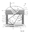
In an alternative embodiment as shown in FIGS. 5C-5D , the structure of the backside light mirror 102 is provided in addition to the structure of the backside light guide 302, with the backside light guide 302 mounted between the backside light mirror 102 and the color filter layer 52. In this implementation, the backside light mirror 102 and backside light guide 302 may be made of same or different reflective materials (preferably reflective metal materials). Furthermore, in this implementation reflections of rays or photons are made with respect to the underside reflective surface surface of the backside light mirror 102.
The configuration of the photosensitive structures and charge storage and transistor structures in FIGS. 1-5D is only one example of a pixel configuration. The backside light mirror and backside light guide as described above are equally useful in connection with pixels having configurations other than as illustrated in FIGS. 1-5D . For example, the pixel may instead have a configuration as taught by U.S. Pat. Nos. 8,436,440, 8,513,761 and 8,735,208, the disclosures of which are incorporated by reference.
The foregoing description has provided by way of exemplary and non-limiting examples a full and informative description of the exemplary embodiment of this invention. However, various modifications and adaptations may become apparent to those skilled in the relevant arts in view of the foregoing description, when read in conjunction with the accompanying drawings and the appended claims. However, all such and similar modifications of the teachings of this invention will still fall within the scope of this invention as defined in the appended claims.
Claims (20)
1. A photosensor, comprising:
a semiconductor substrate layer having a front side and a back side;
an isolation structure delimiting an active region of the semiconductor substrate layer;
a charge collecting region within the active region;
a charge transfer circuit within the active region at the front side of the semiconductor substrate layer; and
a reflecting mirror mounted at the back side of the semiconductor substrate layer, said reflecting mirror including a pupil opening configured to admit light into the active region at the back side and including an underside reflective surface configured to reflect light received from the active region back into the active region.
2. The photosensor of claim 1 , further including an antireflective coating layer positioned between the back side of the semiconductor substrate layer and the reflecting mirror.
3. The photosensor of claim 1 , wherein the reflecting mirror comprises a layer of reflective material.
4. The photosensor of claim 3 , wherein the reflective material is a metal material.
5. The photosensor of claim 4 , wherein the metal material is selected from the group consisting of: aluminum, titanium, titanium nitride, titanium alloy, tungsten, chromium, copper.
6. The photosensor of claim 1 , wherein the reflecting mirror further comprises a light pipe aligned with the pupil opening and including a reflective conical surface configured to reflect light through the pupil opening.
7. The photosensor of claim 6 , wherein the reflective conical surface is defined at an interface between a first transparent material having a first index of refraction and a second transparent material having a second index of refraction.
8. The photosensor of claim 6 , wherein the reflective conical surface is defined by a frustoconical aperture formed in a layer of reflective material, said frustoconical aperture filled with a transparent material.
9. The photosensor of claim 8 , wherein the reflective material is a metal material.
10. The photosensor of claim 9 , wherein the metal material is selected from the group consisting of: aluminum, titanium, titanium nitride, titanium alloy, tungsten, chromium, copper.
11. The photosensor of claim 8 , wherein the underside reflective surface of the reflecting mirror is formed from an additional layer of reflective material layer positioned between the layer of reflective material and the layer of reflective material having the frustoconical aperture.
12. The photosensor of claim 8 , wherein said pupil opening is provided at a narrowest portion of the frustoconical aperture.
13. The photosensor of claim 8 , further comprising a microlens mounted over the frustoconical aperture and configured to collect said light.
14. The photosensor of claim 6 , further comprising a microlens mounted over the light pipe and configured to collect said light.
15. The photosensor of claim 1 , further comprising a microlens mounted over the pupil opening and configured to collect said light.
16. A photosensor, comprising:
a semiconductor substrate layer having a front side and a back side;
an isolation structure delimiting an active region of the semiconductor substrate layer;
a charge collecting region within the active region;
a charge transfer circuit within the active region at the front side of the semiconductor substrate layer;
an antireflective coating layer mounted to the back side of the semiconductor substrate layer; and
a first layer made of a reflective metal material mounted to the antireflective coating layer, said first layer including a pupil opening configured to admit light into the active region at the back side, and wherein an underside reflective surface of said first layer is configured to reflect light received from the active region back into the active region.
17. The photosensor of claim 16 , further comprising:
a second layer made of a reflective metal material mounted to the first layer, said second layer including a frustoconical aperture aligned with the pupil opening and filled with a transparent material, said frustoconical aperture defining a reflective conical surface configured to reflect light through the pupil opening.
18. The photosensor of claim 16 , further comprising a microlens mounted over the pupil opening and configured to collect said light.
19. A photosensor, comprising:
a semiconductor substrate layer having a front side and a back side;
an isolation structure delimiting an active region of the semiconductor substrate layer;
a charge collecting region within the active region;
a charge transfer circuit within the active region at the front side of the semiconductor substrate layer;
an antireflective coating layer mounted to the back side of the semiconductor substrate layer; and
a layer made of a reflective metal material mounted to the antireflective coating layer, said layer including a frustoconical aperture filled with a transparent material, said frustoconical aperture defining a reflective conical surface configured to reflect light into the active region at the back side, and wherein an underside reflective surface of said layer is configured to reflect light received from the active region back into the active region.
20. The photosensor of claim 19 , further comprising a microlens mounted over the frustoconical aperture and configured to collect said light.
Priority Applications (1)
| Application Number | Priority Date | Filing Date | Title |
|---|---|---|---|
| US15/198,824 US10192917B2 (en) | 2016-06-30 | 2016-06-30 | Backside illuminated photosensor element with light pipe and light mirror structures |
Applications Claiming Priority (1)
| Application Number | Priority Date | Filing Date | Title |
|---|---|---|---|
| US15/198,824 US10192917B2 (en) | 2016-06-30 | 2016-06-30 | Backside illuminated photosensor element with light pipe and light mirror structures |
Publications (2)
| Publication Number | Publication Date |
|---|---|
| US20180006072A1 US20180006072A1 (en) | 2018-01-04 |
| US10192917B2 true US10192917B2 (en) | 2019-01-29 |
Family
ID=60807820
Family Applications (1)
| Application Number | Title | Priority Date | Filing Date |
|---|---|---|---|
| US15/198,824 Active 2037-07-11 US10192917B2 (en) | 2016-06-30 | 2016-06-30 | Backside illuminated photosensor element with light pipe and light mirror structures |
Country Status (1)
| Country | Link |
|---|---|
| US (1) | US10192917B2 (en) |
Cited By (1)
| Publication number | Priority date | Publication date | Assignee | Title |
|---|---|---|---|---|
| US11515348B2 (en) | 2019-11-06 | 2022-11-29 | Samsung Electronics Co., Ltd. | Image sensor |
Families Citing this family (11)
| Publication number | Priority date | Publication date | Assignee | Title |
|---|---|---|---|---|
| KR20180034750A (en) * | 2016-09-26 | 2018-04-05 | 삼성디스플레이 주식회사 | Display device and driving method thereof |
| JP6648666B2 (en) * | 2016-09-30 | 2020-02-14 | 株式会社ニコン | Image sensor and focus adjustment device |
| JP2020126961A (en) * | 2019-02-06 | 2020-08-20 | ソニーセミコンダクタソリューションズ株式会社 | Imaging apparatus and imaging system |
| US10797090B2 (en) * | 2019-02-27 | 2020-10-06 | Semiconductor Components Industries, Llc | Image sensor with near-infrared and visible light phase detection pixels |
| US10854653B2 (en) * | 2019-04-10 | 2020-12-01 | Semiconductor Components Industries, Llc | Imaging systems with improved near-infrared detection pixels |
| US20220246659A1 (en) * | 2019-07-11 | 2022-08-04 | Sony Semiconductor Solutions Corporation | Imaging device and imaging apparatus |
| JP2021015869A (en) * | 2019-07-11 | 2021-02-12 | ソニーセミコンダクタソリューションズ株式会社 | Imaging element and image device |
| JP2021090022A (en) * | 2019-12-06 | 2021-06-10 | ソニーセミコンダクタソリューションズ株式会社 | Image pickup device and imaging apparatus |
| WO2022019307A1 (en) * | 2020-07-22 | 2022-01-27 | 国立大学法人静岡大学 | Photoelectric conversion element |
| US11670651B2 (en) * | 2020-11-13 | 2023-06-06 | Taiwan Semiconductor Manufacturing Company, Ltd. | Pixel array including octagon pixel sensors |
| CN116636018A (en) * | 2021-01-13 | 2023-08-22 | 索尼半导体解决方案公司 | Solid-state imaging device |
Citations (13)
| Publication number | Priority date | Publication date | Assignee | Title |
|---|---|---|---|---|
| US7524694B2 (en) | 2005-12-16 | 2009-04-28 | International Business Machines Corporation | Funneled light pipe for pixel sensors |
| US20090200625A1 (en) * | 2008-02-08 | 2009-08-13 | Omnivision Technologies, Inc. | Backside illuminated image sensor having deep light reflective trenches |
| US8093673B2 (en) * | 2009-07-31 | 2012-01-10 | Aptina Imaging Corporation | Columnated backside illumination structure |
| US20120261783A1 (en) | 2011-04-12 | 2012-10-18 | Stmicroelectronics (Crolles 2) Sas | Back-side illuminated image sensor provided with a transparent electrode |
| US20120261670A1 (en) | 2011-04-12 | 2012-10-18 | Stmicroelectronics (Crolles 2) Sas | Back-side illuminated image sensor with a junction insulation |
| US20120326256A1 (en) * | 2011-02-07 | 2012-12-27 | Kenneth Edward Salsman | Spectrally tuned plasmonic light collectors |
| US8436440B2 (en) | 2009-11-10 | 2013-05-07 | Stmicroelectronics (Crolles 2) Sas | Method for forming a back-side illuminated image sensor |
| US20130193538A1 (en) * | 2012-01-31 | 2013-08-01 | Taiwan Semiconductor Manufacturing Company, Ltd. | Methods and Apparatus for an Improved Reflectivity Optical Grid for Image Sensors |
| US8513761B2 (en) | 2009-02-05 | 2013-08-20 | Stmicroelectronics (Grenoble) Sas | Backside illumination semiconductor image sensor |
| US20140077323A1 (en) * | 2012-09-19 | 2014-03-20 | Aptina Imaging Corporation | Imaging systems with backside illuminated near infrared imaging pixels |
| US8735208B2 (en) | 2011-04-12 | 2014-05-27 | Stmicroelectronics S.A. | Method for forming a back-side illuminated image sensor |
| US20140197509A1 (en) * | 2009-09-17 | 2014-07-17 | Sionyx, Inc. | Photosensitive imaging devices and associated methods |
| US8847344B2 (en) | 2011-06-06 | 2014-09-30 | STMicroelectronics (Croles 2) SAS | Process for fabricating a backside-illuminated imaging device and corresponding device |
-
2016
- 2016-06-30 US US15/198,824 patent/US10192917B2/en active Active
Patent Citations (13)
| Publication number | Priority date | Publication date | Assignee | Title |
|---|---|---|---|---|
| US7524694B2 (en) | 2005-12-16 | 2009-04-28 | International Business Machines Corporation | Funneled light pipe for pixel sensors |
| US20090200625A1 (en) * | 2008-02-08 | 2009-08-13 | Omnivision Technologies, Inc. | Backside illuminated image sensor having deep light reflective trenches |
| US8513761B2 (en) | 2009-02-05 | 2013-08-20 | Stmicroelectronics (Grenoble) Sas | Backside illumination semiconductor image sensor |
| US8093673B2 (en) * | 2009-07-31 | 2012-01-10 | Aptina Imaging Corporation | Columnated backside illumination structure |
| US20140197509A1 (en) * | 2009-09-17 | 2014-07-17 | Sionyx, Inc. | Photosensitive imaging devices and associated methods |
| US8436440B2 (en) | 2009-11-10 | 2013-05-07 | Stmicroelectronics (Crolles 2) Sas | Method for forming a back-side illuminated image sensor |
| US20120326256A1 (en) * | 2011-02-07 | 2012-12-27 | Kenneth Edward Salsman | Spectrally tuned plasmonic light collectors |
| US20120261783A1 (en) | 2011-04-12 | 2012-10-18 | Stmicroelectronics (Crolles 2) Sas | Back-side illuminated image sensor provided with a transparent electrode |
| US8735208B2 (en) | 2011-04-12 | 2014-05-27 | Stmicroelectronics S.A. | Method for forming a back-side illuminated image sensor |
| US20120261670A1 (en) | 2011-04-12 | 2012-10-18 | Stmicroelectronics (Crolles 2) Sas | Back-side illuminated image sensor with a junction insulation |
| US8847344B2 (en) | 2011-06-06 | 2014-09-30 | STMicroelectronics (Croles 2) SAS | Process for fabricating a backside-illuminated imaging device and corresponding device |
| US20130193538A1 (en) * | 2012-01-31 | 2013-08-01 | Taiwan Semiconductor Manufacturing Company, Ltd. | Methods and Apparatus for an Improved Reflectivity Optical Grid for Image Sensors |
| US20140077323A1 (en) * | 2012-09-19 | 2014-03-20 | Aptina Imaging Corporation | Imaging systems with backside illuminated near infrared imaging pixels |
Cited By (1)
| Publication number | Priority date | Publication date | Assignee | Title |
|---|---|---|---|---|
| US11515348B2 (en) | 2019-11-06 | 2022-11-29 | Samsung Electronics Co., Ltd. | Image sensor |
Also Published As
| Publication number | Publication date |
|---|---|
| US20180006072A1 (en) | 2018-01-04 |
Similar Documents
| Publication | Publication Date | Title |
|---|---|---|
| US10192917B2 (en) | Backside illuminated photosensor element with light pipe and light mirror structures | |
| KR102204728B1 (en) | Spad image sensor and associated fabricating method | |
| US11791360B2 (en) | Photoelectric conversion apparatus and camera | |
| US7488615B2 (en) | Method of manufacturing a solid-state imaging device | |
| US7608906B2 (en) | Simultaneous unipolar multispectral integrated technology (SUMIT) detectors | |
| KR20190037186A (en) | Back-side deep trench isolation (bdti) structure for pinned photodiode image sensor | |
| US8212901B2 (en) | Backside illuminated imaging sensor with reduced leakage photodiode | |
| KR20080050434A (en) | Solid-state imager and formation method using anti-reflective film for optical crosstalk reduction | |
| US10051218B1 (en) | Stacked image sensor pixel cell with in-pixel vertical channel transfer transistor and reflective structure | |
| CN108010927A (en) | Photoelectric conversion device and image picking system | |
| US20150349001A1 (en) | Semiconductor isolation structure and manufacturing method thereof | |
| US11686614B2 (en) | Photodetecting device for detecting different wavelengths | |
| US20180342543A1 (en) | Backside illuminated cmos image sensor and method of fabricating the same | |
| US11276716B2 (en) | Image sensor with improved near-infrared (NIR) radiation phase-detection autofocus (PDAF) performance | |
| US11784202B2 (en) | Image sensor | |
| US20230290672A1 (en) | Image sensor with dual trench isolation structure | |
| KR20190055766A (en) | Light blocking layer for image sensor device | |
| CN111834382A (en) | Solid-state imaging device | |
| US20230395640A1 (en) | Dielectric structure overlying image sensor element to increase quantum efficiency | |
| US10109671B2 (en) | Photodiode array structure for cross talk suppression | |
| US20110140168A1 (en) | Avalanche phototector with integrated micro lens | |
| US20090200588A1 (en) | Backside illuminated imaging sensor with light reflecting transfer gate | |
| US9769398B2 (en) | Image sensor with large-area global shutter contact | |
| CN211529954U (en) | TOF sensor having highly light-transmissive electrode structure and imaging apparatus | |
| KR102616543B1 (en) | Light blocking layer for image sensor device |
Legal Events
| Date | Code | Title | Description |
|---|---|---|---|
| AS | Assignment |
Owner name: STMICROELECTRONICS (CROLLES 2) SAS, FRANCE Free format text: ASSIGNMENT OF ASSIGNORS INTEREST;ASSIGNORS:ROY, FRANCOIS;MAMDY, BASTIEN;REEL/FRAME:039057/0879 Effective date: 20160616 |
|
| STCF | Information on status: patent grant |
Free format text: PATENTED CASE |
|
| MAFP | Maintenance fee payment |
Free format text: PAYMENT OF MAINTENANCE FEE, 4TH YEAR, LARGE ENTITY (ORIGINAL EVENT CODE: M1551); ENTITY STATUS OF PATENT OWNER: LARGE ENTITY Year of fee payment: 4 |