US10186471B2 - Solid-state drive device - Google Patents
Solid-state drive device Download PDFInfo
- Publication number
- US10186471B2 US10186471B2 US15/651,106 US201715651106A US10186471B2 US 10186471 B2 US10186471 B2 US 10186471B2 US 201715651106 A US201715651106 A US 201715651106A US 10186471 B2 US10186471 B2 US 10186471B2
- Authority
- US
- United States
- Prior art keywords
- circuit board
- memory chips
- solid
- drive device
- state drive
- Prior art date
- Legal status (The legal status is an assumption and is not a legal conclusion. Google has not performed a legal analysis and makes no representation as to the accuracy of the status listed.)
- Active
Links
Images


Classifications
-
- H—ELECTRICITY
- H10—SEMICONDUCTOR DEVICES; ELECTRIC SOLID-STATE DEVICES NOT OTHERWISE PROVIDED FOR
- H10W—GENERIC PACKAGES, INTERCONNECTIONS, CONNECTORS OR OTHER CONSTRUCTIONAL DETAILS OF DEVICES COVERED BY CLASS H10
- H10W40/00—Arrangements for thermal protection or thermal control
- H10W40/20—Arrangements for cooling
- H10W40/22—Arrangements for cooling characterised by their shape, e.g. having conical or cylindrical projections
-
- H01L23/3675—
-
- G—PHYSICS
- G11—INFORMATION STORAGE
- G11B—INFORMATION STORAGE BASED ON RELATIVE MOVEMENT BETWEEN RECORD CARRIER AND TRANSDUCER
- G11B33/00—Constructional parts, details or accessories not provided for in the other groups of this subclass
- G11B33/12—Disposition of constructional parts in the apparatus, e.g. of power supply, of modules
- G11B33/121—Disposition of constructional parts in the apparatus, e.g. of power supply, of modules the apparatus comprising a single recording/reproducing device
-
- H—ELECTRICITY
- H05—ELECTRIC TECHNIQUES NOT OTHERWISE PROVIDED FOR
- H05K—PRINTED CIRCUITS; CASINGS OR CONSTRUCTIONAL DETAILS OF ELECTRIC APPARATUS; MANUFACTURE OF ASSEMBLAGES OF ELECTRICAL COMPONENTS
- H05K7/00—Constructional details common to different types of electric apparatus
- H05K7/20—Modifications to facilitate cooling, ventilating, or heating
- H05K7/20709—Modifications to facilitate cooling, ventilating, or heating for server racks or cabinets; for data centers, e.g. 19-inch computer racks
-
- G—PHYSICS
- G06—COMPUTING OR CALCULATING; COUNTING
- G06F—ELECTRIC DIGITAL DATA PROCESSING
- G06F1/00—Details not covered by groups G06F3/00 - G06F13/00 and G06F21/00
- G06F1/16—Constructional details or arrangements
- G06F1/18—Packaging or power distribution
-
- G—PHYSICS
- G06—COMPUTING OR CALCULATING; COUNTING
- G06F—ELECTRIC DIGITAL DATA PROCESSING
- G06F1/00—Details not covered by groups G06F3/00 - G06F13/00 and G06F21/00
- G06F1/16—Constructional details or arrangements
- G06F1/20—Cooling means
-
- G—PHYSICS
- G11—INFORMATION STORAGE
- G11B—INFORMATION STORAGE BASED ON RELATIVE MOVEMENT BETWEEN RECORD CARRIER AND TRANSDUCER
- G11B33/00—Constructional parts, details or accessories not provided for in the other groups of this subclass
- G11B33/14—Reducing influence of physical parameters, e.g. temperature change, moisture, dust
- G11B33/1406—Reducing the influence of the temperature
- G11B33/1413—Reducing the influence of the temperature by fluid cooling
- G11B33/142—Reducing the influence of the temperature by fluid cooling by air cooling
-
- G—PHYSICS
- G11—INFORMATION STORAGE
- G11C—STATIC STORES
- G11C5/00—Details of stores covered by group G11C11/00
-
- H01L23/04—
-
- H01L23/42—
-
- H—ELECTRICITY
- H05—ELECTRIC TECHNIQUES NOT OTHERWISE PROVIDED FOR
- H05K—PRINTED CIRCUITS; CASINGS OR CONSTRUCTIONAL DETAILS OF ELECTRIC APPARATUS; MANUFACTURE OF ASSEMBLAGES OF ELECTRICAL COMPONENTS
- H05K1/00—Printed circuits
- H05K1/02—Details
- H05K1/0201—Thermal arrangements, e.g. for cooling, heating or preventing overheating
-
- H—ELECTRICITY
- H05—ELECTRIC TECHNIQUES NOT OTHERWISE PROVIDED FOR
- H05K—PRINTED CIRCUITS; CASINGS OR CONSTRUCTIONAL DETAILS OF ELECTRIC APPARATUS; MANUFACTURE OF ASSEMBLAGES OF ELECTRICAL COMPONENTS
- H05K7/00—Constructional details common to different types of electric apparatus
- H05K7/20—Modifications to facilitate cooling, ventilating, or heating
- H05K7/20709—Modifications to facilitate cooling, ventilating, or heating for server racks or cabinets; for data centers, e.g. 19-inch computer racks
- H05K7/20718—Forced ventilation of a gaseous coolant
- H05K7/20727—Forced ventilation of a gaseous coolant within server blades for removing heat from heat source
-
- H—ELECTRICITY
- H10—SEMICONDUCTOR DEVICES; ELECTRIC SOLID-STATE DEVICES NOT OTHERWISE PROVIDED FOR
- H10W—GENERIC PACKAGES, INTERCONNECTIONS, CONNECTORS OR OTHER CONSTRUCTIONAL DETAILS OF DEVICES COVERED BY CLASS H10
- H10W40/00—Arrangements for thermal protection or thermal control
- H10W40/70—Fillings or auxiliary members in containers or in encapsulations for thermal protection or control
-
- H—ELECTRICITY
- H10—SEMICONDUCTOR DEVICES; ELECTRIC SOLID-STATE DEVICES NOT OTHERWISE PROVIDED FOR
- H10W—GENERIC PACKAGES, INTERCONNECTIONS, CONNECTORS OR OTHER CONSTRUCTIONAL DETAILS OF DEVICES COVERED BY CLASS H10
- H10W76/00—Containers; Fillings or auxiliary members therefor; Seals
- H10W76/10—Containers or parts thereof
- H10W76/12—Containers or parts thereof characterised by their shape
-
- H—ELECTRICITY
- H05—ELECTRIC TECHNIQUES NOT OTHERWISE PROVIDED FOR
- H05K—PRINTED CIRCUITS; CASINGS OR CONSTRUCTIONAL DETAILS OF ELECTRIC APPARATUS; MANUFACTURE OF ASSEMBLAGES OF ELECTRICAL COMPONENTS
- H05K2201/00—Indexing scheme relating to printed circuits covered by H05K1/00
- H05K2201/10—Details of components or other objects attached to or integrated in a printed circuit board
- H05K2201/10007—Types of components
- H05K2201/10159—Memory
Definitions
- the present invention relates to a solid-state drive device, and in particular to a solid-state drive device with improved heat dissipation.
- a conventional solid-state drive device utilizes a metal housing to remove the heat generated by the controller and the memory chips.
- the heat generated by the solid-state drive device cannot be sufficiently removed by only the metal housing.
- a solid-state drive device in one embodiment, includes a housing, a first circuit board, and a second circuit board.
- the housing includes a first side and a second side. The first side is opposite to the second side. At least one first ventilation hole is formed on the first side. At least one second ventilation hole is formed on the second side.
- the first circuit board is disposed in the housing.
- the second circuit board is disposed in the housing. The second circuit board is coupled to the first circuit board.
- a gap is formed between the first circuit board and the second circuit board. The first ventilation hole and the second ventilation hole correspond to the gap.
- the solid-state drive device further comprises a controller.
- the housing comprises a first member and a second member.
- the first member is combined with the second member.
- the controller is disposed on the first circuit board.
- the controller faces the first member.
- the controller is thermally connected to the first member by conduction.
- the solid-state drive device further comprises a plurality of first memory chips and a plurality of second memory chips.
- the first memory chips are disposed on the first circuit board.
- the second memory chips are disposed on the second circuit board. At least a portion of the first memory chips and at least a portion of the second memory chips are disposed in the gap.
- At least a portion of the first memory chips face the first member, and at least a portion of the second memory chips face the second member.
- At least a portion of the first memory chips and at least a portion of the second memory chips are located in the gap, and at least a portion of the first memory chips correspond to at least a portion of the second memory chips in the gap.
- the second memory chips comprise a second memory chip array, and at least a second flow path is defined by the second memory chip array.
- the first memory chips comprise a first memory chip array, at least a first flow path is defined by the first memory chip array, and the first flow path corresponds to the second flow path.
- the solid-state drive device further comprises a plurality of conversion head screws, and a plurality of fastening screws, each conversion head screw comprises a convex portion and a concave portion, the convex portion affixes the first circuit board to the first member, and the fastening screw affixes the second circuit board to the concave portion.
- the solid-state drive device further comprises a plurality of fixing screws, and the fixing screws directly affix the first member to the second member.
- the first member comprises a recess and a heat dissipation structure
- the recess is formed on an inner surface of the first member and faces the controller
- the heat dissipation structure is formed on an outer surface of the first member.
- the first ventilation hole and the second ventilation hole correspond to the gap. Air flow enters the housing and removes the heat from the heat sources (such as memory chips) which are located in the gap. The heat inside the housing is removed by convection, and heat dissipation efficiency is improved.
- the heat sources such as memory chips
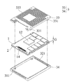
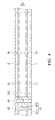
- FIG. 1 is a perspective view of a solid-state drive device of an embodiment of the invention
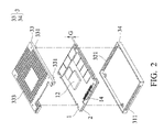
- FIG. 2 is an exploded view of the solid-state drive device of the embodiment of the invention.
- FIG. 3A shows details of the first circuit board and the second circuit board from one side
- FIG. 3B shows details of the first circuit board and the second circuit board from the other side
- FIG. 4 is a side view of the first circuit board and the second circuit board
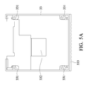
- FIG. 5A shows the inner surface of the first member of an embodiment of the invention
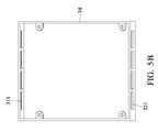
- FIG. 5B shows the inner surface of the second member of an embodiment of the invention.
- FIG. 6 shows an outer surface of the first member of an embodiment of the invention.
- FIG. 1 is a perspective view of a solid-state drive device of an embodiment of the invention.
- FIG. 2 is an exploded view of the solid-state drive device of the embodiment of the invention.
- the solid-state drive device includes a housing 3 , a first circuit board 1 and a second circuit board 2 .
- the housing 3 includes a first side 31 and a second side 32 .
- the first side 31 is opposite to the second side 32 .
- At least one first ventilation hole 311 is formed on the first side 31 .
- At least one second ventilation hole 321 is formed on the second side 32 .
- the first circuit board 1 is disposed in the housing 3 .
- the second circuit board 2 is disposed in the housing 3 .
- the second circuit board 2 is coupled to the first circuit board 1 .
- a gap G is formed between the first circuit board 1 and the second circuit board 2 .
- the first ventilation hole 311 and the second ventilation hole 321 correspond to the gap G.
- the first ventilation hole 311 and the second ventilation hole 321 correspond to the gap G.
- air flow enters the housing 3 through the first ventilation hole 311 and leaves the housing 3 through the second ventilation hole 321 .
- the air flow enters the housing 3 through the second ventilation hole 321 and leaves the housing 3 through the first ventilation hole 311 .
- the air flow can be impelled by a blower or a fan.
- the air flow enters the housing 3 and removes the heat from the heat sources (such as memory chips) which are located in the gap G.
- the heat inside the housing 3 is removed by convection, and heat dissipation efficiency is improved.
- the number, shape and dimensions of the first ventilation hole 311 and the second ventilation hole 321 can be modified. The disclosure is not meant to restrict the invention.
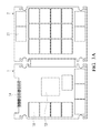
- FIG. 3A shows details of the first circuit board 1 and the second circuit board 2 from one side.
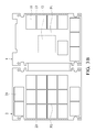
- FIG. 3B shows details of the first circuit board 1 and the second circuit board 2 from the other side.
- the solid-state drive device further comprises a controller 12 and a gold finger area 14 .
- the housing 3 comprises a first member 33 and a second member 34 .
- the first member 33 is combined with the second member 34 .
- the controller 12 is disposed on the first circuit board 1 .
- the controller 12 faces the first member 33 .
- the controller 12 is thermally connected to the first member 33 by conduction.
- the controller 12 is thermally connected to the first member 33 by thermal glue, or a thermal pad, or by utilizing the thermal glue and the thermal pad simultaneously.
- the controller 12 can be in direct contact with the first member 33 .
- the heat generated by the controller 12 is removed by the housing 3 , and the housing is made of metal.
- the solid-state drive device further comprises a plurality of first memory chips 11 and a plurality of second memory chips 21 .
- the first memory chips 11 are disposed on the first circuit board 1 .
- the second memory chips 21 are disposed on the second circuit board 2 .
- FIG. 4 is a side view of the first circuit board 1 and the second circuit board 2 .
- at least a portion of the first memory chips 11 and at least a portion of the second memory chips 21 are disposed in the gap G.
- at least a portion of the first memory chips 11 face the first member 33 , and the heat generated thereby are removed by conduction via the first member 33 .
- At least a portion of the second memory chips 21 face the second member 34 , and the heat generated thereby are removed by conduction via the second member 34 .
- the disclosure is not meant to restrict the invention.
- all of the first memory chips 11 are located in the gap G.
- all of the second memory chips 21 face the second member 34 .
- the heat dissipation due to convection inside the housing 3 is improved by the arrangement of the first memory chips 11 and the second memory chips 21 .
- the first memory chips 11 and the second memory chips 21 are located in the gap, and at least a portion of the first memory chips 11 correspond to at least a portion of the second memory chips 21 in the gap.
- the second memory chips 21 comprise a second memory chip array 23 , and at least a second flow path P 2 is defined by the second memory chip array 23 .
- the first memory chips 11 comprise a first memory chip array 13 , and at least a first flow path P 1 is defined by the first memory chip array 13 .
- the first flow path P 1 corresponds to the second flow path P 2 .
- a large flow path is formed by combining the first flow path P 1 and the second flow path P 2 .
- the air flow that travels in the large flow path has an increased flow rate, and provides improved heat dissipation efficiency.
- FIG. 5A shows the inner surface of the first member 33 of an embodiment of the invention.
- FIG. 5B shows the inner surface of the second member 34 of an embodiment of the invention.
- the solid-state drive device further comprises a plurality of conversion head screws 41 , and a plurality of fastening screws 42 .
- Each conversion head screw 41 comprises a convex portion 411 and a concave portion 412 .
- the convex portion 411 affixes the first circuit board 1 to the first member 33
- the fastening screw 42 affixes the second circuit board 2 to the concave portion 412 .
- the solid-state drive device further comprises a plurality of fixing screws 43 , and the fixing screws 43 directly affix the first member 33 to the second member 34 .
- a plurality of fixing holes are formed on the first member 33 to be connected with of the fixing screws 43 .
- the first member 33 comprises a recess 332 .
- the recess 332 is formed on the inner surface of the first member 33 and faces the controller 12 . Because the height of the controller 12 is greater than the height of the memory chip, the recess 332 improves the smoothness and the appearance of the solid-state drive device.
- FIG. 6 shows an outer surface of the first member 33 of an embodiment of the invention.
- a heat dissipation structure 333 is formed on the outer surface of the first member 33 .
- the heat dissipation structure 333 comprises concave and convex structures to provide improved heat dissipation efficiency.
- the temperature of the controller 12 is greater than that of the memory chips.
- the heat dissipation structure 333 formed on the first member 33 removes the heat generated by the controller 12 .
- the ventilation holes of a plurality of solid-state drive devices correspond to each other, and the ventilation holes are communicated in series to form one flow path to remove heat from the solid-state drive devices.
Landscapes
- Engineering & Computer Science (AREA)
- Physics & Mathematics (AREA)
- General Engineering & Computer Science (AREA)
- Microelectronics & Electronic Packaging (AREA)
- Theoretical Computer Science (AREA)
- Thermal Sciences (AREA)
- Computer Hardware Design (AREA)
- Human Computer Interaction (AREA)
- General Physics & Mathematics (AREA)
- Power Engineering (AREA)
- Cooling Or The Like Of Electrical Apparatus (AREA)
- Cooling Or The Like Of Semiconductors Or Solid State Devices (AREA)
Abstract
Description
Claims (19)
Applications Claiming Priority (3)
| Application Number | Priority Date | Filing Date | Title |
|---|---|---|---|
| CN201611079323.X | 2016-11-30 | ||
| CN201611079323 | 2016-11-30 | ||
| CN201611079323.XA CN108133722B (en) | 2016-11-30 | 2016-11-30 | solid state drive |
Publications (2)
| Publication Number | Publication Date |
|---|---|
| US20180151469A1 US20180151469A1 (en) | 2018-05-31 |
| US10186471B2 true US10186471B2 (en) | 2019-01-22 |
Family
ID=62190463
Family Applications (1)
| Application Number | Title | Priority Date | Filing Date |
|---|---|---|---|
| US15/651,106 Active US10186471B2 (en) | 2016-11-30 | 2017-07-17 | Solid-state drive device |
Country Status (3)
| Country | Link |
|---|---|
| US (1) | US10186471B2 (en) |
| CN (1) | CN108133722B (en) |
| TW (1) | TWI633540B (en) |
Cited By (8)
| Publication number | Priority date | Publication date | Assignee | Title |
|---|---|---|---|---|
| US10477706B1 (en) * | 2019-03-07 | 2019-11-12 | Shannon Systems Ltd. | Solid state memory device |
| US10798839B2 (en) | 2019-02-13 | 2020-10-06 | Cisco Technology, Inc. | Thermal management cage for a solid state drive |
| US20210385956A1 (en) * | 2020-06-09 | 2021-12-09 | Samsung Electronics Co., Ltd. | Memory device and electronic device including the same |
| US20220369515A1 (en) * | 2021-05-14 | 2022-11-17 | Shannon Systems Ltd. | Add-in module |
| US20220377915A1 (en) * | 2021-05-18 | 2022-11-24 | Shannon Systems Ltd. | Electronic device with storage function |
| US20240121921A1 (en) * | 2022-10-09 | 2024-04-11 | Shannon Systems Ltd. | Server apparatus and solid-state storage device thereof |
| US12376262B2 (en) * | 2022-10-09 | 2025-07-29 | Shannon Systems Ltd. | Server apparatus and solid-state storage device thereof |
| USD1106195S1 (en) * | 2023-06-25 | 2025-12-16 | Dapustor Corporation | Solid-state drive |
Families Citing this family (3)
| Publication number | Priority date | Publication date | Assignee | Title |
|---|---|---|---|---|
| JP2020119980A (en) * | 2019-01-23 | 2020-08-06 | キオクシア株式会社 | Electronic device |
| CN110780719B (en) * | 2019-09-25 | 2021-07-06 | 苏州浪潮智能科技有限公司 | A server cooling device |
| CN120071979A (en) * | 2023-11-28 | 2025-05-30 | 上海宝存信息科技有限公司 | Electronic device |
Citations (20)
| Publication number | Priority date | Publication date | Assignee | Title |
|---|---|---|---|---|
| US5361188A (en) * | 1990-10-24 | 1994-11-01 | Hitachi Ltd. | Cooling apparatus of electronic equipment |
| US20050124221A1 (en) * | 2003-12-05 | 2005-06-09 | Yu-Kai Lin | Plasma display |
| US20050286221A1 (en) * | 2004-06-23 | 2005-12-29 | Shunsuke Yamana | Storage device system and cooling structure for logic circuit board for storage device system |
| US20090086430A1 (en) * | 2007-09-27 | 2009-04-02 | Samsung Electronics Co., Ltd. | Cooling unit and display apparatus having the same |
| TW201016085A (en) | 2008-09-09 | 2010-04-16 | Samsung Electronics Co Ltd | Circuit boards, connectors, cases, circuit board assemblies, case assemblies, devices and methods of manufacturing the same |
| TW201027528A (en) | 2009-01-09 | 2010-07-16 | Super Team Technology Co Ltd | Structure of solid state disk |
| US7782615B1 (en) * | 2009-03-26 | 2010-08-24 | Hon Hai Precision Industry Co., Ltd. | Electronic device and cooling system thereof |
| US20110199748A1 (en) * | 2010-02-17 | 2011-08-18 | Kabushiki Kaisha Toshiba | Semiconductor storage device and electronic device |
| CN202058453U (en) | 2011-04-01 | 2011-11-30 | 原昇科技有限公司 | Solid state drive without screws |
| TW201205589A (en) | 2010-07-30 | 2012-02-01 | Apacer Technology Inc | Stack structure of solid state drive module |
| US20130044431A1 (en) * | 2011-08-18 | 2013-02-21 | Harris Corporation | Liquid cooling of stacked die through substrate lamination |
| US20130083481A1 (en) * | 2011-09-29 | 2013-04-04 | Hitachi, Ltd. | Cooling system for electronic device |
| US20130155600A1 (en) * | 2011-12-15 | 2013-06-20 | Peter G. Ross | Reconfigurable Shelf For Computing Modules |
| US20130329364A1 (en) * | 2012-06-08 | 2013-12-12 | Alaxala Networks Corporation | Network communication device |
| CN203689294U (en) | 2014-02-20 | 2014-07-02 | 新疆旗安科技有限公司 | Professional cloud storage server for big data |
| TWM517895U (en) | 2015-09-25 | 2016-02-21 | 威剛科技股份有限公司 | Solid state hard disk structure |
| US20170099746A1 (en) * | 2015-10-01 | 2017-04-06 | Microsoft Technology Licensing, Llc | Layered airflow cooling for electronic components |
| US9717160B2 (en) * | 2012-07-26 | 2017-07-25 | Nec Corporation | High-density server with redundant power source for server modules |
| US9750128B2 (en) * | 2015-03-11 | 2017-08-29 | Fujitsu Limited | Unit device |
| US20180049349A1 (en) * | 2016-08-11 | 2018-02-15 | Seagate Technology Llc | Ssd internal thermal transfer element |
-
2016
- 2016-11-30 CN CN201611079323.XA patent/CN108133722B/en active Active
-
2017
- 2017-01-03 TW TW106100041A patent/TWI633540B/en active
- 2017-07-17 US US15/651,106 patent/US10186471B2/en active Active
Patent Citations (20)
| Publication number | Priority date | Publication date | Assignee | Title |
|---|---|---|---|---|
| US5361188A (en) * | 1990-10-24 | 1994-11-01 | Hitachi Ltd. | Cooling apparatus of electronic equipment |
| US20050124221A1 (en) * | 2003-12-05 | 2005-06-09 | Yu-Kai Lin | Plasma display |
| US20050286221A1 (en) * | 2004-06-23 | 2005-12-29 | Shunsuke Yamana | Storage device system and cooling structure for logic circuit board for storage device system |
| US20090086430A1 (en) * | 2007-09-27 | 2009-04-02 | Samsung Electronics Co., Ltd. | Cooling unit and display apparatus having the same |
| TW201016085A (en) | 2008-09-09 | 2010-04-16 | Samsung Electronics Co Ltd | Circuit boards, connectors, cases, circuit board assemblies, case assemblies, devices and methods of manufacturing the same |
| TW201027528A (en) | 2009-01-09 | 2010-07-16 | Super Team Technology Co Ltd | Structure of solid state disk |
| US7782615B1 (en) * | 2009-03-26 | 2010-08-24 | Hon Hai Precision Industry Co., Ltd. | Electronic device and cooling system thereof |
| US20110199748A1 (en) * | 2010-02-17 | 2011-08-18 | Kabushiki Kaisha Toshiba | Semiconductor storage device and electronic device |
| TW201205589A (en) | 2010-07-30 | 2012-02-01 | Apacer Technology Inc | Stack structure of solid state drive module |
| CN202058453U (en) | 2011-04-01 | 2011-11-30 | 原昇科技有限公司 | Solid state drive without screws |
| US20130044431A1 (en) * | 2011-08-18 | 2013-02-21 | Harris Corporation | Liquid cooling of stacked die through substrate lamination |
| US20130083481A1 (en) * | 2011-09-29 | 2013-04-04 | Hitachi, Ltd. | Cooling system for electronic device |
| US20130155600A1 (en) * | 2011-12-15 | 2013-06-20 | Peter G. Ross | Reconfigurable Shelf For Computing Modules |
| US20130329364A1 (en) * | 2012-06-08 | 2013-12-12 | Alaxala Networks Corporation | Network communication device |
| US9717160B2 (en) * | 2012-07-26 | 2017-07-25 | Nec Corporation | High-density server with redundant power source for server modules |
| CN203689294U (en) | 2014-02-20 | 2014-07-02 | 新疆旗安科技有限公司 | Professional cloud storage server for big data |
| US9750128B2 (en) * | 2015-03-11 | 2017-08-29 | Fujitsu Limited | Unit device |
| TWM517895U (en) | 2015-09-25 | 2016-02-21 | 威剛科技股份有限公司 | Solid state hard disk structure |
| US20170099746A1 (en) * | 2015-10-01 | 2017-04-06 | Microsoft Technology Licensing, Llc | Layered airflow cooling for electronic components |
| US20180049349A1 (en) * | 2016-08-11 | 2018-02-15 | Seagate Technology Llc | Ssd internal thermal transfer element |
Cited By (13)
| Publication number | Priority date | Publication date | Assignee | Title |
|---|---|---|---|---|
| US10798839B2 (en) | 2019-02-13 | 2020-10-06 | Cisco Technology, Inc. | Thermal management cage for a solid state drive |
| US10477706B1 (en) * | 2019-03-07 | 2019-11-12 | Shannon Systems Ltd. | Solid state memory device |
| US11979996B2 (en) * | 2020-06-09 | 2024-05-07 | Samsung Electronics Co., Ltd. | Memory device and electronic device including the same |
| US20210385956A1 (en) * | 2020-06-09 | 2021-12-09 | Samsung Electronics Co., Ltd. | Memory device and electronic device including the same |
| US12219721B2 (en) | 2020-06-09 | 2025-02-04 | Samsung Electronics Co., Ltd. | Memory device and electronic device including the same |
| US20220369515A1 (en) * | 2021-05-14 | 2022-11-17 | Shannon Systems Ltd. | Add-in module |
| US11632878B2 (en) * | 2021-05-14 | 2023-04-18 | Shannon Systems Ltd. | Add-in module |
| US11606866B2 (en) * | 2021-05-18 | 2023-03-14 | Shannon Systems Ltd. | Electronic device with storage function |
| US20220377915A1 (en) * | 2021-05-18 | 2022-11-24 | Shannon Systems Ltd. | Electronic device with storage function |
| US20240121921A1 (en) * | 2022-10-09 | 2024-04-11 | Shannon Systems Ltd. | Server apparatus and solid-state storage device thereof |
| US12369287B2 (en) * | 2022-10-09 | 2025-07-22 | Shannon Systems Ltd. | Server apparatus and solid-state storage device thereof |
| US12376262B2 (en) * | 2022-10-09 | 2025-07-29 | Shannon Systems Ltd. | Server apparatus and solid-state storage device thereof |
| USD1106195S1 (en) * | 2023-06-25 | 2025-12-16 | Dapustor Corporation | Solid-state drive |
Also Published As
| Publication number | Publication date |
|---|---|
| CN108133722B (en) | 2020-02-21 |
| US20180151469A1 (en) | 2018-05-31 |
| TW201822194A (en) | 2018-06-16 |
| CN108133722A (en) | 2018-06-08 |
| TWI633540B (en) | 2018-08-21 |
Similar Documents
| Publication | Publication Date | Title |
|---|---|---|
| US10186471B2 (en) | Solid-state drive device | |
| US11632878B2 (en) | Add-in module | |
| US7911798B2 (en) | Memory heat sink device provided with a larger heat dissipating area | |
| US20020126450A1 (en) | Cooling device for hard disc | |
| US8897012B2 (en) | Electronic device and heat dissipation module thereof | |
| US7640968B2 (en) | Heat dissipation device with a heat pipe | |
| US10031565B1 (en) | Heat dissipation structure of addin card | |
| US9379039B2 (en) | Heat transfer for electronic equipment | |
| US20110310565A1 (en) | Heat sink for memory module | |
| US20120162913A1 (en) | Electronic device and heat dissipation device thereof | |
| US20090303679A1 (en) | Memory module | |
| US20130083483A1 (en) | Heat dissipation device and electronic device using same | |
| US7447027B2 (en) | Hybrid heat dissipation device | |
| US12376262B2 (en) | Server apparatus and solid-state storage device thereof | |
| US12369287B2 (en) | Server apparatus and solid-state storage device thereof | |
| US20100020494A1 (en) | Heat dissipation device | |
| US20060268508A1 (en) | Heat dissipation device for a computer mother board | |
| US20180241140A1 (en) | Adapter card | |
| US9946314B1 (en) | Heat dissipation device for display card | |
| US20140174699A1 (en) | Heat dissipation assembly | |
| KR200273898Y1 (en) | Heatsink in Personal Computer | |
| CN108304048B (en) | Server and solid-state storage device thereof | |
| US20060049728A1 (en) | Computer bezel with inlet airflow guiding device | |
| US20110304992A1 (en) | Heat dissipation device | |
| US20060256520A1 (en) | Electronic device with heat dissipation module |
Legal Events
| Date | Code | Title | Description |
|---|---|---|---|
| AS | Assignment |
Owner name: SHANNON SYSTEMS LTD., CHINA Free format text: ASSIGNMENT OF ASSIGNORS INTEREST;ASSIGNOR:CHEN, XIAOYAN;REEL/FRAME:043210/0797 Effective date: 20170629 |
|
| STCF | Information on status: patent grant |
Free format text: PATENTED CASE |
|
| MAFP | Maintenance fee payment |
Free format text: PAYMENT OF MAINTENANCE FEE, 4TH YR, SMALL ENTITY (ORIGINAL EVENT CODE: M2551); ENTITY STATUS OF PATENT OWNER: SMALL ENTITY Year of fee payment: 4 |
|
| MAFP | Maintenance fee payment |
Free format text: PAYMENT OF MAINTENANCE FEE, 8TH YR, SMALL ENTITY (ORIGINAL EVENT CODE: M2552); ENTITY STATUS OF PATENT OWNER: SMALL ENTITY Year of fee payment: 8 |