US10185191B2 - Panel carrier and method for attaching a liquid-crystal-on-silicon panel thereto - Google Patents
Panel carrier and method for attaching a liquid-crystal-on-silicon panel thereto Download PDFInfo
- Publication number
- US10185191B2 US10185191B2 US15/226,731 US201615226731A US10185191B2 US 10185191 B2 US10185191 B2 US 10185191B2 US 201615226731 A US201615226731 A US 201615226731A US 10185191 B2 US10185191 B2 US 10185191B2
- Authority
- US
- United States
- Prior art keywords
- sidewall
- panel
- lcos
- die
- height
- Prior art date
- Legal status (The legal status is an assumption and is not a legal conclusion. Google has not performed a legal analysis and makes no representation as to the accuracy of the status listed.)
- Active
Links
Images


Classifications
-
- G—PHYSICS
- G02—OPTICS
- G02F—OPTICAL DEVICES OR ARRANGEMENTS FOR THE CONTROL OF LIGHT BY MODIFICATION OF THE OPTICAL PROPERTIES OF THE MEDIA OF THE ELEMENTS INVOLVED THEREIN; NON-LINEAR OPTICS; FREQUENCY-CHANGING OF LIGHT; OPTICAL LOGIC ELEMENTS; OPTICAL ANALOGUE/DIGITAL CONVERTERS
- G02F1/00—Devices or arrangements for the control of the intensity, colour, phase, polarisation or direction of light arriving from an independent light source, e.g. switching, gating or modulating; Non-linear optics
- G02F1/01—Devices or arrangements for the control of the intensity, colour, phase, polarisation or direction of light arriving from an independent light source, e.g. switching, gating or modulating; Non-linear optics for the control of the intensity, phase, polarisation or colour
- G02F1/13—Devices or arrangements for the control of the intensity, colour, phase, polarisation or direction of light arriving from an independent light source, e.g. switching, gating or modulating; Non-linear optics for the control of the intensity, phase, polarisation or colour based on liquid crystals, e.g. single liquid crystal display cells
- G02F1/133—Constructional arrangements; Operation of liquid crystal cells; Circuit arrangements
- G02F1/136—Liquid crystal cells structurally associated with a semi-conducting layer or substrate, e.g. cells forming part of an integrated circuit
- G02F1/1362—Active matrix addressed cells
- G02F1/136277—Active matrix addressed cells formed on a semiconductor substrate, e.g. of silicon
-
- G—PHYSICS
- G02—OPTICS
- G02F—OPTICAL DEVICES OR ARRANGEMENTS FOR THE CONTROL OF LIGHT BY MODIFICATION OF THE OPTICAL PROPERTIES OF THE MEDIA OF THE ELEMENTS INVOLVED THEREIN; NON-LINEAR OPTICS; FREQUENCY-CHANGING OF LIGHT; OPTICAL LOGIC ELEMENTS; OPTICAL ANALOGUE/DIGITAL CONVERTERS
- G02F1/00—Devices or arrangements for the control of the intensity, colour, phase, polarisation or direction of light arriving from an independent light source, e.g. switching, gating or modulating; Non-linear optics
- G02F1/01—Devices or arrangements for the control of the intensity, colour, phase, polarisation or direction of light arriving from an independent light source, e.g. switching, gating or modulating; Non-linear optics for the control of the intensity, phase, polarisation or colour
- G02F1/13—Devices or arrangements for the control of the intensity, colour, phase, polarisation or direction of light arriving from an independent light source, e.g. switching, gating or modulating; Non-linear optics for the control of the intensity, phase, polarisation or colour based on liquid crystals, e.g. single liquid crystal display cells
- G02F1/133—Constructional arrangements; Operation of liquid crystal cells; Circuit arrangements
- G02F1/1333—Constructional arrangements; Manufacturing methods
- G02F1/1345—Conductors connecting electrodes to cell terminals
- G02F1/13452—Conductors connecting driver circuitry and terminals of panels
-
- G—PHYSICS
- G02—OPTICS
- G02F—OPTICAL DEVICES OR ARRANGEMENTS FOR THE CONTROL OF LIGHT BY MODIFICATION OF THE OPTICAL PROPERTIES OF THE MEDIA OF THE ELEMENTS INVOLVED THEREIN; NON-LINEAR OPTICS; FREQUENCY-CHANGING OF LIGHT; OPTICAL LOGIC ELEMENTS; OPTICAL ANALOGUE/DIGITAL CONVERTERS
- G02F1/00—Devices or arrangements for the control of the intensity, colour, phase, polarisation or direction of light arriving from an independent light source, e.g. switching, gating or modulating; Non-linear optics
- G02F1/01—Devices or arrangements for the control of the intensity, colour, phase, polarisation or direction of light arriving from an independent light source, e.g. switching, gating or modulating; Non-linear optics for the control of the intensity, phase, polarisation or colour
- G02F1/13—Devices or arrangements for the control of the intensity, colour, phase, polarisation or direction of light arriving from an independent light source, e.g. switching, gating or modulating; Non-linear optics for the control of the intensity, phase, polarisation or colour based on liquid crystals, e.g. single liquid crystal display cells
- G02F1/133—Constructional arrangements; Operation of liquid crystal cells; Circuit arrangements
- G02F1/136—Liquid crystal cells structurally associated with a semi-conducting layer or substrate, e.g. cells forming part of an integrated circuit
- G02F1/1362—Active matrix addressed cells
- G02F1/136277—Active matrix addressed cells formed on a semiconductor substrate, e.g. of silicon
- G02F1/136281—Active matrix addressed cells formed on a semiconductor substrate, e.g. of silicon having a transmissive semiconductor substrate
-
- G02F2001/136281—
Definitions
- FIG. 1 shows one exemplary use scenario for a prior art LCoS panel 200 , wherein LCoS panel 200 is located on a PCB 102 incorporated into a near-eye display 130 attached to eyeglasses 120 .
- LCoS panel 200 may alternately be employed in a different display device, such as in a hand-held image projector.
- FIG. 2 is a perspective view of prior-art LCoS panel 200 .
- LCoS panel 200 includes a cover glass 219 on a semiconductor wafer 214 .
- a liquid crystal layer 217 is between cover glass 219 and semiconductor wafer 214 .
- a pixel array 215 is between the liquid crystal layer 217 and semiconductor wafer 214 .
- a corner portion of liquid crystal layer 217 is not shown to reveal pixel array 215 beneath it.
- Semiconductor wafer 214 has a bottom surface 214 B and a top surface 214 T.
- Top surface 214 T includes a plurality of bond pads 287 that control each pixel of pixel array 215 , as known in the art.
- a transparent conductive layer 218 is on the surface of cover glass 219 adjacent to liquid crystal layer 217 .
- FIG. 2 shows only a portion of conductive layer 218 on overhang region 229 of cover glass 219 .
- Dam 216 contains liquid crystal layer 217 .
- Semiconductor wafer 214 is formed of silicon, for example.
- Transparent conductive layer 218 is deposited on cover glass 219 , and is, for example, formed of indium titanium oxide (ITO).
- LCoS panel 200 has a panel width 222 and a panel depth 223 .
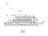
- FIG. 3 is a cross-sectional view of a prior-art mounted LCoS panel 300 that includes LCoS panel 200 electrically connected to a flexible printed circuit assembly (FPCA) 302 .
- FPCA 302 includes a surface-mount connector (not shown) for mechanical and electrical connection to a printed circuit board.
- the portion of FPCA 302 shown in FIG. 2 is bonded to a rigid substrate 350 , which is formed of metal, for example.
- LCoS panel 200 is electrically connected to FPCA 302 via a plurality of wire bonds 383 , conductive glue 386 , and a soldering layer 388 .
- Conductive glue 386 has a height 386 H.
- Encapsulation glue 391 covers wire bonds 383 .
- Soldering layer 388 and conductive glue 386 electrically connect transparent conductive layer 218 to a conductive pad 304 of FPCA 302 , which is connected to a conductive pad trace 306 of FPCA 302 .
- Each of a plurality of address electrodes 305 of FPCA 302 receives a signal from a respective one of a plurality of address electrode traces 303 of FPCA 302 .
- Each wire bond 383 carries a signal from a respective address electrode 305 to a respective bond pad 287 .
- Address electrodes 305 , wire bonds 383 , and bond pads 287 are arranged in respective one-dimensional arrays into the plane of FIG. 3 such that each address electrode 305 is substantially aligned with a respective bond pad 287 .
- the present invention address two suboptimal features of prior-art mounted LCoS panel 300 .
- the first suboptimal feature is that encapsulation glue 391 provides only limited protection to wire bonds 383 , such that wire bonds 383 remain vulnerable to damage.
- the second suboptimal feature arises from height 386 H of conductive glue 386 , which approximately 0.7 mm. The required amount of conductive glue 386 makes its per-volume cost a nontrivial issue and increases risk of conductivity failure between conductive pad 304 and soldering layer 388 .
- a panel carrier for an LCoS panel includes a substrate, a die-attach region, a short sidewall, and a conductor.
- the substrate has a top substrate surface.
- the die-attach region is on the top substrate surface for supporting the LCoS panel.
- the short sidewall is on a first side of the die-attach region and has (i) a top sidewall surface at a first height above the top substrate surface exceeding 0.4 millimeters, and (ii) an aperture spanning the top sidewall surface and the top substrate surface.
- the conductor at least partially fills the aperture for electrically connecting to a conductive layer of the LCoS panel.
- a panel carrier for the LCoS panel includes the substrate, the die-attach region, a short sidewall, the conductor, and a plurality of bond-pad electrodes.
- the tall sidewall extends to a first height above the top substrate surface, exceeding one millimeter, for protecting electrical connections to the plurality of bond-pad electrodes, which are located between the tall sidewall and the die-attach region.
- the plurality of bond-pad electrodes is exposed on the top substrate surface and located between the die-attach region and the tall sidewall. Each bond-pad electrode corresponds to a respective one of the plurality of bond pads.
- a method for mechanically and electrically connecting an LCoS panel to a panel carrier having a short sidewall includes a step of electrically connecting a transparent conductive layer of the LCoS panel to a conductive material, within the short sidewall, with a conductive adhesive having a thickness, between the transparent conductive layer and the short sidewall, less than two-hundred micrometers.
- FIG. 1 shows a prior art LCoS panel on a printed circuit board (PCB) incorporated into a near-eye display attached to a pair of eyeglasses.
- PCB printed circuit board
- FIG. 2 is a perspective view of the prior-art LCoS panel of FIG. 1 .
- FIG. 3 is a cross-sectional view of a prior-art LCoS panel module.
- FIG. 4 is an isometric view of a panel carrier, in an embodiment.
- FIG. 5 is a cross-sectional view of panel carrier of FIG. 4 with the LCoS panel of FIG. 2 therein, in an embodiment.
- FIG. 6 is a flowchart illustrating a method for mechanically and electrically connecting an LCoS panel to a panel carrier, in an embodiment.
- FIG. 4 is an isometric view of a panel carrier 400 .
- Panel carrier 400 includes a substrate 410 that has a top surface 410 T opposite a bottom surface 410 B. Both surfaces 410 T and 410 B are in respective planes parallel to the x-y plane of a coordinate system 498 .
- Top surface 410 T includes a first region 410 T( 1 ) and a second region 410 T( 2 ).
- Panel carrier 400 includes at least one of a short sidewall 420 , on first region 410 T( 1 ), and a tall sidewall 430 on first region 410 T( 2 ).
- Panel carrier 400 includes both short sidewall 420 and tall sidewall 430 in the following description.
- Top surface 410 T that includes a plurality of bond-pad electrodes 414 formed thereon. Top surface 410 T also includes a die-attach region 412 between bond-pad electrodes 414 and first region 410 T( 1 ).
- Short sidewall 420 has a top surface 420 T.
- Sidewall 420 and 430 has heights 420 H, which is for example 0.6 ⁇ 0.2 mm.
- Surface 420 T may be in a plane parallel to the x-y plane of coordinate system 498 .
- Tall sidewall 430 has a height 430 H, which is for example 1.5 ⁇ 0.2 mm.
- Substrate 410 and at least one of sidewall 420 and sidewall 430 may be monolithic. Alternatively, substrate 410 , sidewall 420 , and sidewall 430 may be formed of respective pieces bonded together. Substrate 410 and sidewalls 420 and 430 are formed of a ceramic material such as aluminum oxide (Al 2 O 3 ) or aluminum nitride (AlN). Ceramic materials have physical properties, such as thermal conductivity, thermal expansion coefficient and flexural strength, that make them appropriate for microelectronics packaging applications such as the panel carrier discussed herein.
- Al 2 O 3 aluminum oxide
- AlN aluminum nitride
- Sidewall 420 has an aperture 422 extending between top surface 420 T through a bottom surface of sidewall 420 opposite top surface 420 T.
- Aperture 422 is at least partially filled with a conductor 424 , which may be formed of aluminum, copper, tungsten, or other conductors suitable for electrical connection between layers.
- Conductor 424 may be electrically connected to a conductor having an exposed surface on substrate 410 .
- conductor 424 is electrically connected to a conductive pad on top surface 410 T, which is electrically connected to a conductor exposed on at least one of bottom surface 410 B and a side surface 410 S of substrate 410 .
- Sidewall 420 may also include a conductive pad 428 at least partially covering aperture 422 and electrically connected to conductor 424 .
- Substrate 410 may include an aperture between its surfaces 410 T and 410 B that is aligned with aperture 422 .
- conductor 424 may extend through both sidewall 420 and substrate 410 .
- aperture 422 may extend through both sidewall 420 and substrate 410 .
- Aperture 422 occupies regions 426 X and 426 Y in sidewall 420 .
- sidewall 420 may include a plurality of apertures 423 , within regions 426 X and 426 Y, each at least partially filled with a conductive material similar to conductor 424 .
- Each aperture 423 has, for example, a diameter of at least one hundred micrometers.
- Conductive material in an aperture 423 may have thickness of 10 ⁇ 3 micrometers.
- FIG. 5 is a cross-sectional view of panel carrier 400 with LCoS panel 200 therein, which together form an LCoS device 500 .
- the cross-sectional view of FIG. 5 is parallel to the x-z plane of coordinate system 498 .
- Wafer 214 of LCoS panel 200 is disposed on die-attach region 412 , which may include a die-attach film between surfaces 410 T and 214 B.
- Sidewalls 420 and 430 have respective inner surfaces 420 S and 430 S.
- LCoS device 500 may include bonding wires 583 the electrically connect each bond-pad electrode 414 to a respective bond pad 287 .
- Conductive layer 218 and conductive pad 428 are separated by a distance ⁇ z 1 .
- the top surface of conductive pad 428 may be flush with top surface 420 T. Absent conductive pad 428 , distance ⁇ z 1 is the distance between conductive layer 217 and top surface 420 T.
- LCoS device 500 may also include conductive adhesive 586 spanning distance ⁇ z 1 between conductive layer 218 and conductive pad 428 .
- Conductive adhesive 586 is for example conductive glue.
- Wafer 214 has a nominal height 214 H, which has a tolerance ⁇ z 2 . Height 214 H is for example 0.775 millimeters, and tolerance ⁇ z 2 is for example 0.1 millimeters.
- Height 420 H is less than height 214 H by at least ⁇ z 2 , such that distance ⁇ z 1 is positive to accommodate conductive adhesive 586 .
- 100 ⁇ m ⁇ z 1 ⁇ 200 ⁇ m which accommodates a sufficient thickness of conductive adhesive 586 for proper functionality while limiting cost of the conductive adhesive compared to prior-art mounted LCoS panel 300 .
- Sidewall 430 protects bonding wires 583 , for example, from incidental contact with an object that, absent sidewall 430 , would exerting a force F 1 on one or more bonding wires 583 .
- height 430 H of tall sidewall 430 exceeds a height 200 H of LCoS panel 200 , which provides additional protection to bonding wires 583 .
- LCoS device 500 may also include encapsulation glue 585 on bonding wires 583 .
- FIG. 5 denotes horizontal distances X 1 , X 2 , X 3 , and X 4 .
- Distances X 1 and X 2 may be at least 1.4 mm 0.8 mm, respectively, to accommodate bonding wire 583 , bond-pad electrode 414 , and to enable associated wire bonding processes.
- Sidewall 430 and its distance X 1 from wafer 214 at least partially obviates the need for encapsulation glue 585 .
- Distance X 3 may be at least 0.1 mm, which corresponds to the typical accuracy of a pick-and-place process for placing LCoS panel 200 on panel carrier 400 .
- Distance X 4 may be at least 0.8 mm, which enables adequate electrical connection of conductive layer 218 to conductive pad 428 via conductive adhesive 586 .
- FIG. 6 is a flowchart illustrating a method 600 for mechanically and electrically connecting an LCoS panel to a panel carrier having a short sidewall.
- Step 610 is optional.
- method 600 disposes die-attach film on a top substrate surface adjacent to a short sidewall formed on the top surface.
- a die-attach film is disposed on die-attach region 412 of panel carrier 400 .
- Step 620 is optional.
- method 600 bonds a bottom surface of a semiconductor wafer of an LCoS panel on the die-attach film such that part of a conductive layer of the LCoS panel is directly above the short sidewall.
- bottom surface 214 B is bonded to a die-attach film on surface 410 T of substrate 410 .
- step 630 method 600 electrically connects a conductive layer of the LCoS panel to a conductive material within the short sidewall with a conductive adhesive having a thickness, between the conductive layer and the short sidewall, less than two-hundred micrometers.
- conductive layer 218 of LCoS panel 200 is electrically connected to conductor 424 within short sidewall 420 with conductive adhesive 586 .
- Step 630 may include step 632 , in which method 600 sprays the conductive adhesive on at least one of a top surface of the short sidewall and a surface of the conductive layer facing the short sidewall.
- conductive adhesive 586 is sprayed on top surface 420 T of short sidewall 420 .
- Step 630 may include step 634 , in which the conductive adhesive is a conductive film, such as an anisotropic conductive film.
- the conductive adhesive is a conductive film, such as an anisotropic conductive film.
- method 600 disposes the conductive film on at least one of a top surface of the short sidewall and a surface of the conductive layer facing the short sidewall.
- conductive adhesive 586 is a conductive film disposed as a thin film on top surface 420 T of short sidewall 420 .
- Step 640 is optional, and may be performed when the substrate includes a tall sidewall opposite the short sidewall.
- method 600 wire bonds each one of plurality of bond pads of the LCoS panel to a respective one of a plurality of bond-pad electrodes between the tall sidewall and the die-attach film.
- each bond pad 287 FIGS. 2, 5
- each bond pad 414 FIGS. 4, 5 ).
- a panel carrier includes a substrate, a die-attach region, a short sidewall, and a conductor.
- the substrate has a top substrate surface.
- the die-attach region is on the top substrate surface for supporting the LCoS panel.
- the short sidewall is on a first side of the die-attach region and has (i) a top sidewall surface at a first height above the top substrate surface exceeding 0.4 millimeters, and (ii) an aperture spanning the top sidewall surface and the top substrate surface.
- the conductor at least partially fills the aperture for electrically connecting to a conductive layer of the LCoS panel.
- the panel carrier denoted by (A1) in which the LCoS panel has semiconductor wafer with a plurality of bond pads thereon, may further include a plurality of bond-pad electrodes and a tall sidewall.
- the plurality of bond-pad electrodes are exposed on the top substrate surface, on a side of the die-attach region opposite the short sidewall.
- Each bond-pad electrode corresponds to a respective one of the plurality of bond pads.
- the tall sidewall extends to a second height, above the top substrate surface, exceeding the first height, for protecting electrical connections to the plurality of bond-pad electrodes, which are located between the tall sidewall and the die-attach region.
- the die-attach region is between the tall sidewall and the short sidewall.
- a distance between the tall sidewall and the plurality of bond-pad electrodes may be less than 1.6 millimeters.
- Any panel carrier denoted by one of (A2) and (A3) may further include the LCoS panel, a semiconductor wafer thereof being disposed on the die-attach region.
- the first height is less than a thickness of the semiconductor wafer, and the second height exceeds a total thickness of the LCoS panel.
- the second height may be at least 1.5 millimeters such that it exceeds a total thickness of the LCoS panel.
- Any panel carrier denoted by one of (A2) through (A5) may further include, on the top sidewall surface, a conductive pad electrically connected to the conductor.
- the first height may be less than 0.8 millimeters such that it is less than a thickness of a semiconductor wafer of the LCoS panel.
- a panel carrier for an LCoS panel has the LCoS panel includes a semiconductor wafer with a plurality of bond pads thereon.
- the panel carrier includes a substrate, a die-attach region, a tall sidewall, the conductor, and a plurality of bond-pad electrodes.
- the substrate has a top substrate surface.
- the die-attach region is on the top substrate surface for supporting the LCoS panel.
- the tall sidewall extends to a first height above the top substrate surface, exceeding one millimeter, for protecting electrical connections to the plurality of bond-pad electrodes, which are located between the tall sidewall and the die-attach region.
- the plurality of bond-pad electrodes is exposed on the top substrate surface and located between the die-attach region and the tall sidewall. Each bond-pad electrode corresponds to a respective one of the plurality of bond pads.
- the panel carrier denoted by (B1) may further include a short sidewall and a conductor.
- the short sidewall has (i) a top sidewall surface at a second height above the top substrate surface exceeding 0.4 millimeters, and (ii) an aperture spanning the top sidewall surface and the top substrate surface.
- the conductor at least partially fills the aperture for electrically connecting to a conductive layer of the LCoS panel.
- the die-attach region is between the tall sidewall and the short sidewall.
- the panel carrier denoted by (B2) may further include, on the top sidewall surface, a conductive pad electrically connected to the conductor.
- the second height may be less than 0.8 millimeters such that it is less than a thickness of the semiconductor wafer.
- the first height may be at least 1.5 millimeters such that it exceeds a total thickness of the LCoS panel.
- a distance between the tall sidewall and the plurality of bond-pad electrodes may be less than 1.6 millimeters.
- Any panel carrier denoted by one of (B1) through (B6) may further include the LCoS panel, the semiconductor wafer being disposed on the die-attach region, the first height exceeding a total thickness of the LCoS panel.
- a method for mechanically and electrically connecting a LCoS panel to a panel carrier having a short sidewall includes a step of electrically connecting a transparent conductive layer of the LCoS panel to a conductive material, within the short sidewall, with a conductive adhesive having a thickness less than two-hundred micrometers. The thickness is between the transparent conductive layer and the short sidewall.
- the step of electrically connecting may include spraying the conductive adhesive on at least one of a top surface of the short sidewall and a surface of the transparent conductive layer facing the short sidewall.
- the step of electrically connecting may include disposing the conductive film on at least one of a top surface of the short sidewall and a surface of the transparent conductive layer facing the short sidewall.
Landscapes
- Physics & Mathematics (AREA)
- Nonlinear Science (AREA)
- Mathematical Physics (AREA)
- Chemical & Material Sciences (AREA)
- Crystallography & Structural Chemistry (AREA)
- General Physics & Mathematics (AREA)
- Optics & Photonics (AREA)
- Engineering & Computer Science (AREA)
- Microelectronics & Electronic Packaging (AREA)
- Devices For Indicating Variable Information By Combining Individual Elements (AREA)
- Wire Bonding (AREA)
Abstract
A panel carrier includes a substrate, a die-attach region, a short sidewall, and a conductor. The die-attach region is on a top substrate surface of the substrate for supporting the LCoS panel. The short sidewall is on a first side of the die-attach region and has a top sidewall surface at a first height above the top substrate surface exceeding 0.4 millimeters and an aperture spanning the top sidewall surface and the top substrate surface. The conductor at least partially fills the aperture for electrically connecting to the conductive layer. A method for mechanically and electrically connecting a LCoS panel to a panel carrier having a short sidewall includes electrically connecting a transparent conductive layer of the LCoS panel to a conductive material, within the short sidewall, with a conductive adhesive having a thickness, between the transparent conductive layer and the short sidewall, less than two-hundred micrometers.
Description
Liquid-crystal-on-silicon (LCoS) displays are used in consumer electronics, such as hand-held projectors and near-eye displays. FIG. 1 shows one exemplary use scenario for a prior art LCoS panel 200, wherein LCoS panel 200 is located on a PCB 102 incorporated into a near-eye display 130 attached to eyeglasses 120. LCoS panel 200 may alternately be employed in a different display device, such as in a hand-held image projector.
A transparent conductive layer 218 is on the surface of cover glass 219 adjacent to liquid crystal layer 217. For clarity of illustration, FIG. 2 shows only a portion of conductive layer 218 on overhang region 229 of cover glass 219. Dam 216 contains liquid crystal layer 217. Semiconductor wafer 214 is formed of silicon, for example. Transparent conductive layer 218 is deposited on cover glass 219, and is, for example, formed of indium titanium oxide (ITO). LCoS panel 200 has a panel width 222 and a panel depth 223.
The present invention address two suboptimal features of prior-art mounted LCoS panel 300. The first suboptimal feature is that encapsulation glue 391 provides only limited protection to wire bonds 383, such that wire bonds 383 remain vulnerable to damage. The second suboptimal feature arises from height 386H of conductive glue 386, which approximately 0.7 mm. The required amount of conductive glue 386 makes its per-volume cost a nontrivial issue and increases risk of conductivity failure between conductive pad 304 and soldering layer 388.
In one embodiment, a panel carrier for an LCoS panel is disclosed. The panel carrier includes a substrate, a die-attach region, a short sidewall, and a conductor. The substrate has a top substrate surface. The die-attach region is on the top substrate surface for supporting the LCoS panel. The short sidewall is on a first side of the die-attach region and has (i) a top sidewall surface at a first height above the top substrate surface exceeding 0.4 millimeters, and (ii) an aperture spanning the top sidewall surface and the top substrate surface. The conductor at least partially fills the aperture for electrically connecting to a conductive layer of the LCoS panel.
In another embodiment, a panel carrier for the LCoS panel is disclosed. The panel carrier includes the substrate, the die-attach region, a short sidewall, the conductor, and a plurality of bond-pad electrodes. The tall sidewall extends to a first height above the top substrate surface, exceeding one millimeter, for protecting electrical connections to the plurality of bond-pad electrodes, which are located between the tall sidewall and the die-attach region. The plurality of bond-pad electrodes is exposed on the top substrate surface and located between the die-attach region and the tall sidewall. Each bond-pad electrode corresponds to a respective one of the plurality of bond pads.
In another embodiment, a method for mechanically and electrically connecting an LCoS panel to a panel carrier having a short sidewall is disclosed. The method includes a step of electrically connecting a transparent conductive layer of the LCoS panel to a conductive material, within the short sidewall, with a conductive adhesive having a thickness, between the transparent conductive layer and the short sidewall, less than two-hundred micrometers.
Distance X3 may be at least 0.1 mm, which corresponds to the typical accuracy of a pick-and-place process for placing LCoS panel 200 on panel carrier 400. Distance X4 may be at least 0.8 mm, which enables adequate electrical connection of conductive layer 218 to conductive pad 428 via conductive adhesive 586.
Step 620 is optional. In step 620, method 600 bonds a bottom surface of a semiconductor wafer of an LCoS panel on the die-attach film such that part of a conductive layer of the LCoS panel is directly above the short sidewall. In an example of step 620, bottom surface 214B is bonded to a die-attach film on surface 410T of substrate 410.
In step 630, method 600 electrically connects a conductive layer of the LCoS panel to a conductive material within the short sidewall with a conductive adhesive having a thickness, between the conductive layer and the short sidewall, less than two-hundred micrometers. In an example of step 630, conductive layer 218 of LCoS panel 200 is electrically connected to conductor 424 within short sidewall 420 with conductive adhesive 586.
Step 630 may include step 632, in which method 600 sprays the conductive adhesive on at least one of a top surface of the short sidewall and a surface of the conductive layer facing the short sidewall. In an example of step 632, conductive adhesive 586 is sprayed on top surface 420T of short sidewall 420.
Step 630 may include step 634, in which the conductive adhesive is a conductive film, such as an anisotropic conductive film. In step 634, method 600 disposes the conductive film on at least one of a top surface of the short sidewall and a surface of the conductive layer facing the short sidewall. In an example of step 632, conductive adhesive 586 is a conductive film disposed as a thin film on top surface 420T of short sidewall 420.
Step 640 is optional, and may be performed when the substrate includes a tall sidewall opposite the short sidewall. In step 640, method 600 wire bonds each one of plurality of bond pads of the LCoS panel to a respective one of a plurality of bond-pad electrodes between the tall sidewall and the die-attach film. In an example of step 640, each bond pad 287 (FIGS. 2, 5 ) is wire bonded to a respective bond-pad electrode 414 (FIGS. 4, 5 ).
Combinations of Features.
Features described above as well as those claimed below may be combined in various ways without departing from the scope hereof. The following examples illustrate some possible, non-limiting combinations:
(A1) A panel carrier includes a substrate, a die-attach region, a short sidewall, and a conductor. The substrate has a top substrate surface. The die-attach region is on the top substrate surface for supporting the LCoS panel. The short sidewall is on a first side of the die-attach region and has (i) a top sidewall surface at a first height above the top substrate surface exceeding 0.4 millimeters, and (ii) an aperture spanning the top sidewall surface and the top substrate surface. The conductor at least partially fills the aperture for electrically connecting to a conductive layer of the LCoS panel.
(A2) The panel carrier denoted by (A1), in which the LCoS panel has semiconductor wafer with a plurality of bond pads thereon, may further include a plurality of bond-pad electrodes and a tall sidewall. The plurality of bond-pad electrodes are exposed on the top substrate surface, on a side of the die-attach region opposite the short sidewall. Each bond-pad electrode corresponds to a respective one of the plurality of bond pads. The tall sidewall extends to a second height, above the top substrate surface, exceeding the first height, for protecting electrical connections to the plurality of bond-pad electrodes, which are located between the tall sidewall and the die-attach region. The die-attach region is between the tall sidewall and the short sidewall.
(A3) In the panel carrier denoted by (A2), a distance between the tall sidewall and the plurality of bond-pad electrodes may be less than 1.6 millimeters.
(A4) Any panel carrier denoted by one of (A2) and (A3) may further include the LCoS panel, a semiconductor wafer thereof being disposed on the die-attach region. The first height is less than a thickness of the semiconductor wafer, and the second height exceeds a total thickness of the LCoS panel.
(A5) In any panel carrier denoted by one of (A2) through (A4), the second height may be at least 1.5 millimeters such that it exceeds a total thickness of the LCoS panel.
(A6) Any panel carrier denoted by one of (A2) through (A5) may further include, on the top sidewall surface, a conductive pad electrically connected to the conductor.
(A7) In any panel carrier denoted by one of (A1) through (A6), the first height may be less than 0.8 millimeters such that it is less than a thickness of a semiconductor wafer of the LCoS panel.
(B1) A panel carrier for an LCoS panel is disclosed. The LCoS panel has the LCoS panel includes a semiconductor wafer with a plurality of bond pads thereon. The panel carrier includes a substrate, a die-attach region, a tall sidewall, the conductor, and a plurality of bond-pad electrodes. The substrate has a top substrate surface. The die-attach region is on the top substrate surface for supporting the LCoS panel. The tall sidewall extends to a first height above the top substrate surface, exceeding one millimeter, for protecting electrical connections to the plurality of bond-pad electrodes, which are located between the tall sidewall and the die-attach region. The plurality of bond-pad electrodes is exposed on the top substrate surface and located between the die-attach region and the tall sidewall. Each bond-pad electrode corresponds to a respective one of the plurality of bond pads.
(B2) The panel carrier denoted by (B1) may further include a short sidewall and a conductor. The short sidewall has (i) a top sidewall surface at a second height above the top substrate surface exceeding 0.4 millimeters, and (ii) an aperture spanning the top sidewall surface and the top substrate surface. The conductor at least partially fills the aperture for electrically connecting to a conductive layer of the LCoS panel. The die-attach region is between the tall sidewall and the short sidewall.
(B3) The panel carrier denoted by (B2) may further include, on the top sidewall surface, a conductive pad electrically connected to the conductor.
(B4) In any panel carrier denoted by one of (B2) and (B3), the second height may be less than 0.8 millimeters such that it is less than a thickness of the semiconductor wafer.
(B5) In any panel carrier denoted by one of (B1) through (B4), the first height may be at least 1.5 millimeters such that it exceeds a total thickness of the LCoS panel.
(B6) In any panel carrier denoted by one of (B1) through (B5), a distance between the tall sidewall and the plurality of bond-pad electrodes may be less than 1.6 millimeters.
(B7) Any panel carrier denoted by one of (B1) through (B6) may further include the LCoS panel, the semiconductor wafer being disposed on the die-attach region, the first height exceeding a total thickness of the LCoS panel.
(C1) A method for mechanically and electrically connecting a LCoS panel to a panel carrier having a short sidewall includes a step of electrically connecting a transparent conductive layer of the LCoS panel to a conductive material, within the short sidewall, with a conductive adhesive having a thickness less than two-hundred micrometers. The thickness is between the transparent conductive layer and the short sidewall.
(C2) In the method denoted by (C1), the step of electrically connecting may include spraying the conductive adhesive on at least one of a top surface of the short sidewall and a surface of the transparent conductive layer facing the short sidewall.
(C3) In any method denoted by one of (C1) and (C2), the step of electrically connecting may include disposing the conductive film on at least one of a top surface of the short sidewall and a surface of the transparent conductive layer facing the short sidewall.
Changes may be made in the above methods and systems without departing from the scope hereof. It should thus be noted that the matter contained in the above description or shown in the accompanying drawings should be interpreted as illustrative and not in a limiting sense. The following claims are intended to cover all generic and specific features described herein, as well as all statements of the scope of the present method and system, which, as a matter of language, might be said to fall therebetween.
Claims (12)
1. A panel carrier for a liquid-crystal-on-silicon (LCoS) panel comprising:
a substrate having a top substrate surface;
a die-attach region on the top substrate surface for supporting the LCoS panel;
a first sidewall, on a first side of the die-attach region, having (i) a top sidewall surface at a first height above the top substrate surface exceeding 0.4 millimeters, and (ii) an aperture spanning the top sidewall surface and the top substrate surface; and
a conductor at least partially filling the aperture for electrically connecting to a conductive layer of the LCoS panel.
2. The panel carrier of claim 1 , the LCoS panel having semiconductor wafer with a plurality of bond pads thereon, further comprising:
a plurality of bond-pad electrodes exposed on the top substrate surface, on a side of the die-attach region opposite the first sidewall, each bond-pad electrode corresponding to a respective one of the plurality of bond pads;
a second sidewall extending to a second height, above the top substrate surface, exceeding the first height, for protecting electrical connections to the plurality of bond-pad electrodes, which are located between the second sidewall and the die-attach region,
the die-attach region being between the second sidewall and the first sidewall.
3. The panel carrier of claim 2 , a distance between the second sidewall and the plurality of bond-pad electrodes being less than 1.6 millimeters.
4. The panel carrier of claim 2 , further comprising the LCoS panel, a semiconductor wafer thereof being disposed on the die-attach region, the first height being less than a thickness of the semiconductor wafer, and the second height exceeding a total thickness of the LCoS panel.
5. The panel carrier of claim 2 , the second height being at least 1.5 millimeters such that it exceeds a total thickness of the LCoS panel.
6. The panel carrier of claim 1 , further comprising, on the top sidewall surface, a conductive pad electrically connected to the conductor.
7. The panel carrier of claim 1 , the first height being less than 0.8 millimeters such that it is less than a thickness of a semiconductor wafer of the LCoS panel.
8. The panel carrier of claim 1 , the first sidewall being formed entirely of a ceramic material.
9. A method for mechanically and electrically connecting a liquid-crystal-on-silicon (LCoS) panel to a panel carrier, the method comprising: electrically connecting a transparent conductive layer of the LCoS panel to a conductive material, within an aperture through a first sidewall of the LCoS panel carrier, with a conductive adhesive having a thickness, between the transparent conductive layer and the first sidewall, less than two-hundred micrometers.
10. The method of claim 9 , the step of electrically connecting comprising:
spraying the conductive adhesive on at least one of a top surface of the first sidewall and a surface of the transparent conductive layer facing the first sidewall.
11. The method of claim 9 , the conductive adhesive being a conductive film, the step of electrically connecting comprising:
disposing the conductive film on at least one of a top surface of the first sidewall and a surface of the transparent conductive layer facing the first sidewall.
12. The method of claim 9 , the first sidewall being formed entirely of a ceramic material.
Priority Applications (1)
| Application Number | Priority Date | Filing Date | Title |
|---|---|---|---|
| US15/226,731 US10185191B2 (en) | 2016-08-02 | 2016-08-02 | Panel carrier and method for attaching a liquid-crystal-on-silicon panel thereto |
Applications Claiming Priority (1)
| Application Number | Priority Date | Filing Date | Title |
|---|---|---|---|
| US15/226,731 US10185191B2 (en) | 2016-08-02 | 2016-08-02 | Panel carrier and method for attaching a liquid-crystal-on-silicon panel thereto |
Publications (2)
| Publication Number | Publication Date |
|---|---|
| US20180039126A1 US20180039126A1 (en) | 2018-02-08 |
| US10185191B2 true US10185191B2 (en) | 2019-01-22 |
Family
ID=61069174
Family Applications (1)
| Application Number | Title | Priority Date | Filing Date |
|---|---|---|---|
| US15/226,731 Active US10185191B2 (en) | 2016-08-02 | 2016-08-02 | Panel carrier and method for attaching a liquid-crystal-on-silicon panel thereto |
Country Status (1)
| Country | Link |
|---|---|
| US (1) | US10185191B2 (en) |
Citations (19)
| Publication number | Priority date | Publication date | Assignee | Title |
|---|---|---|---|---|
| US4942076A (en) | 1988-11-03 | 1990-07-17 | Micro Substrates, Inc. | Ceramic substrate with metal filled via holes for hybrid microcircuits and method of making the same |
| US6120708A (en) | 1998-03-25 | 2000-09-19 | Murata Manufacturing Co., Ltd. | Conductive paste and method for producing ceramic substrate using the same |
| WO2001077747A2 (en) | 2000-04-05 | 2001-10-18 | Digital Reflection, Inc. | Reflective microdisplay for light engine based video projection applications |
| US6356334B1 (en) | 1998-08-06 | 2002-03-12 | National Semiconductor Corporation | Liquid crystal display assembly and method for reducing residual stresses |
| US20020071085A1 (en) | 2000-12-08 | 2002-06-13 | Industrial Technology Research Institute | Method for interconnecting a flat panel display having a non-transparent substrate and devices formed |
| US20020085158A1 (en) | 1999-05-17 | 2002-07-04 | Karl M. Armagost | Ball grid array mounted liquid crystal display panels |
| US6897933B2 (en) | 2001-03-14 | 2005-05-24 | Seiko Epson Corporation | Substrate terminal structure, liquid-crystal device and electronic apparatus |
| US20060072063A1 (en) * | 2004-10-05 | 2006-04-06 | Gihong Kim | Carbon nano tube technology in liquid crystal on silicon micro-display |
| US7786747B2 (en) | 2007-11-30 | 2010-08-31 | Texas Instruments Incorporated | Microdisplay assemblies and methods of packaging microdisplays |
| US7808573B2 (en) | 2008-08-14 | 2010-10-05 | Himax Display, Inc. | Display (LCOS) panel module having an adhesive on a subtrate with a flexible printed circuit (FPC) having an opening so that the LCOS panel may be adhesively connected to the substrate and electrically connected to the FPC through the opening |
| US20100328590A1 (en) | 2009-06-29 | 2010-12-30 | Jiangsu Lexvu Electronics Co., Ltd. | Back substrate and reflective liquid crystal display |
| JP2012013975A (en) * | 2010-07-01 | 2012-01-19 | Citizen Finetech Miyota Co Ltd | Liquid crystal display element |
| US8339563B2 (en) | 2009-09-21 | 2012-12-25 | Shanghai Lexvu Opto Microelectronics Technology Co., Ltd | Liquid crystal imager and method of making same |
| US20130242244A1 (en) * | 2012-03-19 | 2013-09-19 | Frank Supon | Methods and apparatus for electrically connecting a substrate and electrically conductive glass |
| US20130242243A1 (en) * | 2012-03-16 | 2013-09-19 | Frank Supon | Methods and apparatus for connecting electrically conductive glass to a substrate in a liquid crystal panel |
| US20130320557A1 (en) | 2012-05-31 | 2013-12-05 | Hon Hai Precision Industry Co., Ltd. | Semiconductor package having reliable electrical connection and assembling method |
| US20130333744A1 (en) * | 2011-01-27 | 2013-12-19 | Hitachi Chemical Company, Ltd. | Conductive binder composition, metal wire with conductive binder, bonded unit, and solar cell module |
| US8680572B2 (en) | 2003-12-31 | 2014-03-25 | Intel Corporation | Microdisplay packaging system |
| US9229280B2 (en) | 2012-09-27 | 2016-01-05 | Omnivision Technologies (Shanghai) Co., Ltd. | LCOS panel and method of manufacturing the same |
-
2016
- 2016-08-02 US US15/226,731 patent/US10185191B2/en active Active
Patent Citations (20)
| Publication number | Priority date | Publication date | Assignee | Title |
|---|---|---|---|---|
| US4942076A (en) | 1988-11-03 | 1990-07-17 | Micro Substrates, Inc. | Ceramic substrate with metal filled via holes for hybrid microcircuits and method of making the same |
| US6120708A (en) | 1998-03-25 | 2000-09-19 | Murata Manufacturing Co., Ltd. | Conductive paste and method for producing ceramic substrate using the same |
| US6356334B1 (en) | 1998-08-06 | 2002-03-12 | National Semiconductor Corporation | Liquid crystal display assembly and method for reducing residual stresses |
| US20020085158A1 (en) | 1999-05-17 | 2002-07-04 | Karl M. Armagost | Ball grid array mounted liquid crystal display panels |
| WO2001077747A2 (en) | 2000-04-05 | 2001-10-18 | Digital Reflection, Inc. | Reflective microdisplay for light engine based video projection applications |
| US20020071085A1 (en) | 2000-12-08 | 2002-06-13 | Industrial Technology Research Institute | Method for interconnecting a flat panel display having a non-transparent substrate and devices formed |
| US6501525B2 (en) | 2000-12-08 | 2002-12-31 | Industrial Technology Research Institute | Method for interconnecting a flat panel display having a non-transparent substrate and devices formed |
| US6897933B2 (en) | 2001-03-14 | 2005-05-24 | Seiko Epson Corporation | Substrate terminal structure, liquid-crystal device and electronic apparatus |
| US8680572B2 (en) | 2003-12-31 | 2014-03-25 | Intel Corporation | Microdisplay packaging system |
| US20060072063A1 (en) * | 2004-10-05 | 2006-04-06 | Gihong Kim | Carbon nano tube technology in liquid crystal on silicon micro-display |
| US7786747B2 (en) | 2007-11-30 | 2010-08-31 | Texas Instruments Incorporated | Microdisplay assemblies and methods of packaging microdisplays |
| US7808573B2 (en) | 2008-08-14 | 2010-10-05 | Himax Display, Inc. | Display (LCOS) panel module having an adhesive on a subtrate with a flexible printed circuit (FPC) having an opening so that the LCOS panel may be adhesively connected to the substrate and electrically connected to the FPC through the opening |
| US20100328590A1 (en) | 2009-06-29 | 2010-12-30 | Jiangsu Lexvu Electronics Co., Ltd. | Back substrate and reflective liquid crystal display |
| US8339563B2 (en) | 2009-09-21 | 2012-12-25 | Shanghai Lexvu Opto Microelectronics Technology Co., Ltd | Liquid crystal imager and method of making same |
| JP2012013975A (en) * | 2010-07-01 | 2012-01-19 | Citizen Finetech Miyota Co Ltd | Liquid crystal display element |
| US20130333744A1 (en) * | 2011-01-27 | 2013-12-19 | Hitachi Chemical Company, Ltd. | Conductive binder composition, metal wire with conductive binder, bonded unit, and solar cell module |
| US20130242243A1 (en) * | 2012-03-16 | 2013-09-19 | Frank Supon | Methods and apparatus for connecting electrically conductive glass to a substrate in a liquid crystal panel |
| US20130242244A1 (en) * | 2012-03-19 | 2013-09-19 | Frank Supon | Methods and apparatus for electrically connecting a substrate and electrically conductive glass |
| US20130320557A1 (en) | 2012-05-31 | 2013-12-05 | Hon Hai Precision Industry Co., Ltd. | Semiconductor package having reliable electrical connection and assembling method |
| US9229280B2 (en) | 2012-09-27 | 2016-01-05 | Omnivision Technologies (Shanghai) Co., Ltd. | LCOS panel and method of manufacturing the same |
Non-Patent Citations (7)
| Title |
|---|
| "Semiconductor manufacturing techniques for ferroelectric liquid crystal microdisplays," Laser Focus World http://www.laserfocusworld.com/articles/print/volume-36/issue-5/features/flat-panel-displays/semiconductor-manufacturing-techniques-for-ferroelectric-liquid-crystal-microdisplays.html. |
| Bleha, et al., "Advances in Liquid Crystal on Silicon (LCOS) Spatial Light Modulator Technology," Proc. of SPIE, vol. 8736, 2013. |
| Goldstein, et al., "Packaging of Liquid Crystal on Silicon Microdisplays," website http://electroiq.com/blog/2001/05/packaging-of-liquid-crystal-on-silicon-microdisplays/, 2001. |
| Huang, et al., "Integrated Digital Input Driver for Active Matrix Liquid-Crystal-On-Silicon Display," Department of Electrical and Electronic Engineering, The Hong Kong University of Science of Technology, 1995. |
| Steen, "Design of LCOS Microdisplay Backplanes for Projection Applications," ISBN 90-8578-062-4, Universiteit Gent, 2005-2006. |
| Translation of Taiwanese Office Action corresponding to Taiwanese Patent Application No. 104137949, dated Jun. 27, 2016, 4 pages. |
| Underwood, "A Review of Microdisplay Technologies," the University of Edinburgh, A Keynote Paper presented at the Conference Entitled SID@EID, London, Nov. 21-23, 2000. |
Also Published As
| Publication number | Publication date |
|---|---|
| US20180039126A1 (en) | 2018-02-08 |
Similar Documents
| Publication | Publication Date | Title |
|---|---|---|
| KR100497997B1 (en) | Semiconductor module | |
| US9113545B2 (en) | Tape wiring substrate and chip-on-film package including the same | |
| US6399418B1 (en) | Method for forming a reduced thickness packaged electronic device | |
| CN109698184B (en) | Film for packaging substrate, semiconductor packaging and display devices | |
| US9847282B2 (en) | Semiconductor device | |
| US6586824B1 (en) | Reduced thickness packaged electronic device | |
| US9760754B2 (en) | Printed circuit board assembly forming enhanced fingerprint module | |
| US10720370B2 (en) | Sensor package structure | |
| KR20160092123A (en) | Display apparatus and manufacturing method thereof | |
| CN105826353A (en) | Chip on film and display device | |
| CN114026685B (en) | Electronic devices and their mounting structures | |
| WO2008072551A1 (en) | Ic chip-mounted package and image display device using the same | |
| KR102446203B1 (en) | Driving chip and display device including same | |
| CN109417081B (en) | Chip packaging structure, method and electronic equipment | |
| US9568789B2 (en) | Panel carrier for a liquid crystal on silicon panel and method for electrically interconnecting same | |
| US10614988B2 (en) | Package structure of display panel, connecting board, package method and display device | |
| US10185191B2 (en) | Panel carrier and method for attaching a liquid-crystal-on-silicon panel thereto | |
| US20100181636A1 (en) | Optical device, solid-state imaging device, and method of manufacturing optical device | |
| US12470200B2 (en) | Electronic component housing package, electronic device, and electronic module | |
| TWI415227B (en) | Chip package structure and wire structure | |
| CN110518027B (en) | Sensor Package Structure | |
| CN117038683B (en) | Opto-mechanical-electrical module, semiconductor packaging assembly and manufacturing method thereof | |
| KR102917157B1 (en) | Display device | |
| CN210040172U (en) | Chip packaging structure and electronic equipment | |
| KR101004897B1 (en) | Multi Chip Module Package |
Legal Events
| Date | Code | Title | Description |
|---|---|---|---|
| AS | Assignment |
Owner name: OMNIVISION TECHNOLOGIES, INC., CALIFORNIA Free format text: ASSIGNMENT OF ASSIGNORS INTEREST;ASSIGNORS:LI, EN-CHI;HUANG, CHI-CHIH;REEL/FRAME:039320/0352 Effective date: 20160725 |
|
| STCF | Information on status: patent grant |
Free format text: PATENTED CASE |
|
| MAFP | Maintenance fee payment |
Free format text: PAYMENT OF MAINTENANCE FEE, 4TH YEAR, LARGE ENTITY (ORIGINAL EVENT CODE: M1551); ENTITY STATUS OF PATENT OWNER: LARGE ENTITY Year of fee payment: 4 |