US10180216B2 - Light emitting apparatus, back light unit and display apparatus - Google Patents
Light emitting apparatus, back light unit and display apparatus Download PDFInfo
- Publication number
- US10180216B2 US10180216B2 US14/555,893 US201414555893A US10180216B2 US 10180216 B2 US10180216 B2 US 10180216B2 US 201414555893 A US201414555893 A US 201414555893A US 10180216 B2 US10180216 B2 US 10180216B2
- Authority
- US
- United States
- Prior art keywords
- component
- light emitting
- recess
- protrusion
- components
- Prior art date
- Legal status (The legal status is an assumption and is not a legal conclusion. Google has not performed a legal analysis and makes no representation as to the accuracy of the status listed.)
- Expired - Fee Related, expires
Links
Images


Classifications
-
- F—MECHANICAL ENGINEERING; LIGHTING; HEATING; WEAPONS; BLASTING
- F21—LIGHTING
- F21S—NON-PORTABLE LIGHTING DEVICES; SYSTEMS THEREOF; VEHICLE LIGHTING DEVICES SPECIALLY ADAPTED FOR VEHICLE EXTERIORS
- F21S4/00—Lighting devices or systems using a string or strip of light sources
- F21S4/20—Lighting devices or systems using a string or strip of light sources with light sources held by or within elongate supports
- F21S4/28—Lighting devices or systems using a string or strip of light sources with light sources held by or within elongate supports rigid, e.g. LED bars
-
- H—ELECTRICITY
- H01—ELECTRIC ELEMENTS
- H01L—SEMICONDUCTOR DEVICES NOT COVERED BY CLASS H10
- H01L33/00—Semiconductor devices with at least one potential-jump barrier or surface barrier specially adapted for light emission; Processes or apparatus specially adapted for the manufacture or treatment thereof or of parts thereof; Details thereof
- H01L33/48—Semiconductor devices with at least one potential-jump barrier or surface barrier specially adapted for light emission; Processes or apparatus specially adapted for the manufacture or treatment thereof or of parts thereof; Details thereof characterised by the semiconductor body packages
- H01L33/483—Containers
-
- F21S4/008—
-
- G—PHYSICS
- G02—OPTICS
- G02F—OPTICAL DEVICES OR ARRANGEMENTS FOR THE CONTROL OF LIGHT BY MODIFICATION OF THE OPTICAL PROPERTIES OF THE MEDIA OF THE ELEMENTS INVOLVED THEREIN; NON-LINEAR OPTICS; FREQUENCY-CHANGING OF LIGHT; OPTICAL LOGIC ELEMENTS; OPTICAL ANALOGUE/DIGITAL CONVERTERS
- G02F1/00—Devices or arrangements for the control of the intensity, colour, phase, polarisation or direction of light arriving from an independent light source, e.g. switching, gating or modulating; Non-linear optics
- G02F1/01—Devices or arrangements for the control of the intensity, colour, phase, polarisation or direction of light arriving from an independent light source, e.g. switching, gating or modulating; Non-linear optics for the control of the intensity, phase, polarisation or colour
- G02F1/13—Devices or arrangements for the control of the intensity, colour, phase, polarisation or direction of light arriving from an independent light source, e.g. switching, gating or modulating; Non-linear optics for the control of the intensity, phase, polarisation or colour based on liquid crystals, e.g. single liquid crystal display cells
- G02F1/133—Constructional arrangements; Operation of liquid crystal cells; Circuit arrangements
- G02F1/1333—Constructional arrangements; Manufacturing methods
- G02F1/1335—Structural association of cells with optical devices, e.g. polarisers or reflectors
- G02F1/1336—Illuminating devices
- G02F1/133602—Direct backlight
- G02F1/133603—Direct backlight with LEDs
-
- G—PHYSICS
- G02—OPTICS
- G02F—OPTICAL DEVICES OR ARRANGEMENTS FOR THE CONTROL OF LIGHT BY MODIFICATION OF THE OPTICAL PROPERTIES OF THE MEDIA OF THE ELEMENTS INVOLVED THEREIN; NON-LINEAR OPTICS; FREQUENCY-CHANGING OF LIGHT; OPTICAL LOGIC ELEMENTS; OPTICAL ANALOGUE/DIGITAL CONVERTERS
- G02F1/00—Devices or arrangements for the control of the intensity, colour, phase, polarisation or direction of light arriving from an independent light source, e.g. switching, gating or modulating; Non-linear optics
- G02F1/01—Devices or arrangements for the control of the intensity, colour, phase, polarisation or direction of light arriving from an independent light source, e.g. switching, gating or modulating; Non-linear optics for the control of the intensity, phase, polarisation or colour
- G02F1/13—Devices or arrangements for the control of the intensity, colour, phase, polarisation or direction of light arriving from an independent light source, e.g. switching, gating or modulating; Non-linear optics for the control of the intensity, phase, polarisation or colour based on liquid crystals, e.g. single liquid crystal display cells
- G02F1/133—Constructional arrangements; Operation of liquid crystal cells; Circuit arrangements
- G02F1/1333—Constructional arrangements; Manufacturing methods
- G02F1/1335—Structural association of cells with optical devices, e.g. polarisers or reflectors
- G02F1/1336—Illuminating devices
- G02F1/133602—Direct backlight
- G02F1/133608—Direct backlight including particular frames or supporting means
-
- G—PHYSICS
- G02—OPTICS
- G02F—OPTICAL DEVICES OR ARRANGEMENTS FOR THE CONTROL OF LIGHT BY MODIFICATION OF THE OPTICAL PROPERTIES OF THE MEDIA OF THE ELEMENTS INVOLVED THEREIN; NON-LINEAR OPTICS; FREQUENCY-CHANGING OF LIGHT; OPTICAL LOGIC ELEMENTS; OPTICAL ANALOGUE/DIGITAL CONVERTERS
- G02F2201/00—Constructional arrangements not provided for in groups G02F1/00 - G02F7/00
- G02F2201/16—Constructional arrangements not provided for in groups G02F1/00 - G02F7/00 series; tandem
-
- H—ELECTRICITY
- H01—ELECTRIC ELEMENTS
- H01L—SEMICONDUCTOR DEVICES NOT COVERED BY CLASS H10
- H01L33/00—Semiconductor devices with at least one potential-jump barrier or surface barrier specially adapted for light emission; Processes or apparatus specially adapted for the manufacture or treatment thereof or of parts thereof; Details thereof
- H01L33/48—Semiconductor devices with at least one potential-jump barrier or surface barrier specially adapted for light emission; Processes or apparatus specially adapted for the manufacture or treatment thereof or of parts thereof; Details thereof characterised by the semiconductor body packages
- H01L33/62—Arrangements for conducting electric current to or from the semiconductor body, e.g. lead-frames, wire-bonds or solder balls
Definitions
- This disclosure relates to a light emitting apparatus, more specifically, a light emitting apparatus that can be applied to a back light unit of a display apparatus.
- a display apparatus such as liquid crystal display (LCD), organic light emitting diode (OLED) display is one of the most widely used apparatus currently.
- LCD liquid crystal display
- OLED organic light emitting diode
- the existing curved surface display apparatus is mainly achieved by designing the screen of the display apparatus into a curved surface form. Therefore, the design and research on the curved surface display mainly focus on the curved surface design of the screen of the display apparatus.
- due to complexity of technology and relatively low yield the development cost of the curved surface display screen is relatively high, and thus its application is limited.
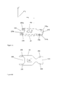
- FIG. 1 shows a light emitting diode (LED) bar in a back light unit of a conventional liquid crystal display.
- the LED bar comprises a plurality of LEDs 101 formed on a common carrier 11 .
- the carrier of such an LED bar uses a metal material as a base material, an insulating layer and a conductor layer are printed on the base material, i.e., fabricating the carrier into a metal core printed circuit board (MCPCB), then welding the LED on the MCPCB.
- MCPCB metal core printed circuit board
- a curved surface liquid crystal display when such an integrated LED bar is used in the back light unit, the LED bar is generally arranged on a non bending side of the display apparatus in order to reduce thickness of the display apparatus, however, this may result in less homogeneity of image luminance of the curved surface display apparatus. Therefore, when such an integrated LED bar is applied to a back light unit of a curved surface display apparatus, the image quality of the curved surface display apparatus will be limited. In addition, failure of one LED in the integrated LED bar may lead to malfunction of the whole LED bar, which causes an inconvenient maintenance of the back light unit and results in a relatively high cost of use of the display apparatus.
- a light emitting apparatus may comprise a middle component, a first end component and a second end component.
- the middle component may comprise a light emitting device and has a recess and a protrusion at its two ends respectively.
- One of the first and second end components has a recess, and the other of the first and second end components has a protrusion.
- the middle component can be connected with the first and the second end components respectively by corresponding protrusion and recess so that adjacent components can rotate relative to each other in a plane perpendicular to a light exit direction of the light emitting device.
- the middle component and the second end component in connection there may be a gap between the recess and the protrusion of the adjacent components.
- the existence of the gap is favorable for heat dissipation of the light emitting apparatus.
- each of the first end component, the middle component and the second end component may comprise an electrode layer, and for the first end component, the middle component and the second end component in connection, the electrode layers of the adjacent components are in electrical contact with each other. Further, the electrode layer of each of the first end component, the middle component and the second end component may extend to an end face of the recess and the protrusion of the component where it locates.
- the number of the middle component comprised by the light emitting apparatus may be more than one, and the middle components can be connected successively by corresponding recesses and protrusions. In this way, light emitting apparatuses of different lengths can be achieved by adjusting the number of the middle components, thereby meeting requirements of different applications.
- each of the recesses and the protrusions of the first and second end components as well as the recess and the protrusion of the middle component may comprise an arcuate portion, and for the first end component, the middle component and the second end component in connection, the arcuate portion of the recess of one component and the arcuate portion of the protrusion of the other component in the adjacent components are in contact with each other.
- each of the recess of the first or the second end components and the recess of the middle component may be a major arc.
- the arcuate portion of each of the protrusion of the first or the second end components and the protrusion of the middle component may also be a major arc.
- the arcuate portion of the recess of one component and the arcuate portion of the protrusion of the other component in the adjacent components have the same radius of curvature.
- At least one of the first end component and the second end component may comprise a connector, and the light emitting device can be powered by an external power supply system via the connector.
- At least one of the first end component and the second end component may comprise a light emitting device.
- the luminance at two ends of the light emitting apparatus can be enhanced.
- the rotation of the adjacent components relative to each other in the plane perpendicular to the light exit direction of the light emitting device enables the light emitting apparatus to bend in the plane, the radius of curvature R of bending is:
- R L 2 ⁇ 1 sin ⁇ ⁇ 4 wherein L is a length of the middle component, ⁇ is a rotation angle of the rotation of the adjacent components relative to each other.
- a back light unit which may comprise a light emitting apparatus according to embodiments of the present invention.
- the curved surface display can be achieved with a relatively low cost and a relatively high yield.
- a display apparatus may comprise a back light unit mentioned above.
- FIG. 1 shows a schematic view of an LED bar in the prior art
- FIG. 2 schematically shows a light emitting apparatus according to an embodiment of the present invention
- FIGS. 3A and 3B schematically show a perspective view and a top view of a first end component of the light emitting apparatus as shown in FIG. 2 respectively;
- FIGS. 4A and 4B schematically show a perspective view and a top view of a middle component of the light emitting apparatus as shown in FIG. 2 respectively;
- FIGS. 5A and 5B schematically show a perspective view and a top view of a second end component of the light emitting apparatus as shown in FIG. 2 respectively;
- FIG. 6 schematically illustrates calculation of radius of curvature of a light emitting apparatus in a bending state according to an embodiment of the present invention
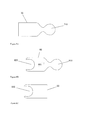
- FIGS. 7A to 7D schematically show a light emitting apparatus according to another embodiment of the present invention.
- FIGS. 8A to 8D schematically show a light emitting apparatus according to a further embodiment of the present invention.
- FIG. 9 shows a schematic view of a light emitting apparatus in a bending state according to an embodiment of the present invention.
- the inventor has recognized that the design and development of the existing curved surface display apparatus mainly focus on design of the screen of the display apparatus into a curved surface form.
- design and development of a curved surface screen may result in complexity of technology and a relatively low yield, and also results in a relatively high cost of development.
- the existing integrated light emitting apparatus e.g. the LED bar ( FIG. 1 )
- the image quality of the curved surface display apparatus will be affected. Therefore, the inventor proposes a modularized and bendable light emitting apparatus.
- the light emitting apparatus for example can be used in a back light unit of a curved surface display apparatus to meet requirement of curved surface display.
- the adjacent components can rotate relative to each other in a plane perpendicular to a light exit direction of the light emitting device, the whole light emitting apparatus can be bended in the plane. Therefore, when such a bendable light emitting apparatus is used in a back light unit of a display apparatus, the curved surface display can be achieved more easily, which improves the yield and will not affect the image quality of the curved surface display apparatus.
- the light emitting apparatus adopts a modularized structure, in the case of malfunction of the light emitting apparatus, it only needs to repair or replace the component where the malfunction occurs rather than replacing the whole light emitting apparatus. In this way, the cost of use and maintenance can be reduced.
- FIG. 2 schematically shows a light emitting apparatus 2 according to an embodiment of the present invention.
- the light emitting apparatus 2 may comprise a first end component 10 , a middle component 20 and a second end component 30 .
- FIG. 2 shows a connection state of the three components in the form of a top view.
- the middle component 20 of the light emitting apparatus 2 may comprise a light emitting device 201 .
- the light emitting device 201 may be any appropriate light emitting device that can serve as a light emitting source, e.g. LED, OLED, bulbs or other point light sources or surface light sources.
- the middle component 20 has a recess 220 and a protrusion 210 at its two ends respectively.
- One of the first end component 10 and the second end component 30 has a recess, the other has a protrusion.
- the first end component 10 has a protrusion 110 at its end
- the second end component 30 has a recess 320 at its end.
- the middle component 20 can be connected with the first end component 10 and the second end component 30 by corresponding protrusions and recesses, so that adjacent components can rotate relative to each other in a plane XY perpendicular to a light exit direction of the light emitting device 201 .
- the middle component 20 can be connected with the first end component 10 by the protrusion 110 and the recess 220 , and the middle component 20 can be connected with the second end component 30 by the protrusion 210 and the recess 320 , so that the adjacent components 10 , 20 can rotate relative to each other in the plane XY perpendicular to the light exit direction of the light emitting device 201 and the adjacent components 20 , 30 can rotate relative to each other in the plane XY perpendicular to the light exit direction of the light emitting device 201 .
- the first end component 10 , the middle component 20 and the second end component 30 in connection there may be a gap between the recess and the protrusion of the adjacent components.
- there may be a gap between the protrusion 110 of the first end component 10 and the recess 220 of the middle component 20 there may be a gap between the protrusion 210 of the middle component 20 and the recess 320 of the second end component 30 .
- the gap between the corresponding protrusion and recess of the adjacent components of the light emitting apparatus 2 may be in any shape, rather than being limited to the gap as shown in FIG. 2 .
- the gap formed by non contact portions of the protrusion 110 of the first end component 10 and the recess 220 of the middle component 20 may be in any irregular shape, as long as it does not affect the rotation of the first end component 10 and the middle component 20 relative to each other in the plane perpendicular to the light exit direction of the light emitting device 201 .
- each of the first end component 10 , the middle component 20 and the second end component 30 of the light emitting apparatus 2 may comprise an electrode, and for the first end component 10 , the middle component 20 and the second end component 30 in connection, the electrode layers of the adjacent components can be in electrical contact with each other.
- the first end component 10 may comprise an electrode 130
- the middle component 20 may comprise an electrode 230
- the second end component 30 may comprise an electrode 330 .
- the electrode of each of the first end component 10 , the middle component 20 and the second end component 30 may extend to an end face of the protrusion and the recess of the component where it locates.
- the electrode 130 may extend to the end face of the protrusion 110 of the first end component 10
- the electrode 230 may extend to the end faces of the recess 220 and the protrusion 210 of the middle component 20
- the electrode 330 may extend to the end face of the recess 320 of the second end component 30 , so that when the first end component 10 , the middle component 20 and the second end component 30 are in connection, they can be electrically connected with one another directly.
- the electrodes 130 , 230 , 330 denoted schematically by broken lines in FIG. 2 only illustrate the portion of electrodes 130 , 230 , 330 that extends to the end faces of the recesses and the protrusions of the first end component 10 , the middle component 20 and the second end component 30 , respectively.
- the electrode layer of each component can be electrically connected with other electrical components included in the first end component 10 , the middle component 20 and the second end component 30 .
- the electrode 230 of the middle component 20 can be electrically connected with the light emitting device 201 , so that the light emitting device 201 can be powered via the electrode 230 to enable the light emitting device 201 to emit light.
- the electrodes shown in FIG. 2 are located at two sides of the corresponding recess or protrusion, this is only an example, rather than limitation to the present invention. In fact, the electrodes may also be located at only one side of the corresponding recess or protrusion.
- the specific shapes of the protrusions and the recesses of the components can be selected based on actual needs, as long as the adjacent components can rotate relative to each other in the plane perpendicular to the light exit direction of the light emitting device after the components are in connection by corresponding protrusions and recesses.
- FIG. 2 shows an example of the specific shapes of the protrusions and the recesses.
- each of the protrusion 110 of the first end component 10 , the recess 320 of the second end component 30 as well as the recess 220 and the protrusion 210 of the middle component 20 may comprise an arcuate portion, and for the first end component 10 , the middle component 20 and the second end component 30 in connection, the arcuate portion of the protrusion 110 of the first end component 10 and the arcuate portion of the recess 220 of the middle component 20 can be in contact with each other, the arcuate portion of the protrusion 210 of the middle component 20 and the arcuate portion of the recess 320 of the second end component 30 can be in contact with each other.
- the protrusion 110 of the first end component 10 and the recess 320 of the second end component 30 as well as the recess 220 and the protrusion 210 of the middle component 20 may comprise an arch portion is only an example, rather than limitation to the present invention.
- the corresponding recesses and protrusions of the first and second end components as well as the middle component may also comprise portions in other forms that can be in contact with the protrusions or the recesses of adjacent components.
- the recesses and protrusions of the corresponding components can also be connected by use of other mechanical connection manners (such as hinge connection) well known by the skilled person in the art, as long as the adjacent components can rotate relative to each other in the plane perpendicular to the light exit direction of the light emitting device.
- other mechanical connection manners such as hinge connection
- sizes of the corresponding protrusions and recesses of the components in the light emitting apparatus can be designed so that the connection of the adjacent components is tighter.
- the sizes of the recess 220 of the middle component 20 and the protrusion 110 of the first end component 10 can be designed such that the distance d 1 at the opening of the recess 220 is smaller than the maximum diameter D 1 of the protrusion 110 .
- the maximum diameter D 1 herein is the maximum distance between outer edges of two sides of the protrusion 110 in Y direction.
- the sizes of the recess 320 of the second end component 30 and the protrusion 210 of the middle component 20 can be designed such that the distance d 2 at the opening of the recess 320 is smaller than the maximum diameter D 2 of the protrusion 210 .
- the maximum diameter D 2 of the protrusion 210 is the maximum distance between outer edges of two sides of the protrusion 210 in Y direction.
- the recess or the protrusion of each component in the light emitting apparatus can be arranged in a different way from the above.
- the light emitting apparatus 2 as shown in FIG. 2 can be modified such that the first end component 10 has a recess, the second end component 30 has a protrusion, and the positions of the recess and the protrusion at two ends of the middle component 20 are exchanged.
- Such an implementing manner can also achieve connection of the corresponding components.
- the first end component 10 and the second end component 30 may comprise a connector, and the light emitting device 201 can be powered by an external power supply system via the connector.
- FIG. 2 shows the situation that the second end component 30 comprises a connector 302 .
- the connector 302 can be electrically connected with the electrode 330 of the second end component 30 and the external power supply system, such that the external power supply system can supply power for the light emitting device 201 via the connector 302 by the electrodes in electrical contact with one another of the components.
- the first end component 10 may comprise a connector while the second end component 30 does not comprise a connector.
- the first end component 10 and the second end component 30 may comprise a connector respectively, and the external power supply system can supply power for the light emitting device 201 of the light emitting apparatus 2 via the connectors of the first end component 10 and the second end component 30 .
- At least one of the first end component 10 and the second end component 30 may comprise a light emitting device. Similar to the light emitting device comprised by the middle component, the light emitting device may be any appropriate light emitting device that can serve as a light emitting source, e.g. a LED, an OLED, bulbs or other point light sources or surface light sources.
- a light emitting device in the first end component 10 and/or the second end component 30 , the luminance at the end of the light emitting apparatus can be enhanced.
- FIGS. 3A and 3B schematically show a perspective view and a top view of the first end component 10 , respectively.
- one end of the first end component 10 has a protrusion 110 .
- the protrusion 110 can be connected with the recess 220 of the middle component 20 , thereby enabling the first end component 10 and the middle component 20 to rotate relative to each other in a plane perpendicular to a light exit direction of the light emitting device 201 .
- the first end component 10 may comprise an electrode 130 , and the electrode 130 may extend to the end face of the protrusion 110 .
- the electrode 130 can be in electrical contact with the electrode 230 of the middle component 20 , thereby electric connection between the first end component 10 and the middle component 20 can be achieved.
- the protrusion 110 of the first end component 10 may comprise arcuate portions 110 a , 110 b , and for the first end component 10 and the middle component 20 in connection, the arcuate portions 110 a , 110 b of the protrusion 110 of the first end component 10 may contact with the corresponding arcuate portions of the recess 220 of the middle component, such that the rotation of the first end component 10 and the middle component 20 relative to each other become easy, so as to achieve a better rotation effect.
- the electrode layer 130 may extend to the end face of at least one arcuate portion of the arcuate portions 110 a , 110 b of the protrusion 110 .
- the protrusion 110 of the first end component 10 that comprises the arcuate portions 110 a , 110 b illustrated here is merely an example rather than limitation to the present invention.
- the protrusion of the first end component may also comprise portions in other forms that can contact with the recess of the middle component or comprise other connection mechanisms, as long as the first end component and the middle component can rotate relative to each other in the plane perpendicular to the light exit direction of the light emitting device 201 after being in connection with each other.
- the first end component 10 may comprise a carrier formed by an electrode 130 , a metal base material and an insulating layer (not shown in the figure).
- the carrier of the first end component 10 can be fabricated by arranging the insulating layer on the metal base material and then forming the electrode layer on the insulating layer, and the protrusion 110 is formed by shaping the carrier appropriately.
- the carrier can adopt the form of a MCPCB that is well known by the skilled person in the art.
- the above carrier is merely an example.
- the first end component according to the embodiment of the present invention is not limited to the form of the carrier.
- the skilled person in the art can select other types of support structure based on specific applications and actual needs and arrange the electrode layer in the corresponding support structure.
- the first end component 10 may comprise a light emitting device (not shown in the figure).
- the light emitting device for example can be arranged on the carrier.
- the light emitting device may be any appropriate light emitting device that can serve as a light emitting source, e.g. a LED, an OLED, bulbs or other point light sources or surface light sources.
- the light emitting device of the first end component 10 can be electrically connected with the electrode 130 , such that electric power can be supplied for the light emitting device via the electrode 130 , thereby enabling the light emitting device to emit light.
- FIGS. 4A and 4B schematically show a perspective view and a top view of the middle component 20 , respectively.
- the middle component 20 may comprise a light emitting device 201 , and may have a recess 220 and a protrusion 210 at its two ends respectively.
- the recess 220 and the protrusion 210 of the middle component 20 can be connected with the protrusion 110 of the first end component 10 and the recess 320 of the second end component 30 respectively, thereby enabling the first end component 10 and the middle component 20 to rotate relative to each other in a plane perpendicular to a light exit direction of the light emitting device 201 and enabling the middle component 20 and the second end component 30 to rotate relative to each other in the plane perpendicular to the light exit direction of the light emitting device 201 .
- the arrow therein represents the light exit direction of the light emitting device 201 , i.e. the Z direction.
- the plane perpendicular to the light exit direction of the light emitting device 201 is the XY plane.
- FIGS. 4A and 4B show only one light emitting device 201 , the number of the light emitting device included in the middle component 20 may also be more than one.
- the middle component 20 may comprise an electrode 230 .
- the electrode 230 may extend to the end faces of the protrusion 210 and the recess 220 .
- the electrode 230 can be in electrical contact with the electrodes 130 , 330 of the first end component 10 and the second end component 30 , respectively. Consequently, the middle component 20 can be electrically connected with the first end component 10 and the second end component 30 .
- the protrusion 210 and the recess 220 of the middle component 20 may comprise arcuate portions.
- the protrusion 210 of the middle component 20 may comprise arcuate portions 210 a and 210 b
- the recess 220 of the middle component 20 may comprise arcuate portions 220 a and 220 b .
- the arcuate portions 220 a , 220 b of the recess 220 of the middle component 20 may contact with the corresponding arcuate portions of the protrusion 110 of the first end component 10 respectively, and the arcuate portions 210 a , 210 b of the protrusion 210 of the middle component 20 may contact with the corresponding arcuate portions of the recess 320 of the second end component 30 respectively, thereby enabling the rotation of the first end component 10 and the middle component 20 relative to each other as well as the rotation of the middle component 20 and the second end component 30 relative to each other in the plane perpendicular to the light exit direction of the light emitting device 201 , so as to achieve a better rotation effect.
- the electrode 230 may extend to the end face of at least one arcuate portion of the arcuate portions 210 a , 210 b of the protrusion 210 and the electrode 230 may also extend to the end face of at least one arcuate portion of the arcuate portions 220 a , 220 b of the recess 220 .
- the protrusion 210 and the recess 220 of the middle component 20 may comprise arcuate portions is merely an example rather than limitations to the present invention.
- the protrusion 210 and the recess 220 of the middle component 20 may also comprise portions of other forms that can contact with the corresponding recess or protrusion of the first and the second end components or comprise other connection mechanisms, as long as the first end component and the middle component can rotate relative to each other and the middle component and the second end component can rotate relative to each other in the plane perpendicular to the light exit direction of the light emitting device 201 after being in connection with one another.
- the middle component 20 may comprise a carrier formed by an electrode 230 , a metal base material and an insulating layer (not shown in the figure).
- the carrier of the middle component 20 can be fabricated by arranging the insulating layer on the metal base material and then forming the electrode layer on the insulating layer, and the recess 220 and the protrusion 210 are formed by shaping the carrier appropriately.
- the carrier can adopt the form of a MCPCB that is well known by the skilled person in the art.
- the above carrier is merely an example.
- the middle component according to the embodiment of the present invention is not limited to the form of the carrier. The skilled person in the art can select other types of support structure based on specific applications and actual needs and arrange the electrode layer in the corresponding support structure.
- FIGS. 5A and 5B schematically show a perspective view and a top view of the second end component 30 , respectively.
- one end of the second end component 30 has a recess 320 , and the recess 320 can be connected with the protrusion 210 of the middle component 20 , thereby enabling the second end component 30 and the middle component 20 to rotate relative to each other in the plane perpendicular to the light exit direction of the light emitting device 201 .
- the second end component 30 may comprise an electrode 330 , and the electrode 330 may extend to the end face of the recess 320 . When the second end component 30 and the middle component 20 are in connection, the electrode 330 can be in electrical contact with the electrode 230 of the middle component 20 , thereby electric connection between the second end component 30 and the middle component 20 can be achieved.
- the recess 320 of the second end component 30 may comprise arcuate portions, and for the second end component 30 and the middle component 20 in connection, the arcuate portions of the recess 320 can be in contact with the corresponding arcuate portions of the protrusion 210 of the middle component 20 .
- the arcuate portions of the recess 320 can be in contact with the corresponding arcuate portions of the protrusion 210 of the middle component 20 .
- the recess 320 of the second end component 30 may comprises arcuate portions 320 a , 320 b , and for the second end component 30 and the middle component 20 in connection, the arcuate portions 320 a , 320 b of the recess 320 can be in contact with the corresponding arcuate portions of the protrusion 210 of the middle component 20 respectively, such that the rotation of the second end component 30 and the middle component 20 relative to each other becomes easy, so as to achieve a better rotation effect.
- the electrode layer 330 may extend to the end face of at least one arcuate portion of the arcuate portions 320 a , 320 b of the recess 320 .
- the recess 320 of the second end component 30 that comprises arcuate portions 320 a , 320 b illustrated here is merely an example rather than limitation to the present invention.
- the recess of the second end component may also comprise portions in other forms that can contact with the protrusion of the middle component or comprise other connection mechanisms, as long as the second end component and the middle component can rotate relative to each other in the plane perpendicular to the light exit direction of the light emitting device after being in connection with each other.
- the second end component 30 may comprise a carrier formed by an electrode 330 , a metal base material and an insulating layer (not shown in the figure).
- the carrier of the second end component 30 can be fabricated by arranging the insulating layer on the metal base material and then forming the electrode layer on the insulating layer, and the recess 320 is formed by shaping the carrier appropriately.
- the carrier can adopt the form of a MCPCB that is well known by the skilled person in the art.
- the above carrier is merely an example.
- the second end component according to the embodiment of the present invention is not limited to the form of the carrier. The skilled person in the art can select other types of support structure based on specific applications and actual needs and arrange the electrode layer in the corresponding support structure.
- the second end component 30 may comprise a light emitting device (not shown in the figure).
- the light emitting device for example can be arranged on the carrier.
- the light emitting device may be any appropriate light emitting device that can serve as a light emitting source, e.g. a LED, an OLED, bulbs or other point light sources or surface light sources.
- the light emitting device of the second end component 30 can be electrically connected with the electrode 330 , such that electric power can be supplied for the light emitting device via the electrode 330 , thereby enabling the light emitting device to emit light.
- the second end component 30 may comprise a connector 302 .
- the connector 302 is adapted to be electrically connected with the electrode 330 and the external power supply system of the light emitting apparatus, thereby enabling the external power supply system to supply power for the light emitting device via the connector 302 .
- the connector 302 can be arranged on the carrier.
- the first end component 10 , the middle component 20 and the second end component 30 can be connected through an appropriate mechanical mounting manner.
- the protrusion 110 of the first end component 10 and the recess 220 of the middle component 20 can be connected through interference fit, clearance fit or transition fit.
- the light emitting apparatus can be applied in various occasions, for example, it can be applied in various display apparatuses.
- the display apparatuses include but not limited to various planar or curved surface display apparatuses, for example, planar or curved surface liquid crystal displays, or the like.
- the back light unit of the display apparatus comprises the light emitting apparatus according to the embodiment of the present invention
- an external force can be applied to enable the whole light emitting apparatus to bend in the plane. Therefore, a curved surface display can be achieved more easily, the yield is improved and image quality of the curved surface display apparatus would not be affected.
- the light emitting apparatus when the light emitting apparatus according to the embodiment of the present invention is applied in a curved surface display apparatus, the light emitting apparatus can be mounted at a side of a light guide plate in a back light unit, so as to achieve curved surface display by cooperating with a screen.
- the external force may also be not applied to the light emitting apparatus while only making respective components in connection, thus the light emitting apparatus will not be bent, therefore, it can be applied in a back light unit of a planar display apparatus to achieve conventional planar display.
- the light emitting apparatus adopts a modularized structure, if a malfunction in the light emitting apparatus occurs, only the malfunctioning component needs to be repaired or replaced, rather than the entire light emitting apparatus. In this way, the cost of use and maintenance will be reduced.
- a smaller packaging volume can be realized which is convenient for transportation.
- FIG. 6 schematically explains calculation of radius of curvature of the light emitting apparatus in a bending state according to an embodiment of the present invention.
- FIG. 6 for the sake of conciseness, only the schematic view of rotation of the adjacent middle component 20 and the second end component 30 relative to each other is shown, and the middle component 20 and the second end component 30 are taken as rectangles with certain lengths. Assume that the lengths of the first end component 10 , the middle component 20 and the second end component 30 are all L. The rotation angle of the rotation of the middle component 20 and the second end component 30 relative to each other under the external force is ⁇ .
- the rotation angle ⁇ herein is the angle of rotation of adjacent components relative to each other, i.e., when the adjacent components are in the same straight line, assume that one of the components is fixed, the other component rotates around the connection point of the adjacent components at that angle.
- FIG. 6 shows the case that the middle component 20 is fixed, and the second end component 30 rotates around the connection point of the middle component 20 and the second end component 30 .
- the curve formed by rotation of the middle component 20 and the second end component 30 relative to each other is a part of the bending curve of the light emitting apparatus.
- the radius of curvature of the bending curve of the light emitting apparatus is R.
- the center of curvature of the bending curve is not shown in the figure. According to a geometrical principle, it can be determined that the central angle to which the length L of the middle component 20 and the second end component 30 corresponds is ⁇ /2. According to the related geometrical knowledge, the following computing formula can be further obtained:
- ⁇ is the rotation angle of rotation of the middle component 20 and the second end component 30 relative to each other
- L is the length of the middle component 20 .
- the minimum radius of curvature R of the bending of the light emitting apparatus can be altered based on actual needs of different applications.
- the minimum radius of curvature R can be designed based on factors such as the length of each component in the light emitting apparatus, the rotation angle of rotation of the adjacent components relative to each other in a plane perpendicular to the light exit direction of the light emitting device. Therefore, for the light emitting apparatus according to an embodiment of the present invention, the radius of curvature of its bending can vary between the minimum radius of curvature R and infinity, that is, corresponding to the state that the light emitting apparatus is not bent.
- the light emitting apparatus according to the embodiment of the present invention can be applied to curved surface display apparatuses with different curvature requirements. As a result, the universality is enhanced, and thereby the development cost of the curved surface display apparatus can be reduced.
- FIGS. 7A to 7D schematically show a light emitting apparatus 7 according to another embodiment of the present invention.
- the light emitting apparatus 7 may comprise a first end component 40 , a middle component 50 and a second end component 60 .
- FIGS. 7A, 7B, 7C show top views of the first end component 40 , the middle component 50 and the second end component 60 respectively
- FIG. 7D shows the connection state of the three components in the form of a top view.
- the middle component 50 may also comprise a light emitting device 501 and may have a recess 520 and a protrusion 510 at its two ends respectively.
- the first end component 40 may have a protrusion 410 at its end, and the second end component 60 may have a recess 620 at its end.
- shapes of the protrusions and recesses of respective components in the light emitting apparatus 7 as shown in FIGS. 7A to 7D are different.
- each of the protrusion 410 of the first end component 40 , the recess 620 of the second end component 60 as well as the recess 520 and the protrusion 510 of the middle component 50 may comprise an arcuate portion.
- the arcuate portion of the recess 620 of the second end component 60 and the arcuate portion of the recess 520 of the middle component 50 may be major arcs, thereby enabling connection reliability between the first end component 40 and the middle component 50 as well as between the middle component 50 and the second end component 60 to be improved.
- the recesses 520 and 620 on the whole can be formed as concaved major arc structures respectively, i.e., being formed as recesses in a major arc shape.
- processing and manufacturing of recesses of the components can be facilitated, and the manufacturing process of the components of the light emitting apparatus 7 can be simplified.
- the arcuate portions of the protrusion 410 of the first end component 40 and the arcuate portions of the protrusion 510 of the middle component 50 may also be major arcs, thereby enabling the connection reliability between the first end component 40 and the middle component 50 as well as between the middle component 50 and the second end component 60 to be further improved.
- the protrusions 410 and 510 on the whole can be formed as convex major arc structures respectively, that is, being formed as protrusions in a major arc shape.
- processing and manufacturing of protrusions of the components can be facilitated, and the manufacturing process of the components of the light emitting apparatus 7 can be simplified.
- the arcuate portion of the recess of one component and the arcuate portion of the protrusion of the other component in the adjacent components of the light emitting apparatus 7 may have the same radius of curvature.
- the arcuate portion of the recess 520 of the middle component 50 and the arcuate portion of the protrusion 410 of the first end component 40 may have the same radius of curvature
- the arcuate portion of the protrusion 510 of the middle component 50 and arcuate portion of the recess 620 of the second end portion 60 may have the same radius of curvature.
- FIGS. 8A to 8D schematically show a light emitting apparatus 8 according to a further embodiment of the present invention.
- the light emitting apparatus 8 may comprise a first end component 70 , a middle component 80 and a second end component 90 .
- FIGS. 8A, 8B, 8C show top views of the first end component 70 , the middle component 80 and the second end component 90 respectively, and
- FIG. 8D shows the connection state of the three components in the form of a top view.
- the middle component 80 may also comprise a light emitting device 801 and may have a recess 820 and a protrusion 810 at its two ends respectively.
- the first end component 70 may have a protrusion 710 at its end, and the second end component 90 may have a recess 920 at its end.
- shapes of the protrusions and recesses of components in the light emitting apparatus 8 as shown in FIGS. 8A to 8D are different.
- the light emitting apparatus 8 for the first end component 70 , the middle component 80 and the second end component 90 in connection, there is no gap between the recess and the protrusion of adjacent components.
- FIG. 9 schematically shows a schematic view of a light emitting apparatus in the bent state according to an embodiment of the present invention.
- the light emitting apparatus 9 for example may comprise a first end component 400 , a plurality of middle components 500 and a second end component 600 .
- the first end component, the middle components and the second end component may adopt configurations of the corresponding components in the embodiments as described above.
- the first end component 400 has a protrusion at its end
- the second end component 600 has a recess at its end.
- the middle component 500 comprises a light emitting device and has a recess and a protrusion at its two ends respectively.
- the middle component 500 can be connected with the first end component 400 and the second end component 600 respectively by corresponding protrusions and recesses, and the plurality of middle components 500 can be connected successively by corresponding recesses and protrusions, thereby enabling the adjacent components to rotate relative to each other in a plane perpendicular to a light exit direction of the light emitting device, so as to achieve bending of the whole light emitting apparatus.
- the number of the middle components can be selected based on actual needs and specific applications so as to adjust the length of the whole light emitting apparatus. This can enhance universal applicability or usefulness of the light emitting apparatus.
- the size of each middle component can be completely the same and the structures of the recess and the protrusion of each middle component can also be completely the same. Thus, the manufacture of the light emitting apparatus can be simplified.
- the light emitting apparatus can be applied to various display apparatuses.
- the light emitting apparatus can be applied to a back light unit comprised by a display apparatus.
- the display apparatuses include but not limited to various planar or curved surface display apparatuses, e.g. planar or curved surface liquid crystal display, or the like.
Abstract
Description
wherein L is a length of the middle component, α is a rotation angle of the rotation of the adjacent components relative to each other.
the
in the above formula can be also replaced by
Claims (18)
Applications Claiming Priority (3)
| Application Number | Priority Date | Filing Date | Title |
|---|---|---|---|
| CN201410543742.9 | 2014-10-15 | ||
| CN201410543742 | 2014-10-15 | ||
| CN201410543742.9A CN104300072B (en) | 2014-10-15 | 2014-10-15 | Light-emitting device, backlight and display device |
Publications (2)
| Publication Number | Publication Date |
|---|---|
| US20160109078A1 US20160109078A1 (en) | 2016-04-21 |
| US10180216B2 true US10180216B2 (en) | 2019-01-15 |
Family
ID=52319726
Family Applications (1)
| Application Number | Title | Priority Date | Filing Date |
|---|---|---|---|
| US14/555,893 Expired - Fee Related US10180216B2 (en) | 2014-10-15 | 2014-11-28 | Light emitting apparatus, back light unit and display apparatus |
Country Status (2)
| Country | Link |
|---|---|
| US (1) | US10180216B2 (en) |
| CN (1) | CN104300072B (en) |
Families Citing this family (2)
| Publication number | Priority date | Publication date | Assignee | Title |
|---|---|---|---|---|
| WO2018229941A1 (en) * | 2017-06-15 | 2018-12-20 | シャープ株式会社 | Display device |
| CN210555889U (en) * | 2019-09-27 | 2020-05-19 | 北京京东方茶谷电子有限公司 | Backlight packaging device |
Citations (13)
| Publication number | Priority date | Publication date | Assignee | Title |
|---|---|---|---|---|
| CN1261245A (en) | 1998-12-14 | 2000-07-26 | 三星Sdi株式会社 | Portable communication device |
| US20060252533A1 (en) | 2005-05-06 | 2006-11-09 | Hironobu Sakaguchi | Dynamic frame system |
| US20060262533A1 (en) * | 2005-05-18 | 2006-11-23 | Para Light Electronics Co., Ltd. | Modular light emitting diode |
| US20100277665A1 (en) | 2009-04-30 | 2010-11-04 | Au Optronics Corporation | Display Device with Multiple Display Modules |
| US8167512B2 (en) * | 2009-12-23 | 2012-05-01 | Off The Wall Products, Llc | Low profile barriers having attached molded pins |
| US20120113614A1 (en) | 2009-07-01 | 2012-05-10 | Sharp Kabushiki Kaisha | Display device |
| US20120307423A1 (en) | 2011-06-03 | 2012-12-06 | Microsoft Corporation | Flexible display flexure assembly |
| US8388162B2 (en) * | 2007-04-16 | 2013-03-05 | Lg Innotek Co., Ltd. | Light source device and display device having the same |
| US20130272000A1 (en) * | 2012-04-17 | 2013-10-17 | Dennis Pearson | Concatenatable Linear LED Lighting Fixtures |
| US20130279179A1 (en) * | 2012-04-23 | 2013-10-24 | Dennis Pearson | Modular LED Lighting Apparatus |
| CN203325364U (en) | 2013-03-26 | 2013-12-04 | 北京金立翔艺彩科技股份有限公司 | Flexible LED display module and LED display device adopting same |
| CN103544889A (en) | 2013-09-30 | 2014-01-29 | 深圳市创显光电有限公司 | Curved surface regulating structure of LED display screen and LED display screen |
| CN103869529A (en) | 2014-03-27 | 2014-06-18 | 深圳市华星光电技术有限公司 | Spliced curved surface liquid crystal display device |
-
2014
- 2014-10-15 CN CN201410543742.9A patent/CN104300072B/en not_active Expired - Fee Related
- 2014-11-28 US US14/555,893 patent/US10180216B2/en not_active Expired - Fee Related
Patent Citations (13)
| Publication number | Priority date | Publication date | Assignee | Title |
|---|---|---|---|---|
| CN1261245A (en) | 1998-12-14 | 2000-07-26 | 三星Sdi株式会社 | Portable communication device |
| US20060252533A1 (en) | 2005-05-06 | 2006-11-09 | Hironobu Sakaguchi | Dynamic frame system |
| US20060262533A1 (en) * | 2005-05-18 | 2006-11-23 | Para Light Electronics Co., Ltd. | Modular light emitting diode |
| US8388162B2 (en) * | 2007-04-16 | 2013-03-05 | Lg Innotek Co., Ltd. | Light source device and display device having the same |
| US20100277665A1 (en) | 2009-04-30 | 2010-11-04 | Au Optronics Corporation | Display Device with Multiple Display Modules |
| US20120113614A1 (en) | 2009-07-01 | 2012-05-10 | Sharp Kabushiki Kaisha | Display device |
| US8167512B2 (en) * | 2009-12-23 | 2012-05-01 | Off The Wall Products, Llc | Low profile barriers having attached molded pins |
| US20120307423A1 (en) | 2011-06-03 | 2012-12-06 | Microsoft Corporation | Flexible display flexure assembly |
| US20130272000A1 (en) * | 2012-04-17 | 2013-10-17 | Dennis Pearson | Concatenatable Linear LED Lighting Fixtures |
| US20130279179A1 (en) * | 2012-04-23 | 2013-10-24 | Dennis Pearson | Modular LED Lighting Apparatus |
| CN203325364U (en) | 2013-03-26 | 2013-12-04 | 北京金立翔艺彩科技股份有限公司 | Flexible LED display module and LED display device adopting same |
| CN103544889A (en) | 2013-09-30 | 2014-01-29 | 深圳市创显光电有限公司 | Curved surface regulating structure of LED display screen and LED display screen |
| CN103869529A (en) | 2014-03-27 | 2014-06-18 | 深圳市华星光电技术有限公司 | Spliced curved surface liquid crystal display device |
Non-Patent Citations (2)
| Title |
|---|
| Office Action from China Application No. 20140543742.9 dated Feb. 15, 2017. |
| Office action from Chinese Application No. 201410543742.9 dated Jul. 29, 2016. |
Also Published As
| Publication number | Publication date |
|---|---|
| CN104300072B (en) | 2017-08-11 |
| US20160109078A1 (en) | 2016-04-21 |
| CN104300072A (en) | 2015-01-21 |
Similar Documents
| Publication | Publication Date | Title |
|---|---|---|
| JP5480068B2 (en) | LED backlight unit, LED module for lighting device, liquid crystal display device | |
| JP2015216405A5 (en) | LIGHTING DEVICE AND LIGHT EMITTING DEVICE MANUFACTURING METHOD | |
| JP6448821B2 (en) | LED lighting device | |
| US9546780B2 (en) | Light source module | |
| US9945532B2 (en) | Light-emitting diode light source and lamp | |
| US20210083020A1 (en) | Organic light-emitting diode (oled) display panel and display device | |
| KR102034229B1 (en) | Circuit board, lighting device having the circuit board and flat panel display having the circuit board | |
| US9851486B2 (en) | Lighting unit | |
| CN106151957B (en) | A kind of shelf electricity getting system | |
| US10180216B2 (en) | Light emitting apparatus, back light unit and display apparatus | |
| US20150043176A1 (en) | Circuit board and display device having the same | |
| US9506637B2 (en) | Circuit board and lighting device having the circuit board | |
| CN203368913U (en) | Flexible printed circuit | |
| US9706645B2 (en) | L-bending PCB | |
| US8985807B2 (en) | Electrical connector and backlight module using the same | |
| US20130215627A1 (en) | Electronic unit base and electronic module and electronic device using the same | |
| US9837742B2 (en) | Pin structure and connector including pin structure | |
| KR102203682B1 (en) | Printed circuit board | |
| TWI732875B (en) | Electric connection assembly with overbent soldering pin | |
| US20140247622A1 (en) | Heat dissipation structure of tablet display member | |
| TWI387699B (en) | Lamp socket | |
| US20130044468A1 (en) | Led light bar structure | |
| CN103672532B (en) | Lighting device and the lamps and lanterns including the lighting device | |
| CN102141221B (en) | Light source assembly | |
| US20150159815A1 (en) | Direct-type illumination device and light bar structure for use therein |
Legal Events
| Date | Code | Title | Description |
|---|---|---|---|
| AS | Assignment |
Owner name: BOE TECHNOLOGY GROUP CO., LTD., CHINA Free format text: ASSIGNMENT OF ASSIGNORS INTEREST;ASSIGNORS:LIU, JIE;GAI, XIN;LI, DONGXI;SIGNING DATES FROM 20141120 TO 20141121;REEL/FRAME:034545/0450 Owner name: BEIJING BOE DISPLAY TECHNOLOGY CO., LTD., CHINA Free format text: ASSIGNMENT OF ASSIGNORS INTEREST;ASSIGNORS:LIU, JIE;GAI, XIN;LI, DONGXI;SIGNING DATES FROM 20141120 TO 20141121;REEL/FRAME:034545/0450 |
|
| STCF | Information on status: patent grant |
Free format text: PATENTED CASE |
|
| FEPP | Fee payment procedure |
Free format text: MAINTENANCE FEE REMINDER MAILED (ORIGINAL EVENT CODE: REM.); ENTITY STATUS OF PATENT OWNER: LARGE ENTITY |
|
| LAPS | Lapse for failure to pay maintenance fees |
Free format text: PATENT EXPIRED FOR FAILURE TO PAY MAINTENANCE FEES (ORIGINAL EVENT CODE: EXP.); ENTITY STATUS OF PATENT OWNER: LARGE ENTITY |
|
| STCH | Information on status: patent discontinuation |
Free format text: PATENT EXPIRED DUE TO NONPAYMENT OF MAINTENANCE FEES UNDER 37 CFR 1.362 |
|
| FP | Lapsed due to failure to pay maintenance fee |
Effective date: 20230115 |