US10177332B2 - Organic light-emitting display panel and device - Google Patents
Organic light-emitting display panel and device Download PDFInfo
- Publication number
- US10177332B2 US10177332B2 US15/717,798 US201715717798A US10177332B2 US 10177332 B2 US10177332 B2 US 10177332B2 US 201715717798 A US201715717798 A US 201715717798A US 10177332 B2 US10177332 B2 US 10177332B2
- Authority
- US
- United States
- Prior art keywords
- electrode
- layer
- organic light
- display panel
- emitting display
- Prior art date
- Legal status (The legal status is an assumption and is not a legal conclusion. Google has not performed a legal analysis and makes no representation as to the accuracy of the status listed.)
- Active
Links
Images


Classifications
-
- H01L51/5064—
-
- H—ELECTRICITY
- H10—SEMICONDUCTOR DEVICES; ELECTRIC SOLID-STATE DEVICES NOT OTHERWISE PROVIDED FOR
- H10K—ORGANIC ELECTRIC SOLID-STATE DEVICES
- H10K50/00—Organic light-emitting devices
- H10K50/10—OLEDs or polymer light-emitting diodes [PLED]
- H10K50/14—Carrier transporting layers
- H10K50/15—Hole transporting layers
- H10K50/155—Hole transporting layers comprising dopants
-
- H—ELECTRICITY
- H10—SEMICONDUCTOR DEVICES; ELECTRIC SOLID-STATE DEVICES NOT OTHERWISE PROVIDED FOR
- H10K—ORGANIC ELECTRIC SOLID-STATE DEVICES
- H10K50/00—Organic light-emitting devices
- H10K50/10—OLEDs or polymer light-emitting diodes [PLED]
- H10K50/14—Carrier transporting layers
- H10K50/15—Hole transporting layers
-
- H01L51/506—
-
- H01L51/5076—
-
- H—ELECTRICITY
- H10—SEMICONDUCTOR DEVICES; ELECTRIC SOLID-STATE DEVICES NOT OTHERWISE PROVIDED FOR
- H10K—ORGANIC ELECTRIC SOLID-STATE DEVICES
- H10K50/00—Organic light-emitting devices
- H10K50/10—OLEDs or polymer light-emitting diodes [PLED]
- H10K50/14—Carrier transporting layers
- H10K50/15—Hole transporting layers
- H10K50/156—Hole transporting layers comprising a multilayered structure
-
- H—ELECTRICITY
- H10—SEMICONDUCTOR DEVICES; ELECTRIC SOLID-STATE DEVICES NOT OTHERWISE PROVIDED FOR
- H10K—ORGANIC ELECTRIC SOLID-STATE DEVICES
- H10K50/00—Organic light-emitting devices
- H10K50/10—OLEDs or polymer light-emitting diodes [PLED]
- H10K50/14—Carrier transporting layers
- H10K50/16—Electron transporting layers
- H10K50/165—Electron transporting layers comprising dopants
-
- H—ELECTRICITY
- H10—SEMICONDUCTOR DEVICES; ELECTRIC SOLID-STATE DEVICES NOT OTHERWISE PROVIDED FOR
- H10K—ORGANIC ELECTRIC SOLID-STATE DEVICES
- H10K50/00—Organic light-emitting devices
- H10K50/80—Constructional details
- H10K50/805—Electrodes
- H10K50/81—Anodes
-
- H—ELECTRICITY
- H10—SEMICONDUCTOR DEVICES; ELECTRIC SOLID-STATE DEVICES NOT OTHERWISE PROVIDED FOR
- H10K—ORGANIC ELECTRIC SOLID-STATE DEVICES
- H10K50/00—Organic light-emitting devices
- H10K50/80—Constructional details
- H10K50/805—Electrodes
- H10K50/82—Cathodes
-
- H—ELECTRICITY
- H10—SEMICONDUCTOR DEVICES; ELECTRIC SOLID-STATE DEVICES NOT OTHERWISE PROVIDED FOR
- H10K—ORGANIC ELECTRIC SOLID-STATE DEVICES
- H10K59/00—Integrated devices, or assemblies of multiple devices, comprising at least one organic light-emitting element covered by group H10K50/00
- H10K59/80—Constructional details
- H10K59/805—Electrodes
- H10K59/8051—Anodes
-
- H—ELECTRICITY
- H10—SEMICONDUCTOR DEVICES; ELECTRIC SOLID-STATE DEVICES NOT OTHERWISE PROVIDED FOR
- H10K—ORGANIC ELECTRIC SOLID-STATE DEVICES
- H10K59/00—Integrated devices, or assemblies of multiple devices, comprising at least one organic light-emitting element covered by group H10K50/00
- H10K59/80—Constructional details
- H10K59/805—Electrodes
- H10K59/8052—Cathodes
-
- H01L2251/5353—
-
- H01L2251/552—
-
- H01L2251/558—
-
- H—ELECTRICITY
- H10—SEMICONDUCTOR DEVICES; ELECTRIC SOLID-STATE DEVICES NOT OTHERWISE PROVIDED FOR
- H10K—ORGANIC ELECTRIC SOLID-STATE DEVICES
- H10K2101/00—Properties of the organic materials covered by group H10K85/00
- H10K2101/30—Highest occupied molecular orbital [HOMO], lowest unoccupied molecular orbital [LUMO] or Fermi energy values
-
- H—ELECTRICITY
- H10—SEMICONDUCTOR DEVICES; ELECTRIC SOLID-STATE DEVICES NOT OTHERWISE PROVIDED FOR
- H10K—ORGANIC ELECTRIC SOLID-STATE DEVICES
- H10K2102/00—Constructional details relating to the organic devices covered by this subclass
- H10K2102/301—Details of OLEDs
- H10K2102/321—Inverted OLED, i.e. having cathode between substrate and anode
-
- H—ELECTRICITY
- H10—SEMICONDUCTOR DEVICES; ELECTRIC SOLID-STATE DEVICES NOT OTHERWISE PROVIDED FOR
- H10K—ORGANIC ELECTRIC SOLID-STATE DEVICES
- H10K2102/00—Constructional details relating to the organic devices covered by this subclass
- H10K2102/301—Details of OLEDs
- H10K2102/351—Thickness
Definitions
- Embodiments of the present disclosure relate to organic light-emitting display technologies, and in particular, to an organic light-emitting display panel and an organic light-emitting display device.
- Organic Light-Emitting Display has become one of the important development directions in display industries, because of its the technical advantages of no backlight source, high contrast, small thickness, large visual angle and fast reaction speed, etc.
- the existing organic light-emitting display panels are mainly divided into upright organic light-emitting display panels and inverted organic light-emitting display panels.
- an upright organic light-emitting display panel includes a substrate, an anode, a light-emitting layer and a cathode that are successively laminated.
- the active metal in the cathode tends to be eroded by water and oxygen, causing a very short lifetime of the organic light-emitting display panel.
- the inverted organic light-emitting display panel includes a substrate, a cathode, a light-emitting layer and an anode that are successively laminated.
- the active metal in the cathode may be well protected from being eroded by water and oxygen; however, in such an organic light-emitting display panel, it is very hard to achieve a balanced adjustment of hole injection and electron injection, therefore a very high bias voltage is needed, and the light-emitting efficiency is much lower than that of the upright organic light-emitting display panel, so that it cannot meet the requirements on organic light-emitting display panels in the market.
- the present disclosure provides an organic light-emitting display panel and an organic light-emitting display device, which enable adjusting the charge balance in the organic light-emitting display panel, to lower the bias voltage required for the organic light-emitting display panel, thereby improving the light-emitting efficiency of the organic light-emitting display panel and prolonging the lifetime of the organic light-emitting display panel.
- an organic light-emitting display panel which includes:
- a substrate a second electrode, a light-emitting layer, a first hole transport layer and a first electrode that are successively laminated;
- the first electrode and the second electrode are both made of silver or silver-containing metallic materials
- the material of the first hole transport layer is a conductive material doped with a P-type semiconductor material
- a P-type semiconductor material layer is set between the first hole transport layer and the first electrode.
- embodiments of the present disclosure further provide an organic light-emitting display device, which includes any organic light-emitting display panel according to the embodiments of the present disclosure.
- the first electrode and the second electrode are both made of silver or silver-containing metallic material
- the material of the first hole transport layer is a conductive material doped with a P-type semiconductor material
- a P-type semiconductor material layer is provided between the first hole transport layer and the first electrode.
- the organic light-emitting display panel and the organic light-emitting display device built according to the embodiments of the present disclosure one can adjust the charge balance in the organic light-emitting display panel to lower the bias voltage required for the organic light-emitting display panel, thus improving the light-emitting efficiency of the organic light-emitting display panel and prolonging the lifetime of the organic light-emitting display panel.
- FIG. 1 is a cross sectional view of a structure of an organic light-emitting display panel according to one embodiment of the present disclosure
- FIG. 2 is a cross sectional view of a structure of another organic light-emitting display panel according to one embodiment of the present disclosure
- FIG. 3 is a cross sectional view of a structure of yet another organic light-emitting display panel according to one embodiment of the present disclosure
- FIG. 4 is a cross sectional view of a structure of yet another organic light-emitting display panel according to one embodiment of the present disclosure
- FIG. 5 is a cross sectional view of a structure of yet another organic light-emitting display panel according to one embodiment of the present disclosure
- FIG. 6 is a cross sectional view of a structure of yet another organic light-emitting display panel according to one embodiment of the present disclosure
- FIG. 7 is a cross sectional view of a structure of yet another organic light-emitting display panel according to one embodiment of the present disclosure.
- FIG. 8 is a cross sectional view of a structure of yet another organic light-emitting display panel according to one embodiment of the present disclosure.
- FIG. 9 is a cross sectional view of a structure of yet another organic light-emitting display panel according to one embodiment of the present disclosure.
- FIG. 10 is a top down view of an organic light-emitting display device according to one embodiment of the present disclosure.
- an organic light-emitting display panel which includes: a substrate, a second electrode, a light-emitting layer, a first hole transport layer and a first electrode that are successively laminated; wherein, the material of both the first electrode and the second electrode is silver or silver-containing metallic material, and the material of the first hole transport layer is a conductive material doped with a P-type semiconductor material, or a P-type semiconductor material layer is provided between the first hole transport layer and the first electrode.
- the first electrode is an anode
- the second electrode is a cathode.
- the material of both the first electrode and the second electrode is silver or a silver-containing metallic material
- the material of the first hole transport layer is a conductive material doped with a P-type semiconductor material
- a P-type semiconductor material layer is provided between the first hole transport layer and the first electrode, so that it solves the problem in the related art that in the existing inverted organic light-emitting display panel where it is very hard to achieve the balanced adjustment of hole injection and electron injection, causing high bias voltage required for the organic light-emitting display panel, low the light-emitting efficiency and the short lifetime.
- the organic light-emitting display panel built according to the embodiments of the present disclosure one can adjust the charge balance in the organic light-emitting display panel, and lower the bias voltage required for the organic light-emitting display panel, thereby improving the light-emitting efficiency of the organic light-emitting display panel and prolonging the lifetime of the organic light-emitting display panel.
- FIG. 1 is a cross sectional view of a structure of an organic light-emitting display panel according to one embodiment of the present disclosure.
- the organic light-emitting display panel includes: a substrate 10 , a second electrode 12 , a light-emitting layer 13 , a first hole transport layer 14 and a first electrode 11 that are successively laminated.
- the materials of both the first electrode 11 and the second electrode 12 are silver or silver-containing metallic materials, and the material of the first hole transport layer 14 is conductive material (host) doped with a P-type semiconductor material (dopant).
- the first electrode is an anode
- the second electrode is a cathode.
- a bias voltage is applied between the first electrode 11 and the second electrode 12 of the organic light-emitting display panel, so that holes are injected from the first electrode 11 and migrate toward the light-emitting layer 13 via the first hole transport layer 14 , and electrons are injected from the second electrode 12 and migrate toward the light-emitting layer 13 .
- the holes and the electrons are recombined to generate excitons.
- the excitons are unstable, and hence energy can be released. The energy is transferred to the molecules of the organic light-emitting material in the light-emitting layer 13 , so that the molecules transit from a ground state to an excited state.
- the excited state is very unstable, and thus the excited molecules return to the ground state from the excited state, so that a light emitting phenomenon appears due to radiative transition. Therefore, in the organic light-emitting display panel, the performance of the organic light-emitting display panel is determined by the hole-electron recombination efficiency. Moreover, the injection situation of the holes and the electrons affects the hole-electron recombination efficiency.
- the material of both the first electrode 11 and the second electrode 12 is silver or silver-containing metallic material
- the material of the first hole transport layer 14 is conductive material doped with a P-type semiconductor material.
- FN Fowler-Nordheim
- the appropriate mass percent of the P-type semiconductor material and the appropriate thickness of the first hole transport layer 14 may be selected according to the performance requirements of the organic light-emitting display panel to be manufactured.
- the mass percent of the P-type semiconductor material in the first hole transport layer 14 may be greater than or equal to 1% but less than or equal to 10%.
- the thickness of the first hole transport layer 14 may be greater than or equal to 50 ⁇ but less than or equal to 300 ⁇ .
- the transport of holes in the first hole transport layer 14 is essentially realized by filling the holes with electrons in turn in a certain direction. Specifically, under the action of the electric field, electrons located on the highest occupied molecular orbit (HOMO) energy level in the first hole transport layer 14 transit to the lowest unoccupied molecular orbit (LUMO) energy level of the P-type semiconductor material and fill the holes near the first electrode 11 , thereby forming new holes that are nearer to the light-emitting layer 13 . Therefore, the nearer the lowest unoccupied molecular orbit (LUMO) energy level of the P-type semiconductor material is to the highest occupied molecular orbit (HOMO) energy level of the first hole transport layer 14 , the easier it will be for the generation of holes.
- the lowest unoccupied molecular orbit (LUMO) energy level of the P-type semiconductor material is less than ⁇ 5 eV.
- FIG. 2 is a cross sectional view of a structure of another organic light-emitting display panel according to one embodiment of the present disclosure.
- the organic light-emitting display panel provided in FIG. 2 further includes an electron transport layer 15 .
- the electron transport layer 15 is located between the second electrode 12 and the light-emitting layer 13 .
- the electron transport layer 15 is doped with at least one of an alkali metal, an alkaline earth metal or a rare earth metal.
- the electron transport layer 15 is doped with at least one of lithium, cesium and ytterbium.
- appropriate mass percent of the metal doped in the electron transport layer 15 and appropriate thickness of the electron transport layer 15 may be selected according to the performance requirements of the organic light-emitting display panel to be manufactured.
- the mass percent of the metal doped in the electron transport layer 15 ranges from 5% to 50%, and the thickness of the electron transport layer 15 is greater than 200 ⁇ .
- FIG. 3 is a structural representation of another organic light-emitting display panel according to one embodiment of the present disclosure.
- the first hole transport layer 14 in the organic light-emitting display panel of FIG. 3 is not doped with P-type semiconductor material; instead, a P-type semiconductor material layer 16 is provided between the first hole transport layer 14 and the first electrode 11 .
- the P-type semiconductor material layer with an appropriate thickness may be manufactured according to the performance requirement of the organic light-emitting display panel to be manufactured.
- the transport of holes in the first hole transport layer 14 is essentially realized by filling the holes with electrons in turn in a certain direction. Specifically, under the action of the electric field, electrons located on the highest occupied molecular orbit (HOMO) energy level in the first hole transport layer 14 transit to the lowest unoccupied molecular orbit (LUMO) energy level of the P-type semiconductor material and fill the holes near the first electrode 11 , thereby forming new holes that are nearer to the light-emitting layer 13 . Therefore, the nearer the lowest unoccupied molecular orbit (LUMO) energy level of the P-type semiconductor material is to the highest occupied molecular orbit (HOMO) energy level of the first hole transport layer 14 , the easier it will be for the generation of holes.
- the lowest unoccupied molecular orbit (LUMO) energy level of the P-type semiconductor material is less than ⁇ 5 eV.
- the electron transport layer 15 may be doped with at least one of an alkali metal, an alkaline earth metal and a rare earth metal.
- an alkali metal an alkaline earth metal
- a rare earth metal a rare earth metal.
- FIG. 4 is a cross sectional view of a structure of yet another organic light-emitting display panel according to one embodiment of the present disclosure.
- the organic light-emitting display panel further includes a second hole transport layer 17 , which is located between the first hole transport layer 14 and the light-emitting layer 13 .
- the conductive material (host) in the second hole transport layer 17 is the same with that in the first hole transport layer 14 .
- FIG. 5 is a cross sectional view of a structure of yet another organic light-emitting display panel according to one embodiment of the present disclosure.
- the organic light-emitting display panel further includes an electron blocking layer 181 , a hole injection layer 182 , an electron injection layer 183 and a hole blocking layer 184 .
- the electron blocking layer 181 is located between the light-emitting layer 13 and the second hole transport layer 17 ;
- the hole injection layer 182 is located between the first hole transport layer 14 and the first electrode 11 ;
- the electron injection layer 183 is located between the electron transport layer 15 and the second electrode 12 ;
- the hole blocking layer 184 is located between the electron transport layer 15 and the light-emitting layer 13 .
- the organic light-emitting display panel may include at least one of the electron blocking layer 181 , the hole injection layer 182 , the electron injection layer 183 and the hole blocking layer 184 .
- the materials of both the first electrode 11 and the second electrode 12 are silver or silver-containing metallic materials.
- the material of the first electrode 11 and/or the second electrode 12 may be silver-magnesium alloy or silver-ytterbium alloy.
- the mass percent of silver in the first electrode 11 and/or the second electrode 12 may be greater than or equal to 10%.
- at least one of the first electrode 11 and the second electrode 12 may function as an emergent light side electrode of the organic light-emitting display panel. Detailed illustration will be given below by typical examples.
- FIG. 6 is a structural representation of yet another organic light-emitting display panel according to one embodiment of the present disclosure.
- the organic light-emitting display panel in the organic light-emitting display panel, only the second electrode 12 is taken as an emergent light side electrode, and light is emitted out via the second electrode 12 and the substrate 10 after being formed in the light-emitting layer 13 .
- Such an organic light-emitting display panel is also referred to as an inverted bottom-emission type organic light-emitting display panel.
- the material of both the first electrode 11 and the second electrode 12 is silver or silver-containing metallic material.
- the thickness of the first electrode 11 may be set as greater than 30 nm, and the thickness of the emergent light side electrode (the second electrode 12 ) may be set as less than 30 nm.
- Experimental Group is the inverted bottom-emission type organic light-emitting display panel according to the present application.
- Contrast Group is an existing upright bottom-emission type organic light-emitting display panel.
- Bias Voltage refers to a bias voltage applied by the first electrode 11 and the second electrode 12 on the organic light-emitting display panel.
- Lifetime refers to the working time of an organic light-emitting display panel for which the luminance of the organic light-emitting display panel attenuates from initial lightness to 95% of the initial lightness. It should be noted that, in Table 1, the bias voltage, the external quantum efficiency and the lifetime of the organic light-emitting display panels in Contrast Group and Experimental Group are all measured under the same experimental conditions (including the same current density).
- the bias voltage and the external quantum efficiency required for the inverted bottom-emission type organic light-emitting display panel in Experimental Group are identical with that of the upright bottom-emission type organic light-emitting display panel in Contrast Group, respectively.
- the lifetime of the inverted bottom-emission type organic light-emitting display panel in Experimental Group is much longer than the lifetime of the upright bottom-emission type organic light-emitting display panel in Contrast Group. This indicates that, the performance of the organic light-emitting display panel according to the embodiments of the present application is much better than that of the existing organic light-emitting display panel.
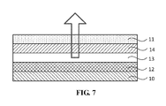
- FIG. 7 is a cross sectional view of a structure of yet another organic light-emitting display panel according to one embodiment of the present disclosure.
- the organic light-emitting display panel in the organic light-emitting display panel, only the first electrode 11 is taken as an emergent light side electrode, and light is emitted out via the first electrode 11 after being formed in the light-emitting layer 13 .
- Such an organic light-emitting display panel is also referred to as an inverted top-emission type organic light-emitting display panel.
- the materials of both the first electrode 11 and the second electrode 12 are silver or silver-containing metallic materials.
- the thickness of the second electrode 12 may be set as greater than 30 nm, and the thickness of the emergent light side electrode (the first electrode 11 ) may be set as less than 30 nm.
- Experimental Group is an inverted top-emission type organic light-emitting display panel according to the present application.
- Contrast Group is an existing upright top-emission type organic light-emitting display panel.
- Bias Voltage refers to a bias voltage applied by the first electrode 11 and the second electrode 12 on the organic light-emitting display panel.
- Lifetime refers to the working time of an organic light-emitting display panel for which the luminance of the organic light-emitting display panel attenuates from initial lightness to 95% of the initial lightness. It should be noted that, in Table 2, the bias voltage, the external quantum efficiency and the lifetime of the organic light-emitting display panels in Contrast Group and Experimental Group are all measured under the same experimental conditions (including the same current density).
- the bias voltage required for the inverted top-emission type organic light-emitting display panel in Experimental Group is identical with the bias voltage of the upright top-emission type organic light-emitting display panel in Contrast Group.
- the external quantum efficiency of the inverted top-emission type organic light-emitting display panel in Experimental Group is somewhat higher than that of the upright top-emission type organic light-emitting display panel in Contrast Group, and the lifetime of the inverted top-emission type organic light-emitting display panel in Experimental Group is much longer than that of the upright top-emission type organic light-emitting display panel in Contrast Group. This indicates that, the performance of the organic light-emitting display panel according to the embodiments of the present application is better than that of the existing organic light-emitting display panels.
- FIG. 8 is a cross sectional view of a structure of yet another organic light-emitting display panel according to one embodiment of the present disclosure.
- both the first electrode 11 and the second electrode 12 are taken as emergent light side electrodes, and after being formed in the light-emitting layer 13 , one part of the light is emitted out via the first electrode 11 , and the other part of the light is emitted out via the second electrode 12 .
- the thickness of the emergent light side electrodes may be set as less than 30 nm.
- FIG. 9 is a cross sectional view of a structure of yet another organic light-emitting display panel according to one embodiment of the present disclosure.
- the organic light-emitting display panel may further include an optical coupling layer 20 .
- the optical coupling layer 20 is located on one side of the emergent light side electrode of the organic light-emitting display panel that is facing away from the light-emitting layer 13 .
- the first electrode 11 is the emergent light side electrode
- the optical coupling layer 20 is located on one side of the first electrode 11 of the organic light-emitting display panel that is facing away from the light-emitting layer 13 .
- the process in which the light is emitted from the emergent light side electrode (the first electrode 11 ) into the air will essentially be a process in which the light is emitted from an optically denser medium into an optically thinner medium.
- the light tends to be reflected on the interface between the emergent light side electrode (the first electrode 11 ) and the air, and hence the light transmittance will be lowered.
- the arrangement of the optical coupling layer 20 is essentially to change the refractive index of the contact surface between the emergent light side of the organic light-emitting display panel and the air so as to suppress the reflection of light, thereby improving the light transmittance.
- the material of the light-emitting layer 13 may be an organic material doped with a light-emitting material.
- the light-emitting material may red light-emitting material, green light-emitting material or blue light-emitting material.
- the light emitted by the red light-emitting material, the light emitted by the green light-emitting material and the light emitted by the blue light-emitting material are mixed to obtain white light.
- the mass ratio of the light-emitting material is greater than or equal to 1% and is less than or equal to 20%.
- the organic material in the light-emitting layer 13 may only include certain organic material, or it may be a mixture of a plurality of organic materials, which is not limited in the present disclosure.
- FIG. 10 is a top view of an organic light-emitting display device according to one embodiment of the present disclosure.
- the organic light-emitting display device 101 includes any organic light-emitting display panel 201 according to the embodiments of the present disclosure.
- the organic light-emitting display device 101 may be a mobile phone, a notebook computer, an intelligent wearable device and an information inquiry machine in a public hall.
- the material of both the first electrode and the second electrode in its internal organic light-emitting display panel is silver or silver-containing metallic material
- the material of the first hole transport layer is a conductive material doped with a P-type semiconductor material or a P-type semiconductor material layer is provided between the first hole transport layer and the first electrode.
- the organic light-emitting display device can adjust the charge balance in the organic light-emitting display panel and lower the bias voltage required by the organic light-emitting display panel, thus improving the light-emitting efficiency of the organic light-emitting display panel and prolonging the lifetime of the organic light-emitting display panel.
Landscapes
- Physics & Mathematics (AREA)
- Optics & Photonics (AREA)
- Electroluminescent Light Sources (AREA)
Abstract
Description
| TABLE 1 | ||||
| External Quantum | ||||
| Bias Voltage | Efficiency | Lifetime | ||
| Experimental Group | 4 V | 6% | 100 hours |
| Contrast Group | 4 V | 6% | 70 hours |
| TABLE 2 | ||||
| External Quantum | ||||
| Bias Voltage | Efficiency | Lifetime | ||
| Experimental Group | 4 V | 10.5% | 100 hours |
| Contrast Group | 4 |
10% | 50 hours |
Claims (20)
Priority Applications (1)
| Application Number | Priority Date | Filing Date | Title |
|---|---|---|---|
| US16/203,462 US10615359B2 (en) | 2017-01-16 | 2018-11-28 | Organic light-emitting display panel and device |
Applications Claiming Priority (3)
| Application Number | Priority Date | Filing Date | Title |
|---|---|---|---|
| CN201710028398 | 2017-01-16 | ||
| CN201710028398.3A CN106549113B (en) | 2017-01-16 | 2017-01-16 | A kind of organic light emitting display panel and device |
| CN201710028398.3 | 2017-01-16 |
Related Child Applications (1)
| Application Number | Title | Priority Date | Filing Date |
|---|---|---|---|
| US16/203,462 Continuation US10615359B2 (en) | 2017-01-16 | 2018-11-28 | Organic light-emitting display panel and device |
Publications (2)
| Publication Number | Publication Date |
|---|---|
| US20180033996A1 US20180033996A1 (en) | 2018-02-01 |
| US10177332B2 true US10177332B2 (en) | 2019-01-08 |
Family
ID=58398579
Family Applications (2)
| Application Number | Title | Priority Date | Filing Date |
|---|---|---|---|
| US15/717,798 Active US10177332B2 (en) | 2017-01-16 | 2017-09-27 | Organic light-emitting display panel and device |
| US16/203,462 Active US10615359B2 (en) | 2017-01-16 | 2018-11-28 | Organic light-emitting display panel and device |
Family Applications After (1)
| Application Number | Title | Priority Date | Filing Date |
|---|---|---|---|
| US16/203,462 Active US10615359B2 (en) | 2017-01-16 | 2018-11-28 | Organic light-emitting display panel and device |
Country Status (3)
| Country | Link |
|---|---|
| US (2) | US10177332B2 (en) |
| CN (1) | CN106549113B (en) |
| DE (1) | DE102017124157B4 (en) |
Families Citing this family (6)
| Publication number | Priority date | Publication date | Assignee | Title |
|---|---|---|---|---|
| CN109004092A (en) * | 2018-06-29 | 2018-12-14 | 云谷(固安)科技有限公司 | Organic electroluminescence device and organic electroluminescence device |
| CN109768178B (en) * | 2019-01-22 | 2021-03-30 | 京东方科技集团股份有限公司 | Organic electroluminescent device, display substrate, display device |
| US20220302408A1 (en) * | 2019-08-27 | 2022-09-22 | Oti Lumionics Inc. | Light transmissive electrode for light emitting devices |
| CN110931524A (en) * | 2019-11-22 | 2020-03-27 | 深圳市华星光电半导体显示技术有限公司 | Display panel, preparation method thereof and display device |
| CN110931650A (en) | 2019-11-22 | 2020-03-27 | 深圳市华星光电半导体显示技术有限公司 | Organic light-emitting diode device, display panel and preparation method of display panel |
| CN113066934B (en) * | 2021-03-12 | 2023-05-09 | 武汉华星光电半导体显示技术有限公司 | Display panel and mobile terminal |
Citations (15)
| Publication number | Priority date | Publication date | Assignee | Title |
|---|---|---|---|---|
| US20080042556A1 (en) * | 2006-08-18 | 2008-02-21 | Chunghwa Picture Tubes, Ltd | Organic light emitting structure |
| US20080246394A1 (en) * | 2007-04-03 | 2008-10-09 | Fujikura Ltd. | Organic light-emitting diode element and optical interconnection module |
| CN101692484A (en) | 2009-08-17 | 2010-04-07 | 深圳丹邦投资集团有限公司 | Organic light-emitting device with inverted structure and manufacturing method thereof |
| CN102694125A (en) | 2011-03-21 | 2012-09-26 | 海洋王照明科技股份有限公司 | Organic electroluminescent device |
| CN103378297A (en) | 2012-04-25 | 2013-10-30 | 群康科技(深圳)有限公司 | Organic light emitting diode and display device including same |
| CN103594659A (en) | 2012-08-17 | 2014-02-19 | 海洋王照明科技股份有限公司 | Organic electroluminescent device and preparation method thereof |
| CN103927042A (en) | 2013-10-31 | 2014-07-16 | 上海中航光电子有限公司 | Touch point positioning method and device and electronic device |
| US20140234999A1 (en) * | 2011-05-11 | 2014-08-21 | Qd Vision, Inc. | Method for processing devices including quantum dots and devices |
| CN104051653A (en) | 2013-03-11 | 2014-09-17 | 海洋王照明科技股份有限公司 | Inversion-type organic light-emitting device and preparation method thereof |
| US20160027860A1 (en) * | 2014-07-23 | 2016-01-28 | Konica Minolta, Inc. | Organic electroluminescent module and method of manufacturing the same |
| US20160035980A1 (en) * | 2013-11-11 | 2016-02-04 | Boe Technology Group Co., Ltd. | Display panel and manufacturing method thereof, and display device |
| CN105845834A (en) | 2016-04-07 | 2016-08-10 | 上海大学 | Inverted green light quantum dot film electroluminescence device |
| US20160248019A1 (en) * | 2012-11-28 | 2016-08-25 | Lms Co., Ltd | Novel Compound, and Light-Emitting Element and Electronic Device Comprising Same |
| US20170098782A1 (en) * | 2015-10-05 | 2017-04-06 | Samsung Display Co., Ltd. | Organic electroluminescent device and display including the same |
| US20170263876A1 (en) * | 2016-03-10 | 2017-09-14 | Samsung Display Co., Ltd. | Organic light-emitting device |
Family Cites Families (9)
| Publication number | Priority date | Publication date | Assignee | Title |
|---|---|---|---|---|
| CN100593357C (en) * | 2005-12-21 | 2010-03-03 | 友达光电股份有限公司 | Organic Electroluminescent Devices |
| US7728512B2 (en) | 2007-03-02 | 2010-06-01 | Universal Display Corporation | Organic light emitting device having an external microcavity |
| JP2009205928A (en) | 2008-02-27 | 2009-09-10 | Fuji Electric Holdings Co Ltd | Resonant cavity color conversion el device and organic el display device using the same |
| US8476624B1 (en) * | 2012-06-01 | 2013-07-02 | Au Optronics Corporation | Organic light emitting diode (OLED) device |
| US9768403B2 (en) * | 2013-10-30 | 2017-09-19 | Sharp Kabushiki Kaisha | Organic electroluminescent element and organic electroluminescent display panel |
| CN103715372B (en) * | 2013-12-26 | 2017-08-25 | 京东方科技集团股份有限公司 | OLED display panel and preparation method thereof |
| JP6307993B2 (en) * | 2014-04-07 | 2018-04-11 | コニカミノルタ株式会社 | ORGANIC ELECTROLUMINESCENT ELEMENT AND ELECTRONIC DEVICE |
| CN105206757B (en) * | 2015-11-05 | 2016-09-07 | 京东方科技集团股份有限公司 | Organic light emitting diode, manufacturing method thereof, display substrate and display device |
| KR101700558B1 (en) * | 2016-04-20 | 2017-01-31 | 엘지디스플레이 주식회사 | Organic light emitting display device |
-
2017
- 2017-01-16 CN CN201710028398.3A patent/CN106549113B/en active Active
- 2017-09-27 US US15/717,798 patent/US10177332B2/en active Active
- 2017-10-17 DE DE102017124157.4A patent/DE102017124157B4/en active Active
-
2018
- 2018-11-28 US US16/203,462 patent/US10615359B2/en active Active
Patent Citations (15)
| Publication number | Priority date | Publication date | Assignee | Title |
|---|---|---|---|---|
| US20080042556A1 (en) * | 2006-08-18 | 2008-02-21 | Chunghwa Picture Tubes, Ltd | Organic light emitting structure |
| US20080246394A1 (en) * | 2007-04-03 | 2008-10-09 | Fujikura Ltd. | Organic light-emitting diode element and optical interconnection module |
| CN101692484A (en) | 2009-08-17 | 2010-04-07 | 深圳丹邦投资集团有限公司 | Organic light-emitting device with inverted structure and manufacturing method thereof |
| CN102694125A (en) | 2011-03-21 | 2012-09-26 | 海洋王照明科技股份有限公司 | Organic electroluminescent device |
| US20140234999A1 (en) * | 2011-05-11 | 2014-08-21 | Qd Vision, Inc. | Method for processing devices including quantum dots and devices |
| CN103378297A (en) | 2012-04-25 | 2013-10-30 | 群康科技(深圳)有限公司 | Organic light emitting diode and display device including same |
| CN103594659A (en) | 2012-08-17 | 2014-02-19 | 海洋王照明科技股份有限公司 | Organic electroluminescent device and preparation method thereof |
| US20160248019A1 (en) * | 2012-11-28 | 2016-08-25 | Lms Co., Ltd | Novel Compound, and Light-Emitting Element and Electronic Device Comprising Same |
| CN104051653A (en) | 2013-03-11 | 2014-09-17 | 海洋王照明科技股份有限公司 | Inversion-type organic light-emitting device and preparation method thereof |
| CN103927042A (en) | 2013-10-31 | 2014-07-16 | 上海中航光电子有限公司 | Touch point positioning method and device and electronic device |
| US20160035980A1 (en) * | 2013-11-11 | 2016-02-04 | Boe Technology Group Co., Ltd. | Display panel and manufacturing method thereof, and display device |
| US20160027860A1 (en) * | 2014-07-23 | 2016-01-28 | Konica Minolta, Inc. | Organic electroluminescent module and method of manufacturing the same |
| US20170098782A1 (en) * | 2015-10-05 | 2017-04-06 | Samsung Display Co., Ltd. | Organic electroluminescent device and display including the same |
| US20170263876A1 (en) * | 2016-03-10 | 2017-09-14 | Samsung Display Co., Ltd. | Organic light-emitting device |
| CN105845834A (en) | 2016-04-07 | 2016-08-10 | 上海大学 | Inverted green light quantum dot film electroluminescence device |
Non-Patent Citations (1)
| Title |
|---|
| CN second Office Action, dated Apr. 20, 2018. |
Also Published As
| Publication number | Publication date |
|---|---|
| US20180033996A1 (en) | 2018-02-01 |
| DE102017124157A1 (en) | 2018-07-19 |
| US10615359B2 (en) | 2020-04-07 |
| DE102017124157B4 (en) | 2023-08-03 |
| CN106549113B (en) | 2019-10-01 |
| CN106549113A (en) | 2017-03-29 |
| US20190109292A1 (en) | 2019-04-11 |
Similar Documents
| Publication | Publication Date | Title |
|---|---|---|
| US10615359B2 (en) | Organic light-emitting display panel and device | |
| US20180013098A1 (en) | Organic Light-Emitting Display Panel and Device | |
| US10950665B2 (en) | Organic light emitting display device | |
| US9088001B2 (en) | Organic light emitting display and method for fabricating the same | |
| US20150090984A1 (en) | Organic light emitting display device | |
| US10497879B2 (en) | Organic light-emitting display panel device | |
| CN106653803A (en) | Organic light emitting display panel and organic light emitting display device | |
| US9231228B2 (en) | Anode containing metal oxide and organic light emitting device having the same | |
| CN108539034A (en) | Organic light emitting display panel and organic light-emitting display device | |
| CN110752307B (en) | Light emitting device and display panel | |
| KR101223615B1 (en) | Inverted organic light-emitting diode and flat display device comprising the same | |
| CN106856225B (en) | A kind of organic light emitting display panel and device | |
| US8093587B2 (en) | Organic el device and process of producing the same | |
| KR102388253B1 (en) | Organic light emitting diode | |
| KR101419809B1 (en) | Inverted organic light-emitting diode and display apparatus including the same | |
| US20170250364A1 (en) | Organic light-emitting diode (oled) display panel and display apparatus | |
| KR101573762B1 (en) | Double-sided organic light-emitting diode and display device and illumination | |
| KR101258610B1 (en) | Inverted organic light-emitting diode and flat display device comprising the same | |
| US20170301875A1 (en) | Organic light-emitting display panel and device | |
| US10177333B2 (en) | Organic light-emitting display panel and device | |
| KR102362111B1 (en) | Organic light emitting display device | |
| US20150144903A1 (en) | Organic light emitting diode device | |
| US20250040338A1 (en) | Display panels | |
| US20240423008A1 (en) | Organic light-emitting display panels and display devices | |
| KR101468063B1 (en) | Double-sided organic light-emitting diode and display device and illumination |
Legal Events
| Date | Code | Title | Description |
|---|---|---|---|
| FEPP | Fee payment procedure |
Free format text: ENTITY STATUS SET TO UNDISCOUNTED (ORIGINAL EVENT CODE: BIG.); ENTITY STATUS OF PATENT OWNER: LARGE ENTITY |
|
| AS | Assignment |
Owner name: SHANGHAI TIANMA AM-OLED CO., LTD., CHINA Free format text: ASSIGNMENT OF ASSIGNORS INTEREST;ASSIGNORS:WANG, XIANGCHENG;NIU, JINGHUA;HAMADA, YUJI;AND OTHERS;REEL/FRAME:043730/0871 Effective date: 20170912 |
|
| STCF | Information on status: patent grant |
Free format text: PATENTED CASE |
|
| AS | Assignment |
Owner name: WUHAN TIANMA MICROELECTRONICS CO., LTD. SHANGHAI BRANCH, CHINA Free format text: ASSIGNMENT OF ASSIGNORS INTEREST;ASSIGNOR:SHANGHAI TIANMA AM-OLED CO.,LTD.;REEL/FRAME:059498/0307 Effective date: 20220301 Owner name: WUHAN TIANMA MICRO-ELECTRONICS CO., LTD., CHINA Free format text: ASSIGNMENT OF ASSIGNORS INTEREST;ASSIGNOR:SHANGHAI TIANMA AM-OLED CO.,LTD.;REEL/FRAME:059498/0307 Effective date: 20220301 Owner name: WUHAN TIANMA MICRO-ELECTRONICS CO., LTD., CHINA Free format text: ASSIGNMENT OF ASSIGNOR'S INTEREST;ASSIGNOR:SHANGHAI TIANMA AM-OLED CO.,LTD.;REEL/FRAME:059498/0307 Effective date: 20220301 Owner name: WUHAN TIANMA MICROELECTRONICS CO., LTD. SHANGHAI BRANCH, CHINA Free format text: ASSIGNMENT OF ASSIGNOR'S INTEREST;ASSIGNOR:SHANGHAI TIANMA AM-OLED CO.,LTD.;REEL/FRAME:059498/0307 Effective date: 20220301 |
|
| MAFP | Maintenance fee payment |
Free format text: PAYMENT OF MAINTENANCE FEE, 4TH YEAR, LARGE ENTITY (ORIGINAL EVENT CODE: M1551); ENTITY STATUS OF PATENT OWNER: LARGE ENTITY Year of fee payment: 4 |