US10177046B2 - Vertical FET with different channel orientations for NFET and PFET - Google Patents
Vertical FET with different channel orientations for NFET and PFET Download PDFInfo
- Publication number
- US10177046B2 US10177046B2 US15/436,013 US201715436013A US10177046B2 US 10177046 B2 US10177046 B2 US 10177046B2 US 201715436013 A US201715436013 A US 201715436013A US 10177046 B2 US10177046 B2 US 10177046B2
- Authority
- US
- United States
- Prior art keywords
- drain
- source
- fins
- surface orientation
- transport direction
- Prior art date
- Legal status (The legal status is an assumption and is not a legal conclusion. Google has not performed a legal analysis and makes no representation as to the accuracy of the status listed.)
- Expired - Fee Related
Links
- 239000004065 semiconductor Substances 0.000 claims abstract description 91
- 238000000034 method Methods 0.000 claims abstract description 39
- 230000005669 field effect Effects 0.000 claims abstract description 14
- XUIMIQQOPSSXEZ-UHFFFAOYSA-N Silicon Chemical compound [Si] XUIMIQQOPSSXEZ-UHFFFAOYSA-N 0.000 claims description 18
- 229910052710 silicon Inorganic materials 0.000 claims description 18
- 239000010703 silicon Substances 0.000 claims description 18
- 239000000758 substrate Substances 0.000 abstract description 75
- 239000000463 material Substances 0.000 description 62
- 239000010410 layer Substances 0.000 description 59
- 125000006850 spacer group Chemical group 0.000 description 43
- 230000015572 biosynthetic process Effects 0.000 description 26
- 238000000151 deposition Methods 0.000 description 17
- 238000005530 etching Methods 0.000 description 15
- 229910052751 metal Inorganic materials 0.000 description 15
- 239000002184 metal Substances 0.000 description 15
- 239000003989 dielectric material Substances 0.000 description 14
- 238000002955 isolation Methods 0.000 description 14
- 230000008021 deposition Effects 0.000 description 13
- VYPSYNLAJGMNEJ-UHFFFAOYSA-N Silicium dioxide Chemical compound O=[Si]=O VYPSYNLAJGMNEJ-UHFFFAOYSA-N 0.000 description 10
- 239000013078 crystal Substances 0.000 description 9
- 229910052814 silicon oxide Inorganic materials 0.000 description 9
- 238000005229 chemical vapour deposition Methods 0.000 description 7
- 239000002019 doping agent Substances 0.000 description 7
- 238000005240 physical vapour deposition Methods 0.000 description 7
- 238000005137 deposition process Methods 0.000 description 6
- 239000011241 protective layer Substances 0.000 description 6
- 235000012431 wafers Nutrition 0.000 description 6
- 238000001459 lithography Methods 0.000 description 5
- 239000000203 mixture Substances 0.000 description 5
- 150000004767 nitrides Chemical class 0.000 description 5
- 238000000623 plasma-assisted chemical vapour deposition Methods 0.000 description 5
- 238000000231 atomic layer deposition Methods 0.000 description 4
- 238000005516 engineering process Methods 0.000 description 4
- 238000002360 preparation method Methods 0.000 description 4
- 239000000126 substance Substances 0.000 description 4
- 229910000577 Silicon-germanium Inorganic materials 0.000 description 3
- 238000004519 manufacturing process Methods 0.000 description 3
- 239000007769 metal material Substances 0.000 description 3
- 238000012986 modification Methods 0.000 description 3
- 230000004048 modification Effects 0.000 description 3
- -1 oxynitrides Chemical class 0.000 description 3
- 238000000059 patterning Methods 0.000 description 3
- 239000000376 reactant Substances 0.000 description 3
- 229910021483 silicon-carbon alloy Inorganic materials 0.000 description 3
- PXHVJJICTQNCMI-UHFFFAOYSA-N Nickel Chemical compound [Ni] PXHVJJICTQNCMI-UHFFFAOYSA-N 0.000 description 2
- KDLHZDBZIXYQEI-UHFFFAOYSA-N Palladium Chemical compound [Pd] KDLHZDBZIXYQEI-UHFFFAOYSA-N 0.000 description 2
- 229910004205 SiNX Inorganic materials 0.000 description 2
- LEVVHYCKPQWKOP-UHFFFAOYSA-N [Si].[Ge] Chemical compound [Si].[Ge] LEVVHYCKPQWKOP-UHFFFAOYSA-N 0.000 description 2
- 229910052782 aluminium Inorganic materials 0.000 description 2
- XAGFODPZIPBFFR-UHFFFAOYSA-N aluminium Chemical compound [Al] XAGFODPZIPBFFR-UHFFFAOYSA-N 0.000 description 2
- 238000000137 annealing Methods 0.000 description 2
- 239000000969 carrier Substances 0.000 description 2
- 150000001875 compounds Chemical class 0.000 description 2
- 230000008878 coupling Effects 0.000 description 2
- 238000010168 coupling process Methods 0.000 description 2
- 238000005859 coupling reaction Methods 0.000 description 2
- 239000002178 crystalline material Substances 0.000 description 2
- 238000002050 diffraction method Methods 0.000 description 2
- 238000004070 electrodeposition Methods 0.000 description 2
- 230000008020 evaporation Effects 0.000 description 2
- 238000001704 evaporation Methods 0.000 description 2
- 239000004615 ingredient Substances 0.000 description 2
- 150000002500 ions Chemical class 0.000 description 2
- MRELNEQAGSRDBK-UHFFFAOYSA-N lanthanum(3+);oxygen(2-) Chemical compound [O-2].[O-2].[O-2].[La+3].[La+3] MRELNEQAGSRDBK-UHFFFAOYSA-N 0.000 description 2
- 229910044991 metal oxide Inorganic materials 0.000 description 2
- 150000004706 metal oxides Chemical class 0.000 description 2
- 150000002739 metals Chemical class 0.000 description 2
- 229920002120 photoresistant polymer Polymers 0.000 description 2
- BASFCYQUMIYNBI-UHFFFAOYSA-N platinum Chemical compound [Pt] BASFCYQUMIYNBI-UHFFFAOYSA-N 0.000 description 2
- 238000012545 processing Methods 0.000 description 2
- 238000004151 rapid thermal annealing Methods 0.000 description 2
- 229910000951 Aluminide Inorganic materials 0.000 description 1
- JBRZTFJDHDCESZ-UHFFFAOYSA-N AsGa Chemical compound [As]#[Ga] JBRZTFJDHDCESZ-UHFFFAOYSA-N 0.000 description 1
- OKTJSMMVPCPJKN-UHFFFAOYSA-N Carbon Chemical compound [C] OKTJSMMVPCPJKN-UHFFFAOYSA-N 0.000 description 1
- 229910000927 Ge alloy Inorganic materials 0.000 description 1
- GPXJNWSHGFTCBW-UHFFFAOYSA-N Indium phosphide Chemical compound [In]#P GPXJNWSHGFTCBW-UHFFFAOYSA-N 0.000 description 1
- KJTLSVCANCCWHF-UHFFFAOYSA-N Ruthenium Chemical compound [Ru] KJTLSVCANCCWHF-UHFFFAOYSA-N 0.000 description 1
- 229910000676 Si alloy Inorganic materials 0.000 description 1
- 229910052581 Si3N4 Inorganic materials 0.000 description 1
- GWEVSGVZZGPLCZ-UHFFFAOYSA-N Titan oxide Chemical compound O=[Ti]=O GWEVSGVZZGPLCZ-UHFFFAOYSA-N 0.000 description 1
- RTAQQCXQSZGOHL-UHFFFAOYSA-N Titanium Chemical compound [Ti] RTAQQCXQSZGOHL-UHFFFAOYSA-N 0.000 description 1
- QCWXUUIWCKQGHC-UHFFFAOYSA-N Zirconium Chemical compound [Zr] QCWXUUIWCKQGHC-UHFFFAOYSA-N 0.000 description 1
- 229910026551 ZrC Inorganic materials 0.000 description 1
- OTCHGXYCWNXDOA-UHFFFAOYSA-N [C].[Zr] Chemical compound [C].[Zr] OTCHGXYCWNXDOA-UHFFFAOYSA-N 0.000 description 1
- XWCMFHPRATWWFO-UHFFFAOYSA-N [O-2].[Ta+5].[Sc+3].[O-2].[O-2].[O-2] Chemical compound [O-2].[Ta+5].[Sc+3].[O-2].[O-2].[O-2] XWCMFHPRATWWFO-UHFFFAOYSA-N 0.000 description 1
- CEPICIBPGDWCRU-UHFFFAOYSA-N [Si].[Hf] Chemical compound [Si].[Hf] CEPICIBPGDWCRU-UHFFFAOYSA-N 0.000 description 1
- ILCYGSITMBHYNK-UHFFFAOYSA-N [Si]=O.[Hf] Chemical compound [Si]=O.[Hf] ILCYGSITMBHYNK-UHFFFAOYSA-N 0.000 description 1
- CAVCGVPGBKGDTG-UHFFFAOYSA-N alumanylidynemethyl(alumanylidynemethylalumanylidenemethylidene)alumane Chemical compound [Al]#C[Al]=C=[Al]C#[Al] CAVCGVPGBKGDTG-UHFFFAOYSA-N 0.000 description 1
- 150000004645 aluminates Chemical class 0.000 description 1
- 150000004945 aromatic hydrocarbons Chemical class 0.000 description 1
- VKJLWXGJGDEGSO-UHFFFAOYSA-N barium(2+);oxygen(2-);titanium(4+) Chemical compound [O-2].[O-2].[O-2].[Ti+4].[Ba+2] VKJLWXGJGDEGSO-UHFFFAOYSA-N 0.000 description 1
- 229910002056 binary alloy Inorganic materials 0.000 description 1
- 229910052799 carbon Inorganic materials 0.000 description 1
- 238000000224 chemical solution deposition Methods 0.000 description 1
- 229910017052 cobalt Inorganic materials 0.000 description 1
- 239000010941 cobalt Substances 0.000 description 1
- GUTLYIVDDKVIGB-UHFFFAOYSA-N cobalt atom Chemical compound [Co] GUTLYIVDDKVIGB-UHFFFAOYSA-N 0.000 description 1
- 239000000306 component Substances 0.000 description 1
- 239000012141 concentrate Substances 0.000 description 1
- 239000000470 constituent Substances 0.000 description 1
- 230000001419 dependent effect Effects 0.000 description 1
- 238000009792 diffusion process Methods 0.000 description 1
- 238000000609 electron-beam lithography Methods 0.000 description 1
- 238000011049 filling Methods 0.000 description 1
- 229910052732 germanium Inorganic materials 0.000 description 1
- GNPVGFCGXDBREM-UHFFFAOYSA-N germanium atom Chemical compound [Ge] GNPVGFCGXDBREM-UHFFFAOYSA-N 0.000 description 1
- 239000011521 glass Substances 0.000 description 1
- 238000000227 grinding Methods 0.000 description 1
- 229910052735 hafnium Inorganic materials 0.000 description 1
- VBJZVLUMGGDVMO-UHFFFAOYSA-N hafnium atom Chemical compound [Hf] VBJZVLUMGGDVMO-UHFFFAOYSA-N 0.000 description 1
- 229910000449 hafnium oxide Inorganic materials 0.000 description 1
- WIHZLLGSGQNAGK-UHFFFAOYSA-N hafnium(4+);oxygen(2-) Chemical compound [O-2].[O-2].[Hf+4] WIHZLLGSGQNAGK-UHFFFAOYSA-N 0.000 description 1
- WHJFNYXPKGDKBB-UHFFFAOYSA-N hafnium;methane Chemical compound C.[Hf] WHJFNYXPKGDKBB-UHFFFAOYSA-N 0.000 description 1
- RPQDHPTXJYYUPQ-UHFFFAOYSA-N indium arsenide Chemical compound [In]#[As] RPQDHPTXJYYUPQ-UHFFFAOYSA-N 0.000 description 1
- 238000005468 ion implantation Methods 0.000 description 1
- 229910052746 lanthanum Inorganic materials 0.000 description 1
- FZLIPJUXYLNCLC-UHFFFAOYSA-N lanthanum atom Chemical compound [La] FZLIPJUXYLNCLC-UHFFFAOYSA-N 0.000 description 1
- JQJCSZOEVBFDKO-UHFFFAOYSA-N lead zinc Chemical compound [Zn].[Pb] JQJCSZOEVBFDKO-UHFFFAOYSA-N 0.000 description 1
- 239000007788 liquid Substances 0.000 description 1
- 238000013208 measuring procedure Methods 0.000 description 1
- 150000001247 metal acetylides Chemical class 0.000 description 1
- 229910052914 metal silicate Inorganic materials 0.000 description 1
- 238000004377 microelectronic Methods 0.000 description 1
- 238000001451 molecular beam epitaxy Methods 0.000 description 1
- 229910052759 nickel Inorganic materials 0.000 description 1
- TWNQGVIAIRXVLR-UHFFFAOYSA-N oxo(oxoalumanyloxy)alumane Chemical compound O=[Al]O[Al]=O TWNQGVIAIRXVLR-UHFFFAOYSA-N 0.000 description 1
- KJXBRHIPHIVJCS-UHFFFAOYSA-N oxo(oxoalumanyloxy)lanthanum Chemical compound O=[Al]O[La]=O KJXBRHIPHIVJCS-UHFFFAOYSA-N 0.000 description 1
- SIWVEOZUMHYXCS-UHFFFAOYSA-N oxo(oxoyttriooxy)yttrium Chemical compound O=[Y]O[Y]=O SIWVEOZUMHYXCS-UHFFFAOYSA-N 0.000 description 1
- BPUBBGLMJRNUCC-UHFFFAOYSA-N oxygen(2-);tantalum(5+) Chemical compound [O-2].[O-2].[O-2].[O-2].[O-2].[Ta+5].[Ta+5] BPUBBGLMJRNUCC-UHFFFAOYSA-N 0.000 description 1
- RVTZCBVAJQQJTK-UHFFFAOYSA-N oxygen(2-);zirconium(4+) Chemical compound [O-2].[O-2].[Zr+4] RVTZCBVAJQQJTK-UHFFFAOYSA-N 0.000 description 1
- 229910052763 palladium Inorganic materials 0.000 description 1
- 239000002245 particle Substances 0.000 description 1
- 230000000737 periodic effect Effects 0.000 description 1
- 238000000206 photolithography Methods 0.000 description 1
- 238000005268 plasma chemical vapour deposition Methods 0.000 description 1
- 238000007747 plating Methods 0.000 description 1
- 229910052697 platinum Inorganic materials 0.000 description 1
- 238000005498 polishing Methods 0.000 description 1
- 229920000642 polymer Polymers 0.000 description 1
- 229910002059 quaternary alloy Inorganic materials 0.000 description 1
- 229910052707 ruthenium Inorganic materials 0.000 description 1
- 238000005389 semiconductor device fabrication Methods 0.000 description 1
- 238000007493 shaping process Methods 0.000 description 1
- 150000004760 silicates Chemical class 0.000 description 1
- HQVNEWCFYHHQES-UHFFFAOYSA-N silicon nitride Chemical compound N12[Si]34N5[Si]62N3[Si]51N64 HQVNEWCFYHHQES-UHFFFAOYSA-N 0.000 description 1
- UVGLBOPDEUYYCS-UHFFFAOYSA-N silicon zirconium Chemical compound [Si].[Zr] UVGLBOPDEUYYCS-UHFFFAOYSA-N 0.000 description 1
- 239000007787 solid Substances 0.000 description 1
- 238000004544 sputter deposition Methods 0.000 description 1
- VEALVRVVWBQVSL-UHFFFAOYSA-N strontium titanate Chemical compound [Sr+2].[O-][Ti]([O-])=O VEALVRVVWBQVSL-UHFFFAOYSA-N 0.000 description 1
- CZXRMHUWVGPWRM-UHFFFAOYSA-N strontium;barium(2+);oxygen(2-);titanium(4+) Chemical compound [O-2].[O-2].[O-2].[O-2].[Ti+4].[Sr+2].[Ba+2] CZXRMHUWVGPWRM-UHFFFAOYSA-N 0.000 description 1
- 229910052715 tantalum Inorganic materials 0.000 description 1
- GUVRBAGPIYLISA-UHFFFAOYSA-N tantalum atom Chemical compound [Ta] GUVRBAGPIYLISA-UHFFFAOYSA-N 0.000 description 1
- 229910001936 tantalum oxide Inorganic materials 0.000 description 1
- 229910002058 ternary alloy Inorganic materials 0.000 description 1
- 229910052719 titanium Inorganic materials 0.000 description 1
- 239000010936 titanium Substances 0.000 description 1
- OGIDPMRJRNCKJF-UHFFFAOYSA-N titanium oxide Inorganic materials [Ti]=O OGIDPMRJRNCKJF-UHFFFAOYSA-N 0.000 description 1
- MTPVUVINMAGMJL-UHFFFAOYSA-N trimethyl(1,1,2,2,2-pentafluoroethyl)silane Chemical compound C[Si](C)(C)C(F)(F)C(F)(F)F MTPVUVINMAGMJL-UHFFFAOYSA-N 0.000 description 1
- 229910052726 zirconium Inorganic materials 0.000 description 1
- 229910001928 zirconium oxide Inorganic materials 0.000 description 1
- GFQYVLUOOAAOGM-UHFFFAOYSA-N zirconium(iv) silicate Chemical compound [Zr+4].[O-][Si]([O-])([O-])[O-] GFQYVLUOOAAOGM-UHFFFAOYSA-N 0.000 description 1
Images
Classifications
-
- H—ELECTRICITY
- H01—ELECTRIC ELEMENTS
- H01L—SEMICONDUCTOR DEVICES NOT COVERED BY CLASS H10
- H01L21/00—Processes or apparatus adapted for the manufacture or treatment of semiconductor or solid state devices or of parts thereof
- H01L21/70—Manufacture or treatment of devices consisting of a plurality of solid state components formed in or on a common substrate or of parts thereof; Manufacture of integrated circuit devices or of parts thereof
- H01L21/77—Manufacture or treatment of devices consisting of a plurality of solid state components or integrated circuits formed in, or on, a common substrate
- H01L21/78—Manufacture or treatment of devices consisting of a plurality of solid state components or integrated circuits formed in, or on, a common substrate with subsequent division of the substrate into plural individual devices
- H01L21/82—Manufacture or treatment of devices consisting of a plurality of solid state components or integrated circuits formed in, or on, a common substrate with subsequent division of the substrate into plural individual devices to produce devices, e.g. integrated circuits, each consisting of a plurality of components
- H01L21/822—Manufacture or treatment of devices consisting of a plurality of solid state components or integrated circuits formed in, or on, a common substrate with subsequent division of the substrate into plural individual devices to produce devices, e.g. integrated circuits, each consisting of a plurality of components the substrate being a semiconductor, using silicon technology
- H01L21/8232—Field-effect technology
- H01L21/8234—MIS technology, i.e. integration processes of field effect transistors of the conductor-insulator-semiconductor type
- H01L21/8238—Complementary field-effect transistors, e.g. CMOS
- H01L21/823892—Complementary field-effect transistors, e.g. CMOS with a particular manufacturing method of the wells or tubs, e.g. twin tubs, high energy well implants, buried implanted layers for lateral isolation [BILLI]
-
- H—ELECTRICITY
- H01—ELECTRIC ELEMENTS
- H01L—SEMICONDUCTOR DEVICES NOT COVERED BY CLASS H10
- H01L21/00—Processes or apparatus adapted for the manufacture or treatment of semiconductor or solid state devices or of parts thereof
- H01L21/70—Manufacture or treatment of devices consisting of a plurality of solid state components formed in or on a common substrate or of parts thereof; Manufacture of integrated circuit devices or of parts thereof
- H01L21/77—Manufacture or treatment of devices consisting of a plurality of solid state components or integrated circuits formed in, or on, a common substrate
- H01L21/78—Manufacture or treatment of devices consisting of a plurality of solid state components or integrated circuits formed in, or on, a common substrate with subsequent division of the substrate into plural individual devices
- H01L21/82—Manufacture or treatment of devices consisting of a plurality of solid state components or integrated circuits formed in, or on, a common substrate with subsequent division of the substrate into plural individual devices to produce devices, e.g. integrated circuits, each consisting of a plurality of components
- H01L21/822—Manufacture or treatment of devices consisting of a plurality of solid state components or integrated circuits formed in, or on, a common substrate with subsequent division of the substrate into plural individual devices to produce devices, e.g. integrated circuits, each consisting of a plurality of components the substrate being a semiconductor, using silicon technology
- H01L21/8232—Field-effect technology
- H01L21/8234—MIS technology, i.e. integration processes of field effect transistors of the conductor-insulator-semiconductor type
- H01L21/8238—Complementary field-effect transistors, e.g. CMOS
- H01L21/823807—Complementary field-effect transistors, e.g. CMOS with a particular manufacturing method of the channel structures, e.g. channel implants, halo or pocket implants, or channel materials
-
- H—ELECTRICITY
- H01—ELECTRIC ELEMENTS
- H01L—SEMICONDUCTOR DEVICES NOT COVERED BY CLASS H10
- H01L21/00—Processes or apparatus adapted for the manufacture or treatment of semiconductor or solid state devices or of parts thereof
- H01L21/70—Manufacture or treatment of devices consisting of a plurality of solid state components formed in or on a common substrate or of parts thereof; Manufacture of integrated circuit devices or of parts thereof
- H01L21/77—Manufacture or treatment of devices consisting of a plurality of solid state components or integrated circuits formed in, or on, a common substrate
- H01L21/78—Manufacture or treatment of devices consisting of a plurality of solid state components or integrated circuits formed in, or on, a common substrate with subsequent division of the substrate into plural individual devices
- H01L21/82—Manufacture or treatment of devices consisting of a plurality of solid state components or integrated circuits formed in, or on, a common substrate with subsequent division of the substrate into plural individual devices to produce devices, e.g. integrated circuits, each consisting of a plurality of components
- H01L21/822—Manufacture or treatment of devices consisting of a plurality of solid state components or integrated circuits formed in, or on, a common substrate with subsequent division of the substrate into plural individual devices to produce devices, e.g. integrated circuits, each consisting of a plurality of components the substrate being a semiconductor, using silicon technology
- H01L21/8232—Field-effect technology
- H01L21/8234—MIS technology, i.e. integration processes of field effect transistors of the conductor-insulator-semiconductor type
- H01L21/8238—Complementary field-effect transistors, e.g. CMOS
- H01L21/823814—Complementary field-effect transistors, e.g. CMOS with a particular manufacturing method of the source or drain structures, e.g. specific source or drain implants or silicided source or drain structures or raised source or drain structures
-
- H—ELECTRICITY
- H01—ELECTRIC ELEMENTS
- H01L—SEMICONDUCTOR DEVICES NOT COVERED BY CLASS H10
- H01L21/00—Processes or apparatus adapted for the manufacture or treatment of semiconductor or solid state devices or of parts thereof
- H01L21/70—Manufacture or treatment of devices consisting of a plurality of solid state components formed in or on a common substrate or of parts thereof; Manufacture of integrated circuit devices or of parts thereof
- H01L21/77—Manufacture or treatment of devices consisting of a plurality of solid state components or integrated circuits formed in, or on, a common substrate
- H01L21/78—Manufacture or treatment of devices consisting of a plurality of solid state components or integrated circuits formed in, or on, a common substrate with subsequent division of the substrate into plural individual devices
- H01L21/82—Manufacture or treatment of devices consisting of a plurality of solid state components or integrated circuits formed in, or on, a common substrate with subsequent division of the substrate into plural individual devices to produce devices, e.g. integrated circuits, each consisting of a plurality of components
- H01L21/822—Manufacture or treatment of devices consisting of a plurality of solid state components or integrated circuits formed in, or on, a common substrate with subsequent division of the substrate into plural individual devices to produce devices, e.g. integrated circuits, each consisting of a plurality of components the substrate being a semiconductor, using silicon technology
- H01L21/8232—Field-effect technology
- H01L21/8234—MIS technology, i.e. integration processes of field effect transistors of the conductor-insulator-semiconductor type
- H01L21/8238—Complementary field-effect transistors, e.g. CMOS
- H01L21/823878—Complementary field-effect transistors, e.g. CMOS isolation region manufacturing related aspects, e.g. to avoid interaction of isolation region with adjacent structure
-
- H—ELECTRICITY
- H01—ELECTRIC ELEMENTS
- H01L—SEMICONDUCTOR DEVICES NOT COVERED BY CLASS H10
- H01L21/00—Processes or apparatus adapted for the manufacture or treatment of semiconductor or solid state devices or of parts thereof
- H01L21/70—Manufacture or treatment of devices consisting of a plurality of solid state components formed in or on a common substrate or of parts thereof; Manufacture of integrated circuit devices or of parts thereof
- H01L21/77—Manufacture or treatment of devices consisting of a plurality of solid state components or integrated circuits formed in, or on, a common substrate
- H01L21/78—Manufacture or treatment of devices consisting of a plurality of solid state components or integrated circuits formed in, or on, a common substrate with subsequent division of the substrate into plural individual devices
- H01L21/82—Manufacture or treatment of devices consisting of a plurality of solid state components or integrated circuits formed in, or on, a common substrate with subsequent division of the substrate into plural individual devices to produce devices, e.g. integrated circuits, each consisting of a plurality of components
- H01L21/822—Manufacture or treatment of devices consisting of a plurality of solid state components or integrated circuits formed in, or on, a common substrate with subsequent division of the substrate into plural individual devices to produce devices, e.g. integrated circuits, each consisting of a plurality of components the substrate being a semiconductor, using silicon technology
- H01L21/8232—Field-effect technology
- H01L21/8234—MIS technology, i.e. integration processes of field effect transistors of the conductor-insulator-semiconductor type
- H01L21/8238—Complementary field-effect transistors, e.g. CMOS
- H01L21/823885—Complementary field-effect transistors, e.g. CMOS with a particular manufacturing method of vertical transistor structures, i.e. with channel vertical to the substrate surface
-
- H—ELECTRICITY
- H01—ELECTRIC ELEMENTS
- H01L—SEMICONDUCTOR DEVICES NOT COVERED BY CLASS H10
- H01L27/00—Devices consisting of a plurality of semiconductor or other solid-state components formed in or on a common substrate
- H01L27/02—Devices consisting of a plurality of semiconductor or other solid-state components formed in or on a common substrate including semiconductor components specially adapted for rectifying, oscillating, amplifying or switching and having at least one potential-jump barrier or surface barrier; including integrated passive circuit elements with at least one potential-jump barrier or surface barrier
- H01L27/04—Devices consisting of a plurality of semiconductor or other solid-state components formed in or on a common substrate including semiconductor components specially adapted for rectifying, oscillating, amplifying or switching and having at least one potential-jump barrier or surface barrier; including integrated passive circuit elements with at least one potential-jump barrier or surface barrier the substrate being a semiconductor body
- H01L27/08—Devices consisting of a plurality of semiconductor or other solid-state components formed in or on a common substrate including semiconductor components specially adapted for rectifying, oscillating, amplifying or switching and having at least one potential-jump barrier or surface barrier; including integrated passive circuit elements with at least one potential-jump barrier or surface barrier the substrate being a semiconductor body including only semiconductor components of a single kind
- H01L27/085—Devices consisting of a plurality of semiconductor or other solid-state components formed in or on a common substrate including semiconductor components specially adapted for rectifying, oscillating, amplifying or switching and having at least one potential-jump barrier or surface barrier; including integrated passive circuit elements with at least one potential-jump barrier or surface barrier the substrate being a semiconductor body including only semiconductor components of a single kind including field-effect components only
- H01L27/088—Devices consisting of a plurality of semiconductor or other solid-state components formed in or on a common substrate including semiconductor components specially adapted for rectifying, oscillating, amplifying or switching and having at least one potential-jump barrier or surface barrier; including integrated passive circuit elements with at least one potential-jump barrier or surface barrier the substrate being a semiconductor body including only semiconductor components of a single kind including field-effect components only the components being field-effect transistors with insulated gate
- H01L27/092—Devices consisting of a plurality of semiconductor or other solid-state components formed in or on a common substrate including semiconductor components specially adapted for rectifying, oscillating, amplifying or switching and having at least one potential-jump barrier or surface barrier; including integrated passive circuit elements with at least one potential-jump barrier or surface barrier the substrate being a semiconductor body including only semiconductor components of a single kind including field-effect components only the components being field-effect transistors with insulated gate complementary MIS field-effect transistors
- H01L27/0928—Devices consisting of a plurality of semiconductor or other solid-state components formed in or on a common substrate including semiconductor components specially adapted for rectifying, oscillating, amplifying or switching and having at least one potential-jump barrier or surface barrier; including integrated passive circuit elements with at least one potential-jump barrier or surface barrier the substrate being a semiconductor body including only semiconductor components of a single kind including field-effect components only the components being field-effect transistors with insulated gate complementary MIS field-effect transistors comprising both N- and P- wells in the substrate, e.g. twin-tub
-
- H—ELECTRICITY
- H01—ELECTRIC ELEMENTS
- H01L—SEMICONDUCTOR DEVICES NOT COVERED BY CLASS H10
- H01L29/00—Semiconductor devices adapted for rectifying, amplifying, oscillating or switching, or capacitors or resistors with at least one potential-jump barrier or surface barrier, e.g. PN junction depletion layer or carrier concentration layer; Details of semiconductor bodies or of electrodes thereof ; Multistep manufacturing processes therefor
- H01L29/02—Semiconductor bodies ; Multistep manufacturing processes therefor
- H01L29/04—Semiconductor bodies ; Multistep manufacturing processes therefor characterised by their crystalline structure, e.g. polycrystalline, cubic or particular orientation of crystalline planes
- H01L29/045—Semiconductor bodies ; Multistep manufacturing processes therefor characterised by their crystalline structure, e.g. polycrystalline, cubic or particular orientation of crystalline planes by their particular orientation of crystalline planes
-
- H—ELECTRICITY
- H01—ELECTRIC ELEMENTS
- H01L—SEMICONDUCTOR DEVICES NOT COVERED BY CLASS H10
- H01L29/00—Semiconductor devices adapted for rectifying, amplifying, oscillating or switching, or capacitors or resistors with at least one potential-jump barrier or surface barrier, e.g. PN junction depletion layer or carrier concentration layer; Details of semiconductor bodies or of electrodes thereof ; Multistep manufacturing processes therefor
- H01L29/66—Types of semiconductor device ; Multistep manufacturing processes therefor
- H01L29/66007—Multistep manufacturing processes
- H01L29/66075—Multistep manufacturing processes of devices having semiconductor bodies comprising group 14 or group 13/15 materials
- H01L29/66227—Multistep manufacturing processes of devices having semiconductor bodies comprising group 14 or group 13/15 materials the devices being controllable only by the electric current supplied or the electric potential applied, to an electrode which does not carry the current to be rectified, amplified or switched, e.g. three-terminal devices
- H01L29/66409—Unipolar field-effect transistors
- H01L29/66477—Unipolar field-effect transistors with an insulated gate, i.e. MISFET
- H01L29/66666—Vertical transistors
-
- H—ELECTRICITY
- H01—ELECTRIC ELEMENTS
- H01L—SEMICONDUCTOR DEVICES NOT COVERED BY CLASS H10
- H01L29/00—Semiconductor devices adapted for rectifying, amplifying, oscillating or switching, or capacitors or resistors with at least one potential-jump barrier or surface barrier, e.g. PN junction depletion layer or carrier concentration layer; Details of semiconductor bodies or of electrodes thereof ; Multistep manufacturing processes therefor
- H01L29/66—Types of semiconductor device ; Multistep manufacturing processes therefor
- H01L29/68—Types of semiconductor device ; Multistep manufacturing processes therefor controllable by only the electric current supplied, or only the electric potential applied, to an electrode which does not carry the current to be rectified, amplified or switched
- H01L29/76—Unipolar devices, e.g. field effect transistors
- H01L29/772—Field effect transistors
- H01L29/78—Field effect transistors with field effect produced by an insulated gate
- H01L29/7827—Vertical transistors
Definitions
- the present invention relates in general to vertical field effect transistor (VFETs), and more specifically, to fabrication methodologies and resulting structures for providing different channel orientations for n-type VFETs and p-type VFETs.
- VFETs vertical field effect transistor
- a field effect transistor is a semiconductor device in which output current, i.e., source-drain current, is controlled by the voltage applied to a gate structure of the semiconductor device.
- An FET has three terminals, namely, a gate structure, a source region and a drain region.
- the term “drain” means a doped region in semiconductor device located at the end of the channel region, in which carriers are flowing out of the transistor through the drain.
- the term “source” is a doped region in the semiconductor device, in which majority carriers are flowing into the channel region.
- the channel region is the region underlying the gate structure and between the source and drain of the semiconductor device that becomes conductive when the semiconductor device is turned on.
- a method of forming a semiconductor device includes providing a first substrate adjacent to a second substrate.
- the first substrate has a first surface orientation
- the second substrate has a second surface orientation different from the first surface orientation.
- the method includes forming an n-type field effect transistor (NFET) device with the first substrate.
- the NFET device includes a first source, a first drain, and one or more first fins.
- the first source and the first drain have a vertical relationship with respect to the one or more first fins.
- the method includes forming a p-type field effect transistor (PFET) device with the second substrate, the PFET device including a second source, a second drain, and one or more second fins.
- the second source and the second drain have a vertical relationship with respect to the one or more second fins.
- PFET p-type field effect transistor
- a semiconductor device is provided.
- a first substrate is adjacent to a second substrate.
- the first substrate has a first surface orientation.
- the second substrate has a second surface orientation different from the first surface orientation.
- An n-type field effect transistor (NFET) device is formed with the first substrate.
- the NFET device includes a first source, a first drain, and one or more first fins.
- the first source and the first drain have a vertical relationship with respect to the one or more first fins.
- a p-type field effect transistor (PFET) device is formed with the second substrate.
- the PFET device includes a second source, a second drain, and one or more second fins.
- the second source and the second drain have a vertical relationship with respect to the one or more second fins.
- a method of forming a semiconductor device includes forming an n-type field effect transistor (NFET) device.
- the NFET device includes a first source, a first drain, a gate metal, a gate dielectric, and one or more first fins.
- the first source and the first drain have a vertical relationship with respect to the one or more first fins.
- the first source, the first drain, and the one or more first fins have a first surface orientation.
- the method includes forming a p-type field effect transistor (PFET) device.
- the PFET device includes a second source, a second drain, the gate metal, the gate dielectric, and one or more second fins.
- the second source and the second drain have a vertical relationship with respect to the one or more second fins.
- the second source, the second drain, and the one or more second fins have a second surface orientation different from the first surface orientation.
- FIG. 1 is a cross-sectional view of a VFET structure according to one or more embodiments.
- FIG. 2 is a cross-sectional view of the VFET structure depicting a (110) structure on top of a (100) structure (or vice versa) according to one or more embodiments.
- FIG. 3 is a cross-sectional view of the VFET structure depicting etching of the semiconductor substrate according to one or more embodiments.
- FIG. 4 is a cross-sectional view of the VFET structure depicting formation of a side wall spacer according to one or more embodiments.
- FIG. 5 is a cross-sectional view of the VFET structure depicting epitaxial growth of the semiconductor substrate according to one or more embodiments.
- FIG. 6 is a cross-sectional view of the VFET structure depicting planarization according to one or more embodiments.
- FIG. 7 is a cross-sectional view of the VFET structure depicting formation of the vertical fin channels according to one or more embodiments.
- FIG. 8 is a cross-sectional view of the VFET structure depicting formation of a protecting layer according to one or more embodiments.
- FIG. 9 is a cross-sectional view of the VFET structure depicting trench formation according to one or more embodiments.
- FIG. 10 is a cross-sectional view of the VFET structure depicting formation of a fill layer according to one or more embodiments.
- FIG. 11 is a cross-sectional view of the VFET structure depicting formation of the isolation regions according to one or more embodiments.
- FIG. 12 is a cross-sectional view of the VFET structure depicting formation of the high-k dielectric material according to one or more embodiments.
- FIG. 13 is a cross-sectional view of the VFET structure depicting formation of a gate material according to one or more embodiments.
- FIG. 14 is a cross-sectional view of the VFET structure depicting etching of the gate material according to one or more embodiments.
- FIG. 15 is a cross-sectional view of the VFET structure depicting top/second spacer formation according to one or more embodiments.
- FIG. 16 is a cross-sectional view of the VFET structure depicting formation of the inter-level dielectric layer according to one or more embodiments.
- FIG. 17 is a cross-sectional view of the VFET structure depicting exposure of fins according to one or more embodiments.
- FIG. 18 is a cross-sectional view of the VFET structure depicting formation of the top source/drain of the NFET device according to one or more embodiments.
- FIG. 19 is a cross-sectional view of the VFET structure depicting exposure of fins according to one or more embodiments.
- FIG. 20 is a cross-sectional view of the VFET structure depicting formation of the top source/drain of the PFET device according to one or more embodiments.
- FIG. 21 is a flow chart of a method of forming a vertical device according to one or more embodiments.
- references to forming layer “A” over layer “B” include situations in which one or more intermediate layers (e.g., layer “C”) is between layer “A” and layer “B” as long as the relevant characteristics and functionalities of layer “A” and layer “B” are not substantially changed by the intermediate layer(s).
- layer “C” one or more intermediate layers
- invention or “present invention” are non-limiting terms and not intended to refer to any single aspect of the particular invention but encompass all possible aspects as described in the specification and the claims.
- the term “about” modifying the quantity of an ingredient, component, or reactant of the invention employed refers to variation in the numerical quantity that can occur, for example, through typical measuring and liquid handling procedures used for making concentrates or solutions. Furthermore, variation can occur from inadvertent error in measuring procedures, differences in the manufacture, source, or purity of the ingredients employed to make the compositions or carry out the methods, and the like.
- the term “about” means within 10% of the reported numerical value.
- the term “about” means within 5% of the reported numerical value.
- the term “about” means within 10, 9, 8, 7, 6, 5, 4, 3, 2, or 1% of the reported numerical value.
- the methods and structures described herein are related to forming semiconductor devices including semiconductor materials.
- Example semiconductor materials can include III-V semiconductor materials.
- the term “semiconductor device” can refer to an intrinsic semiconductor material that has been doped, which means that a doping agent has been introduced thus giving the semiconductor device different electrical properties than the intrinsic semiconductor. Doping involves adding dopant atoms to an intrinsic semiconductor, which changes the electron and hole carrier concentrations of the intrinsic semiconductor at thermal equilibrium. Dominant carrier concentration in an extrinsic semiconductor determines the conductivity type of the semiconductor. For example, when the dominant carrier concentration is electrons, the semiconductor device is referred to as being an n-type semiconductor device. When the dominant carrier concentration is holes, the semiconductor device is referred to as being a p-type semiconductor device.
- III-V semiconductor material denotes a semiconductor material that includes at least one element from Group IIIA (group 13 under the modem International Union of Pure and Applied Chemistry (IUPAC)) and at least one element from Group VA (group 15 under the modem International Union of Pure and Applied Chemistry (IUPAC)) of the Periodic Table of Elements.
- III-V compound semiconductors are binary, ternary or quaternary alloys including IIIN elements.
- a crystal structure is a description of the ordered arrangement of atoms, ions, or molecules in a crystalline material. Ordered structures occur from the intrinsic nature of the constituent particles to form symmetric patterns that repeat along the principal directions of three-dimensional space in matter. The surface orientation defines the crystal structure.
- Miller indices are a notation system in crystallography for planes in crystal (Bravais) lattices. In particular, a family of lattice planes is determined by three integers h, k, and l, which are the Miller indices, and they are written (hkl).
- VFETs are a promising candidate for 5 nanometer (nm) technology and beyond.
- VFETs are described with different channel orientations for n-type and p-type versions of the VFET devices.
- VFETs fabricated according to embodiments of the present invention are configured to utilize the best possible surface orientation and channel orientation for n-type and p-type version devices.
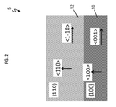
- FIG. 1 is a cross-sectional view of a VFET structure 5 according to one or more embodiments of the present invention.
- the VFET structure 5 depicts both an NFET device 150 and PFET device 152 which have different channel surface orientations and different channel transport directions.
- the NFET 150 has a channel transport direction ⁇ 100> and a channel surface orientation ⁇ 001 ⁇ . In the NFET device 150 , the ⁇ 001 ⁇ surface orientation favors electron mobility.
- the PFET 152 has a channel transport direction ⁇ 110> and a channel surface orientation ⁇ 1-10 ⁇ .
- the channel transport direction ⁇ 110> is the direction that holes (i.e., which are the majority carrier in PFETs) travel between the source and drain (e.g., between source/drain 62 A and source/drain 62 C).
- the ⁇ 110> orientation for the channel transport direction with ⁇ 110 ⁇ or ⁇ 1-10 ⁇ family surfaces provides the highest mobility for holes.
- the VFET structure 5 is a semiconductor device.
- the VFET structure 5 includes a first semiconductor substrate 10 and a second semiconductor substrate 12 .
- the first substrate 10 and the second substrate 12 can be two wafers.
- one or both of the semiconductor substrates 10 and 12 can be a bulk semiconductor substrate.
- a “bulk semiconductor substrate” is a substrate that is composed of a single semiconductor material.
- the semiconductor material that provides the bulk semiconductor substrate can be a semiconducting material including, but not limited to silicon, strained silicon, a silicon carbon alloy (SiC), silicon germanium (SiGe), a silicon germanium and carbon alloy (SiGeC), silicon alloys, germanium, germanium alloys, gallium arsenic, indium arsenic, indium phosphide, as well as other III-V and II-VI compound semiconductors.
- silicon silicon carbon alloy
- SiGe silicon germanium
- SiGeC silicon germanium and carbon alloy
- silicon alloys germanium, germanium alloys, gallium arsenic, indium arsenic, indium phosphide, as well as other III-V and II-VI compound semiconductors.
- the upper surface of the semiconductor substrate 10 and 12 are crystalline material, such as a single crystal material.
- crystalline includes nanocrystalline, polycrystalline or microcrystalline.
- single crystalline denotes a crystalline solid, in which the crystal lattice of the entire sample is substantially continuous and substantially unbroken to the edges of the sample, with substantially no grain boundaries.
- the VFET structure 5 includes isolation regions 14 which are also referred to as shallow trench isolation regions.
- the isolation regions 14 can be composed of any dielectric, such as an oxide, nitride, and/or oxynitride material.
- the isolation region 14 when composed of an oxide can be silicon oxide (SiO 2 )
- the isolation region 14 when composed of a nitride can be silicon nitride.
- the isolation region 14 can be formed using photolithography, etch, and deposition processes.
- the NFET device 150 has a source/drain 52 A, vertical fins 52 B, and source/drain 52 C.
- the PFET device 152 has a source/drain 62 A, vertical fins 62 B, and source/drain 62 C.
- a first spacer 15 is adjacent to the semiconductor substrate 10 , the semiconductor substrate 12 , and isolation regions 14 .
- a high-k dielectric layer 16 is adjacent to the substrate 10 , substrate 12 , isolation regions 14 , fins 52 B, and fins 62 B.
- a gate metal 18 is adjacent to the high-k dielectric layer 16 , first spacer 15 , and second spacer 20 .
- An inter-level dielectric layer 66 is adjacent to the second spacer 20 source/drain 52 C, source/drain 62 C, and contacts 70 , 72 , 74 , 76 , and 78 .
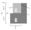
- FIGS. 2-20 illustrate an example process flow of fabricating the VFET structure 5 in FIG. 1 .
- FIG. 2 is a cross-sectional view of the VFET structure 5 depicting a (110) semiconductor substrate 12 on top of a (100) semiconductor substrate 10 (or vice versa) according to one or more embodiments.
- the example shown in FIG. 2 has a (100) bottom substrate 10 and a (110) top substrate 12 , which can be formed by, for example, a wafer bonding technique.
- the orientation of the semiconductor substrate 10 is designed such that the NFETs have (001) channel surface orientation and ⁇ 100> channel transport direction.
- the orientation of the semiconductor substrate 12 is designed such that the PFETs have (1-10) surface orientation and ⁇ 110> channel transport direction.
- FIG. 3 is a cross-sectional view of the VFET structure 5 depicting etching of the semiconductor substrate 10 according to one or more embodiments.
- a mask layer 302 is formed on the PFET side of the VFET structure 5 to protect a portion of the substrate 12 .
- the mask layer 302 can be, for example, a SiNx hard mask.
- Etching is performed to remove part of the semiconductor substrates 10 and 12 thereby forming a via 300 .
- a reactive ion etch (RIE) can be performed to etch down the left side using the SiNx mask to protect the right side and the etching continues until the bottom substrate 10 is reached.
- RIE reactive ion etch
- the etching leaves the semiconductor substrate 10 on the right side (PFET side) higher than the semiconductor substrate 10 on the left side (NFET side), thereby ensuring that the bottom substrate 10 is reached.
- the height of the semiconductor substrate 10 on the side of the NFET device 150 is higher in the y-axis than the height of the semiconductor substrate 10 on the side of the PFET device 152 in FIG. 3 .
- the height of left and right sides of the semiconductor substrate 10 can be about the same.
- FIG. 4 is a cross-sectional view of the VFET structure 5 depicting formation of a side wall spacer 402 according to one or more embodiments.
- the side wall spacer 402 is formed along the side of mask layer 302 , the protected substrate 12 , and a portion of the substrate 10 .
- the side wall spacer 402 can be a SiO 2 side wall spacer.
- the side wall spacer 402 can be formed by conformal deposition of the side wall material and followed by a directional etch back.
- FIG. 5 is a cross-sectional view of the VFET structure 5 depicting epitaxial growth of the semiconductor substrate 10 according to one or more embodiments.
- An epitaxial layer 502 is epitaxially grown on exposed (100) surface of the semiconductor substrate 10 on the NFET 150 . Accordingly, both the semiconductor substrate 10 and the epitaxial layer 502 have the same surface orientation (100). It should be appreciated that n-type dopants can be included during the epitaxial growth of the epitaxial layer 502 (also referred to as an epi layer).
- the semiconductor substrate 12 is protected by the mask layer 302 and the side wall spacer 402 .
- epitaxially growing, epitaxial growth and/or deposition mean the growth of a semiconductor material on a deposition surface of a semiconductor material, in which the semiconductor material being grown has the same crystalline characteristics as the semiconductor material of the deposition surface.
- the depositing atoms arrive at the deposition surface with sufficient energy to move around on the surface and orient themselves to the crystal arrangement of the atoms of the deposition surface.
- an epitaxial film deposited on a ⁇ 100> crystal surface will take on a ⁇ 100> orientation.
- the exposed upper surface of the semiconductor substrate 10 provides the seed surface for epitaxial growth of the semiconductor material of the epitaxial layer 502 . More specifically, epitaxial growth of the semiconductor material of the epitaxial layer 502 starts at the exposed upper surface of the semiconductor substrate 10 filling the via 300 (shown in FIG. 3 ) as the deposition process continues, and once the via 300 is filled, the epitaxially grown epitaxial layer 502 grows from the via 300 . As the epitaxially growth process continues, the semiconductor material can fill the via 300 , where the epitaxial semiconductor material is in direct contact with the base surface (of the substrate 10 ) and the side wall spacer 402 . In some embodiments, the epitaxial growth can continue after the via 300 is entirely filled and until a portion of the epitaxial semiconductor material of the epitaxial layer 502 extends from the via 300 as shown in FIG. 6 .
- FIG. 6 is a cross-sectional view of the VFET structure 5 depicting planarization according to one or more embodiments.
- the top of the VFET structure 5 is planarized to remove the excess semiconductor material of the epitaxial layer 502 .
- the semiconductor material of the epitaxial layer 502 can be removed by, for example, a suitable etching process, grinding, or chemical mechanical polishing (CMP).
- CMP chemical mechanical polishing
- the upper surface of the VFET structure 5 can be planarized so that the upper surface of the epitaxial layer 502 is coplanar with the upper surface of the substrate 12 . Also, the top surface of the VFET structure 5 can be cleaned.
- FIG. 7 is a cross-sectional view of the VFET structure 5 depicting formation of the vertical fin channels according to one or more embodiments.
- a fin mask layer 702 can be deposited on top of the VFET structure 5 and patterned on top of the epitaxial layer 502 and the semiconductor substrate 12 .
- the fin mask layer 702 is a hard mask.
- the patterned fin mask layer 702 is in preparation of forming the fins 52 B and fins 62 B of the NFET device 150 and PFET device 152 respectively. With the fin mask layer 702 in place, etching is performed to form the vertical fins 52 B in the epitaxial layer 502 of the NFET device 150 and form the vertical fins 62 B in the semiconductor substrate 12 of the PFET device 152 .
- the etching results in formation of the source/drain 52 A of the NFET device 150 and the source/drain 62 A of the PFET device 152 .
- the side wall spacer 402 is also recessed along with the epitaxial layer 502 and the semiconductor substrate 12 .
- FIG. 8 is a cross-sectional view of the VFET structure 5 depicting formation of a protective layer according to one or more embodiments.
- the protective layer 802 is formed over the fin mask layer 702 , vertical fins 52 B, vertical fins 62 B, the source/drain 52 A, and the source/drain 62 A.
- the protective layer 802 can be an organic planarizing layer (OPL) that protects the covered parts.
- OPL organic planarizing layer
- the protective layer 802 can be patterned to form voids 806 in the protective layer 802 such that open areas exposed on sides of the fins 52 B and 62 B. Accordingly, portions of the source/drain 52 A, the source/drain 62 A, and the side wall spacer 402 are exposed in the open areas 806 in preparation for etching.
- the protective layer 802 can be patterned using lithography.
- FIG. 9 is a cross-sectional view of the VFET structure 5 depicting trench formation according to one or more embodiments.
- trenches 902 can be formed at the exposed portions 806 (in FIG. 8 ) of the source/drain 52 A, the source/drain 62 A, and the side wall spacer 402 discussed in FIG. 8 .
- the trenches 902 remove the side wall spacer 402 .
- FIG. 10 is a cross-sectional view of the VFET structure 5 depicting formation of a fill layer according to one or more embodiments.
- a fill layer 1002 is formed on top of the VFET structure 5 to fill in the trenches 902 .
- the fill layer 1002 can be, for example, SiO 2 .
- the fill layer 1002 can be planarized, for example CMP, down to the fin mask layer 702 , such that the top surfaces of the fin mask layer 702 and the fill layer 1002 are coplanar.
- FIG. 11 is a cross-sectional view of the VFET structure 5 depicting formation of the isolation regions 14 according to one or more embodiments.
- the material of fill layer 1002 is etched back to form the isolation regions 14 in the trenches 902 (shown in FIG. 9 ).
- the fill layer 1002 is etched back to a height lower than the source/drain 52 A and source/drain 62 A in the y-axis.
- the isolation regions 14 can be SiO 2 , and the SiO 2 material is a lower height in the isolations regions 14 in preparation to later form the gate.
- the fill layer 1002 can be etched back using a selective etch process.
- FIG. 12 is a cross-sectional view of the VFET structure 5 depicting formation of the high-k dielectric material according to one or more embodiments.
- a bottom/first spacer 15 is formed on top of the source/drain 52 A, the source/drain 62 A, the isolation regions 14 , and the fin mask layers 702 .
- a direction deposition technique can be utilized to deposit the bottom/first spacer 15 .
- the bottom/first spacer 15 can be a low-k dielectric material. The description of the bottom/first spacer 15 also applies to the top/second spacer 20 .
- a high-k dielectric material 16 is formed on top of the VFET structure 5 .
- the high-k dielectric material 16 is formed to cover the bottom/first spacer 15 (along with the portions of the bottom/first spacer 15 on top of the fin mask layers 702 ), the vertical fins 52 B, the vertical fins 62 B, and the fin mask layers 702 .
- the high-k dielectric material 16 can be a dielectric material having a dielectric constant greater than 3.9, 7.0, or 10.0.
- suitable materials for the high-k dielectric material 16 can include oxides, nitrides, oxynitrides, silicates (e.g., metal silicates), aluminates, titanates, nitrides, or any combination thereof.
- high-k materials include, but are not limited to, metal oxides such as hafnium oxide, hafnium silicon oxide, hafnium silicon oxynitride, lanthanum oxide, lanthanum aluminum oxide, zirconium oxide, zirconium silicon oxide, zirconium silicon oxynitride, tantalum oxide, titanium oxide, barium strontium titanium oxide, barium titanium oxide, strontium titanium oxide, yttrium oxide, aluminum oxide, lead scandium tantalum oxide, and lead zinc niobate.
- the high-k material can further include dopants such as, for example, lanthanum and aluminum.
- the high-k dielectric material can be formed by suitable deposition processes, for example, chemical vapor deposition (CVD), plasma-enhanced chemical vapor deposition (PECVD), atomic layer deposition (ALD), evaporation, physical vapor deposition (PVD), chemical solution deposition, or other like processes.
- CVD chemical vapor deposition
- PECVD plasma-enhanced chemical vapor deposition
- ALD atomic layer deposition
- evaporation evaporation
- PVD physical vapor deposition
- chemical solution deposition evapor deposition
- the thickness of the dielectric material can vary depending on the deposition process as well as the composition and number of high-k dielectric materials used.
- the bottom/first spacer 15 (and/or the top/second spacer 20 ) can be composed of, for example, an oxide, nitride or oxynitride material layer.
- the bottom/first spacer 15 can be composed of silicon oxide (SiO 2 ).
- the term “low-k” denotes a dielectric constant less than 3.9.
- the low-k dielectric material of the bottom/first spacer 15 has a dielectric constant ranging from 1.0 to 3.0.
- the bottom/first spacer 15 includes SiCOH or an aromatic hydrocarbon polymer composition, such as SILKTM.
- the bottom/first spacer 15 can include carbon-doped oxides. In other embodiments, the bottom/first spacer 15 can include an undoped silica glass. In other embodiments, the bottom/first spacer 15 can include be composed of diamond-like carbon (DLC).
- DLC diamond-like carbon
- the deposition process for forming the bottom/first spacer 15 (and/or the top/second spacer 20 ) can include chemical vapor deposition (CVD), plasma enhanced chemical vapor deposition (PECVD), physical vapor deposition (PVD), high-density plasma CVD or spin-on glass process.
- CVD chemical vapor deposition
- PECVD plasma enhanced chemical vapor deposition
- PVD physical vapor deposition
- high-density plasma CVD or spin-on glass process.
- FIG. 13 is a cross-sectional view of the VFET structure 5 depicting formation of a gate material according to one or more embodiments.
- the gate material fills voids around the fins 52 B and the fins 62 B, and the gate material is utilized to form a gate metal 18 in FIG. 14 .
- the gate material is planarized to make the top of the fins 52 B and fins 62 B, particularly the bottom/first spacer 15 on top of fins 52 B and 62 B, coplanar with the gate material 18 .
- FIG. 14 is a cross-sectional view of the VFET structure 5 depicting etching of the gate material according to one or more embodiments.
- a gate metal recess etch is performed to recess the gate material to the desired height for the gate metal 18 .
- the gate material of the gate metal 18 includes one or more work function metals.
- the type of work function metal(s) can depend on the type of transistor and can differ between the NFET and PFET devices.
- suitable work function metals include p-type work function metal materials and n-type work function metal materials.
- P-type work function materials include compositions such as ruthenium, palladium, platinum, cobalt, nickel, and conductive metal oxides, or any combination thereof.
- N-type metal materials include compositions such as hafnium, zirconium, titanium, tantalum, aluminum, metal carbides (e.g., hafnium carbide, zirconium carbide, titanium carbide, and aluminum carbide), aluminides, or any combination thereof.
- the work function metal(s) can be deposited by a suitable deposition process, for example, CVD, PECVD, PVD, plating, thermal or e-beam evaporation, and sputtering.
- FIG. 15 is a cross-sectional view of the VFET structure 5 depicting top/second spacer formation according to one or more embodiments.
- the top/second spacer 20 is formed on top of the gate metal 18 , the high-k material 16 , and the bottom/first spacer 15 that is on the fin mask layers 702 .
- a direction deposition technique can be utilized to deposit the top/second spacer 20 .
- the top/second spacer 20 can be a low-k dielectric material, and reference can be made to the bottom/first spacer 15 for the description of the top/second spacer 20 .
- the gate metal 18 and the high-k dielectric material 16 are referred to as a gate stack.
- FIG. 16 is a cross-sectional view of the VFET structure 5 depicting formation of the inter-level dielectric (ILD) layer 66 according to one or more embodiments.
- the ILD 66 is deposited on top of the VFET structure 5 and is planarized (e.g., CMP) down to the fin mask layer 702 , such that the top surface of ILD 66 is coplanar with the top surface of the fin mask layer 702 .
- the ILD 66 can be SiO 2 .
- FIG. 17 is a cross-sectional view of the VFET structure 5 depicting exposure of vertical fins 52 B in the ILD 66 according to one or more embodiments.
- Lithography is utilized to etch an opening 1702 in the ILD 66 to expose the vertical fins 52 B of the NFET device 150 and remove the fin mask layer 702 on the fins 52 B.
- the PFET side is blocked, for example, using a mask (not shown) when etching the opening 1702 .
- FIG. 18 is a cross-sectional view of the VFET structure 5 depicting formation of the top source/drain 52 C according to one or more embodiments.
- the top source/drain 52 C is epitaxially grown from the fins 52 B of the NFET device 150 .
- the top source/drain 52 C is epitaxially grown with the same crystalline structure of both the fins 52 B and substrate 10 .
- the material of the source/drain 52 C, vertical fins 52 B, and source/drain 52 A can be the same material.
- the material of the source/drain 52 C, vertical fins 52 B, and source/drain 52 A can be the same as the substrate 10 , with the addition of n-type dopants.
- FIG. 19 is a cross-sectional view of the VFET structure 5 depicting exposure of vertical fins 62 B in the ILD 66 according to one or more embodiments.
- Lithography is utilized to etch an opening 1902 in the ILD 66 to expose the fins 62 B of the PFET device 152 and remove the fin mask layer 702 on the vertical fins 62 B.
- the NFET side is blocked, for example, using a mask (not shown) when etching the opening 1902 .
- FIG. 20 is a cross-sectional view of the VFET structure 5 depicting formation of the top source/drain 62 C according to one or more embodiments.
- the top source/drain 62 C is epitaxially grown from the fins 62 B of the PFET device 150 .
- the top source/drain 62 C is epitaxially grown with the same crystalline structure of both the fins 62 B and substrate 12 .
- the material of the source/drain 62 C, vertical fins 62 B, and source/drain 62 A can be the same material.
- the material of the source/drain 62 C, vertical fins 62 B, and source/drain 62 A can be the same as the substrate 10 , with the addition of p-type dopants.
- FIG. 1 is a cross-sectional view of the final version of the VFET structure 5 .
- additional material of the ILD 66 is deposited over the epitaxially grown top source/drain 52 C and the epitaxially grown top source/drain 62 C.
- contacts 70 , 72 , 74 , 76 , and 78 are formed in the ILD 66 .
- the source/drain contact 70 is on the bottom source/drain 52 A and the source/drain contact 72 is on the top source/drain 52 C.
- the source/drain contact 76 is on the top source/drain 62 C and the source/drain contact 78 is on the bottom/source drain 62 A.
- the gate contact 74 is on the gate metal 18 .
- FIG. 21 is a flow chart 2100 of a method of forming a vertical device 5 according to one or more embodiments. Reference can be made to FIGS. 1-20 .
- a first substrate 10 adjacent to a second substrate 12 , where the first substrate has a first surface orientation, where the second substrate 12 has a second surface orientation different from the first surface orientation.
- an NFET device 150 is formed with the first substrate 10 , where the NFET device 150 includes a first source (e.g., source/drain) 52 A, a first drain (e.g., source/drain) 52 C, and one or more first fins 52 B, where the first source 52 A and the first drain 52 C have a vertical relationship with respect to the one or more first fins 52 B.
- a first source e.g., source/drain
- a first drain e.g., source/drain
- a PFET device 152 is formed with the second substrate 12 , where the PFET device 152 includes a second source 62 A, a second drain 62 C, and one or more second fins 62 B, where the second source 62 A and the second drain 62 C have a vertical relationship with respect to the one or more second fins 62 B.
- the first source 52 A, the first drain 52 C, and the one or more first fins 52 B have the first surface orientation as the first substrate 10 .
- the second source 62 A, the second drain 62 C, and the one or more second fins 62 B have the second surface orientation as the second substrate 12 .
- the first one or more fins 52 B have a first channel transport direction and the second one or more fins 62 B have a second channel transport direction, where the first channel transport direction is different from the second channel transport direction.
- the first channel transport direction is defined for mobility of electrons (as the majority carrier) and the second channel transport direction is defined for mobility of holes (as the majority carrier).
- the first channel transport direction is different from the first surface orientation.
- the second channel transport direction is different from the second surface orientation.
- the first transport direction is ⁇ 100> and the second transport direction is ⁇ 110>.
- the first surface orientation is ⁇ 001>.
- the second surface orientation is ⁇ 1-10>.
- microelectronic device fabrication methods can be utilized to fabricate the components/elements discussed herein as understood by one skilled in the art.
- semiconductor device fabrication the various processing steps fall into four general categories: deposition, removal, patterning, and modification of electrical properties.
- Deposition is any process that grows, coats, or otherwise transfers a material onto the wafer.
- Available technologies include physical vapor deposition (PVD), chemical vapor deposition (CVD), electrochemical deposition (ECD), molecular beam epitaxy (MBE) and more recently, atomic layer deposition (ALD) among others.
- the terms “epitaxially growing, epitaxial growth and/or deposition” mean the growth of a semiconductor material on a deposition surface of a semiconductor material, in which the semiconductor material being grown has the same crystalline characteristics as the semiconductor material of the deposition surface.
- the depositing atoms arrive at the deposition surface with sufficient energy to move around on the surface and orient themselves to the crystal arrangement of the atoms of the deposition surface.
- an epitaxial film deposited on a ⁇ 100 ⁇ crystal surface will take on a ⁇ 100 ⁇ orientation.
- Removal is any process that removes material from the wafer: examples include etch processes (either wet or dry), and chemical-mechanical planarization (CMP), etc.
- selective in reference to a material removal process denotes that the rate of material removal for a first material is greater than the rate of removal for at least another material of the structure to which the material removal process is being applied.
- a selective etch can include an etch chemistry that removes a first material selectively to a second material by a ratio of 100:1 or greater, e.g., 1000:1.
- Patterning is the shaping or altering of deposited materials, and is generally referred to as lithography.
- the wafer is coated with a chemical called a photoresist; then, a machine called a stepper focuses, aligns, and moves a mask, exposing select portions of the wafer below to short wavelength light; the exposed regions are washed away by a developer solution. After etching or other processing, the remaining photoresist is removed.
- Patterning also includes electron-beam lithography.
- Modification of electrical properties can include doping, such as doping transistor sources and drains, generally by diffusion and/or by ion implantation. These doping processes are followed by furnace annealing or by rapid thermal annealing (RTA). Annealing serves to activate the implanted dopants.
- doping such as doping transistor sources and drains
- RTA rapid thermal annealing
Abstract
Description
Claims (19)
Priority Applications (1)
Application Number | Priority Date | Filing Date | Title |
---|---|---|---|
US15/436,013 US10177046B2 (en) | 2017-02-17 | 2017-02-17 | Vertical FET with different channel orientations for NFET and PFET |
Applications Claiming Priority (1)
Application Number | Priority Date | Filing Date | Title |
---|---|---|---|
US15/436,013 US10177046B2 (en) | 2017-02-17 | 2017-02-17 | Vertical FET with different channel orientations for NFET and PFET |
Publications (2)
Publication Number | Publication Date |
---|---|
US20180240716A1 US20180240716A1 (en) | 2018-08-23 |
US10177046B2 true US10177046B2 (en) | 2019-01-08 |
Family
ID=63167974
Family Applications (1)
Application Number | Title | Priority Date | Filing Date |
---|---|---|---|
US15/436,013 Expired - Fee Related US10177046B2 (en) | 2017-02-17 | 2017-02-17 | Vertical FET with different channel orientations for NFET and PFET |
Country Status (1)
Country | Link |
---|---|
US (1) | US10177046B2 (en) |
Cited By (2)
Publication number | Priority date | Publication date | Assignee | Title |
---|---|---|---|---|
US11037905B2 (en) | 2019-04-26 | 2021-06-15 | International Business Machines Corporation | Formation of stacked vertical transport field effect transistors |
US11615990B2 (en) | 2020-03-24 | 2023-03-28 | International Business Machines Corporation | CMOS top source/drain region doping and epitaxial growth for a vertical field effect transistor |
Families Citing this family (2)
Publication number | Priority date | Publication date | Assignee | Title |
---|---|---|---|---|
US10269803B2 (en) * | 2017-08-31 | 2019-04-23 | Taiwan Semiconductor Manufacturing Company, Ltd. | Hybrid scheme for improved performance for P-type and N-type FinFETs |
US10833079B2 (en) | 2019-01-02 | 2020-11-10 | International Business Machines Corporation | Dual transport orientation for stacked vertical transport field-effect transistors |
Citations (13)
Publication number | Priority date | Publication date | Assignee | Title |
---|---|---|---|---|
US7432149B2 (en) | 2005-06-23 | 2008-10-07 | Taiwan Semiconductor Manufacturing Company, Ltd. | CMOS on SOI substrates with hybrid crystal orientations |
US7485506B2 (en) | 2004-06-21 | 2009-02-03 | International Business Machines Corporation | Hybrid substrate technology for high-mobility planar and multiple-gate MOSFETS |
US7569857B2 (en) | 2006-09-29 | 2009-08-04 | Intel Corporation | Dual crystal orientation circuit devices on the same substrate |
US7892956B2 (en) | 2007-09-24 | 2011-02-22 | International Business Machines Corporation | Methods of manufacture of vertical nanowire FET devices |
US20140217467A1 (en) * | 2013-02-04 | 2014-08-07 | Globalfoundries Inc. | Methods of forming substrates comprised of different semiconductor materials and the resulting device |
US20150014789A1 (en) | 2007-06-18 | 2015-01-15 | Texas Instruments Incorporated | Integrated circuits with aligned (100) nmos and (110) pmos finfet sidewall channels |
US20150303202A1 (en) * | 2011-06-16 | 2015-10-22 | Min-chul Sun | Semiconductor devices having vertical device and non-vertical device and methods of forming the same |
US20160163810A1 (en) * | 2014-12-04 | 2016-06-09 | Taiwan Semiconductor Manufacturing Co., Ltd | Gate all around device structure and fin field effect transistor (finfet) device structure |
US20170076993A1 (en) * | 2015-09-04 | 2017-03-16 | International Business Machines Corporation | Self-aligned punch through stopper liner for bulk finfet |
US9601491B1 (en) * | 2016-01-28 | 2017-03-21 | International Business Machines Corporation | Vertical field effect transistors having epitaxial fin channel with spacers below gate structure |
US9653602B1 (en) * | 2016-03-21 | 2017-05-16 | International Business Machines Corporation | Tensile and compressive fins for vertical field effect transistors |
US20170154821A1 (en) * | 2015-11-30 | 2017-06-01 | International Business Machines Corporation | Semiconductor device including finfet and fin varactor |
US20180005899A1 (en) * | 2016-06-30 | 2018-01-04 | International Business Machines Corporation | Fabrication of a vertical fin field effect transistor with reduced dimensional variations |
-
2017
- 2017-02-17 US US15/436,013 patent/US10177046B2/en not_active Expired - Fee Related
Patent Citations (14)
Publication number | Priority date | Publication date | Assignee | Title |
---|---|---|---|---|
US7485506B2 (en) | 2004-06-21 | 2009-02-03 | International Business Machines Corporation | Hybrid substrate technology for high-mobility planar and multiple-gate MOSFETS |
US7432149B2 (en) | 2005-06-23 | 2008-10-07 | Taiwan Semiconductor Manufacturing Company, Ltd. | CMOS on SOI substrates with hybrid crystal orientations |
US7569857B2 (en) | 2006-09-29 | 2009-08-04 | Intel Corporation | Dual crystal orientation circuit devices on the same substrate |
US20150014789A1 (en) | 2007-06-18 | 2015-01-15 | Texas Instruments Incorporated | Integrated circuits with aligned (100) nmos and (110) pmos finfet sidewall channels |
US7892956B2 (en) | 2007-09-24 | 2011-02-22 | International Business Machines Corporation | Methods of manufacture of vertical nanowire FET devices |
US20150303202A1 (en) * | 2011-06-16 | 2015-10-22 | Min-chul Sun | Semiconductor devices having vertical device and non-vertical device and methods of forming the same |
US20140217467A1 (en) * | 2013-02-04 | 2014-08-07 | Globalfoundries Inc. | Methods of forming substrates comprised of different semiconductor materials and the resulting device |
US20160163810A1 (en) * | 2014-12-04 | 2016-06-09 | Taiwan Semiconductor Manufacturing Co., Ltd | Gate all around device structure and fin field effect transistor (finfet) device structure |
US20170076993A1 (en) * | 2015-09-04 | 2017-03-16 | International Business Machines Corporation | Self-aligned punch through stopper liner for bulk finfet |
US20170154821A1 (en) * | 2015-11-30 | 2017-06-01 | International Business Machines Corporation | Semiconductor device including finfet and fin varactor |
US9601491B1 (en) * | 2016-01-28 | 2017-03-21 | International Business Machines Corporation | Vertical field effect transistors having epitaxial fin channel with spacers below gate structure |
US20170222021A1 (en) * | 2016-01-28 | 2017-08-03 | International Business Machines Corporation | Vertical field effect transistors with protective fin liner during bottom spacer recess etch |
US9653602B1 (en) * | 2016-03-21 | 2017-05-16 | International Business Machines Corporation | Tensile and compressive fins for vertical field effect transistors |
US20180005899A1 (en) * | 2016-06-30 | 2018-01-04 | International Business Machines Corporation | Fabrication of a vertical fin field effect transistor with reduced dimensional variations |
Non-Patent Citations (1)
Title |
---|
M. Yang et al., "Performance Dependence of CMOS on Silicon Substrate Orientation for Ultrathin Oxynitride and HfO2 Gate Dielectrics," IEEE Electron Device Letters, vol. 24, No. 5, May 2003, pp. 339-341. |
Cited By (2)
Publication number | Priority date | Publication date | Assignee | Title |
---|---|---|---|---|
US11037905B2 (en) | 2019-04-26 | 2021-06-15 | International Business Machines Corporation | Formation of stacked vertical transport field effect transistors |
US11615990B2 (en) | 2020-03-24 | 2023-03-28 | International Business Machines Corporation | CMOS top source/drain region doping and epitaxial growth for a vertical field effect transistor |
Also Published As
Publication number | Publication date |
---|---|
US20180240716A1 (en) | 2018-08-23 |
Similar Documents
Publication | Publication Date | Title |
---|---|---|
US10930563B2 (en) | Formation of stacked nanosheet semiconductor devices | |
US10312147B2 (en) | Multi-layer work function metal gates with similar gate thickness to achieve multi-VT for VFETs | |
US11705517B2 (en) | Nanosheet transistors with strained channel regions | |
US10896972B2 (en) | Self-aligned contact for vertical field effect transistor | |
US10896851B2 (en) | Vertically stacked transistors | |
KR20200007711A (en) | High performance mosfet | |
US10177046B2 (en) | Vertical FET with different channel orientations for NFET and PFET | |
US10014377B2 (en) | III-V field effect transistor on a dielectric layer | |
CN110637367B (en) | Ultra-long channel device within VFET architecture | |
US10002925B2 (en) | Strained semiconductor device | |
US10573745B2 (en) | Super long channel device within VFET architecture | |
US10461184B1 (en) | Transistor having reduced gate-induced drain-leakage current | |
US10115824B2 (en) | Forming a contact for a semiconductor device | |
US11876124B2 (en) | Vertical transistor having an oxygen-blocking layer | |
US10665694B2 (en) | Vertical transistors having improved gate length control | |
US10811508B2 (en) | Vertical transistors having multiple gate thicknesses for optimizing performance and device density |
Legal Events
Date | Code | Title | Description |
---|---|---|---|
AS | Assignment |
Owner name: INTERNATIONAL BUSINESS MACHINES CORPORATION, NEW Y Free format text: ASSIGNMENT OF ASSIGNORS INTEREST;ASSIGNORS:CHENG, KANGGUO;MIAO, XIN;XU, WENYU;AND OTHERS;REEL/FRAME:041287/0752 Effective date: 20170125 |
|
STCF | Information on status: patent grant |
Free format text: PATENTED CASE |
|
AS | Assignment |
Owner name: ELPIS TECHNOLOGIES INC., CANADA Free format text: ASSIGNMENT OF ASSIGNORS INTEREST;ASSIGNOR:INTERNATIONAL BUSINESS MACHINES CORPORATION;REEL/FRAME:052644/0868 Effective date: 20200306 |
|
FEPP | Fee payment procedure |
Free format text: MAINTENANCE FEE REMINDER MAILED (ORIGINAL EVENT CODE: REM.); ENTITY STATUS OF PATENT OWNER: LARGE ENTITY |
|
LAPS | Lapse for failure to pay maintenance fees |
Free format text: PATENT EXPIRED FOR FAILURE TO PAY MAINTENANCE FEES (ORIGINAL EVENT CODE: EXP.); ENTITY STATUS OF PATENT OWNER: LARGE ENTITY |
|
STCH | Information on status: patent discontinuation |
Free format text: PATENT EXPIRED DUE TO NONPAYMENT OF MAINTENANCE FEES UNDER 37 CFR 1.362 |
|
FP | Lapsed due to failure to pay maintenance fee |
Effective date: 20230108 |