US10171088B1 - Quantum circuit for shifting phase of target qubit based on control qubit - Google Patents
Quantum circuit for shifting phase of target qubit based on control qubit Download PDFInfo
- Publication number
- US10171088B1 US10171088B1 US16/034,073 US201816034073A US10171088B1 US 10171088 B1 US10171088 B1 US 10171088B1 US 201816034073 A US201816034073 A US 201816034073A US 10171088 B1 US10171088 B1 US 10171088B1
- Authority
- US
- United States
- Prior art keywords
- qubit
- gate
- cnot
- state
- converted
- Prior art date
- Legal status (The legal status is an assumption and is not a legal conclusion. Google has not performed a legal analysis and makes no representation as to the accuracy of the status listed.)
- Active
Links
Images
Classifications
-
- H—ELECTRICITY
- H03—ELECTRONIC CIRCUITRY
- H03K—PULSE TECHNIQUE
- H03K19/00—Logic circuits, i.e. having at least two inputs acting on one output; Inverting circuits
- H03K19/02—Logic circuits, i.e. having at least two inputs acting on one output; Inverting circuits using specified components
- H03K19/195—Logic circuits, i.e. having at least two inputs acting on one output; Inverting circuits using specified components using superconductive devices
-
- G—PHYSICS
- G06—COMPUTING; CALCULATING OR COUNTING
- G06N—COMPUTING ARRANGEMENTS BASED ON SPECIFIC COMPUTATIONAL MODELS
- G06N10/00—Quantum computing, i.e. information processing based on quantum-mechanical phenomena
-
- G—PHYSICS
- G06—COMPUTING; CALCULATING OR COUNTING
- G06N—COMPUTING ARRANGEMENTS BASED ON SPECIFIC COMPUTATIONAL MODELS
- G06N20/00—Machine learning
-
- G06N99/002—
-
- H—ELECTRICITY
- H03—ELECTRONIC CIRCUITRY
- H03K—PULSE TECHNIQUE
- H03K19/00—Logic circuits, i.e. having at least two inputs acting on one output; Inverting circuits
- H03K19/20—Logic circuits, i.e. having at least two inputs acting on one output; Inverting circuits characterised by logic function, e.g. AND, OR, NOR, NOT circuits
Definitions
- the present disclosure relates to quantum computing, and more particularly to a quantum circuit for shifting the phase of a target qubit based on a control qubit.
- a quantum computer performs calculation based on the qubits represented by the superposition of ‘0’ and ‘1’, so that it may have a much higher calculation speed than a digital computer using bits represented by only ‘0’ or ‘1’.
- any arbitrary single-qubit gate or Z-rotation gate may be implemented with relatively high accuracy.
- calculation of a fault-tolerant scheme which guarantees an arbitrary probability of success is required.
- the operation of all quantum algorithms should be expressed by a universal set proposed from the fault tolerant protocol.
- a Controlled-Rn gate which shifts the phase of the target qubits based on the control qubits, receives attention in that it constitutes a key part of many other quantum computations such as Quantum Fourier Transform (QFT).
- QFT Quantum Fourier Transform
- the decomposition of the Controlled-Rn gate is important in the overall part of the quantum algorithm, and there is a need to reduce the number of gates during the decomposition of the Controlled-Rn gate.
- the present disclosure is to provide a quantum circuit capable of reducing the number of basic gates included in the controlled-rotation gate that shifts the phase of the target qubit based on the control qubits and reducing the operation time of the quantum computing.
- An embodiment of the inventive concept provides a quantum circuit according to an embodiment of the inventive concept shifts the phase of the target qubit by ⁇ /2 n ⁇ 1 based on the control qubit.
- the quantum circuit includes a first auxiliary circuit configured to convert a first qubit state according to an entanglement of the control qubit, the target qubit, and an ancillary qubit having a
- the first auxiliary circuit determines a
- the second auxiliary circuit determines a
- the first auxiliary circuit and the second auxiliary circuit may be the same.
- the first auxiliary circuit may determine the
- the second auxiliary circuit may determine the
- each of the first and second auxiliary circuits may include two Hadamard gates, four T-gates, and four CNOT gates.
- Each of the first auxiliary circuit and the second auxiliary circuit may operate in a total of eight operations.
- Each of the first auxiliary circuit and the second auxiliary circuit may perform
- the first auxiliary circuit and the second auxiliary circuit may be Hermitian to each other.
- the first auxiliary circuit may determine the
- each of the first and second auxiliary circuits may include two Hadamard gates, four T-gates, and six CNOT gates.
- Each of the first auxiliary circuit and the second auxiliary circuit may operate in a total of ten operations.
- the first auxiliary circuit performs
- the second auxiliary circuit performs
- a quantum circuit includes a first CNOT gate configured to perform a CNOT calculation on an ancillary qubit having a
- FIG. 1 is a view for explaining a controlled-rotation gate included in a quantum circuit to be implemented in an embodiment of an inventive concept
- FIG. 2 is a view for explaining an embodiment using an ancillary qubit for the implementation of a controlled-rotation gate
- FIG. 3 is a circuit diagram of decomposing the controlled-swap gate of FIG. 2 into basic gates
- FIG. 4 is a block diagram of a quantum circuit according to an embodiment of the inventive concept
- FIG. 5 is a circuit diagram embodying an embodiment of the quantum circuit of FIG. 4 ;
- FIG. 6 is a circuit diagram embodying an embodiment of the quantum circuit of FIG. 4 ;
- FIG. 7 is a circuit diagram of a quantum circuit according to an embodiment of the inventive concept.
- FIG. 1 is a view for explaining a controlled-rotation gate included in a quantum circuit to be implemented in an embodiment of an inventive concept.
- a quantum circuit 100 includes a controlled-rotation gate 110 , which is a 2-qubit-based gate.
- ⁇ > 101 with a 2-qubit state is inputted to the quantum circuit 100 .
- a logic qubit 101 includes a control qubit and a target qubit. Each of the control qubit and the target qubit may have a single-qubit state.
- the single-qubit state may be expressed as a 0
- 2 1.
- the logic qubit 101 may be expressed as
- ⁇ > a 00
- the controlled-rotation gate 110 shifts the phase of the target qubit by ⁇ /2 n ⁇ 1 based on the state of the control qubit.
- n may be an integer.
- the phase of the target qubit may be shifted by ⁇ /2 n ⁇ 1 . If the control qubit is in the
- the rotation gate Rn and the controlled-rotation gate Controlled-Rn for shifting the phase of the single-qubit are defined as in Equation 1.
- the controlled-rotation gate 110 which is a 2-qubit-based gate, may be decomposed into a quantum circuit 100 ′ including a first rotation gate 120 , a second rotation gate 130 , a first CNOT gate 140 , a third rotation gate 150 , and a second CNOT gate 160 .
- the first to third rotation gates 120 , 130 , and 150 are single-qubit-based gates.
- the first rotation gate 120 may shift the phase of the control qubit by ⁇ /2 n and the second rotation gate 130 may shift the phase of the target qubit by ⁇ /2 n .
- the first CNOT gate 140 may perform a CNOT calculation on the target qubit converted by the second rotation gate 130 based on the control qubit converted by the first rotation gate 120 . For example, if the control qubit is in the
- the CNOT gate that performs the CNOT calculation is defined by Equation 2.
- the third rotation gate 150 may shift the phase of the target qubit converted by the first CNOT gate 140 by ⁇ /2 n .
- the third rotation gate (R ⁇ n+1 ) 150 may be Hermitian with the first rotation gate (R n+1 ) 120 or the second rotation gate (R n+1 ) 130 . That is, the third rotation gate 150 may appear as a complex conjugate of the transpose matrix of the first rotation gate 120 or the second rotation gate 130 .
- the second CNOT gate 160 may perform a CNOT calculation on the target qubit converted by the third rotation gate 150 based on the control qubit converted by the first rotation gate 120 .
- Each of the first through third rotation gates 120 , 130 , and 150 may be approximately decomposed into the basic gates of a universal set. That is, each of the first through third rotation gates 120 , 130 , and 150 may be implemented with a universal set including Hadamard gate (hereinafter referred to as H-gate), ⁇ /8 phase shift gate (hereinafter referred to as T-gate), and Controlled-NOT (CNOT) gate.
- H-gate Hadamard gate
- T-gate ⁇ /8 phase shift gate
- CNOT Controlled-NOT
- the CNOT gate is as shown in Equation 2, and the H-gate and T-gate are defined as shown in Equation 3.
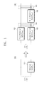
- FIG. 2 is a view for explaining an embodiment using an ancillary qubit for the implementation of a controlled-rotation gate.
- a quantum circuit 200 includes a controlled-rotation gate 210 , which is a 2-qubit-based gate.
- the controlled-rotation gate 210 corresponds to the controlled-rotation gate 110 of FIG. 1 .
- ⁇ > 201 with a 2-qubit state and an ancillary qubit 202 are inputted to the quantum circuit 200 .
- the ancillary qubit 202 may be provided to ensure the efficiency of decomposition of the controlled-rotation gate 210 , and may have the
- the controlled-rotation gate 210 which is a 2-qubit-based gate, may be decomposed into a quantum circuit 200 ′ including a rotation gate 220 , a first controlled-swap gate 240 , and a second controlled-swap gate 260 .
- the rotation gate 220 is a single-qubit-based gate.
- the rotation gate 220 may shift the phase of the target qubit by ⁇ /2 n ⁇ 1 .
- the first controlled-swap gate 240 and the second controlled-swap gate 260 may be a controlled-swap gate that exchanges the target qubit and the ancillary qubit 202 based on the control qubit.
- the first controlled-swap gate 240 exchanges the target qubit and the ancillary qubit 202 based on the control qubit. For example, if the control qubit is in the
- the second controlled-swap gate 260 swaps the ancillary qubit 202 swapped by the first controlled-swap gate 240 with the target qubit converted by the rotation gate 220 , based on the control qubit. That is, the ancillary qubit 202 may be measured in the
- the first controlled-swap gate 240 and the second controlled-swap-gate 260 may substantially have the same configuration.
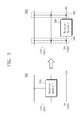
- FIG. 3 is a circuit diagram of decomposing the controlled-swap gate of FIG. 2 into basic gates.
- the controlled-swap gate 240 of FIG. 3 corresponds to the first controlled-swap gate 240 or the second controlled-swap gate 260 of FIG. 2 .
- the controlled-swap gate 240 includes a first CNOT gate 241 , a second CNOT gate 242 , a first H-gate 243 , a first T-gate 244 , a second T-gate (T-gate) 245 , a third T-gate 246 , a third CNOT gate 247 , a fourth CNOT gate 248 , a fourth T-gate 249 , a fifth CNOT gate 250 , a fifth T-gate (T-gate) 251 , a sixth T-gate (T-gate) 252 , a sixth CNOT gate 253 , a seventh CNOT gate 254 , a seventh T-gate 255 , a second H-gate 256 , and an eighth CNOT gate 257 .
- 0> may be inputted to the controlled-swap gate 240 .
- the controlled-swap gate 240 may swap the target qubit and ancillary qubit based on the state of the control qubit. For example, if the control qubit is in the
- a>
- a>
- the controlled-swap gate 240 operates in a total of ten operations.
- the first CNOT gate 241 operates.
- the second CNOT gate 242 and the first H-gate 243 operate.
- the third operation third time
- the first T-gate 244 , the second T-gate 245 and the third T-gate 246 operate.
- the fourth operation fourth operation
- the third CNOT gate 247 operates.
- the fourth CNOT gate 248 and the fourth T-gate 249 operate.
- the fifth CNOT gate 250 and the fifth T-gate 251 operate.
- the sixth T-gate 252 and the sixth CNOT gate 253 operate.
- the seventh CNOT gate 254 operates.
- the ninth operation (ninth time)
- the seventh T-gate 255 and the second H-gate 256 operate.
- the eighth CNOT gate 257 operates.
- the controlled-swap gate 240 operates with four T-gate operations.
- the T-gate operation may operate in four operations based on the second T-gate 245 , the fourth T-gate 249 , the sixth T-gate 252 , and the seventh T-gate 255 .
- the T-gate is not a transversal gate, so the resource or time consumed in the quantum computing process is larger than other basic gates.
- the operation time of the quantum circuit and the resources for quantum computing may depend on the number of T-gates or the number of T-gate operations.
- the total number of basic gates and the total operations may be calculated to implement a controlled-rotation gate. If the rotation gate 220 is assumed to be one gate and one operation, the total number of basic gates included in the quantum circuit 200 ′ may be 35, and the quantum circuit 200 ′ may operate with a total of 21 operations.
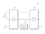
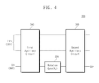
- FIG. 4 is a block diagram of a quantum circuit according to an embodiment of the inventive concept.
- a quantum circuit 300 includes a rotation gate 320 , a first auxiliary circuit 340 , and a second auxiliary circuit 360 .
- the quantum circuit 300 is a circuit for implementing a controlled-rotation gate such as the quantum circuit 100 or 200 shown in FIG. 1 or FIG. 2 .
- the quantum circuit 300 shifts the phase of the target qubit by ⁇ /2 n ⁇ 1 based on the state of the control qubit.
- the rotation gate 320 is a single-qubit-based gate.
- the rotation gate 320 may shift the phase of the inputted target qubit by ⁇ /2 n ⁇ 1 .
- the rotation gate 320 may be defined as the Rn gate in Equation 1.
- a logic qubit 301 with a 2-qubit state and an ancillary qubit 302 are inputted to the quantum circuit 200 .
- the logic qubit 301 includes a control qubit and a target qubit.
- the ancillary qubit 302 may have a
- This qubit state may be expressed mathematically as a tensor product (
- ⁇ > a 00
- the first auxiliary circuit 340 converts the first qubit state according to entanglement of logic qubit 301 and ancillary qubit 302 into a second qubit state.
- the second qubit state is determined according to the structure of the first auxiliary circuit 340 , and this structure will be described later with reference to FIG. 5 and FIG. 6 .
- the first auxiliary circuit 340 includes a plurality of basic gates. As described above, the basic gate may be an H-gate, a T-gate, or a CNOT gate.
- the first auxiliary circuit 340 may have fewer basic gates than the controlled-swap gate 240 of FIG. 3 .
- the first auxiliary circuit 340 may be configured to operate with fewer operations or fewer T-gate operations than the controlled-swap gate 240 of FIG. 3 .
- the operation time and resources of the quantum computing may be reduced.
- the rotation gate 320 shifts the phase for some basis states by ⁇ /2 n ⁇ 1 in the second qubit state converted by the first auxiliary circuit 340 .
- the second qubit state may be converted to the third qubit state.
- the rotation gate 320 for converting from the second qubit state to the third qubit state may be expressed by the unit matrix I and the tensor product of the Rn gate according to Equation 1, such as (I ⁇ I ⁇ Rn).
- the second auxiliary circuit 360 converts the third qubit state converted by the rotation gate 320 into the fourth qubit state.
- the fourth qubit state may be equal to the state according to the entanglement of the control qubit, the target qubit phase shifted by ⁇ /2 n ⁇ 1 , and the ancillary qubit of
- the second auxiliary circuit 360 includes a plurality of basic gates.
- the second auxiliary circuit 360 may have fewer basic gates than the controlled-swap gate 240 of FIG. 3 .
- the second auxiliary circuit 360 may be configured to operate with fewer operations or fewer T-gate operations than the controlled-swap gate 240 of FIG. 3 .
- the operation time and resources of the quantum computing may be reduced.
- the structure of the second auxiliary circuit 360 may be the same as that of the first auxiliary circuit 340 .
- the second auxiliary circuit 360 may be Hermitian with the first auxiliary circuit 340 .
- the structure of the second auxiliary circuit 360 will be described later in detail with reference to FIGS. 5 and 6 .
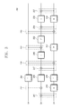
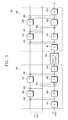
- FIG. 5 is a circuit diagram embodying an embodiment of the quantum circuit of FIG. 4
- a quantum circuit 400 includes a rotation gate 420 , a first auxiliary circuit 440 , and a second auxiliary circuit 460 .
- the rotation gate 420 corresponds to the rotation gate 320 of FIG. 4
- the first auxiliary circuit 440 corresponds to the first auxiliary circuit 340 of FIG. 4
- the second auxiliary circuit 460 corresponds to the second auxiliary circuit 360 of FIG. 4 .
- the logic qubit 401 including the control qubit and the target qubit, and the ancillary qubit 402 are inputted to the quantum circuit 400 .
- the logic qubit 401 corresponds to the logic qubit 301 of FIG. 4 and the ancillary qubit 402 corresponds to the ancillary qubit 302 of FIG. 4 .
- the first auxiliary circuit 440 includes a first H-gate 441 , a first CNOT gate 442 , a first T-gate 443 , a second T-gate (T ⁇ -gate) 444 , a second CNOT gate 445 , a third CNOT gate 446 , a third T-gate (T ⁇ -gate) 447 , a fourth T-gate 448 , a fourth CNOT gate 449 , and a second H-gate 450 .
- the H-gate, T-gate, and CNOT gate included in the first auxiliary circuit 440 may be defined as described in Equations 2 and 3.
- the first auxiliary circuit 440 includes a total of 10 basic gates.
- a controlled-rotation gate may be implemented using fewer basic gates than the controlled-swap gate 240 including the 17 basic gates of FIG. 3 . Further, since the quantum circuit 400 includes a smaller number of rotation gates than the quantum circuit 100 ′ of FIG. 1 , controlled-rotation gates may be implemented with fewer basic gates than in FIG. 1 .
- the first H-gate 441 performs Hadamard transform on the ancillary qubit 402 .
- the first CNOT gate 442 performs a CNOT calculation on the control qubit based on the ancillary qubit converted by the first H-gate 441 .
- the first T-gate 443 shifts the phase of the control qubit converted by the first CNOT gate 442 by ⁇ /8.
- the second T-gate 444 shifts the phase of the ancillary qubit converted by the first H-gate 441 by ⁇ /8.
- the second CNOT gate 445 performs a CNOT calculation on the control qubit converted by the first T-gate 443 based on the target qubit.
- the third CNOT gate 446 performs a CNOT calculation on the ancillary qubit converted by the second T-gate 444 based on the target qubit.
- the third T-gate 447 shifts the phase of the control qubit converted by the first CNOT gate 445 by ⁇ /8.
- the fourth T-gate 448 shifts the phase of the ancillary qubit converted by the third CNOT gate 446 by ⁇ /8.
- the fourth CNOT gate 449 performs a CNOT calculation on the control qubit converted by the third T-gate 447 based on the ancillary qubit converted by the fourth T-gate 448 .
- the second H-gate 450 performs Hadamard transform on the ancillary qubit converted by the fourth T-gate 448 .
- the first auxiliary circuit 440 operates in a total of 8 operations.
- the first auxiliary circuit 440 may operate with fewer operations than the controlled-swap gate 240 operating with a total of 10 operations of FIG. 3 .
- the first auxiliary circuit 440 operates with less than two T-gate operations than the controlled-swap gate 240 of FIG. 3 . That is, the operation time of the quantum circuit 400 and the resources for quantum computing may be reduced.
- an operation of the first auxiliary circuit 440 proceeds from right to left.
- (I ⁇ I ⁇ H) calculation is performed for the 3-qubit state (
- C 31 ⁇ calculation is performed by the first CNOT gate 442 .
- (T ⁇ I ⁇ T ⁇ ) calculation is performed by the first and second T-gates 443 and 444 .
- C 21 ⁇ calculation is performed by the second CNOT gate 445 .
- C 23 ⁇ calculation is performed by the third CNOT gate 446 .
- Equation 4 The calculation result of Equation 4 may be expressed as Equation 5.
- U
- the first auxiliary circuit 440 may not convert the values of
- the first auxiliary circuit 440 may shift the phase for the
- the first auxiliary circuit 440 may shift the phase for the
- the first auxiliary circuit 440 may shift the phase for the
- the second auxiliary circuit 460 includes a third H-gate 461 , a fifth CNOT gate 462 , a fifth T-gate 463 , a sixth T-gate (T ⁇ -gate) 464 , a sixth CNOT gate 465 , a seventh CNOT gate 466 , a seventh T-gate (T ⁇ -gate) 467 , an eighth T-gate 468 , an eighth CNOT gate 469 , and a fourth H-gate 450 . Since the arrangement structure of the basic gates included in the second auxiliary circuit 460 is the same as the arrangement structure of the basic gates included in the first auxiliary circuit 440 , a detailed description thereof will be omitted.
- the rotation gate 420 , the first auxiliary circuit 440 , and the second auxiliary circuit 460 may be implemented to perform the same operation as the controlled-rotation gate, as shown in Equation 6.
- 0>) U ( I ⁇ I ⁇ Rn ) U ( a 00
- 110>) U ( I ⁇ I ⁇ Rn )( a 00
- 111>) U ( a 00
- 111>) a 00
- 100> e i ⁇ /2 n ⁇ 1 a 11
- 110> (Controlled ⁇ Rn ⁇ I )(
- the first auxiliary circuit 440 , the single-qubit-based rotation gate 420 , and the second auxiliary circuit 460 are operated from the right side to the left side.
- the first auxiliary circuit 440 the value of the
- the rotation gate 420 the value of the
- the second auxiliary circuit 460 the value of the
- the quantum circuit 400 has the same effect as the operation of the controlled-rotation gate.
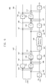
- FIG. 6 is a circuit diagram embodying an embodiment of the quantum circuit of FIG. 4
- a quantum circuit 500 includes a rotation gate 520 , a first auxiliary circuit 540 , and a second auxiliary circuit 560 .
- the rotation gate 520 corresponds to the rotation gate 320 of FIG. 4
- the first auxiliary circuit 540 corresponds to the first auxiliary circuit 340 of FIG. 4
- the second auxiliary circuit 560 corresponds to the second auxiliary circuit 360 of FIG. 4 .
- the logic qubit 501 including the control qubit and the target qubit, and the ancillary qubit 502 are inputted to the quantum circuit 500 .
- the logic qubit 501 corresponds to the logic qubit 301 of FIG. 4 and the ancillary qubit 502 corresponds to the ancillary qubit 302 of FIG. 4 .
- the first auxiliary circuit 540 includes a first H-gate 541 , a first CNOT gate 542 , a second CNOT gate 543 , a first T-gate 544 , a second T-gate (T ⁇ -gate) 545 , a third CNOT gate 546 , a fourth CNOT gate 547 , a third T-gate (T ⁇ -gate) 548 , a fourth T-gate 549 , a fifth CNOT gate 550 , a sixth CNOT gate 551 , and a second H-gate 552 .
- the H-gate, T-gate, and CNOT gate included in the first auxiliary circuit 540 may be defined as described in Equations 2 and 3.
- the first auxiliary circuit 540 includes a total of 12 basic gates. Thus, a controlled-rotation gate may be implemented using fewer basic gates than the swap gate 240 including the 17 basic gates of FIG. 3 .
- the first H-gate 541 performs Hadamard transform on the ancillary qubit 502 .
- the first CNOT gate 542 performs a CNOT calculation on the target qubit based on the ancillary qubit converted by the first H-gate 541 .
- the second CNOT gate 543 performs a CNOT calculation on the control qubit based on the target qubit converted by the first CNOT gate 542 .
- the first T-gate 544 shifts the phase of the control qubit converted by the second CNOT gate 543 by ⁇ /8.
- the second T-gate 545 shifts the phase of the target qubit converted by the first CNOT gate 542 by ⁇ /8.
- the third CNOT gate 546 performs a CNOT calculation on the target qubit converted by the second T-gate 545 based on the ancillary qubit converted by the first H-gate 541 .
- the fourth CNOT gate 547 performs a CNOT calculation on the target qubit converted by the third CNOT gate 546 based on the control qubit converted by the first T-gate 544 .
- the third T-gate 548 shifts the phase of the target qubit converted by the fourth CNOT gate 547 by ⁇ /8.
- the fourth T-gate 549 shifts the phase of the ancillary qubit converted by the first H-gate 541 by ⁇ /8.
- the fifth CNOT gate 550 performs a CNOT calculation on the control qubit converted by the first T-gate 544 based on the target qubit converted by the third T-gate 548 .
- the sixth CNOT gate 551 performs a CNOT calculation on the target qubit converted by the third T-gate 548 based on the ancillary qubit converted by the fourth T-gate 549 .
- the second H-gate 552 performs Hadamard transform on the ancillary qubit converted by the fourth T-gate 549 .
- the first auxiliary circuit 540 has more basic gates than the first auxiliary circuit 440 of FIG. 5 and operates with more operations. However, the first auxiliary circuit 540 of FIG. 6 considers the physically implemented distance between the qubits.
- the CNOT gates included in the first auxiliary circuit 540 are implemented to perform CNOT calculations on adjacent qubits. CNOT gates included in the first auxiliary circuit 540 are implemented not to perform CNOT calculations on non-contiguous qubits (e.g., ancillary qubits and control qubits).
- the first auxiliary circuit 540 operates in a total of 10 operations and operates with a total of two T-gate operations. Since the first auxiliary circuit 540 operates with fewer T-gate operations than the controlled-swap gate 240 of FIG. 3 , the operation time of the quantum circuit 500 and the resources for quantum computing may be reduced.
- an operation of the first auxiliary circuit 540 proceeds from right to left.
- (I ⁇ I ⁇ H) calculation is performed for the 3-qubit state (
- C 32 ⁇ calculation is performed by the first CNOT gate 542 .
- C 21 ⁇ calculation is performed by the second CNOT gate 543 .
- (T ⁇ T ⁇ ⁇ I) calculation is performed by the first and second T-gates 544 and 545 .
- C 31 ⁇ calculation is performed by the third CNOT gate 546 .
- Equation 7 may be expressed as Equation 8.
- the first auxiliary circuit 540 may not convert the values of the
- the first auxiliary circuit 540 may exchange the values of the
- the first auxiliary circuit 540 may shift the phase for the
- the first auxiliary circuit 440 may shift the phase for the
- the second auxiliary circuit 560 may be Hermitian with the first auxiliary circuit 540 .
- the second auxiliary circuit 560 includes a third H-gate 561 , a seventh CNOT gate 562 , an eighth CNOT gate 563 , a fifth T-gate 564 , a sixth T-gate (T ⁇ -gate) 565 , a ninth CNOT gate 566 , a tenth CNOT gate 567 , a seventh T-gate (T ⁇ -gate) 568 , an eighth T-gate 569 , an eleventh CNOT gate 570 , a twelfth CNOT gate 571 , and a fourth H-gate 572 .
- the number of basic gates included in the second auxiliary circuit 560 is equal to the number of basic gates included in the first auxiliary circuit 540 . Since the arrangement of the third H-gate 561 , the seventh CNOT gate 562 , the eighth CNOT gate 563 , the eleventh CNOT gate 570 , the twelfth CNOT gate 571 , and the fourth H-gate 572 is equal to the arrangement of the first H-gate 541 , the first CNOT gate 542 , the second CNOT gate 543 , the fifth CNOT gate 550 , the sixth CNOT gate 551 , and the second H-gate 552 of the first auxiliary circuit 540 , a detailed description thereof is omitted.
- the second auxiliary circuit 560 has a difference in the arrangement of a fifth T-gate 564 , a sixth T-gate 565 , a ninth CNOT gate 566 , a tenth CNOT gate 567 , a seventh T-gate 568 , and an eighth T-gate 569 .
- the fifth T-gate 564 shifts the phase of the target qubit converted by the seventh CNOT gate 562 by ⁇ /8.
- the sixth T-gate 565 shifts the phase of the ancillary qubit converted by the third H-gate 561 by ⁇ /8.
- the ninth CNOT gate 566 performs a CNOT calculation on the target qubit converted by the fifth T-gate 564 based on the control qubit converted by the eighth CNOT gate 563 .
- the tenth CNOT gate 567 performs a CNOT calculation on the target qubit converted by the ninth CNOT gate 566 based on the ancillary qubit converted by the sixth T-gate 565 .
- the seventh T-gate 568 shifts the phase of the control qubit converted by the eighth CNOT gate 563 by ⁇ /8.
- the eighth T-gate 569 shifts the phase of the target qubit converted by the tenth CNOT gate 567 by ⁇ /8.
- the rotation gate 520 , the first auxiliary circuit 540 , and the second auxiliary circuit 560 may be implemented to perform the same operation as the controlled-rotation gate, as shown in Equation 9.
- 0>) U ⁇ ( I ⁇ I ⁇ Rn ) U ( a 00
- 110>) U ⁇ ( I ⁇ I ⁇ Rn )( a 00
- 111>) U ⁇ ( a 00
- 111>) a 00
- 110> (Controlled ⁇ Rn ⁇ I
- the first auxiliary circuit 540 , the single-qubit-based rotation gate 520 , and the second auxiliary circuit 560 are operated from the right side to the left side.
- the first auxiliary circuit 540 the value of the
- the first auxiliary circuit 540 the value of the
- the rotation gate 520 the value of the
- the quantum circuit 500 has the same effect as the operation of the controlled-rotation gate.
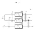
- FIG. 7 is a circuit diagram of a quantum circuit according to an embodiment of the inventive concept.
- a quantum circuit 600 includes a first CNOT gate 610 , a second CNOT gate 620 , a first rotation gate 630 , a second rotation gate 640 , a third rotation gate 650 , a third CNOT gate 660 , and a fourth CNOT gate 670 .
- the quantum circuit 600 is a circuit for implementing a controlled-rotation gate such as the quantum circuit 100 or 200 shown in FIG. 1 or FIG. 2 .
- the quantum circuit 600 shifts the phase of the target qubit by ⁇ /2 n ⁇ 1 based on the state of the control qubit.
- a logic qubit 601 and an ancillary qubit 602 are inputted to the quantum circuit 600 .
- the logic qubit 601 includes a control qubit and a target qubit.
- the ancillary qubit 602 may have a
- the first CNOT gate 610 performs a CNOT calculation on the ancillary qubit, based on the target qubit.
- the second CNOT gate 620 performs a CNOT calculation on the target qubit, based on the control qubit.
- the first rotation gate 630 shifts the phase of the control qubit by ⁇ /2 n .
- the second rotation gate 640 shifts the phase of the target qubit converted by the second CNOT gate 620 by ⁇ /2 n .
- the third rotation gate 650 shifts the phase of the ancillary qubit converted by the first CNOT gate 610 by ⁇ /2 n .
- the third CNOT gate 660 may perform a CNOT calculation on the target qubit converted by the second rotation gate 640 based on the control qubit converted by the first rotation gate 630 .
- the fourth CNOT gate 670 performs a CNOT calculation on the ancillary qubit converted by the third rotation gate 660 based on the target qubit converted by the third CNOT gate 650 .
- the quantum circuit 600 operates in a total of five operations. That is, the quantum circuit 600 of FIG. 7 may operate with minimum operations. Although the quantum circuit 100 ′ decomposed into single-qubit-based rotation gates in FIG. 1 operates in four operations, since the operation time of the rotation gate is considerably larger than that of other basic gates, actually, the operation time of the quantum circuit 600 of FIG. 7 is shorter than that of the quantum circuit 100 ′ of FIG. 1 . The reason is that the first to third rotation gates 630 , 640 , and 650 operate in parallel in one operation in the quantum circuit 600 . The quantum circuit 600 may be implemented to perform the same operation as the controlled-rotation gate, as shown in Equation 10.
- a first CNOT gate 610 , a second CNOT gate 620 , a first rotation gate 630 , a second rotation gate 640 , a third rotation gate 650 , a third CNOT gate 660 , and a fourth CNOT gate 670 operate from right to left.
- C 23 ⁇ calculation is performed by the first CNOT gate 610 .
- C 12 ⁇ calculation is performed by the second CNOT gate 620 .
- (R n+1 ⁇ R ⁇ n+1 ⁇ R n+1 ⁇ R n+1 ) calculation is performed by the first to third rogation gates 630 , 640 , and 650 .
- C 12 ⁇ calculation is performed by the third CNOT gate 660 .
- C 23 ⁇ calculation is performed by the fourth CNOT gate 670 .
- 010> basis state is determined as the value of the
- 100> basis state is determined as the value of the
- 110> basis state is determined as the value of the
- the first to third rotation gates 630 , 640 and 650 the value of the
- 011> basis state is determined as the value of the
- 110> basis state is determined as the value of the
- 101> basis state is determined as the value of the
- a quantum computer in which a quantum circuit is implemented may be composed of a plurality of components that perform various functions.
- a quantum computer in which the above-described quantum circuit is implemented may include a CPU for processing quantum information, a memory for storing quantum information, and a bus for transferring information between the CPU and the memory.
- the CPU may function as a central processing unit of the quantum computer.
- the CPU may operate using the calculation space of the memory, and the quantum circuit may perform the operation of the controlled-rotation gate using the control qubit, the target qubit, and the ancillary qubit according to the control of the CPU.
- the quantum circuit may generate the control qubit, the target qubit, and the ancillary qubit under the control of the CPU and shift the phase of the target qubit by n/2 n ⁇ 1 based on the state of the control qubit.
- a quantum circuit that shifts the phase of the target qubit based on the control qubit uses an ancillary qubit and reduces the number of basic gates, thereby reducing the resource and operation time of the quantum computing.
Abstract
Description
U=(I⊗I⊗H)C 31(T † ⊗I⊗T)C 23 C 21(T⊗I⊗T †)C 31(I⊗I⊗H) [Equation 4]
U=|000><000|+|001><001|+|010><010|−|011><011|
+|100><100|+|101><101|+i|110><111|−i|111><110| [Equation 5]
U(I⊗I⊗Rn)U(|Ψ>⊗|0>)
=U(I⊗I⊗Rn)U(a 00|000>+a 01|010>+a 10|100>+a 11|110>)
=U(I⊗I⊗Rn)(a 00|000>+a 01|010>+a 10|100>−ia 11|111>)
=U(a 00|000>+a 01|010>+a 10|100>+e iπ/2
=a 00|000+a 01|010>+a 10|100>=e iπ/2
=(Controlled−Rn⊗I)(|Ψ>⊗|0>) [Equation 6]
U=(I⊗I⊗H)C 32 C 21(I⊗T † ⊗T)C 12 C 31(T⊗T † ⊗I)C 21 C 32(I⊗I⊗H) [Equation 7]
U=|000><000|+|001><001|+|010><100|+|011><101|
+|100><010|+|101><011|−i|110><111|−i|111><110| [Equation 8]
U †(I⊗I⊗Rn)U(|Ψ>⊗|0>)
=U †(I⊗I⊗Rn)U(a 00|000>+a 01|010>+a 10|100>+a 11|110>)
=U †(I⊗I⊗Rn)(a 00|000>+a 01|100>+a 10|010>−ia 11|111>)
=U †(a 00|000>+a 01|100>+a 10|010>−ie iπ/2
=a 00|000>+a 01|010>+a 10|100>+e iπ/2
=(Controlled−Rn⊗I)(|Ψ>⊗|0>) [Equation 9]
C 23 C 12(R n+1 ⊗R † n+1 ⊗R n+1)C 12 C 23(|Ψ⊗|0>)
=C 23 C 12(R n+1 ⊗R † n+1 ⊗R n+1)(a 00|000>+a 01|011>+a 10|110>+a 11|101>)
=C 23 C 12(a 00|000>+a 01|011>+a 10|110>+e iπ/2
=a 00|000>+a 01|010>+a 10|100>+e iπ/2
=(Controlled−Rn⊗I)(|Ψ>⊗|0>) [Equation 10]
Claims (16)
Applications Claiming Priority (4)
| Application Number | Priority Date | Filing Date | Title |
|---|---|---|---|
| KR10-2017-0088649 | 2017-07-12 | ||
| KR20170088649 | 2017-07-12 | ||
| KR1020180072376A KR102338755B1 (en) | 2017-07-12 | 2018-06-22 | Quantum circuit for phase shift of target qubit based on control qubit |
| KR10-2018-0072376 | 2018-06-22 |
Publications (2)
| Publication Number | Publication Date |
|---|---|
| US10171088B1 true US10171088B1 (en) | 2019-01-01 |
| US20190020345A1 US20190020345A1 (en) | 2019-01-17 |
Family
ID=64739734
Family Applications (1)
| Application Number | Title | Priority Date | Filing Date |
|---|---|---|---|
| US16/034,073 Active US10171088B1 (en) | 2017-07-12 | 2018-07-12 | Quantum circuit for shifting phase of target qubit based on control qubit |
Country Status (1)
| Country | Link |
|---|---|
| US (1) | US10171088B1 (en) |
Cited By (6)
| Publication number | Priority date | Publication date | Assignee | Title |
|---|---|---|---|---|
| US10496933B1 (en) * | 2018-12-19 | 2019-12-03 | Microsoft Technology Licensing, Llc | Robust Majorana magic gates via measurements |
| US11049038B2 (en) * | 2019-03-29 | 2021-06-29 | Alibaba Group Holding Limited | Methods and systems for optimizing quantum circuits |
| WO2021165108A1 (en) * | 2020-02-19 | 2021-08-26 | International Business Machines Corporation | Target qubit decoupling in an echoed cross-resonance gate |
| US11580000B2 (en) * | 2017-07-23 | 2023-02-14 | Keysight Technologies Canada Inc. | Systems and methods for local randomized benchmarking |
| US11762733B2 (en) | 2020-11-23 | 2023-09-19 | Electronics And Telecommunications Research Institute | Quantum computing system and operation method thereof |
| JP7422768B2 (en) | 2019-02-08 | 2024-01-26 | インターナショナル・ビジネス・マシーンズ・コーポレーション | quantum circuit layout |
Citations (5)
| Publication number | Priority date | Publication date | Assignee | Title |
|---|---|---|---|---|
| US20040264898A1 (en) * | 2001-08-28 | 2004-12-30 | Munro William John | Quantum information processing method and apparatus |
| US20060056631A1 (en) * | 2004-09-13 | 2006-03-16 | Beausoleil Raymond G | Tests of quantum information |
| US7496203B2 (en) | 2004-04-13 | 2009-02-24 | Electronics And Telecommunications Research Institute | Quantum-key distribution method between a plurality of users or groups |
| US20100150349A1 (en) | 2008-12-12 | 2010-06-17 | Electronics And Telecommunications Research Institute | Method and system for performing quantum bit commitment protocol |
| US7791780B2 (en) * | 2004-07-26 | 2010-09-07 | Hewlett-Packard Development Company, L.P. | Quantum coherent systems and operations |
-
2018
- 2018-07-12 US US16/034,073 patent/US10171088B1/en active Active
Patent Citations (5)
| Publication number | Priority date | Publication date | Assignee | Title |
|---|---|---|---|---|
| US20040264898A1 (en) * | 2001-08-28 | 2004-12-30 | Munro William John | Quantum information processing method and apparatus |
| US7496203B2 (en) | 2004-04-13 | 2009-02-24 | Electronics And Telecommunications Research Institute | Quantum-key distribution method between a plurality of users or groups |
| US7791780B2 (en) * | 2004-07-26 | 2010-09-07 | Hewlett-Packard Development Company, L.P. | Quantum coherent systems and operations |
| US20060056631A1 (en) * | 2004-09-13 | 2006-03-16 | Beausoleil Raymond G | Tests of quantum information |
| US20100150349A1 (en) | 2008-12-12 | 2010-06-17 | Electronics And Telecommunications Research Institute | Method and system for performing quantum bit commitment protocol |
Non-Patent Citations (1)
| Title |
|---|
| Vadym Kliuchnikov et al., "Fast and efficient exact synthesis of single qubit unitaries generated by Clifford and T gates", Quantum Information and Computation, Mar. 1, 2013, vol. 13, No. 7-8, pp. 607-630. |
Cited By (7)
| Publication number | Priority date | Publication date | Assignee | Title |
|---|---|---|---|---|
| US11580000B2 (en) * | 2017-07-23 | 2023-02-14 | Keysight Technologies Canada Inc. | Systems and methods for local randomized benchmarking |
| US10496933B1 (en) * | 2018-12-19 | 2019-12-03 | Microsoft Technology Licensing, Llc | Robust Majorana magic gates via measurements |
| JP7422768B2 (en) | 2019-02-08 | 2024-01-26 | インターナショナル・ビジネス・マシーンズ・コーポレーション | quantum circuit layout |
| US11049038B2 (en) * | 2019-03-29 | 2021-06-29 | Alibaba Group Holding Limited | Methods and systems for optimizing quantum circuits |
| WO2021165108A1 (en) * | 2020-02-19 | 2021-08-26 | International Business Machines Corporation | Target qubit decoupling in an echoed cross-resonance gate |
| US11695483B2 (en) | 2020-02-19 | 2023-07-04 | International Business Machines Corporation | Target qubit decoupling in an echoed cross-resonance gate |
| US11762733B2 (en) | 2020-11-23 | 2023-09-19 | Electronics And Telecommunications Research Institute | Quantum computing system and operation method thereof |
Also Published As
| Publication number | Publication date |
|---|---|
| US20190020345A1 (en) | 2019-01-17 |
Similar Documents
| Publication | Publication Date | Title |
|---|---|---|
| US10171088B1 (en) | Quantum circuit for shifting phase of target qubit based on control qubit | |
| Amy et al. | On the controlled-NOT complexity of controlled-NOT–phase circuits | |
| Pavlidis et al. | Fast quantum modular exponentiation architecture for shor's factorization algorithm | |
| Maslov | Advantages of using relative-phase Toffoli gates with an application to multiple control Toffoli optimization | |
| Chakrabarti et al. | Linear nearest neighbor synthesis of reversible circuits by graph partitioning | |
| Jayashree et al. | Ancilla-input and garbage-output optimized design of a reversible quantum integer multiplier | |
| Hebenstreit et al. | All pure fermionic non-gaussian states are magic states for matchgate computations | |
| WO2014151571A2 (en) | Method and system for decomposing single-qubit quantum circuits into a discrete basis | |
| CN111582491A (en) | Construction method and device of quantum line | |
| Arrighi et al. | The physical Church-Turing thesis and the principles of quantum theory | |
| Pham et al. | A 2D nearest-neighbor quantum architecture for factoring in polylogarithmic depth. | |
| Niemann et al. | Improved synthesis of Clifford+ T quantum functionality | |
| CN115668232A (en) | Implementation of N-qubit quantum gates | |
| CN115801244A (en) | Post-quantum cryptography algorithm implementation method and system for resource-constrained processor | |
| Litinski et al. | Active volume: An architecture for efficient fault-tolerant quantum computers with limited non-local connections | |
| Seyedi et al. | A new design for 4-bit RCA using quantum cellular automata technology | |
| Abdessaied et al. | Complexity of reversible circuits and their quantum implementations | |
| Zakablukov | Application of permutation group theory in reversible logic synthesis | |
| Szyprowski et al. | A study of optimal 4-bit reversible circuit synthesis from mixed-polarity Toffoli gates | |
| CN110417545B (en) | Finite field discrete logarithm quantum solution line optimization construction method | |
| Pham et al. | A 2D nearest-neighbor quantum architecture for factoring in polylogarithmic depth | |
| Devulapalli et al. | Quantum routing with teleportation | |
| JP4332167B2 (en) | Quantum circuit for performing approximate quantum Fourier transform, approximate quantum Fourier transform calculation method and apparatus | |
| KR102338755B1 (en) | Quantum circuit for phase shift of target qubit based on control qubit | |
| Kotiyal et al. | Design methodologies for reversible logic based barrel shifters |
Legal Events
| Date | Code | Title | Description |
|---|---|---|---|
| FEPP | Fee payment procedure |
Free format text: ENTITY STATUS SET TO UNDISCOUNTED (ORIGINAL EVENT CODE: BIG.); ENTITY STATUS OF PATENT OWNER: SMALL ENTITY |
|
| AS | Assignment |
Owner name: ELECTRONICS AND TELECOMMUNICATIONS RESEARCH INSTIT Free format text: ASSIGNMENT OF ASSIGNORS INTEREST;ASSIGNORS:KIM, TAEWAN;CHOI, BYUNG-SOO;REEL/FRAME:046348/0215 Effective date: 20180629 |
|
| FEPP | Fee payment procedure |
Free format text: ENTITY STATUS SET TO SMALL (ORIGINAL EVENT CODE: SMAL); ENTITY STATUS OF PATENT OWNER: SMALL ENTITY |
|
| STCF | Information on status: patent grant |
Free format text: PATENTED CASE |
|
| MAFP | Maintenance fee payment |
Free format text: PAYMENT OF MAINTENANCE FEE, 4TH YR, SMALL ENTITY (ORIGINAL EVENT CODE: M2551); ENTITY STATUS OF PATENT OWNER: SMALL ENTITY Year of fee payment: 4 |