US10170722B2 - Organic light-emitting device having low work function metal halide compound in hole injection layer - Google Patents
Organic light-emitting device having low work function metal halide compound in hole injection layer Download PDFInfo
- Publication number
- US10170722B2 US10170722B2 US14/633,365 US201514633365A US10170722B2 US 10170722 B2 US10170722 B2 US 10170722B2 US 201514633365 A US201514633365 A US 201514633365A US 10170722 B2 US10170722 B2 US 10170722B2
- Authority
- US
- United States
- Prior art keywords
- group
- layer
- electrode
- emitting device
- organic light
- Prior art date
- Legal status (The legal status is an assumption and is not a legal conclusion. Google has not performed a legal analysis and makes no representation as to the accuracy of the status listed.)
- Active, expires
Links
Images


Classifications
-
- H—ELECTRICITY
- H10—SEMICONDUCTOR DEVICES; ELECTRIC SOLID-STATE DEVICES NOT OTHERWISE PROVIDED FOR
- H10K—ORGANIC ELECTRIC SOLID-STATE DEVICES
- H10K50/00—Organic light-emitting devices
- H10K50/10—OLEDs or polymer light-emitting diodes [PLED]
- H10K50/14—Carrier transporting layers
- H10K50/15—Hole transporting layers
-
- H01L51/5088—
-
- H—ELECTRICITY
- H10—SEMICONDUCTOR DEVICES; ELECTRIC SOLID-STATE DEVICES NOT OTHERWISE PROVIDED FOR
- H10K—ORGANIC ELECTRIC SOLID-STATE DEVICES
- H10K50/00—Organic light-emitting devices
- H10K50/10—OLEDs or polymer light-emitting diodes [PLED]
- H10K50/14—Carrier transporting layers
- H10K50/15—Hole transporting layers
- H10K50/155—Hole transporting layers comprising dopants
-
- H—ELECTRICITY
- H10—SEMICONDUCTOR DEVICES; ELECTRIC SOLID-STATE DEVICES NOT OTHERWISE PROVIDED FOR
- H10K—ORGANIC ELECTRIC SOLID-STATE DEVICES
- H10K50/00—Organic light-emitting devices
- H10K50/10—OLEDs or polymer light-emitting diodes [PLED]
- H10K50/14—Carrier transporting layers
- H10K50/15—Hole transporting layers
- H10K50/156—Hole transporting layers comprising a multilayered structure
-
- H—ELECTRICITY
- H10—SEMICONDUCTOR DEVICES; ELECTRIC SOLID-STATE DEVICES NOT OTHERWISE PROVIDED FOR
- H10K—ORGANIC ELECTRIC SOLID-STATE DEVICES
- H10K50/00—Organic light-emitting devices
- H10K50/10—OLEDs or polymer light-emitting diodes [PLED]
- H10K50/17—Carrier injection layers
-
- H—ELECTRICITY
- H10—SEMICONDUCTOR DEVICES; ELECTRIC SOLID-STATE DEVICES NOT OTHERWISE PROVIDED FOR
- H10K—ORGANIC ELECTRIC SOLID-STATE DEVICES
- H10K50/00—Organic light-emitting devices
- H10K50/10—OLEDs or polymer light-emitting diodes [PLED]
- H10K50/17—Carrier injection layers
- H10K50/171—Electron injection layers
-
- H—ELECTRICITY
- H10—SEMICONDUCTOR DEVICES; ELECTRIC SOLID-STATE DEVICES NOT OTHERWISE PROVIDED FOR
- H10K—ORGANIC ELECTRIC SOLID-STATE DEVICES
- H10K50/00—Organic light-emitting devices
- H10K50/80—Constructional details
- H10K50/805—Electrodes
- H10K50/81—Anodes
- H10K50/816—Multilayers, e.g. transparent multilayers
-
- H—ELECTRICITY
- H10—SEMICONDUCTOR DEVICES; ELECTRIC SOLID-STATE DEVICES NOT OTHERWISE PROVIDED FOR
- H10K—ORGANIC ELECTRIC SOLID-STATE DEVICES
- H10K85/00—Organic materials used in the body or electrodes of devices covered by this subclass
- H10K85/30—Coordination compounds
- H10K85/341—Transition metal complexes, e.g. Ru(II)polypyridine complexes
- H10K85/342—Transition metal complexes, e.g. Ru(II)polypyridine complexes comprising iridium
-
- H—ELECTRICITY
- H10—SEMICONDUCTOR DEVICES; ELECTRIC SOLID-STATE DEVICES NOT OTHERWISE PROVIDED FOR
- H10K—ORGANIC ELECTRIC SOLID-STATE DEVICES
- H10K85/00—Organic materials used in the body or electrodes of devices covered by this subclass
- H10K85/60—Organic compounds having low molecular weight
- H10K85/615—Polycyclic condensed aromatic hydrocarbons, e.g. anthracene
-
- H—ELECTRICITY
- H10—SEMICONDUCTOR DEVICES; ELECTRIC SOLID-STATE DEVICES NOT OTHERWISE PROVIDED FOR
- H10K—ORGANIC ELECTRIC SOLID-STATE DEVICES
- H10K85/00—Organic materials used in the body or electrodes of devices covered by this subclass
- H10K85/60—Organic compounds having low molecular weight
- H10K85/631—Amine compounds having at least two aryl rest on at least one amine-nitrogen atom, e.g. triphenylamine
-
- H—ELECTRICITY
- H10—SEMICONDUCTOR DEVICES; ELECTRIC SOLID-STATE DEVICES NOT OTHERWISE PROVIDED FOR
- H10K—ORGANIC ELECTRIC SOLID-STATE DEVICES
- H10K85/00—Organic materials used in the body or electrodes of devices covered by this subclass
- H10K85/60—Organic compounds having low molecular weight
- H10K85/649—Aromatic compounds comprising a hetero atom
- H10K85/657—Polycyclic condensed heteroaromatic hydrocarbons
- H10K85/6572—Polycyclic condensed heteroaromatic hydrocarbons comprising only nitrogen in the heteroaromatic polycondensed ring system, e.g. phenanthroline or carbazole
-
- H01L2251/301—
-
- H01L51/0058—
-
- H01L51/006—
-
- H01L51/0067—
-
- H01L51/0072—
-
- H01L51/0085—
-
- H01L51/0087—
-
- H01L51/0088—
-
- H—ELECTRICITY
- H10—SEMICONDUCTOR DEVICES; ELECTRIC SOLID-STATE DEVICES NOT OTHERWISE PROVIDED FOR
- H10K—ORGANIC ELECTRIC SOLID-STATE DEVICES
- H10K2102/00—Constructional details relating to the organic devices covered by this subclass
-
- H—ELECTRICITY
- H10—SEMICONDUCTOR DEVICES; ELECTRIC SOLID-STATE DEVICES NOT OTHERWISE PROVIDED FOR
- H10K—ORGANIC ELECTRIC SOLID-STATE DEVICES
- H10K85/00—Organic materials used in the body or electrodes of devices covered by this subclass
- H10K85/30—Coordination compounds
- H10K85/341—Transition metal complexes, e.g. Ru(II)polypyridine complexes
- H10K85/346—Transition metal complexes, e.g. Ru(II)polypyridine complexes comprising platinum
-
- H—ELECTRICITY
- H10—SEMICONDUCTOR DEVICES; ELECTRIC SOLID-STATE DEVICES NOT OTHERWISE PROVIDED FOR
- H10K—ORGANIC ELECTRIC SOLID-STATE DEVICES
- H10K85/00—Organic materials used in the body or electrodes of devices covered by this subclass
- H10K85/30—Coordination compounds
- H10K85/341—Transition metal complexes, e.g. Ru(II)polypyridine complexes
- H10K85/348—Transition metal complexes, e.g. Ru(II)polypyridine complexes comprising osmium
-
- H—ELECTRICITY
- H10—SEMICONDUCTOR DEVICES; ELECTRIC SOLID-STATE DEVICES NOT OTHERWISE PROVIDED FOR
- H10K—ORGANIC ELECTRIC SOLID-STATE DEVICES
- H10K85/00—Organic materials used in the body or electrodes of devices covered by this subclass
- H10K85/60—Organic compounds having low molecular weight
- H10K85/615—Polycyclic condensed aromatic hydrocarbons, e.g. anthracene
- H10K85/626—Polycyclic condensed aromatic hydrocarbons, e.g. anthracene containing more than one polycyclic condensed aromatic rings, e.g. bis-anthracene
-
- H—ELECTRICITY
- H10—SEMICONDUCTOR DEVICES; ELECTRIC SOLID-STATE DEVICES NOT OTHERWISE PROVIDED FOR
- H10K—ORGANIC ELECTRIC SOLID-STATE DEVICES
- H10K85/00—Organic materials used in the body or electrodes of devices covered by this subclass
- H10K85/60—Organic compounds having low molecular weight
- H10K85/631—Amine compounds having at least two aryl rest on at least one amine-nitrogen atom, e.g. triphenylamine
- H10K85/633—Amine compounds having at least two aryl rest on at least one amine-nitrogen atom, e.g. triphenylamine comprising polycyclic condensed aromatic hydrocarbons as substituents on the nitrogen atom
-
- H—ELECTRICITY
- H10—SEMICONDUCTOR DEVICES; ELECTRIC SOLID-STATE DEVICES NOT OTHERWISE PROVIDED FOR
- H10K—ORGANIC ELECTRIC SOLID-STATE DEVICES
- H10K85/00—Organic materials used in the body or electrodes of devices covered by this subclass
- H10K85/60—Organic compounds having low molecular weight
- H10K85/649—Aromatic compounds comprising a hetero atom
- H10K85/654—Aromatic compounds comprising a hetero atom comprising only nitrogen as heteroatom
Definitions
- One or more exemplary embodiments relate to an organic light-emitting device.
- Organic light-emitting devices are self-emission devices that may have wide viewing angles, high contrast ratios, short response times, and excellent brightness, driving voltage, and response speed characteristics, and may produce full-color images.
- Embodiments may be realized by providing an organic light-emitting device, including a first electrode; a second electrode facing the first electrode; and an organic layer between the first electrode and the second electrode and including an emission layer, the organic layer including a low work function metal compound.
- the low work function metal compound may have a work function in a range of more than 0 eV to about 3 eV.
- the low work function metal compound may include a halide of an alkali metal.
- the low work function metal compound may include a halide of an alkaline earth metal.
- the low work function metal compound may include a halide of a lanthanide metal.
- the low work function metal compound may include a halide of Li, Na, K, Rb, Cs, Be, Mg, Ca, Sr, Ba, Yb, or Sm.
- the low work function metal compound may include LiF, NaF, KF, RbF, CsF, BeF 2 , MgF 2 , CaF 2 , SrF 2 , BaF 2 , YbF, YbF 2 , YbF 3 , or SmF 3 .
- the low work function metal compound may include LiCl, NaCl, KCl, RbCl, CsCl, BeCl 2 , MgCl 2 , CaCl 2 , SrCl 2 , BaCl 2 , YbCl, YbCl 2 , YbCl 3 , or SmCl 3 .
- the low work function metal compound may include LiBr, NaBr, KBr, RbBr, CsBr, BeBr 2 , MgBr 2 , CaBr 2 , SrBr 2 , BaBr 2 , YbBr, YbBr 2 , YbBr 3 , or SmBr 3 .
- the low work function metal compound may include LiI, NaI, KI, RbI, CsI, BeI 2 , MgI 2 , CaI 2 , SrI 2 , BaI 2 , YbI, YbI 2 , YbI 3 , or SmI 3 .
- the first electrode may be an anode
- the second electrode may be a cathode
- the organic layer may include a layer including the low work function metal compound, a hole transport region between the first electrode and the emission layer, and including one or more of a hole injection layer, a hole transport layer, or an electron blocking layer, and an electron transport region between the emission layer and the second electrode, and including one or more of a hole blocking layer, an electron transport layer, or an electron injection layer.
- the layer including the low work function metal compound may be in the hole transport region.
- the layer including the low work function metal compound may consist of a low work function metal compound.
- the thickness of the layer including the low work function metal compound may be in a range of about 1 ⁇ to about 30 ⁇ .
- the layer including the low work function metal compound may consist of a low work function metal compound and a hole injection material.
- the thickness of the layer including the low work function metal compound may be in a range of about 1 ⁇ to about 100 ⁇ .
- the layer including the low work function metal compound may contact an anode.
- the layer including the low work function metal compound may consist of a low work function metal compound.
- the layer including the low work function metal compound may consist of a low work function metal compound and a hole injection material.
- Embodiments may be realized by providing a flat display apparatus, including the presently disclosed organic light-emitting device.
- the first electrode of the organic light-emitting device may be electrically connected to a source or drain electrode of a thin film transistor.
- FIG. 1 illustrates a schematic view of an organic light-emitting device according to an embodiment
- FIG. 2 illustrates a schematic cross-sectional view of an organic light-emitting device according to an embodiment
- FIG. 3 illustrates a schematic cross-sectional view of an organic light-emitting device according to an embodiment
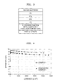
- FIG. 4 illustrates a graph of an efficiency of each of the devices of Example 1 and Comparative Example 1.
- the organic layer includes a layer including a low work function metal compound.
- a hole injection layer including CuI having a high work function may be used to provide a device that may lower an energy barrier of an anode and the hole injection layer.
- a hole injection barrier may be lowered when an organic light-emitting device includes a layer including a low work function metal compound.
- the low work function metal compound may rather increase an energy barrier.
- a metal compound used herein may have a strong binding force.
- the low work function metal compound may have a work function in a range of more than 0 eV to about 3 eV.
- the low work function metal compound may include a halide of an alkali metal, a halide of an alkaline earth metal, or a halide of a lanthanide metal.
- the low work function metal compound may include a halide of Li, Na, K, Rb, Cs, Be, Mg, Ca, Sr, Ba, Yb, or Sm.
- the low work function metal compound may include LiCl, NaCl, KCl, RbCl, CsCl, BeCl 2 , MgCl 2 , CaCl 2 , SrCl 2 , BaCl 2 , YbCl, YbCl 2 , YbCl 3 , SmCl 3 , LiBr, NaBr, KBr, RbBr, CsBr, BeBr 2 , MgBr 2 , CaBr 2 , SrBr 2 , BaBr 2 , YbBr, YbBr 2 , YbBr 3 , SmBr 3 , LiI, NaI, KI, RbI, CsI, BeI 2 , MgI 2 , CaI 2 , SrI 2 , BaI 2 , YbI, YbI 2 , YbI 3 , or SmI 3 .
- the low work function metal compound may include
- the first electrode may be an anode
- the second electrode may be a cathode
- the organic layer may include:
- a hole transport region disposed between the first electrode and the emission layer, and including at least one selected from a hole injection layer, a hole transport layer, and an electron blocking layer, and
- an electron transport region disposed between the emission layer and the second electrode, and including at least one selected from a hole blocking layer, an electron transport layer, and an electron injection layer.
- the layer including the low work function metal compound may be disposed in the hole transport region.
- the layer including the low work function metal compound may be formed of a low work function metal compound.
- the layer including the low work function metal compound may include only a low work function metal compound.
- the thickness of the layer that includes only a low work function metal compound may be in a range of about 1 ⁇ to about 30 ⁇ .
- the organic light-emitting device may have a maximum efficiency when the thickness of the layer is maintained within the aforementioned range.
- the layer including a low work function metal compound may be formed of a low work function metal compound and a hole injection material.
- the thickness of the layer formed of a low work function metal compound and a hole injection material may be in a range of about 1 ⁇ to about 100 ⁇ .
- the organic light-emitting device may have a maximum efficiency when the thickness of the layer is maintained within the aforementioned range.
- the volume percent ratio of low work function metal compound:hole injection material may be in a range of about 1:60 to about 60:1.
- the volume percent ratio may be in a range of about 1:50 to about 50:1.
- the organic light-emitting device may have a maximum efficiency when the volume percent ratio thereof is maintained within the aforementioned range.
- the low work function metal compound and the hole injection material might be codeposited in volume unit.
- a low work function metal compound may be co-deposited on the hole transport layer, the low work function metal compound may take electrons from a hole transport material, and p-doping may occur.
- the layer including a low work function metal compound may contact an anode.
- the layer including the low work function metal compound may be formed of only a low work function metal compound, or of a low work function metal compound and a hole injection material.
- (an organic layer) includes at least one group represented by Formula x” used herein may include identical group represented by Formula x and two or more different group represented by Formula x.
- organic layer refers to a single layer and/or a plurality of layers disposed between the first electrode and the second electrode of an organic light-emitting device. Materials included in the “organic layer” are not limited to organic materials.
- FIG. 1 illustrates a schematic view of an organic light-emitting device 10 according to an embodiment.
- the organic light-emitting device 10 may include a first electrode 110 , an organic layer 150 , and a second electrode 190 .
- a substrate may be additionally disposed under the first electrode 110 or above the second electrode 190 .
- the substrate may be a glass substrate or transparent plastic substrate, each with excellent mechanical strength, thermal stability, transparency, surface smoothness, ease of handling, and water repellency.
- the first electrode 110 may be formed by depositing or sputtering a material for forming the first electrode on the substrate.
- the material for the first electrode 110 may be selected from materials having a high work function to make holes be easily injected.
- the first electrode 110 may be a reflective electrode, a semi-transmissive electrode or a transmissive electrode.
- the material for the first electrode 110 may be a transparent and highly conductive material, and examples of such a material are indium tin oxide (ITO), indium zinc oxide (IZO), tin oxide (SnO 2 ), and zinc oxide (ZnO).
- the first electrode 110 is a semi-transmissive electrode or a reflective electrode
- a material for forming the first electrode at least one selected from magnesium (Mg), aluminum (Al), aluminum-lithium (Al—Li), calcium (Ca), magnesium-indium (Mg—In), and magnesium-silver (Mg—Ag) may be used.
- the first electrode 110 may have a single-layer structure, or a multi-layer structure including two or more layers.
- the first electrode 110 may have a three-layered structure of ITO/Ag/ITO.
- the organic layer 150 may be disposed on the first electrode 110 .
- the organic layer 150 may include an emission layer.
- a layer including a low work function metal compound may contact the first electrode 110 .
- the organic layer 150 may further include a hole transport region disposed between the first electrode and the emission layer, and an electron transport region disposed between the emission layer and the second electrode.
- the hole transport region may include, for example, a layer including a low work function metal compound, and at least one selected from a hole transport layer (HTL), a hole injection layer (HIL), and a buffer
- the electron transport region may include, for example, at least one selected from a hole blocking layer (HBL), an electron transport layer (ETL), and an electron injection layer (EIL).
- the hole injection layer may be a layer formed of a low work function metal compound; or a layer formed of a low work function metal compound and a hole injection material.
- the hole transport region may have a single-layered structure formed of a single material, a single-layered structure formed of a plurality of different materials, or a multi-layered structure having a plurality of layers formed of a plurality of different materials.
- the hole transport region may have a single-layered structure formed of a plurality of different materials, or may have a structure of a layer formed of only a low work function metal compound/hole transport layer, a layer formed of a low work function metal compound and a hole injection material/hole transport layer, a layer formed of a low work function metal compound and a hole injection material/hole transport layer/buffer layer, a hole injection layer/buffer layer, a hole transport layer/buffer layer, or a hole injection layer/hole transport layer/electron blocking layer.
- constituting layers may be, for example, sequentially stacked from the first electrode 110 in the stated order.
- the hole injection layer may be formed on the first electrode 110 using various methods, such as vacuum deposition, spin coating casting, a Langmuir-Blodgett (LB) method, ink jet printing, laser-printing, or laser-induced thermal imaging.
- various methods such as vacuum deposition, spin coating casting, a Langmuir-Blodgett (LB) method, ink jet printing, laser-printing, or laser-induced thermal imaging.
- the vacuum deposition may be performed at a temperature of a deposition temperature of about 100 to about 500° C., at a vacuum degree of about 10 ⁇ 8 to about 10 ⁇ 3 torr, and at a deposition rate of about 0.01 to about 100 ⁇ /sec in consideration of a compound for a hole injection layer to be deposited, and the structure of a hole injection layer to be formed.
- the spin coating may be performed at a coating rate of about 2000 rpm to about 5000 rpm, and at a temperature of about 80° C. to 200° C. in consideration of a compound for a hole injection layer to be deposited, and the structure of a hole injection layer to be formed.
- the hole transport layer may be formed on the first electrode 110 or the hole injection layer using various methods, such as vacuum deposition, spin coating, casting, a LB method, ink jet printing, laser-printing, or laser-induced thermal imaging.
- deposition and coating conditions for the hole transport layer may be the same as the deposition and coating conditions for the hole injection layer.
- a thickness of the hole transport region may be in a range of about 100 ⁇ to about 10,000 ⁇ , for example, about 100 ⁇ to about 1000 ⁇ .
- a thickness of the hole injection layer may be in a range of about 100 ⁇ to about 10000 ⁇ , for example, about 100 ⁇ to about 1000 ⁇
- a thickness of the hole transport layer may be in a range of about 50 ⁇ to about 2000 ⁇ , for example about 100 ⁇ to about 1500 ⁇ .
- the hole transport region may further include, in addition to these materials, a charge-generation material for the improvement of conductive properties.
- the charge-generation material may be homogeneously or non-homogeneously dispersed in the hole transport region.
- the charge-generation material may be, for example, a p-dopant.
- the p-dopant may be one of, for example, a quinone derivative, a metal oxide, and a cyano group-containing compound.
- examples of the p-dopant include a quinone derivative, such as, for example, tetracyanoquinonedimethane (TCNQ) or 2,3,5,6-tetrafluoro-tetracyano-1,4-benzoquinonedimethane (F4-TCNQ); a metal oxide, such as for example, a tungsten oxide or a molybdenum oxide, and Compound HT-D1 illustrated below.
- the hole transport region may further include a buffer layer, in addition to an electron blocking layer, a hole injection layer, and a hole transport layer.
- the buffer layer may compensate for an optical resonance distance according to a wavelength of light emitted from the emission layer, and light-emission efficiency of a formed organic light-emitting device may be improved.
- materials that are included in the hole transport region may be used.
- the electron blocking layer may prevent injection of electrons from the electron transport region.
- An emission layer is formed on the first electrode 110 or the hole transport region using various methods, such as vacuum deposition, spin coating, casting, a LB method, ink-jet printing, laser-printing, or laser-induced thermal imaging.
- deposition and coating conditions for the emission may be the same as those for the hole injection layer.
- the emission layer may be patterned into a red emission layer, a green emission layer, or a blue emission layer, according to a sub pixel.
- the emission layer may have a stacked structure of a red emission layer, a green emission layer, and a blue emission layer, or may include a red-light emission material, a green-light emission material, and a blue-light emission material, which are mixed with each other in a single layer, to emit white light.
- the emission layer may include a host and a dopant.
- the host may include at least one selected from, for example, TPBi, TBADN, AND (also referred to as “DNA”), CBP, CDBP and TCP below:
- the host may include a group represented by Formula 301 below: Ar 301 -[(L 301 ) xb1 -R 301 ] xb2 ⁇ Formula 301>
- Ar 301 may be selected from
- L 301 may be selected from a substituted or unsubstituted C 3 -C 10 cycloalkylene group, a substituted or unsubstituted C 2 -C 10 heterocycloalkylene group, a substituted or unsubstituted C 3 -C 10 cycloalkenylene group, a substituted or unsubstituted C 2 -C 10 heterocycloalkenylene group, a substituted or unsubstituted C 6 -C 60 arylene group, a substituted or unsubstituted C 2 -C 60 heteroarylene group, a substituted or unsubstituted divalent non-aromatic condensed polycyclic group, and a substituted or unsubstituted divalent non-aromatic condensed heteropolycyclic group;
- R 301 may be selected from
- a C 1 -C 20 alkyl group and a C 1 -C 20 alkoxy group each substituted with at least one selected from a deuterium, —F, —Cl, —Br, —I, a hydroxyl group, a cyano group, a nitro group, an amino group, an amidino group, a hydrazine group, a hydrazone group, a carboxylic acid or a salt thereof, a sulfonic acid or a salt thereof, a phosphoric acid or a salt thereof, a phenyl group, a naphthyl group, a fluorenyl group, a spiro-fluorenyl group, a benzofluorenyl group, a dibenzofluorenyl group, a phenanthrenyl group, an anthracenyl group, a pyrenyl group, a chrysenyl group, a pyridinyl group
- xb1 may be selected from 0, 1, 2, and 3;
- xb2 may be selected from 1, 2, 3, and 4.
- L301 may be selected from
- a phenylene group a naphthylene group, a fluorenylene group, a spiro-fluorenylene group, a benzofluorenylene group, a dibenzofluorenylene group, a phenanthrenylene group, an anthracenylene group, a pyrenylene group, and a chrysenylene group;
- R 301 may be selected from
- a C 1 -C 20 alkyl group and a C 1 -C 20 alkoxy group each substituted with at least one selected from a deuterium, —F, —Cl, —Br, —I, a hydroxyl group, a cyano group, a nitro group, an amino group, an amidino group, a hydrazine group, a hydrazone group, a carboxylic acid or a salt thereof, a sulfonic acid or a salt thereof, a phosphoric acid or a salt thereof, a phenyl group, a naphthyl group, a fluorenyl group, a spiro-fluorenyl group, a benzofluorenyl group, a dibenzofluorenyl group, a phenanthrenyl group, an anthracenyl group, a pyrenyl group, and a chrysenyl group;
- a phenyl group a naphthyl group, a fluorenyl group, a spiro-fluorenyl group, a benzofluorenyl group, a dibenzofluorenyl group, a phenanthrenyl group, an anthracenyl group, a pyrenyl group, and a chrysenyl group;
- the host may include a group represented by Formula 301A below:
- the group represented by Formula 301 may include, for example, at least one selected from Compounds H1 to H42:
- the dopant may be at least one selected from a fluorescent dopant and a phosphorescent dopant.
- the phosphorescent dopant may include an organometallic complex represented by Formula 401 below:
- M may be selected from iridium (Ir), platinum (Pt), osmium (Os), titanium (Ti), zirconium (Zr), hafnium (Hf), euroform (Eu), terbium (Tb), and tolium (TM);
- X 401 to X 404 may be each independently nitrogen or carbon;
- a 401 and A 402 rings may be each independently selected from a substituted or unsubstituted benzene group, a substituted or unsubstituted naphthalene group, a substituted or unsubstituted fluorenene group, a substituted or unsubstituted spiro-fluorenene group, a substituted or unsubstituted indene group, a substituted or unsubstituted pyrrole group, a substituted or unsubstituted thiophene group, a substituted or unsubstituted furan group, a substituted or unsubstituted imidazole group, a substituted or unsubstituted pyrazole group, a substituted or unsubstituted thiazole group, a substituted or unsubstituted isothiazole group, a substituted or unsubstituted oxazole group, a substituted or unsubstitute
- substituted benzene group substituted naphthalene group, substituted fluorenene group, substituted spiro-fluorenene group, substituted indene group, substituted pyrrole group, substituted thiophene group, substituted furan group, substituted imidazole group, substituted pyrazole group, substituted thiazole group, substituted isothiazole group, substituted oxazole group, substituted isoxazole group, substituted pyridine group, substituted pyrazine group, substituted pyrimidine group, substituted pyridazine group, substituted quinoline group, substituted isoquinoline group, substituted benzoquinoline group, substituted quinoxaline group, substituted quinazoline group, substituted carbazol group, substituted benzoimidazole group, substituted benzofuran group, substituted benzothiophene group, substituted isobenzothiophene group, substituted benzoo
- a deuterium —F, —Cl, —Br, —I, a hydroxyl group, a cyano group, a nitro group, an amino group, an amidino group, a hydrazine group, a hydrazone group, a carboxylic acid or a salt thereof, a sulfonic acid or a salt thereof, a phosphoric acid or a salt thereof, a C 1 -C 60 alkyl group, a C 2 -C 60 alkenyl group, a C 2 -C 60 alkynyl group, and a C 1 -C 60 alkoxy group;
- L 401 is an organic ligand
- xc1 is 1, 2, or 3;
- xc2 is 0, 1, 2, or 3.
- L 401 may be a monovalent, divalent, or trivalent organic ligand.
- L 401 may be selected from a halogen ligand (for example, Cl or F), a diketone ligand (for example, acetylacetonate, 1,3-diphenyl-1,3-propandionate, 2,2,6,6-tetramethyl-3,5-heptandionate, or hexafluoroacetonate), a carboxylic acid ligand (for example, picolinate, dimethyl-3-pyrazolecarboxylate, or benzoate), a carbon monooxide ligand, an isonitrile ligand, a cyano ligand, and a phosphorous ligand (for example, phosphine, and phosphite).
- a halogen ligand for example, Cl or F
- a diketone ligand for example, acetylacetonate, 1,3-diphenyl-1,3
- a 401 in Formula 401 has two or more substituents, the substituents of A 401 may bind to each other to form a saturated or unsaturated ring.
- a 401 in Formula 402 has two or more substituents
- the substituents of A 402 may bind to each other to form a saturated or unsaturated ring.
- a 401 and A 402 may be respectively directly connected to A 401 and A 402 of other neighboring ligands with or without a linker (for example, a C 1 -C 5 alkylene, or —N(R′)— (wherein R′ may be a C 1 -C 10 alkyl group or a C 6 -C 20 aryl group) or —C( ⁇ O)—) therebetween.
- a linker for example, a C 1 -C 5 alkylene, or —N(R′)— (wherein R′ may be a C 1 -C 10 alkyl group or a C 6 -C 20 aryl group) or —C( ⁇ O)—
- the phosphorescent dopant may include, for example, at least one selected from Compounds PD1 to PD74 below:
- the phosphorescent dopant may include PtOEP:
- the fluorescent dopant may include at least one selected from DPAVBi, BDAVBi, TBPe, DCM, DCJTB, Coumarin 6, and C545T.
- the fluorescent dopant may include a group represented by Formula 501 below:
- Ar 501 may be selected from
- L 501 to L 503 may be the same as the description provided herein in connection with L 301 ;
- R 501 and R 502 may be each independently selected from
- xd1 to xd3 may be each independently selected from 0, 1, 2, and 3;
- xb4 may be selected from 1, 2, 3, and 4.
- the fluorescent host may include at least one selected from Compounds FD1 to FD8.
- An amount of the dopant in the emission layer may be, for example, in a range of about 0.01 to about 15 parts by weight based on 100 parts by weight of the host.
- a thickness of the emission layer may be in a range of about 100 ⁇ to about 1,000 ⁇ , for example, about 200 ⁇ to about 600 ⁇ . Maintaining the thickness of the emission layer within this range may help provide excellent light-emission characteristics without a substantial increase in driving voltage.
- an electron transport region may be disposed on the emission layer.
- the electron transport region may include, for example, at least one selected from a hole blocking layer, an electron transport layer (ETL), and an electron injection layer.
- ETL electron transport layer
- the electron transport region may have a structure of electron transport layer/electron injection layer or a structure of hole blocking layer/electron transport layer/electron injection layer, wherein layers of each structure are, for example, sequentially stacked from the emission layer in the stated order.
- the organic layer 150 of the organic light-emitting device may include an electron transport region disposed between the emission layer and the second electrode 190 .
- the electron transport region may include a hole blocking layer.
- the hole blocking layer may be formed, when the emission layer includes a phosphorescent dopant, to prevent diffusion of excitons or holes into an electron transport layer.
- the hole blocking layer may be formed on the emission layer using various methods, such as vacuum deposition, spin coating casting, a Langmuir-Blodgett (LB) method, ink-jet printing, laser-printing, or laser-induced thermal imaging.
- deposition and coating conditions for the hole blocking layer may be determined by referring to the deposition and coating conditions for the hole injection layer.
- the hole blocking layer may include, for example, at least one selected from BCP and Bphen.
- a thickness of the hole blocking layer may be in a range of about 20 ⁇ to about 1,000 ⁇ , for example, about 30 ⁇ to about 300 ⁇ . Maintaining the thickness of the hole blocking layer within these ranges may help provide the hole blocking layer excellent hole blocking characteristics without a substantial increase in driving voltage.
- the electron transport region may include an electron transport layer.
- the electron transport layer may be formed on the emission layer or the hole blocking layer using various methods, such as vacuum deposition, spin coating casting, a LB method, ink-jet printing, laser-printing, or laser-induced thermal imaging.
- deposition and coating conditions for the electron transport layer may be the same as the deposition and coating conditions for the hole injection layer.
- the organic layer 150 of the organic light-emitting device includes an electron transport region disposed between the emission layer and the second electrode 190 , and the electron transport region may include an electron transport layer.
- the electron transport layer may include a plurality of layers.
- the electron transport layer may include a first electron transport layer and a second electron transport layer.
- the electron transport layer may further include, in addition to an organometallic group, at least one selected from BCP, Bphen, Alq 3 , Balq, TAZ, and NTAZ.
- the electron transport layer may include at least one group selected from a group represented by Formula 601 and a group represented by Formula 602 illustrated below: Ar 601 -[(L 601 ) xe1 -E 601 ] xe2 ⁇ Formula 601>
- Ar 601 may be selected from
- L 601 may be the same as the description provided herein in connection with L 301 ;
- E 601 may be selected from
- xe1 may be selected from 0, 1, 2, and 3;
- xe2 may be selected from 1, 2, 3, and 4.
- X 611 may be N or C-(L 611 ) xe611 -R 611
- X 612 may be N or C-(L 612 ) xe612 -R 612
- X 613 may be N or C-(L 613 ) xe613 -R 613
- at least one selected from X 611 to X 613 may be N;
- L 611 to L 616 may be the same as the description provided herein in connection with L 301 ;
- R 611 and R 616 may be each independently selected from
- xe611 to xe616 may be each independently selected from 0, 1, 2, and 3.
- the group represented by Formula 601 and the group represented by Formula 602 may each be selected from Compounds ET1 to ET15 illustrated below.
- a thickness of the electron transport layer may be in a range of about 100 ⁇ to about 1,000 ⁇ , for example, about 150 ⁇ to about 500 ⁇ . Maintaining the thickness of the electron transport layer within the range described above may help provide the electron transport layer satisfactory electron transport characteristics without a substantial increase in driving voltage.
- the electron transport layer may further include, in addition to the materials described above, a metal-containing material.
- the metal-containing material may include a Li complex.
- the Li complex may include, for example, Compound ET-D1 (lithium quinolate, LiQ) or ET-D2.
- the electron transport region may include an electron injection layer that allows electrons to be easily provided from the second electrode 190 .
- the electron injection layer may be formed on the electron transport layer using various methods, such as vacuum deposition, spin coating casting, a LB method, ink-jet printing, laser-printing, or laser-induced thermal imaging.
- vacuum deposition spin coating casting
- LB method ink-jet printing
- laser-printing laser-induced thermal imaging
- deposition and coating conditions for the electron injection layer may be the same as those for the hole injection layer.
- the electron injection layer may include at least one selected from, LiF, NaCl, CsF, Li 2 O, BaO, and LiQ.
- a thickness of the electron injection layer may be in a range of about 1 ⁇ to about 100 ⁇ , for example, about 3 ⁇ to about 90 ⁇ . Maintaining the thickness of the electron injection layer within the range described above may help provide the electron injection layer satisfactory electron injection characteristics without a substantial increase in driving voltage.
- the second electrode 190 may be disposed on the organic layer 150 having such a structure.
- the second electrode 190 may be a cathode which is an electron injection electrode, and a material for the second electrode 190 may be metal, an alloy, an electrically conductive compound, and a mixture thereof, each having a low work function.
- a material for the second electrode 190 are lithium (Li), magnesium (Mg), aluminum (Al), aluminum-lithium (Al—Li), calcium (Ca), magnesium-indium (Mg—In), or magnesium-silver (Mg—Ag).
- the material for forming the second electrode 190 may be ITO or IZO.
- the second electrode 190 may be a reflective electrode, a semi-transmissive electrode, or a transmissive electrode.
- an organic light-emitting device includes an organic layer as described above
- the organic layer may be formed using a deposition method or a wet method in which a compound according to an embodiment prepared in the solution form is used for coating.
- An organic light-emitting device may be used in various flat panel display apparatuses, such as a passive matrix organic light-emitting display apparatus or an active matrix organic light-emitting display apparatus.
- a first electrode disposed on a substrate acts as a pixel and may be electrically connected to a source or drain electrode of a thin film transistor.
- the organic light-emitting device may be included in a flat panel display apparatus that emits light in opposite directions.
- FIG. 2 illustrates a schematic cross-sectional view of an organic light-emitting device according to an embodiment.
- a first electrode may contact a layer formed of only a low work function metal compound, and the layer formed of only a low work function metal compound may contact a hole transport layer.
- low work function metal compounds examples include low work function metal compounds.
- a low work function metal compound may lower a hole injection barrier due to a dipole moment thereof.
- a low work function metal compound may increase an energy barrier.
- the low work function metal compound having a strong binding force is required.
- FIG. 3 illustrates a schematic cross-sectional view of an organic light-emitting device according to an embodiment.
- a first electrode may contact a layer formed of a low work function metal compound and a hole injection material, and the layer formed of a low work function metal compound and a hole injection material may contact a hole transport layer.
- the layer is formed of a low work function metal compound and a hole injection material, the metal compound of the layer may take electrons from a hole injection material, and have a p-doping characteristic.
- the organic light-emitting device was described by referring, for example, to FIGS. 1 to 3 .
- a C 1 -C 60 alkyl group used herein refers to a linear or branched aliphatic hydrocarbon monovalent group having 1 to 60 carbon atoms, and detailed examples thereof are a methyl group, an ethyl group, a propyl group, an isobutyl group, a sec-butyl group, a ter-butyl group, a pentyl group, an iso-amyl group, and a hexyl group.
- a C 1 -C 60 alkylene group used herein refers to a divalent group having the same structure as the C 1 -C 60 alkyl group.
- a C 1 -C 60 alkoxy group used herein refers to a monovalent group represented by —OA 101 (wherein A 101 is the C 1 -C 60 alkyl group), and detailed examples thereof are a methoxy group, an ethoxy group, and an isopropyloxy group.
- a C 2 -C 60 alkenyl group used herein refers to a hydrocarbon group having at least one carbon double bond in the middle or terminal of the C 2 -C 60 alkyl group, and detailed examples thereof are an ethenyl group, a prophenyl group, and a butenyl group.
- a C 2 -C 60 alkenylene group used herein refers to a divalent group having the same structure as the C 2 -C 60 alkenyl group.
- a C 2 -C 60 alkynyl group used herein refers to a hydrocarbon group having one carbon triple bond in the middle or terminal of the C 2 -C 60 alkyl group, and detailed examples thereof are an ethynyl group, and a propynyl group.
- a C 2 -C 60 alkynylene group used herein refers to a divalent group having the same structure as the C 2 -C 60 alkynyl group.
- a C 3 -C 10 cycloalkyl group used herein refers to a monovalent hydrocarbon monocyclic group having 3 to 10 carbon atoms, and detailed examples thereof are a cyclopropyl group, a cyclobutyl group, a cyclopentyl group, a cyclohexyl group, and a cycloheptyl group.
- a C 3 -C 10 cycloalkylene group used herein refers to a divalent group having the same structure as the C 3 -C 10 cycloalkyl group.
- a C 2 -C 10 heterocycloalkyl group used herein refers to a monovalent monocyclic group having at least one hetero atom selected from N, O, P, and S as a ring-forming atom and 2 to 10 carbon atoms, and detailed examples thereof are a tetrahydrofuranyl group, and a tetrahydrothiophenyl group.
- a C 2 -C 10 heterocycloalkylene group used herein refers to a divalent group having the same structure as the C 2 -C 10 heterocycloalkyl group.
- a C 3 -C 10 cycloalkenyl group used herein refers to a monovalent monocyclic group that has 3 to 10 carbon atoms and at least one double bond in the ring thereof and does not have aromacity, and detailed examples thereof are a cyclopentenyl group, a cyclohexenyl group, and a cycloheptenyl group.
- a C 3 -C 10 cycloalkenylene group used herein refers to a divalent group having the same structure as the C 3 -C 10 cycloalkenyl group.
- a C 2 -C 10 heterocycloalkenyl group used herein refers to a monovalent monocyclic group that has at least one hetero atom selected from N, O, P, and S as a ring-forming atom, 2 to 10 carbon atoms, and at least one double bond in its ring.
- Detailed examples of the C 2 -C 10 heterocycloalkenyl group are a 2,3-hydrofuranyl group and a 2,3-hydrothiophenyl group.
- a C 2 -C 10 heterocycloalkenylene group used herein refers to a divalent group having the same structure as the C 2 -C 10 heterocycloalkenyl group.
- a C 6 -C 60 aryl group used herein refers to a monovalent group having a carbocyclic aromatic system having 6 to 60 carbon atoms
- a C 6 -C 60 arylene group used herein refers to a divalent group having a carbocyclic aromatic system having 6 to 60 carbon atoms.
- the C 6 -C 60 aryl group are a phenyl group, a naphthyl group, an anthracenyl group, a phenanthrenyl group, a pyrenyl group, and a chrysenyl group.
- the C 6 -C 60 aryl group and the C 6 -C 60 arylene group each include two or more rings, the rings may be fused to each other.
- a C 2 -C 60 heteroaryl group used herein refers to a monovalent group having a carboncyclic aromatic system that has at least one hetero atom selected from N, O, P, and S as a ring-forming atom, and 2 to 60 carbon atoms.
- a C 2 -C 60 heteroarylene group used herein refers to a divalent group having a carbocyclic aromatic system that has at least one hetero atom selected from N, O, P, and S as a ring-forming atom, and 2 to 60 carbon atoms.
- Examples of the C 2 -C 60 heteroaryl group are a pyridinyl group, a pyrimidinyl group, a pyrazinyl group, a pyridazinyl group, a triazinyl group, a quinolinyl group, and an isoquinolinyl group.
- the C 2 -C 60 heteroaryl group and the C 2 -C 60 heteroarylene group each include two or more rings, the rings may be fused to each other.
- a C 6 -C 60 aryloxy group used herein indicates —OA 102 (wherein A 102 is the C 6 -C 60 aryl group), and a C 6 -C 60 arylthio group indicates —SA 103 (wherein A 103 is the C 6 -C 60 aryl group).
- a monovalent non-aromatic condensed polycyclic group used herein refers to a monovalent group (for example, having 8 to 60 carbon atoms) that has two or more rings condensed to each other, only carbon atoms as a ring forming atom, and non-aromacity in the entire molecular structure.
- a detailed example of the monovalent non-aromatic condensed polycyclic group is a fluorenyl group.
- a divalent non-aromatic condensed polycyclic group used herein refers to a divalent group having the same structure as the monovalent non-aromatic condensed polycyclic group.
- a monovalent non-aromatic condensed heteropolycyclic group used herein refers to a monovalent group (for example, having 2 to 60 carbon atoms) that has two or more rings condensed to each other, has a heteroatom selected from N, O P, and S, other than carbon atoms, as a ring forming atom, and has non-aromacity in the entire molecular structure.
- An example of the monovalent non-aromatic condensed heteropolycyclic group is a carbazolyl group.
- a divalent non-aromatic condensed heteropolycyclic group used herein refers to a divalent group having the same structure as the monovalent non-aromatic condensed heteropolycyclic group.
- a deuterium —F, —Cl, —Br, —I, a hydroxyl group, a cyano group, a nitro group, an amino group, an amidino group, a hydrazine group, a hydrazone group, a carboxylic acid or a salt thereof, a sulfonic acid or a salt thereof, a phosphoric acid or a salt thereof, a C 1 -C 60 alkyl group, a C 2 -C 60 alkenyl group, a C 2 -C 60 alkynyl group, and a C 1 -C 60 alkoxy group;
- Q 1 to Q 7 , Q 11 to Q 17 , Q 21 to Q 27 , and Q 31 to Q 37 may be each independently selected from a hydrogen, a deuterium, —F, —Cl, —Br, —I, a hydroxyl group, a cyano group, a nitro group, an amino group, an amidino group, a hydrazine group, a hydrazone group, a carboxylic acid or a salt thereof, a sulfonic acid or a salt thereof, a phosphoric acid or a salt thereof, a C 1 -C 60 alkyl group, a C 2 -C 60 alkenyl group, a C 2 -C 60 alkynyl group, a C 1 -C 60 alkoxy group, a C 3 -C 10 cycloalkyl group, a C 2 -C 10 heterocycloalkyl group, a C 3 -C 10 cycloalkenyl group, a C 2
- a deuterium —F, —Cl, —Br, —I, a hydroxyl group, a cyano group, a nitro group, an amino group, an amidino group, a hydrazine group, a hydrazone group, a carboxylic acid or a salt thereof, a sulfonic acid or a salt thereof, a phosphoric acid or a salt thereof, a C 1 -C 60 alkyl group, a C 2 -C 60 alkenyl group, a C 2 -C 60 alkynyl group, and a C 1 -C 60 alkoxy group;
- a C 1 -C 60 alkyl group, a C 2 -C 60 alkenyl group, a C 2 -C 60 alkynyl group, and a C 1 -C 60 alkoxy group each substituted with at least one selected from a deuterium, —F, —Cl, —Br, —I, a hydroxyl group, a cyano group, a nitro group, an amino group, an amidino group, a hydrazine group, a hydrazone group, a carboxylic acid or a salt thereof, a sulfonic acid or a salt thereof, a phosphoric acid or a salt thereof, a cyclopentyl group, a cyclohexyl group, a cycloheptyl group, a cyclopentenyl group, a cyclohexenyl group, a phenyl group, a pentalenyl group, an indenyl group, a nap
- a cyclopentyl group a cyclohexyl group, a cycloheptyl group, a cyclopentenyl group, a cyclohexenyl group, a phenyl group, a pentalenyl group, an indenyl group, a naphthyl group, an azulenyl group, a heptalenyl group, an indacenyl group, an acenaphthyl group, a fluorenyl group, a spiro-fluorenyl group, a benzofluorenyl group, a dibenzofluorenyl group, a phenalenyl group, a phenanthrenyl group, an anthracenyl group, a fluoranthenyl group, a triphenylenyl group, a pyrenyl group, a chrysenyl group, a naphthacenyl group
- a cyclopentyl group a cyclohexyl group, a cycloheptyl group, a cyclopentenyl group, a cyclohexenyl group, a phenyl group, a pentalenyl group, an indenyl group, a naphthyl group, an azulenyl group, a heptalenyl group, an indacenyl group, an acenaphthyl group, a fluorenyl group, a spiro-fluorenyl group, a benzofluorenyl group, a dibenzofluorenyl group, a phenalenyl group, a phenanthrenyl group, an anthracenyl group, a fluoranthenyl group, a triphenylenyl group, a pyrenyl group, a chrysenyl group, a naphthacenyl group
- Q 1 to Q 7 , Q 11 to Q 17 , Q 21 to Q 27 , and Q 31 to Q 37 may be each independently selected from a hydrogen, a deuterium, —F, —Cl, —Br, —I, a hydroxyl group, a cyano group, a nitro group, an amino group, an amidino group, a hydrazine group, a hydrazone group, a carboxylic acid or a salt thereof, a sulfonic acid or a salt thereof, a phosphoric acid or a salt thereof, a C 1 -C 60 alkyl group, a C 2 -C 60 alkenyl group, a C 2 -C 60 alkynyl group, a C 1 -C 60 alkoxy group, a cyclopentyl group, a cyclohexyl group, a cycloheptyl group, a cyclopentenyl group, a cyclohexenyl group
- Example and Comparative Example are provided in order to highlight characteristics of one or more embodiments, but it will be understood that the Example and Comparative Example are not to be construed as limiting the scope of the embodiments, nor is the Comparative Example to be construed as being outside the scope of the embodiments. Further, it will be understood that the embodiments are not limited to the particular details described in the Example and Comparative Example.
- An ITO glass substrate was cut to a size of 50 mm ⁇ 50 mm ⁇ 0.5 mm and then, sequentially sonicated in acetone, isopropyl alcohol, and pure water, each for 15 minutes, and then, cleaned using UV ozone for 30 minutes.
- RbI was vacuum deposited on the ITO glass substrate to form a hole injection layer having a thickness of 5 ⁇ .
- TCTA was vacuum deposited on the layer to form a hole transport layer having a thickness of 600 ⁇ .
- H1 as a host and 5% of Ir(pq)2acac (300 ⁇ ) are vacuum deposited on the hole transport layer to form an emission layer having a thickness of 300 ⁇ .
- Alq3 was vacuum deposited on the emission layer to form an electron transport layer having a thickness of 300 ⁇ .
- 10 ⁇ of LiF (electron injection layer) and 2000 ⁇ of Al (cathode) were sequentially vacuum deposited on the electron transport layer, and an organic light-emitting device was manufactured.
- An organic light-emitting device was manufactured in the same manner as in Example 1, except that a RbI hole injection layer was not formed.
- Example 1 The characteristics of the organic light-emitting device manufactured in Example according to an embodiment was compared to that of the organic light-emitting device in Comparative Example, and the results thereof are shown in Table 1 below.
- the organic light-emitting device of Example 1 has better characteristics, e.g., efficiency, compared to the organic light-emitting device of Comparative Example 1.
- FIG. 4 illustrates a graph of an efficiency of each of the devices of Example 1 and Comparative Example 1.
- FIG. 4 also shows that the organic light-emitting device of Example 1 has better characteristics, e.g., efficiency, compared to the organic light-emitting device of Comparative Example 1.
- an organic light-emitting device may include a first electrode disposed on a substrate, and a hole transport region, an emission layer, an electron transport region, and a second electrode, which may be sequentially disposed on the first electrode. Holes provided from the first electrode may move toward the emission layer through the hole transport region, and electrons provided from the second electrode may move toward the emission layer through the electron transport region. Carriers, such as holes and electrons, may be recombined in the emission layer to produce excitons, which may change from an excited state to a ground state, and light may be generated.
- One or more exemplary embodiments include an organic light-emitting device that may have improved electric characteristics, e.g., provided by reducing an energy barrier between an electrode and an organic layer, and improving an interface characteristic of the organic layer.
- the efficiency of an organic light-emitting device according to exemplary embodiment may be improved.
Abstract
Provided is an organic light-emitting device including a first electrode; a second electrode facing the first electrode; and an organic layer between the first electrode and the second electrode and including an emission layer, the organic layer including a low work function metal compound.
Description
Korean Patent Application No. 10-2014-0122935, filed on Sep. 16, 2014, in the Korean Intellectual Property Office, and entitled: “Organic Light-Emitting Device,” is incorporated by reference herein in its entirety.
1. Field
One or more exemplary embodiments relate to an organic light-emitting device.
2. Description of the Related Art
Organic light-emitting devices are self-emission devices that may have wide viewing angles, high contrast ratios, short response times, and excellent brightness, driving voltage, and response speed characteristics, and may produce full-color images.
Embodiments may be realized by providing an organic light-emitting device, including a first electrode; a second electrode facing the first electrode; and an organic layer between the first electrode and the second electrode and including an emission layer, the organic layer including a low work function metal compound.
The low work function metal compound may have a work function in a range of more than 0 eV to about 3 eV.
The low work function metal compound may include a halide of an alkali metal.
The low work function metal compound may include a halide of an alkaline earth metal.
The low work function metal compound may include a halide of a lanthanide metal.
The low work function metal compound may include a halide of Li, Na, K, Rb, Cs, Be, Mg, Ca, Sr, Ba, Yb, or Sm.
The low work function metal compound may include LiF, NaF, KF, RbF, CsF, BeF2, MgF2, CaF2, SrF2, BaF2, YbF, YbF2, YbF3, or SmF3.
The low work function metal compound may include LiCl, NaCl, KCl, RbCl, CsCl, BeCl2, MgCl2, CaCl2, SrCl2, BaCl2, YbCl, YbCl2, YbCl3, or SmCl3.
The low work function metal compound may include LiBr, NaBr, KBr, RbBr, CsBr, BeBr2, MgBr2, CaBr2, SrBr2, BaBr2, YbBr, YbBr2, YbBr3, or SmBr3.
The low work function metal compound may include LiI, NaI, KI, RbI, CsI, BeI2, MgI2, CaI2, SrI2, BaI2, YbI, YbI2, YbI3, or SmI3.
The first electrode may be an anode, the second electrode may be a cathode, and the organic layer may include a layer including the low work function metal compound, a hole transport region between the first electrode and the emission layer, and including one or more of a hole injection layer, a hole transport layer, or an electron blocking layer, and an electron transport region between the emission layer and the second electrode, and including one or more of a hole blocking layer, an electron transport layer, or an electron injection layer.
The layer including the low work function metal compound may be in the hole transport region.
The layer including the low work function metal compound may consist of a low work function metal compound.
The thickness of the layer including the low work function metal compound may be in a range of about 1 Å to about 30 Å.
The layer including the low work function metal compound may consist of a low work function metal compound and a hole injection material.
The thickness of the layer including the low work function metal compound may be in a range of about 1 Å to about 100 Å.
The layer including the low work function metal compound may contact an anode.
The layer including the low work function metal compound may consist of a low work function metal compound.
The layer including the low work function metal compound may consist of a low work function metal compound and a hole injection material.
Embodiments may be realized by providing a flat display apparatus, including the presently disclosed organic light-emitting device. The first electrode of the organic light-emitting device may be electrically connected to a source or drain electrode of a thin film transistor.
Features will become apparent to those of skill in the art by describing in detail exemplary embodiments with reference to the attached drawings in which:
Example embodiments will now be described more fully hereinafter with reference to the accompanying drawings; however, they may be embodied in different forms and should not be construed as limited to the embodiments set forth herein. Rather, these embodiments are provided so that this disclosure will be thorough and complete, and will fully convey exemplary implementations to those skilled in the art.
In the drawing figures, the dimensions of layers and regions may be exaggerated for clarity of illustration. It will also be understood that when a layer or element is referred to as being “on” another layer or substrate, it can be directly on the other layer or substrate, or intervening layers may also be present. Further, it will be understood that when a layer is referred to as being “under” another layer, it can be directly under, and one or more intervening layers may also be present. In addition, it will also be understood that when a layer is referred to as being “between” two layers, it can be the only layer between the two layers, or one or more intervening layers may also be present. Like reference numerals refer to like elements throughout.
An organic light-emitting device according to an aspect of some embodiments includes:
a first electrode;
a second electrode facing the first electrode; and
an organic layer disposed between the first electrode and the second electrode and including an emission layer,
wherein the organic layer includes a layer including a low work function metal compound.
A hole injection layer including CuI having a high work function may be used to provide a device that may lower an energy barrier of an anode and the hole injection layer.
A hole injection barrier may be lowered when an organic light-emitting device includes a layer including a low work function metal compound. However, in a case in which the low work function metal compound dissociates, the low work function metal compound may rather increase an energy barrier. In this regard, a metal compound used herein may have a strong binding force.
In some embodiments, the low work function metal compound may have a work function in a range of more than 0 eV to about 3 eV.
In some embodiments, the low work function metal compound may include a halide of an alkali metal, a halide of an alkaline earth metal, or a halide of a lanthanide metal.
In some embodiments, the low work function metal compound may include a halide of Li, Na, K, Rb, Cs, Be, Mg, Ca, Sr, Ba, Yb, or Sm.
In some embodiments, the low work function metal compound may include LiCl, NaCl, KCl, RbCl, CsCl, BeCl2, MgCl2, CaCl2, SrCl2, BaCl2, YbCl, YbCl2, YbCl3, SmCl3, LiBr, NaBr, KBr, RbBr, CsBr, BeBr2, MgBr2, CaBr2, SrBr2, BaBr2, YbBr, YbBr2, YbBr3, SmBr3, LiI, NaI, KI, RbI, CsI, BeI2, MgI2, CaI2, SrI2, BaI2, YbI, YbI2, YbI3, or SmI3. For example, the low work function metal compound may include LiI, NaI, KI, RbI, or CsI.
In some embodiments, in the organic light-emitting device, the first electrode may be an anode, the second electrode may be a cathode, and the organic layer may include:
i) a layer including a low work function metal compound,
ii) a hole transport region disposed between the first electrode and the emission layer, and including at least one selected from a hole injection layer, a hole transport layer, and an electron blocking layer, and
iii) an electron transport region disposed between the emission layer and the second electrode, and including at least one selected from a hole blocking layer, an electron transport layer, and an electron injection layer.
In some embodiments, the layer including the low work function metal compound may be disposed in the hole transport region.
In some embodiments, the layer including the low work function metal compound may be formed of a low work function metal compound. The layer including the low work function metal compound may include only a low work function metal compound.
In some embodiments, the thickness of the layer that includes only a low work function metal compound may be in a range of about 1 Å to about 30 Å.
The organic light-emitting device may have a maximum efficiency when the thickness of the layer is maintained within the aforementioned range.
In some embodiments, the layer including a low work function metal compound may be formed of a low work function metal compound and a hole injection material. The thickness of the layer formed of a low work function metal compound and a hole injection material may be in a range of about 1 Å to about 100 Å.
The organic light-emitting device may have a maximum efficiency when the thickness of the layer is maintained within the aforementioned range.
The volume percent ratio of low work function metal compound:hole injection material may be in a range of about 1:60 to about 60:1. For example, the volume percent ratio may be in a range of about 1:50 to about 50:1. The organic light-emitting device may have a maximum efficiency when the volume percent ratio thereof is maintained within the aforementioned range. For example, the low work function metal compound and the hole injection material might be codeposited in volume unit.
A low work function metal compound may be co-deposited on the hole transport layer, the low work function metal compound may take electrons from a hole transport material, and p-doping may occur.
In some embodiments, the layer including a low work function metal compound may contact an anode. The layer including the low work function metal compound may be formed of only a low work function metal compound, or of a low work function metal compound and a hole injection material.
The expression “(an organic layer) includes at least one group represented by Formula x” used herein may include identical group represented by Formula x and two or more different group represented by Formula x.
The term “organic layer” used herein refers to a single layer and/or a plurality of layers disposed between the first electrode and the second electrode of an organic light-emitting device. Materials included in the “organic layer” are not limited to organic materials.
Hereinafter, the structure of an organic light-emitting device according to an embodiment and a method of manufacturing an organic light-emitting device according to an embodiment will be described in connection with FIG. 1 .
In FIG. 1 , a substrate may be additionally disposed under the first electrode 110 or above the second electrode 190. The substrate may be a glass substrate or transparent plastic substrate, each with excellent mechanical strength, thermal stability, transparency, surface smoothness, ease of handling, and water repellency.
The first electrode 110 may be formed by depositing or sputtering a material for forming the first electrode on the substrate. When the first electrode 110 is an anode, the material for the first electrode 110 may be selected from materials having a high work function to make holes be easily injected. The first electrode 110 may be a reflective electrode, a semi-transmissive electrode or a transmissive electrode. The material for the first electrode 110 may be a transparent and highly conductive material, and examples of such a material are indium tin oxide (ITO), indium zinc oxide (IZO), tin oxide (SnO2), and zinc oxide (ZnO). When the first electrode 110 is a semi-transmissive electrode or a reflective electrode, as a material for forming the first electrode, at least one selected from magnesium (Mg), aluminum (Al), aluminum-lithium (Al—Li), calcium (Ca), magnesium-indium (Mg—In), and magnesium-silver (Mg—Ag) may be used.
The first electrode 110 may have a single-layer structure, or a multi-layer structure including two or more layers. For example, the first electrode 110 may have a three-layered structure of ITO/Ag/ITO.
The organic layer 150 may be disposed on the first electrode 110. The organic layer 150 may include an emission layer. A layer including a low work function metal compound may contact the first electrode 110.
The organic layer 150 may further include a hole transport region disposed between the first electrode and the emission layer, and an electron transport region disposed between the emission layer and the second electrode.
The hole transport region may include, for example, a layer including a low work function metal compound, and at least one selected from a hole transport layer (HTL), a hole injection layer (HIL), and a buffer, and the electron transport region may include, for example, at least one selected from a hole blocking layer (HBL), an electron transport layer (ETL), and an electron injection layer (EIL).
According to an embodiment, the hole injection layer may be a layer formed of a low work function metal compound; or a layer formed of a low work function metal compound and a hole injection material.
The hole transport region may have a single-layered structure formed of a single material, a single-layered structure formed of a plurality of different materials, or a multi-layered structure having a plurality of layers formed of a plurality of different materials.
For example, the hole transport region may have a single-layered structure formed of a plurality of different materials, or may have a structure of a layer formed of only a low work function metal compound/hole transport layer, a layer formed of a low work function metal compound and a hole injection material/hole transport layer, a layer formed of a low work function metal compound and a hole injection material/hole transport layer/buffer layer, a hole injection layer/buffer layer, a hole transport layer/buffer layer, or a hole injection layer/hole transport layer/electron blocking layer. In each structure of the hole transport region, constituting layers may be, for example, sequentially stacked from the first electrode 110 in the stated order.
When the hole transport region includes a hole injection layer, the hole injection layer may be formed on the first electrode 110 using various methods, such as vacuum deposition, spin coating casting, a Langmuir-Blodgett (LB) method, ink jet printing, laser-printing, or laser-induced thermal imaging.
When a hole injection layer is formed by vacuum deposition, for example, the vacuum deposition may be performed at a temperature of a deposition temperature of about 100 to about 500° C., at a vacuum degree of about 10−8 to about 10−3 torr, and at a deposition rate of about 0.01 to about 100 Å/sec in consideration of a compound for a hole injection layer to be deposited, and the structure of a hole injection layer to be formed.
When a hole injection layer is formed by spin coating, the spin coating may be performed at a coating rate of about 2000 rpm to about 5000 rpm, and at a temperature of about 80° C. to 200° C. in consideration of a compound for a hole injection layer to be deposited, and the structure of a hole injection layer to be formed.
When the hole transport region includes a hole transport layer, the hole transport layer may be formed on the first electrode 110 or the hole injection layer using various methods, such as vacuum deposition, spin coating, casting, a LB method, ink jet printing, laser-printing, or laser-induced thermal imaging. When the hole transport layer is formed by vacuum deposition or spin coating, deposition and coating conditions for the hole transport layer may be the same as the deposition and coating conditions for the hole injection layer.
A thickness of the hole transport region may be in a range of about 100 Å to about 10,000 Å, for example, about 100 Å to about 1000 Å. When the hole transport region includes both a hole injection layer and a hole transport layer, a thickness of the hole injection layer may be in a range of about 100 Å to about 10000 Å, for example, about 100 Å to about 1000 Å, and a thickness of the hole transport layer may be in a range of about 50 Å to about 2000 Å, for example about 100 Å to about 1500 Å. When the thicknesses of the hole transport region, the hole injection layer, and the hole transport layer are within these ranges, satisfactory hole transporting characteristics may be provided without a substantial increase in driving voltage.
The hole transport region may further include, in addition to these materials, a charge-generation material for the improvement of conductive properties. The charge-generation material may be homogeneously or non-homogeneously dispersed in the hole transport region.
The charge-generation material may be, for example, a p-dopant. The p-dopant may be one of, for example, a quinone derivative, a metal oxide, and a cyano group-containing compound. Examples of the p-dopant include a quinone derivative, such as, for example, tetracyanoquinonedimethane (TCNQ) or 2,3,5,6-tetrafluoro-tetracyano-1,4-benzoquinonedimethane (F4-TCNQ); a metal oxide, such as for example, a tungsten oxide or a molybdenum oxide, and Compound HT-D1 illustrated below.

The hole transport region may further include a buffer layer, in addition to an electron blocking layer, a hole injection layer, and a hole transport layer. The buffer layer may compensate for an optical resonance distance according to a wavelength of light emitted from the emission layer, and light-emission efficiency of a formed organic light-emitting device may be improved. For use as a material included in the buffer layer, materials that are included in the hole transport region may be used. The electron blocking layer may prevent injection of electrons from the electron transport region.
An emission layer is formed on the first electrode 110 or the hole transport region using various methods, such as vacuum deposition, spin coating, casting, a LB method, ink-jet printing, laser-printing, or laser-induced thermal imaging. When an emission layer is formed by vacuum deposition or spin coating, deposition and coating conditions for the emission may be the same as those for the hole injection layer.
When the organic light-emitting device 10 is a full color organic light-emitting device, the emission layer may be patterned into a red emission layer, a green emission layer, or a blue emission layer, according to a sub pixel. In some embodiments, the emission layer may have a stacked structure of a red emission layer, a green emission layer, and a blue emission layer, or may include a red-light emission material, a green-light emission material, and a blue-light emission material, which are mixed with each other in a single layer, to emit white light.
The emission layer may include a host and a dopant.
The host may include at least one selected from, for example, TPBi, TBADN, AND (also referred to as “DNA”), CBP, CDBP and TCP below:


According to an embodiment, the host may include a group represented by Formula 301 below:
Ar301-[(L301)xb1-R301]xb2 <Formula 301>
Ar301-[(L301)xb1-R301]xb2 <Formula 301>
wherein in Formula 301,
Ar301 may be selected from
a naphthalene, a heptalene, a fluorenene, a spiro-fluorene, a benzofluorene, a dibenzofluorene, a phenalene, a phenanthrene, an anthracene, a fluoranthene, a triphenylene, a pyrene, a chrysene, a naphthacene, a picene, a perylene, a pentaphene, and an indenoanthracene; and
a naphthalene, a heptalene, a fluorenene, a spiro-fluorene, a benzofluorene, a dibenzofluorene, a phenalene, a phenanthrene, an anthracene, a fluoranthene, a triphenylene, a pyrene, a chrysene, a naphthacene, a picene, a perylene, a pentaphene, and an indenoanthracene, each substituted with at least one selected from a deuterium, —F, —Cl, —Br, —I, a hydroxyl group, a cyano group, a nitro group, an amino group, an amidino group, a hydrazine group, a hydrazone group, a carboxylic acid or a salt thereof, a sulfonic acid or a salt thereof, a phosphoric acid or a salt thereof, a C1-C60 alkyl group, a C2-C60 alkenyl group, a C2-C60 alkynyl group, a C1-C60 alkoxy group, a C3-C10 cycloalkyl group, a C2-C10 heterocycloalkyl group, a C3-C10 cycloalkenyl group, a C2-C10 heterocycloalkenyl group, a C6-C60 aryl group, a C6-C60 aryloxy group, a C6-C60 arylthio group, a C2-C60 heteroaryl group, a monovalent non-aromatic condensed polycyclic group, monovalent non-aromatic condensed heteropolycyclic group, and —Si(Q301)(Q302)(Q303) (Q301 to Q303 may be each independently selected from a hydrogen, a C1-C60 alkyl group, a C2-C60 alkenyl group, a C6-C60 aryl group, and a C2-C60 heteroaryl group);
L301 may be selected from a substituted or unsubstituted C3-C10 cycloalkylene group, a substituted or unsubstituted C2-C10 heterocycloalkylene group, a substituted or unsubstituted C3-C10 cycloalkenylene group, a substituted or unsubstituted C2-C10 heterocycloalkenylene group, a substituted or unsubstituted C6-C60 arylene group, a substituted or unsubstituted C2-C60 heteroarylene group, a substituted or unsubstituted divalent non-aromatic condensed polycyclic group, and a substituted or unsubstituted divalent non-aromatic condensed heteropolycyclic group;
R301 may be selected from
a C1-C20 alkyl group and a C1-C20 alkoxy group;
a C1-C20 alkyl group and a C1-C20 alkoxy group, each substituted with at least one selected from a deuterium, —F, —Cl, —Br, —I, a hydroxyl group, a cyano group, a nitro group, an amino group, an amidino group, a hydrazine group, a hydrazone group, a carboxylic acid or a salt thereof, a sulfonic acid or a salt thereof, a phosphoric acid or a salt thereof, a phenyl group, a naphthyl group, a fluorenyl group, a spiro-fluorenyl group, a benzofluorenyl group, a dibenzofluorenyl group, a phenanthrenyl group, an anthracenyl group, a pyrenyl group, a chrysenyl group, a pyridinyl group, a pyrazinyl group, a pyrimidinyl group, a pyridazinyl group, a quinolinyl group, an isoquinolinyl group, a quinoxalinyl group, a quinazolinyl group, a carbazolyl group, and a triazinyl group;
a phenyl group, a naphthyl group, a fluorenyl group, a spiro-fluorenyl group, a benzofluorenyl group, a dibenzofluorenyl group, a phenanthrenyl group, an anthracenyl group, a pyrenyl group, a chrysenyl group, a pyridinyl group, a pyrazinyl group, a pyrimidinyl group, a pyridazinyl group, a quinolinyl group, an isoquinolinyl group, a quinoxalinyl group, a quinazolinyl group, a carbazol group, and a triazinyl group; and
a phenyl group, a naphthyl group, a fluorenyl group, a spiro-fluorenyl group, a benzofluorenyl group, a dibenzofluorenyl group, a phenanthrenyl group, an anthracenyl group, a pyrenyl group, a chrysenyl group, a pyridinyl group, a pyrazinyl group, a pyrimidinyl group, a pyridazinyl group, a quinolinyl group, an isoquinolinyl group, a quinoxalinyl group, a quinazolinyl group, a carbazolyl group, and a triazinyl group, each substituted with at least one selected from a deuterium, —F, —Cl, —Br, —I, a hydroxyl group, a cyano group, a nitro group, an amino group, an amidino group, a hydrazine group, a hydrazone group, a carboxylic acid or a salt thereof, a sulfonic acid or a salt thereof, a phosphoric acid or a salt thereof, a C1-C20 alkyl group, a C1-C20 alkoxy group, a phenyl group, a naphthyl group, a fluorenyl group, a spiro-fluorenyl group, a benzofluorenyl group, a dibenzofluorenyl group, a phenanthrenyl group, an anthracenyl group, a pyrenyl group, a chrysenyl group, a pyridinyl group, a pyrazinyl group, a pyrimidinyl group, a pyridazinyl group, a quinolinyl group, an isoquinolinyl group, a quinoxalinyl group, a quinazolinyl group, a carbazolyl group, and a triazinyl group; and
xb1 may be selected from 0, 1, 2, and 3;
xb2 may be selected from 1, 2, 3, and 4.
For example, in Formula 301
L301 may be selected from
a phenylene group, a naphthylene group, a fluorenylene group, a spiro-fluorenylene group, a benzofluorenylene group, a dibenzofluorenylene group, a phenanthrenylene group, an anthracenylene group, a pyrenylene group, and a chrysenylene group; and
a phenylene group, a naphthylene group, a fluorenylene group, a spiro-fluorenylene group, a benzofluorenylene group, a dibenzofluorenylene group, a phenanthrenylene group, an anthracenylene group, a pyrenylene group, and a chrysenylene group, each substituted with at least one selected from a deuterium, —F, —Cl, —Br, —I, a hydroxyl group, a cyano group, a nitro group, an amino group, an amidino group, a hydrazine group, a hydrazone group, a carboxylic acid or a salt thereof, a sulfonic acid or a salt thereof, a phosphoric acid or a salt thereof, a C1-C20 alkyl group, a C1-C20 alkoxy group, a phenyl group, a naphthyl group, a fluorenyl group, a spiro-fluorenyl group, a benzofluorenyl group, a dibenzofluorenyl group, a phenanthrenyl group, an anthracenyl group, a pyrenyl group, and a chrysenyl group;
R301 may be selected from
a C1-C20 alkyl group and a C1-C20 alkoxy group;
a C1-C20 alkyl group and a C1-C20 alkoxy group, each substituted with at least one selected from a deuterium, —F, —Cl, —Br, —I, a hydroxyl group, a cyano group, a nitro group, an amino group, an amidino group, a hydrazine group, a hydrazone group, a carboxylic acid or a salt thereof, a sulfonic acid or a salt thereof, a phosphoric acid or a salt thereof, a phenyl group, a naphthyl group, a fluorenyl group, a spiro-fluorenyl group, a benzofluorenyl group, a dibenzofluorenyl group, a phenanthrenyl group, an anthracenyl group, a pyrenyl group, and a chrysenyl group;
a phenyl group, a naphthyl group, a fluorenyl group, a spiro-fluorenyl group, a benzofluorenyl group, a dibenzofluorenyl group, a phenanthrenyl group, an anthracenyl group, a pyrenyl group, and a chrysenyl group; and
a phenyl group, a naphthyl group, a fluorenyl group, a spiro-fluorenyl group, a benzofluorenyl group, a dibenzofluorenyl group, a phenanthrenyl group, an anthracenyl group, a pyrenyl group, and a chrysenyl group, each substituted with at least one selected from a deuterium, —F, —Cl, —Br, —I, a hydroxyl group, a cyano group, a nitro group, an amino group, an amidino group, a hydrazine group, a hydrazone group, a carboxylic acid or a salt thereof, a sulfonic acid or a salt thereof, a phosphoric acid or a salt thereof, a C1-C20 alkyl group, a C1-C20 alkoxy group, a phenyl group, a naphthyl group, a fluorenyl group, a spiro-fluorenyl group, a benzofluorenyl group, a dibenzofluorenyl group, a phenanthrenyl group, an anthracenyl group, a pyrenyl group, and a chrysenyl group.
For example, the host may include a group represented by Formula 301A below:

Substituents of Formula 301A may be understood by corresponding descriptions provided herein.
The group represented by Formula 301 may include, for example, at least one selected from Compounds H1 to H42:


The dopant may be at least one selected from a fluorescent dopant and a phosphorescent dopant.
The phosphorescent dopant may include an organometallic complex represented by Formula 401 below:

wherein in Formula 401,
M may be selected from iridium (Ir), platinum (Pt), osmium (Os), titanium (Ti), zirconium (Zr), hafnium (Hf), euroform (Eu), terbium (Tb), and tolium (TM);
X401 to X404 may be each independently nitrogen or carbon;
A401 and A402 rings may be each independently selected from a substituted or unsubstituted benzene group, a substituted or unsubstituted naphthalene group, a substituted or unsubstituted fluorenene group, a substituted or unsubstituted spiro-fluorenene group, a substituted or unsubstituted indene group, a substituted or unsubstituted pyrrole group, a substituted or unsubstituted thiophene group, a substituted or unsubstituted furan group, a substituted or unsubstituted imidazole group, a substituted or unsubstituted pyrazole group, a substituted or unsubstituted thiazole group, a substituted or unsubstituted isothiazole group, a substituted or unsubstituted oxazole group, a substituted or unsubstituted isoxazole group, a substituted or unsubstituted pyridine group, a substituted or unsubstituted pyrazine group, a substituted or unsubstituted pyrimidine group, a substituted or unsubstituted pyridazine group, a substituted or unsubstituted quinoline group, a substituted or unsubstituted isoquinoline group, a substituted or unsubstituted benzoquinoline group, a substituted or unsubstituted quinoxaline group, a substituted or unsubstituted quinazoline group, a substituted or unsubstituted carbazol group, a substituted or unsubstituted benzoimidazole group, a substituted or unsubstituted benzofuran group, a substituted or unsubstituted benzothiophene group, a substituted or unsubstituted isobenzothiophene group, a substituted or unsubstituted benzooxazole group, a substituted or unsubstituted isobenzooxazole group, a substituted or unsubstituted triazole group, a substituted or unsubstituted oxadiazole group, a substituted or unsubstituted triazine group, a substituted or unsubstituted dibenzofuran group, and a substituted or unsubstituted dibenzothiophene group; and
at least one substituent of the substituted benzene group, substituted naphthalene group, substituted fluorenene group, substituted spiro-fluorenene group, substituted indene group, substituted pyrrole group, substituted thiophene group, substituted furan group, substituted imidazole group, substituted pyrazole group, substituted thiazole group, substituted isothiazole group, substituted oxazole group, substituted isoxazole group, substituted pyridine group, substituted pyrazine group, substituted pyrimidine group, substituted pyridazine group, substituted quinoline group, substituted isoquinoline group, substituted benzoquinoline group, substituted quinoxaline group, substituted quinazoline group, substituted carbazol group, substituted benzoimidazole group, substituted benzofuran group, substituted benzothiophene group, substituted isobenzothiophene group, substituted benzooxazole group, substituted isobenzooxazole group, substituted triazole group, substituted oxadiazole group, substituted triazine group, substituted dibenzofuran group, and substituted dibenzothiophene group may be selected from
a deuterium, —F, —Cl, —Br, —I, a hydroxyl group, a cyano group, a nitro group, an amino group, an amidino group, a hydrazine group, a hydrazone group, a carboxylic acid or a salt thereof, a sulfonic acid or a salt thereof, a phosphoric acid or a salt thereof, a C1-C60 alkyl group, a C2-C60 alkenyl group, a C2-C60 alkynyl group, and a C1-C60 alkoxy group;
a C1-C60 alkyl group, a C2-C60 alkenyl group, a C2-C60 alkynyl group, and a C1-C60 alkoxy group, each substituted with at least one selected from a deuterium, —F, —Cl, —Br, —I, a hydroxyl group, a cyano group, a nitro group, an amino group, an amidino group, a hydrazine group, a hydrazone group, a carboxylic acid or a salt thereof, a sulfonic acid or a salt thereof, a phosphoric acid or a salt thereof, a C3-C10 cycloalkyl group, a C2-C10 heterocycloalkyl group, a C3-C10 cycloalkenyl group, a C2-C10 heterocycloalkenyl group, a C6-C60 aryl group, a C6-C60 aryloxy group, a C6-C60 arylthio group, a C2-C60 heteroaryl group, a monovalent non-aromatic condensed polycyclic group, a monovalent non-aromatic condensed heteropolycyclic group, —N(Q401)(Q402), —Si(Q403)(Q404)(Q405), and —B(Q406)(Q407);
a C3-C10 cycloalkyl group, a C2-C10 heterocycloalkyl group, a C3-C10 cycloalkenyl group, a C2-C10 heterocycloalkenyl group, a C6-C60 aryl group, a C6-C60 aryloxy group, a C6-C60 arylthio group, a C2-C60 heteroaryl group, and a non-aromatic condensed polycyclic group;
a C3-C10 cycloalkyl group, a C2-C10 heterocycloalkyl group, a C3-C10 cycloalkenyl group, a C2-C10 heterocycloalkenyl group, a C6-C60 aryl group, a C6-C60 aryloxy group, a C6-C60 arylthio group, a C2-C60 heteroaryl group, a monovalent non-aromatic condensed polycyclic group, and a monovalent non-aromatic condensed heteropolycyclic group, each substituted with at least one selected from a deuterium, —F, —Cl, —Br, —I, a hydroxyl group, a cyano group, a nitro group, an amino group, an amidino group, a hydrazine group, a hydrazone group, a carboxylic acid or a salt thereof, a sulfonic acid or a salt thereof, a phosphoric acid or a salt thereof, a C1-C60 alkyl group, a C2-C60 alkenyl group, a C2-C60 alkynyl group, a C1-C60 alkoxy group, a C3-C10 cycloalkyl group, a C2-C10 heterocycloalkyl group, a C3-C10 cycloalkenyl group, a C2-C10 heterocycloalkenyl group, a C6-C60 aryl group, a C6-C60 aryloxy group, a C6-C60 arylthio group, a C2-C60 heteroaryl group, a monovalent non-aromatic condensed polycyclic group, a monovalent non-aromatic condensed heteropolycyclic group, —N(Q411)(Q412), —Si(Q413)(Q414)(Q415) and —B(Q416)(Q417); and
—N(Q421)(Q422), —Si(Q423)(Q424)(Q425), and —B(Q426)(Q427),
L401 is an organic ligand;
xc1 is 1, 2, or 3; and
xc2 is 0, 1, 2, or 3.
L401 may be a monovalent, divalent, or trivalent organic ligand. For example, L401 may be selected from a halogen ligand (for example, Cl or F), a diketone ligand (for example, acetylacetonate, 1,3-diphenyl-1,3-propandionate, 2,2,6,6-tetramethyl-3,5-heptandionate, or hexafluoroacetonate), a carboxylic acid ligand (for example, picolinate, dimethyl-3-pyrazolecarboxylate, or benzoate), a carbon monooxide ligand, an isonitrile ligand, a cyano ligand, and a phosphorous ligand (for example, phosphine, and phosphite).
When A401 in Formula 401 has two or more substituents, the substituents of A401 may bind to each other to form a saturated or unsaturated ring.
When A401 in Formula 402 has two or more substituents, the substituents of A402 may bind to each other to form a saturated or unsaturated ring.
When xc1 in Formula 401 is two or more, a plurality of ligands

in Formula 401 may be identical or different. When xc1 in Formula 401 is two or more, A401 and A402 may be respectively directly connected to A401 and A402 of other neighboring ligands with or without a linker (for example, a C1-C5 alkylene, or —N(R′)— (wherein R′ may be a C1-C10 alkyl group or a C6-C20 aryl group) or —C(═O)—) therebetween.
The phosphorescent dopant may include, for example, at least one selected from Compounds PD1 to PD74 below:


According to an embodiment, the phosphorescent dopant may include PtOEP:

The fluorescent dopant may include at least one selected from DPAVBi, BDAVBi, TBPe, DCM, DCJTB, Coumarin 6, and C545T.

According to an embodiment, the fluorescent dopant may include a group represented by Formula 501 below:

wherein in Formula 501,
Ar501 may be selected from
a naphthalene, a heptalene, a fluorenene, a spiro-fluorene, a benzofluorene, a dibenzofluorene, a phenalene, a phenanthrene, an anthracene, a fluoranthene, a triphenylene, a pyrene, a chrysene, a naphthacene, a picene, a perylene, a pentaphene, and an indenoanthracene; and
a naphthalene, a heptalene, a fluorenene, a spiro-fluorene, a benzofluorene, a dibenzofluorene, a phenalene, a phenanthrene, an anthracene, a fluoranthene, a triphenylene, a pyrene, a chrysene, a naphthacene, a picene, a perylene, a pentaphene, and an indenoanthracene, each substituted with at least one selected from a deuterium, —F, —Cl, —Br, —I, a hydroxyl group, a cyano group, a nitro group, an amino group, an amidino group, a hydrazine group, a hydrazone group, a carboxylic acid or a salt thereof, a sulfonic acid or a salt thereof, a phosphoric acid or a salt thereof, a C1-C60 alkyl group, a C2-C60 alkenyl group, a C2-C60 alkynyl group, a C1-C60 alkoxy group, a C3-C10 cycloalkyl group, a C2-C10 heterocycloalkyl group, a C3-C10 cycloalkenyl group, a C2-C10 heterocycloalkenyl group, a C6-C60 aryl group, a C6-C60 aryloxy group, a C6-C60 arylthio group, a C2-C60 heteroaryl group, a monovalent non-aromatic condensed polycyclic group, monovalent non-aromatic condensed heteropolycyclic group, and —Si(Q501)(Q502)(Q503) (Q501 to Q503 may be each independently selected from a hydrogen, a C1-C60 alkyl group, a C2-C60 alkenyl group, a C6-C60 aryl group, and a C2-C60 heteroaryl group);
descriptions of L501 to L503 may be the same as the description provided herein in connection with L301;
R501 and R502 may be each independently selected from
a phenyl group, a naphthyl group, a fluorenyl group, a spiro-fluorenyl group, a benzofluorenyl group, a dibenzofluorenyl group, a phenanthrenyl group, an anthracenyl group, a pyrenyl group, a chrysenyl group, a pyridinyl group, a pyrazinyl group, a pyrimidinyl group, a pyridazinyl group, a quinolinyl group, an isoquinolinyl group, a quinoxalinyl group, a quinazolinyl group, a carbazolyl group, a triazinyl group, a dibenzofuranyl group, and a dibenzothiophenyl group; and
a phenyl group, a naphthyl group, a fluorenyl group, a spiro-fluorenyl group, a benzofluorenyl group, a dibenzofluorenyl group, a phenanthrenyl group, an anthracenyl group, a pyrenyl group, a chrysenyl group, a pyridinyl group, a pyrazinyl group, a pyrimidinyl group, a pyridazinyl group, a quinolinyl group, an isoquinolinyl group, a quinoxalinyl group, a quinazolinyl group, a carbazolyl group, a triazinyl group, a dibenzofuranyl group, and a dibenzothiophenyl group, each substituted with at least one selected from a deuterium, —F, —Cl, —Br, —I, a hydroxyl group, a cyano group, a nitro group, an amino group, an amidino group, a hydrazine group, a hydrazone group, a carboxylic acid or a salt thereof, a sulfonic acid or a salt thereof, a phosphoric acid or a salt thereof, a C1-C20 alkyl group, a C1-C20 alkoxy group, a phenyl group, a naphthyl group, a fluorenyl group, a spiro-fluorenyl group, a benzofluorenyl group, a dibenzofluorenyl group, a phenanthrenyl group, an anthracenyl group, a pyrenyl group, a chrysenyl group, a pyridinyl group, a pyrazinyl group, a pyrimidinyl group, a pyridazinyl group, a quinolinyl group, an isoquinolinyl group, a quinoxalinyl group, a quinazolinyl group, a carbazolyl group, a triazinyl group, a dibenzofuranyl group, and a dibenzothiophenyl group;
xd1 to xd3 may be each independently selected from 0, 1, 2, and 3; and
xb4 may be selected from 1, 2, 3, and 4.
The fluorescent host may include at least one selected from Compounds FD1 to FD8.


An amount of the dopant in the emission layer may be, for example, in a range of about 0.01 to about 15 parts by weight based on 100 parts by weight of the host.
A thickness of the emission layer may be in a range of about 100 Å to about 1,000 Å, for example, about 200 Å to about 600 Å. Maintaining the thickness of the emission layer within this range may help provide excellent light-emission characteristics without a substantial increase in driving voltage.
Then, an electron transport region may be disposed on the emission layer.
The electron transport region may include, for example, at least one selected from a hole blocking layer, an electron transport layer (ETL), and an electron injection layer.
For example, the electron transport region may have a structure of electron transport layer/electron injection layer or a structure of hole blocking layer/electron transport layer/electron injection layer, wherein layers of each structure are, for example, sequentially stacked from the emission layer in the stated order.
According to an embodiment, the organic layer 150 of the organic light-emitting device may include an electron transport region disposed between the emission layer and the second electrode 190.
The electron transport region may include a hole blocking layer. The hole blocking layer may be formed, when the emission layer includes a phosphorescent dopant, to prevent diffusion of excitons or holes into an electron transport layer.
When the electron transport region includes a hole blocking layer, the hole blocking layer may be formed on the emission layer using various methods, such as vacuum deposition, spin coating casting, a Langmuir-Blodgett (LB) method, ink-jet printing, laser-printing, or laser-induced thermal imaging. When the hole blocking layer is formed by vacuum deposition or spin coating, deposition and coating conditions for the hole blocking layer may be determined by referring to the deposition and coating conditions for the hole injection layer.
The hole blocking layer may include, for example, at least one selected from BCP and Bphen.

A thickness of the hole blocking layer may be in a range of about 20 Å to about 1,000 Å, for example, about 30 Å to about 300 Å. Maintaining the thickness of the hole blocking layer within these ranges may help provide the hole blocking layer excellent hole blocking characteristics without a substantial increase in driving voltage.
The electron transport region may include an electron transport layer. The electron transport layer may be formed on the emission layer or the hole blocking layer using various methods, such as vacuum deposition, spin coating casting, a LB method, ink-jet printing, laser-printing, or laser-induced thermal imaging. When an electron transport layer is formed by vacuum deposition or spin coating, deposition and coating conditions for the electron transport layer may be the same as the deposition and coating conditions for the hole injection layer.
According to an embodiment, the organic layer 150 of the organic light-emitting device includes an electron transport region disposed between the emission layer and the second electrode 190, and the electron transport region may include an electron transport layer. The electron transport layer may include a plurality of layers. For example, the electron transport layer may include a first electron transport layer and a second electron transport layer.
The electron transport layer may further include, in addition to an organometallic group, at least one selected from BCP, Bphen, Alq3, Balq, TAZ, and NTAZ.

According to an embodiment, the electron transport layer may include at least one group selected from a group represented by Formula 601 and a group represented by Formula 602 illustrated below:
Ar601-[(L601)xe1-E601]xe2 <Formula 601>
Ar601-[(L601)xe1-E601]xe2 <Formula 601>
wherein in Formula 601,
Ar601 may be selected from
a naphthalene, a heptalene, a fluorenene, a spiro-fluorene, a benzofluorene, a dibenzofluorene, a phenalene, a phenanthrene, an anthracene, a fluoranthene, a triphenylene, a pyrene, a chrysene, a naphthacene, a picene, a perylene, a pentaphene, and an indenoanthracene;
a naphthalene, a heptalene, a fluorenene, a spiro-fluorene, a benzofluorene, a dibenzofluorene, a phenalene, a phenanthrene, an anthracene, a fluoranthene, a triphenylene, a pyrene, a chrysene, a naphthacene, a picene, a perylene, a pentaphene, and an indenoanthracene, each substituted with at least one selected from a deuterium, —F, —Cl, —Br, —I, a hydroxyl group, a cyano group, a nitro group, an amino group, an amidino group, a hydrazine group, a hydrazone group, a carboxylic acid or a salt thereof, a sulfonic acid or a salt thereof, a phosphoric acid or a salt thereof, a C1-C60 alkyl group, a C2-C60 alkenyl group, a C2-C60 alkynyl group, a C1-C60 alkoxy group, a C3-C10 cycloalkyl group, a C3-C10 heterocycloalkyl group, a C3-C10 cycloalkenyl group, a C3-C10 heterocycloalkenyl group, a C6-C60 aryl group, a C6-C60 aryloxy group, a C6-C60 arylthio group, a C2-C60 heteroaryl group, a monovalent non-aromatic condensed polycyclic group, monovalent non-aromatic condensed heteropolycyclic group, and —Si(Q301)(Q302)(Q303) (Q301 to Q303 may be each independently selected from a hydrogen, a C1-C60 alkyl group, a C2-C60 alkenyl group, a C6-C60 aryl group, and a C2-C60 heteroaryl group);
descriptions of L601 may be the same as the description provided herein in connection with L301;
E601 may be selected from
a pyrrolyl group, a thiophenyl group, a furanyl group, an imidazolyl group, a pyrazolyl group, a thiazolyl group, an isothiazolyl group, an oxazolyl group, an isooxazolyl group, a pyridinyl group, a pyrazinyl group, a pyrimidinyl group, a pyridazinyl group, an isoindolyl group, an indolyl group, an indazolyl group, a furinyl group, a quinolinyl group, an isoquinolinyl group, a benzoquinolinyl group, a phthalazinyl group, a naphthyridinyl group, a quinoxalinyl group, a quinazolinyl group, a cinnolinyl group, a carbazolyl group, a phenanthridinyl group, an acridinyl group, a phenanthrolinyl group, a phenazinyl group, a benzoimidazolyl group, a benzofuranyl group, a benzothiophenyl group, an isobenzothiazolyl group, a benzooxazolyl group, an isobenzooxazolyl group, a triazolyl group, a tetrazolyl group, an oxadiazolyl group, a triazinyl group, a dibenzofuranyl group, a dibenzothiophenyl group, a benzocarbazolyl group, a dibenzocarbazolyl group, a thiadiazolyl group, an imidazopyridinyl group, an imidazopyrimidinyl group; and
a pyrrolyl group, a thiophenyl group, a furanyl group, an imidazolyl group, a pyrazolyl group, a thiazolyl group, an isothiazolyl group, an oxazolyl group, an isooxazolyl group, a pyridinyl group, a pyrazinyl group, a pyrimidinyl group, a pyridazinyl group, an isoindolyl group, an indolyl group, an indazolyl group, a furinyl group, a quinolinyl group, an isoquinolinyl group, a benzoquinolinyl group, a phthalazinyl group, a naphthyridinyl group, a quinoxalinyl group, a quinazolinyl group, a cinnolinyl group, a carbazolyl group, a phenanthridinyl group, an acridinyl group, a phenanthrolinyl group, a phenazinyl group, a benzoimidazolyl group, a benzofuranyl group, a benzothiophenyl group, an isobenzothiazolyl group, a benzooxazolyl group, an isobenzooxazolyl group, a triazolyl group, a tetrazolyl group, an oxadiazolyl group, a triazinyl group, a dibenzofuranyl group, a dibenzothiophenyl group, a benzocarbazolyl group, a dibenzocarbazolyl group, a thiadiazolyl group, an imidazopyridinyl group, an imidazopyrimidinyl group, each substituted with at least one selected from a deuterium, —F, —Cl, —Br, —I, a hydroxyl group, a cyano group, a nitro group, an amino group, an amidino group, a hydrazine group, a hydrazone group, a carboxylic acid or a salt thereof, a sulfonic acid or a salt thereof, a phosphoric acid or a salt thereof, a C1-C20 alkyl group, a C1-C20 alkoxy group, a cyclopentyl group, a cyclohexyl group, a cycloheptyl group, a cyclopentenyl group, a cyclohexenyl group, a phenyl group, a pentalenyl group, an indenyl group, a naphthyl group, an azulenyl group, a heptalenyl group, an indacenyl group, an acenaphthyl group, a fluorenyl group, a spiro-fluorenyl group, a benzofluorenyl group, a dibenzofluorenyl group, a phenalenyl group, a phenanthrenyl group, an anthracenyl group, a fluoranthenyl group, a triphenylenyl group, a pyrenyl group, a chrysenyl group, a naphthacenyl group, a picenyl group, a perylenyl group, a pentaphenyl group, a hexacenyl group, a pentacenyl group, a rubicenyl group, a coronenyl group, an ovalenyl group, a pyrrolyl group, a thiophenyl group, a furanyl group, an imidazolyl group, a pyrazolyl group, a thiazolyl group, an isothiazolyl group, an oxazolyl group, an isooxazolyl group, a pyridinyl group, a pyrazinyl group, a pyrimidinyl group, a pyridazinyl group, an isoindolyl group, an indolyl group, an indazolyl group, a furinyl group, a quinolinyl group, an isoquinolinyl group, a benzoquinolinyl group, a phthalazinyl group, a naphthyridinyl group, a quinoxalinyl group, a quinazolinyl group, a cinnolinyl group, a carbazolyl group, a phenanthridinyl group, an acridinyl group, a phenanthrolinyl group, a phenazinyl group, a benzoimidazolyl group, a benzofuranyl group, a benzothiophenyl group, an isobenzothiazolyl group, a benzooxazolyl group, an isobenzooxazolyl group, a triazolyl group, a tetrazolyl group, an oxadiazolyl group, a triazinyl group, a dibenzofuranyl group, a dibenzothiophenyl group, a benzocarbazolyl group, a dibenzocarbazolyl group, a thiadiazolyl group, an imidazopyridinyl group, and an imidazopyrimidinyl group;
xe1 may be selected from 0, 1, 2, and 3; and
xe2 may be selected from 1, 2, 3, and 4.

In Formula 602,
X611 may be N or C-(L611)xe611-R611, X612 may be N or C-(L612)xe612-R612, X613 may be N or C-(L613)xe613-R613, and at least one selected from X611 to X613 may be N;
descriptions of L611 to L616 may be the same as the description provided herein in connection with L301;
R611 and R616 may be each independently selected from
a phenyl group, a naphthyl group, a fluorenyl group, a spiro-fluorenyl group, a benzofluorenyl group, a dibenzofluorenyl group, a phenanthrenyl group, an anthracenyl group, a pyrenyl group, a chrysenyl group, a pyridinyl group, a pyrazinyl group, a pyrimidinyl group, a pyridazinyl group, a quinolinyl group, an isoquinolinyl group, a quinoxalinyl group, a quinazolinyl group, a carbazolyl group, and a triazinyl group; and
a phenyl group, a naphthyl group, a fluorenyl group, a spiro-fluorenyl group, a benzofluorenyl group, a dibenzofluorenyl group, a phenanthrenyl group, an anthracenyl group, a pyrenyl group, a chrysenyl group, a pyridinyl group, a pyrazinyl group, a pyrimidinyl group, a pyridazinyl group, a quinolinyl group, an isoquinolinyl group, a quinoxalinyl group, a quinazolinyl group, a carbazolyl group, and a triazinyl group, each substituted with at least one selected from a deuterium, —F, —Cl, —Br, —I, a hydroxyl group, a cyano group, a nitro group, an amino group, an amidino group, a hydrazine group, a hydrazone group, a carboxylic acid or a salt thereof, a sulfonic acid or a salt thereof, a phosphoric acid or a salt thereof, a C1-C20 alkyl group, a C1-C20 alkoxy group, a phenyl group, a naphthyl group, a fluorenyl group, a spiro-fluorenyl group, a benzofluorenyl group, a dibenzofluorenyl group, a phenanthrenyl group, an anthracenyl group, a pyrenyl group, a chrysenyl group, a pyridinyl group, a pyrazinyl group, a pyrimidinyl group, a pyridazinyl group, a quinolinyl group, an isoquinolinyl group, a quinoxalinyl group, a quinazolinyl group, a carbazolyl group, and a triazinyl group; and
xe611 to xe616 may be each independently selected from 0, 1, 2, and 3.
The group represented by Formula 601 and the group represented by Formula 602 may each be selected from Compounds ET1 to ET15 illustrated below.


A thickness of the electron transport layer may be in a range of about 100 Å to about 1,000 Å, for example, about 150 Å to about 500 Å. Maintaining the thickness of the electron transport layer within the range described above may help provide the electron transport layer satisfactory electron transport characteristics without a substantial increase in driving voltage.
The electron transport layer may further include, in addition to the materials described above, a metal-containing material.
The metal-containing material may include a Li complex. The Li complex may include, for example, Compound ET-D1 (lithium quinolate, LiQ) or ET-D2.

The electron transport region may include an electron injection layer that allows electrons to be easily provided from the second electrode 190.
The electron injection layer may be formed on the electron transport layer using various methods, such as vacuum deposition, spin coating casting, a LB method, ink-jet printing, laser-printing, or laser-induced thermal imaging. When an electron injection layer is formed by vacuum deposition or spin coating, deposition and coating conditions for the electron injection layer may be the same as those for the hole injection layer.
The electron injection layer may include at least one selected from, LiF, NaCl, CsF, Li2O, BaO, and LiQ.
A thickness of the electron injection layer may be in a range of about 1 Å to about 100 Å, for example, about 3 Å to about 90 Å. Maintaining the thickness of the electron injection layer within the range described above may help provide the electron injection layer satisfactory electron injection characteristics without a substantial increase in driving voltage.
The second electrode 190 may be disposed on the organic layer 150 having such a structure. The second electrode 190 may be a cathode which is an electron injection electrode, and a material for the second electrode 190 may be metal, an alloy, an electrically conductive compound, and a mixture thereof, each having a low work function. Detailed examples of the second electrode 190 are lithium (Li), magnesium (Mg), aluminum (Al), aluminum-lithium (Al—Li), calcium (Ca), magnesium-indium (Mg—In), or magnesium-silver (Mg—Ag). According to an embodiment, the material for forming the second electrode 190 may be ITO or IZO. The second electrode 190 may be a reflective electrode, a semi-transmissive electrode, or a transmissive electrode.
In addition, when an organic light-emitting device according to an embodiment includes an organic layer as described above, the organic layer may be formed using a deposition method or a wet method in which a compound according to an embodiment prepared in the solution form is used for coating.
An organic light-emitting device according to an embodiment may be used in various flat panel display apparatuses, such as a passive matrix organic light-emitting display apparatus or an active matrix organic light-emitting display apparatus. In particular, when the organic light-emitting device is included in an active matrix organic light-emitting display apparatus, a first electrode disposed on a substrate acts as a pixel and may be electrically connected to a source or drain electrode of a thin film transistor. In addition, the organic light-emitting device may be included in a flat panel display apparatus that emits light in opposite directions.
Examples of low work function metal compounds are described above. A low work function metal compound may lower a hole injection barrier due to a dipole moment thereof. However, in a case in which the metal compound is dissociated, a low work function metal compound may increase an energy barrier. In this regard, the low work function metal compound having a strong binding force is required.
Examples of low work function metal compounds are described above. The layer is formed of a low work function metal compound and a hole injection material, the metal compound of the layer may take electrons from a hole injection material, and have a p-doping characteristic.
Heretofore, the organic light-emitting device was described by referring, for example, to FIGS. 1 to 3 .
Hereinafter, definitions of substituents used herein will be presented (the number of carbon numbers used to restrict a substituent is not limited, and does not limit properties of the substituent, and unless defined otherwise, the definition of the substituent is consistent with a general definition thereof).
A C1-C60 alkyl group used herein refers to a linear or branched aliphatic hydrocarbon monovalent group having 1 to 60 carbon atoms, and detailed examples thereof are a methyl group, an ethyl group, a propyl group, an isobutyl group, a sec-butyl group, a ter-butyl group, a pentyl group, an iso-amyl group, and a hexyl group. A C1-C60 alkylene group used herein refers to a divalent group having the same structure as the C1-C60 alkyl group.
A C1-C60 alkoxy group used herein refers to a monovalent group represented by —OA101 (wherein A101 is the C1-C60 alkyl group), and detailed examples thereof are a methoxy group, an ethoxy group, and an isopropyloxy group.
A C2-C60 alkenyl group used herein refers to a hydrocarbon group having at least one carbon double bond in the middle or terminal of the C2-C60 alkyl group, and detailed examples thereof are an ethenyl group, a prophenyl group, and a butenyl group. A C2-C60 alkenylene group used herein refers to a divalent group having the same structure as the C2-C60 alkenyl group.
A C2-C60 alkynyl group used herein refers to a hydrocarbon group having one carbon triple bond in the middle or terminal of the C2-C60 alkyl group, and detailed examples thereof are an ethynyl group, and a propynyl group. A C2-C60 alkynylene group used herein refers to a divalent group having the same structure as the C2-C60 alkynyl group.
A C3-C10 cycloalkyl group used herein refers to a monovalent hydrocarbon monocyclic group having 3 to 10 carbon atoms, and detailed examples thereof are a cyclopropyl group, a cyclobutyl group, a cyclopentyl group, a cyclohexyl group, and a cycloheptyl group. A C3-C10 cycloalkylene group used herein refers to a divalent group having the same structure as the C3-C10 cycloalkyl group.
A C2-C10 heterocycloalkyl group used herein refers to a monovalent monocyclic group having at least one hetero atom selected from N, O, P, and S as a ring-forming atom and 2 to 10 carbon atoms, and detailed examples thereof are a tetrahydrofuranyl group, and a tetrahydrothiophenyl group. A C2-C10 heterocycloalkylene group used herein refers to a divalent group having the same structure as the C2-C10 heterocycloalkyl group.
A C3-C10 cycloalkenyl group used herein refers to a monovalent monocyclic group that has 3 to 10 carbon atoms and at least one double bond in the ring thereof and does not have aromacity, and detailed examples thereof are a cyclopentenyl group, a cyclohexenyl group, and a cycloheptenyl group. A C3-C10 cycloalkenylene group used herein refers to a divalent group having the same structure as the C3-C10 cycloalkenyl group.
A C2-C10 heterocycloalkenyl group used herein refers to a monovalent monocyclic group that has at least one hetero atom selected from N, O, P, and S as a ring-forming atom, 2 to 10 carbon atoms, and at least one double bond in its ring. Detailed examples of the C2-C10 heterocycloalkenyl group are a 2,3-hydrofuranyl group and a 2,3-hydrothiophenyl group. A C2-C10 heterocycloalkenylene group used herein refers to a divalent group having the same structure as the C2-C10 heterocycloalkenyl group.
A C6-C60 aryl group used herein refers to a monovalent group having a carbocyclic aromatic system having 6 to 60 carbon atoms, and a C6-C60 arylene group used herein refers to a divalent group having a carbocyclic aromatic system having 6 to 60 carbon atoms. Detailed examples of the C6-C60 aryl group are a phenyl group, a naphthyl group, an anthracenyl group, a phenanthrenyl group, a pyrenyl group, and a chrysenyl group. When the C6-C60 aryl group and the C6-C60 arylene group each include two or more rings, the rings may be fused to each other.
A C2-C60 heteroaryl group used herein refers to a monovalent group having a carboncyclic aromatic system that has at least one hetero atom selected from N, O, P, and S as a ring-forming atom, and 2 to 60 carbon atoms. A C2-C60 heteroarylene group used herein refers to a divalent group having a carbocyclic aromatic system that has at least one hetero atom selected from N, O, P, and S as a ring-forming atom, and 2 to 60 carbon atoms. Examples of the C2-C60 heteroaryl group are a pyridinyl group, a pyrimidinyl group, a pyrazinyl group, a pyridazinyl group, a triazinyl group, a quinolinyl group, and an isoquinolinyl group. When the C2-C60 heteroaryl group and the C2-C60 heteroarylene group each include two or more rings, the rings may be fused to each other.
A C6-C60 aryloxy group used herein indicates —OA102 (wherein A102 is the C6-C60 aryl group), and a C6-C60 arylthio group indicates —SA103 (wherein A103 is the C6-C60 aryl group).
A monovalent non-aromatic condensed polycyclic group used herein refers to a monovalent group (for example, having 8 to 60 carbon atoms) that has two or more rings condensed to each other, only carbon atoms as a ring forming atom, and non-aromacity in the entire molecular structure. A detailed example of the monovalent non-aromatic condensed polycyclic group is a fluorenyl group. A divalent non-aromatic condensed polycyclic group used herein refers to a divalent group having the same structure as the monovalent non-aromatic condensed polycyclic group.
A monovalent non-aromatic condensed heteropolycyclic group used herein refers to a monovalent group (for example, having 2 to 60 carbon atoms) that has two or more rings condensed to each other, has a heteroatom selected from N, O P, and S, other than carbon atoms, as a ring forming atom, and has non-aromacity in the entire molecular structure. An example of the monovalent non-aromatic condensed heteropolycyclic group is a carbazolyl group. A divalent non-aromatic condensed heteropolycyclic group used herein refers to a divalent group having the same structure as the monovalent non-aromatic condensed heteropolycyclic group.
In the present specification, at least one substituent selected from the substituted C3-C10 cycloalkylene group, the substituted C2-C10 heterocycloalkylene group, the substituted C3-C10 cycloalkenylene group, the substituted C2-C10 heterocycloalkenylene group, the substituted C6-C60 arylene group, the substituted C2-C60 heteroarylene group, the substituted divalent non-aromatic condensed polycyclic group, the substituted divalent non-aromatic condensed heteropolycyclic group, the substituted C1-C60 alkyl group, the substituted C2-C60 alkenyl group, the substituted C2-C60 alkynyl group, the substituted C1-C60 alkoxy group, the substituted C3-C10 cycloalkyl group, the substituted C2-C10 heterocycloalkyl group, the substituted C3-C10 cycloalkenyl group, the substituted C2-C10 heterocycloalkenyl group, the substituted C6-C60 aryl group, the substituted C6-C60 aryloxy group, the substituted C6-C60 arylthio group, the substituted C2-C60 heteroaryl group, the substituted monovalent non-aromatic condensed polycyclic group, and the substituted monovalent non-aromatic condensed heteropolycyclic group may be selected from
a deuterium, —F, —Cl, —Br, —I, a hydroxyl group, a cyano group, a nitro group, an amino group, an amidino group, a hydrazine group, a hydrazone group, a carboxylic acid or a salt thereof, a sulfonic acid or a salt thereof, a phosphoric acid or a salt thereof, a C1-C60 alkyl group, a C2-C60 alkenyl group, a C2-C60 alkynyl group, and a C1-C60 alkoxy group;
a C1-C60 alkyl group, a C2-C60 alkenyl group, a C2-C60 alkynyl group, and a C1-C60 alkoxy group, each substituted with at least one selected from a deuterium, —F, —Cl, —Br, —I, a hydroxyl group, a cyano group, a nitro group, an amino group, an amidino group, a hydrazine group, a hydrazone group, a carboxylic acid or a salt thereof, a sulfonic acid or a salt thereof, a phosphoric acid or a salt thereof, a C3-C10 cycloalkyl group, a C2-C10 heterocycloalkyl group, a C3-C10 cycloalkenyl group, a C2-C10 heterocycloalkenyl group, a C6-C60 aryl group, a C6-C60 aryloxy group, a C6-C60 arylthio group, a C2-C60 heteroaryl group, a monovalent non-aromatic condensed polycyclic group, a monovalent non-aromatic condensed heteropolycyclic group, —N(Q11)(Q12), —Si(Q13)(Q14)(Q15), and —B(Q16)(Q17);
a C3-C10 cycloalkyl group, a C2-C10 heterocycloalkyl group, a C3-C10 cycloalkenyl group, a C2-C10 heterocycloalkenyl group, a C6-C60 aryl group, a C6-C60 aryloxy group, a C6-C60 arylthio group, a C2-C60 heteroaryl group, a monovalent non-aromatic condensed polycyclic group, and a monovalent non-aromatic condensed heteropolycyclic group;
a C3-C10 cycloalkyl group, a C2-C10 heterocycloalkyl group, a C3-C10 cycloalkenyl group, a C2-C10 heterocycloalkenyl group, a C6-C60 aryl group, a C6-C60 aryloxy group, a C6-C60 arylthio group, a C2-C60 heteroaryl group, a monovalent non-aromatic condensed polycyclic group, and a monovalent non-aromatic condensed heteropolycyclic group, each substituted with at least one selected from a deuterium, —F, —Cl, —Br, —I, a hydroxyl group, a cyano group, a nitro group, an amino group, an amidino group, a hydrazine group, a hydrazone group, a carboxylic acid or a salt thereof, a sulfonic acid or a salt thereof, a phosphoric acid or a salt thereof, a C1-C60 alkyl group, a C2-C60 alkenyl group, a C2-C60 alkynyl group, a C1-C60 alkoxy group, a C3-C10 cycloalkyl group, a C2-C10 heterocycloalkyl group, a C3-C10 cycloalkenyl group, a C2-C10 heterocycloalkenyl group, a C6-C60 aryl group, a C6-C60 aryloxy group, a C6-C60 arylthio group, a C2-C60 heteroaryl group, a monovalent non-aromatic condensed polycyclic group, a monovalent non-aromatic condensed heteropolycyclic group, —N(Q21)(Q22), —Si(Q23)(Q24)(Q25) and —B(Q26)(Q27); and
—N(Q31)(Q32), —Si(Q33)(Q34)(Q35), and —B(Q36)(Q37),
Q1 to Q7, Q11 to Q17, Q21 to Q27, and Q31 to Q37 may be each independently selected from a hydrogen, a deuterium, —F, —Cl, —Br, —I, a hydroxyl group, a cyano group, a nitro group, an amino group, an amidino group, a hydrazine group, a hydrazone group, a carboxylic acid or a salt thereof, a sulfonic acid or a salt thereof, a phosphoric acid or a salt thereof, a C1-C60 alkyl group, a C2-C60 alkenyl group, a C2-C60 alkynyl group, a C1-C60 alkoxy group, a C3-C10 cycloalkyl group, a C2-C10 heterocycloalkyl group, a C3-C10 cycloalkenyl group, a C2-C10 heterocycloalkenyl group, a C6-C60 aryl group, a C2-C60 heteroaryl group, a monovalent non-aromatic condensed polycyclic group, and a monovalent non-aromatic condensed heteropolycyclic group.
For example, at least one substituent selected from the substituted C3-C10 cycloalkylene group, the substituted C2-C10 heterocycloalkylene group, the substituted C3-C10 cycloalkenylene group, the substituted C2-C10 heterocycloalkenylene group, the substituted C6-C60 arylene group, the substituted C2-C60 heteroarylene group, the substituted divalent non-aromatic condensed polycyclic group, the substituted divalent non-aromatic condensed heteropolycyclic group, the substituted C1-C60 alkyl group, the substituted C2-C60 alkenyl group, the substituted C2-C60 alkynyl group, the substituted C1-C60 alkoxy group, the substituted C3-C10 cycloalkyl group, the substituted C2-C10 heterocycloalkyl group, the substituted C3-C10 cycloalkenyl group, the substituted C2-C10 heterocycloalkenyl group, the substituted C6-C60 aryl group, the substituted C6-C60 aryloxy group, the substituted C6-C60 arylthio group, the substituted C2-C60 heteroaryl group, the substituted monovalent non-aromatic condensed polycyclic group, and the substituted monovalent non-aromatic condensed heteropolycyclic group may be selected from
a deuterium, —F, —Cl, —Br, —I, a hydroxyl group, a cyano group, a nitro group, an amino group, an amidino group, a hydrazine group, a hydrazone group, a carboxylic acid or a salt thereof, a sulfonic acid or a salt thereof, a phosphoric acid or a salt thereof, a C1-C60 alkyl group, a C2-C60 alkenyl group, a C2-C60 alkynyl group, and a C1-C60 alkoxy group;
a C1-C60 alkyl group, a C2-C60 alkenyl group, a C2-C60 alkynyl group, and a C1-C60 alkoxy group, each substituted with at least one selected from a deuterium, —F, —Cl, —Br, —I, a hydroxyl group, a cyano group, a nitro group, an amino group, an amidino group, a hydrazine group, a hydrazone group, a carboxylic acid or a salt thereof, a sulfonic acid or a salt thereof, a phosphoric acid or a salt thereof, a cyclopentyl group, a cyclohexyl group, a cycloheptyl group, a cyclopentenyl group, a cyclohexenyl group, a phenyl group, a pentalenyl group, an indenyl group, a naphthyl group, an azulenyl group, a heptalenyl group, an indacenyl group, an acenaphthyl group, a fluorenyl group, a spiro-fluorenyl group, a benzofluorenyl group, a dibenzofluorenyl group, a phenalenyl group, a phenanthrenyl group, an anthracenyl group, a fluoranthenyl group, a triphenylenyl group, a pyrenyl group, a chrysenyl group, a naphthacenyl group, a picenyl group, a perylenyl group, a pentaphenyl group, a hexacenyl group, a pentacenyl group, a rubicenyl group, a coronenyl group, an ovalenyl group, a pyrrolyl group, a thiophenyl group, a furanyl group, an imidazolyl group, a pyrazolyl group, a thiazolyl group, an isothiazolyl group, an oxazolyl group, an isooxazolyl group, a pyridinyl group, a pyrazinyl group, a pyrimidinyl group, a pyridazinyl group, an isoindolyl group, an indolyl group, an indazolyl group, a furinyl group, a quinolinyl group, an isoquinolinyl group, a benzoquinolinyl group, a phthalazinyl group, a naphthyridinyl group, a quinoxalinyl group, a quinazolinyl group, a cinnolinyl group, a carbazolyl group, a phenanthridinyl group, an acridinyl group, a phenanthrolinyl group, a phenazinyl group, a benzoimidazolyl group, a benzofuranyl group, a benzothiophenyl group, an isobenzothiazolyl group, a benzooxazolyl group, an isobenzooxazolyl group, a triazolyl group, a tetrazolyl group, an oxadiazolyl group, a triazinyl group, a dibenzofuranyl group, a dibenzothiophenyl group, a benzocarbazolyl group, a dibenzocarbazolyl group, a thiadiazolyl group, an imidazopyridinyl group, an imidazopyrimidinyl group, —N(Q11)(Q12), —Si(Q13)(Q14)(Q15), and —B(Q16)(Q17);
a cyclopentyl group, a cyclohexyl group, a cycloheptyl group, a cyclopentenyl group, a cyclohexenyl group, a phenyl group, a pentalenyl group, an indenyl group, a naphthyl group, an azulenyl group, a heptalenyl group, an indacenyl group, an acenaphthyl group, a fluorenyl group, a spiro-fluorenyl group, a benzofluorenyl group, a dibenzofluorenyl group, a phenalenyl group, a phenanthrenyl group, an anthracenyl group, a fluoranthenyl group, a triphenylenyl group, a pyrenyl group, a chrysenyl group, a naphthacenyl group, a picenyl group, a perylenyl group, a pentaphenyl group, a hexacenyl group, a pentacenyl group, a rubicenyl group, a coronenyl group, an ovalenyl group, a pyrrolyl group, a thiophenyl group, a furanyl group, an imidazolyl group, a pyrazolyl group, a thiazolyl group, an isothiazolyl group, an oxazolyl group, an isooxazolyl group, a pyridinyl group, a pyrazinyl group, a pyrimidinyl group, a pyridazinyl group, an isoindolyl group, an indolyl group, an indazolyl group, a furinyl group, a quinolinyl group, an isoquinolinyl group, a benzoquinolinyl group, a phthalazinyl group, a naphthyridinyl group, a quinoxalinyl group, a quinazolinyl group, a cinnolinyl group, a carbazolyl group, a phenanthridinyl group, an acridinyl group, a phenanthrolinyl group, a phenazinyl group, a benzoimidazolyl group, a benzofuranyl group, a benzothiophenyl group, an isobenzothiazolyl group, a benzooxazolyl group, an isobenzooxazolyl group, a triazolyl group, a tetrazolyl group, an oxadiazolyl group, a triazinyl group, a dibenzofuranyl group, a dibenzothiophenyl group, a benzocarbazolyl group, a dibenzocarbazolyl group, a thiadiazolyl group, an imidazopyridinyl group, and an imidazopyrimidinyl group;
a cyclopentyl group, a cyclohexyl group, a cycloheptyl group, a cyclopentenyl group, a cyclohexenyl group, a phenyl group, a pentalenyl group, an indenyl group, a naphthyl group, an azulenyl group, a heptalenyl group, an indacenyl group, an acenaphthyl group, a fluorenyl group, a spiro-fluorenyl group, a benzofluorenyl group, a dibenzofluorenyl group, a phenalenyl group, a phenanthrenyl group, an anthracenyl group, a fluoranthenyl group, a triphenylenyl group, a pyrenyl group, a chrysenyl group, a naphthacenyl group, a picenyl group, a perylenyl group, a pentaphenyl group, a hexacenyl group, a pentacenyl group, a rubicenyl group, a coronenyl group, an ovalenyl group, a pyrrolyl group, a thiophenyl group, a furanyl group, an imidazolyl group, a pyrazolyl group, a thiazolyl group, an isothiazolyl group, an oxazolyl group, an isooxazolyl group, a pyridinyl group, a pyrazinyl group, a pyrimidinyl group, a pyridazinyl group, an isoindolyl group, an indolyl group, an indazolyl group, a furinyl group, a quinolinyl group, an isoquinolinyl group, a benzoquinolinyl group, a phthalazinyl group, a naphthyridinyl group, a quinoxalinyl group, a quinazolinyl group, a cinnolinyl group, a carbazolyl group, a phenanthridinyl group, an acridinyl group, a phenanthrolinyl group, a phenazinyl group, a benzoimidazolyl group, a benzofuranyl group, a benzothiophenyl group, an isobenzothiazolyl group, a benzooxazolyl group, an isobenzooxazolyl group, a triazolyl group, a tetrazolyl group, an oxadiazolyl group, a triazinyl group, a dibenzofuranyl group, a dibenzothiophenyl group, a benzocarbazolyl group, a dibenzocarbazolyl group, a thiadiazolyl group, an imidazopyridinyl group, and an imidazopyrimidinyl group, each substituted with at least one selected from a deuterium, —F, —Cl, —Br, —I, a hydroxyl group, a cyano group, a nitro group, an amino group, an amidino group, a hydrazine group, a hydrazone group, a carboxylic acid or a salt thereof, a sulfonic acid or a salt thereof, a phosphoric acid or a salt thereof, a C1-C60 alkyl group, a C2-C60 alkenyl group, a C2-C60 alkynyl group, a C1-C60 alkoxy group, a cyclopentyl group, a cyclohexyl group, a cycloheptyl group, a cyclopentenyl group, a cyclohexenyl group, a phenyl group, a pentalenyl group, an indenyl group, a naphthyl group, an azulenyl group, a heptalenyl group, an indacenyl group, an acenaphthyl group, a fluorenyl group, a spiro-fluorenyl group, a benzofluorenyl group, a dibenzofluorenyl group, a phenalenyl group, a phenanthrenyl group, an anthracenyl group, a fluoranthenyl group, a triphenylenyl group, a pyrenyl group, a chrysenyl group, a naphthacenyl group, a picenyl group, a perylenyl group, a pentaphenyl group, a hexacenyl group, a pentacenyl group, a rubicenyl group, a coronenyl group, an ovalenyl group, a pyrrolyl group, a thiophenyl group, a furanyl group, an imidazolyl group, a pyrazolyl group, a thiazolyl group, an isothiazolyl group, an oxazolyl group, an isooxazolyl group, a pyridinyl group, a pyrazinyl group, a pyrimidinyl group, a pyridazinyl group, an isoindolyl group, an indolyl group, an indazolyl group, a furinyl group, a quinolinyl group, an isoquinolinyl group, a benzoquinolinyl group, a phthalazinyl group, a naphthyridinyl group, a quinoxalinyl group, a quinazolinyl group, a cinnolinyl group, a carbazolyl group, a phenanthridinyl group, an acridinyl group, a phenanthrolinyl group, a phenazinyl group, a benzoimidazolyl group, a benzofuranyl group, a benzothiophenyl group, an isobenzothiazolyl group, a benzooxazolyl group, an isobenzooxazolyl group, a triazolyl group, a tetrazolyl group, an oxadiazolyl group, a triazinyl group, a dibenzofuranyl group, a dibenzothiophenyl group, a benzocarbazolyl group, a dibenzocarbazolyl group, a thiadiazolyl group, an imidazopyridinyl group, an imidazopyrimidinyl group, —N(Q21)(Q22), —Si(Q23)(Q24)(Q25), and —B(Q26)(Q27); and
—N(Q31)(Q32), —Si(Q33)(Q34)(Q35), and —B(Q36)(Q37),
Q1 to Q7, Q11 to Q17, Q21 to Q27, and Q31 to Q37 may be each independently selected from a hydrogen, a deuterium, —F, —Cl, —Br, —I, a hydroxyl group, a cyano group, a nitro group, an amino group, an amidino group, a hydrazine group, a hydrazone group, a carboxylic acid or a salt thereof, a sulfonic acid or a salt thereof, a phosphoric acid or a salt thereof, a C1-C60 alkyl group, a C2-C60 alkenyl group, a C2-C60 alkynyl group, a C1-C60 alkoxy group, a cyclopentyl group, a cyclohexyl group, a cycloheptyl group, a cyclopentenyl group, a cyclohexenyl group, a phenyl group, a pentalenyl group, an indenyl group, a naphthyl group, an azulenyl group, a heptalenyl group, an indacenyl group, an acenaphthyl group, a fluorenyl group, a spiro-fluorenyl group, a benzofluorenyl group, a dibenzofluorenyl group, a phenalenyl group, a phenanthrenyl group, an anthracenyl group, a fluoranthenyl group, a triphenylenyl group, a pyrenyl group, a chrysenyl group, a naphthacenyl group, a picenyl group, a perylenyl group, a pentaphenyl group, a hexacenyl group, a pentacenyl group, a rubicenyl group, a coronenyl group, an ovalenyl group, a pyrrolyl group, a thiophenyl group, a furanyl group, an imidazolyl group, a pyrazolyl group, a thiazolyl group, an isothiazolyl group, an oxazolyl group, an isooxazolyl group, a pyridinyl group, a pyrazinyl group, a pyrimidinyl group, a pyridazinyl group, an isoindolyl group, an indolyl group, an indazolyl group, a furinyl group, a quinolinyl group, an isoquinolinyl group, a benzoquinolinyl group, a phthalazinyl group, a naphthyridinyl group, a quinoxalinyl group, a quinazolinyl group, a cinnolinyl group, a carbazolyl group, a phenanthridinyl group, an acridinyl group, a phenanthrolinyl group, a phenazinyl group, a benzoimidazolyl group, a benzofuranyl group, a benzothiophenyl group, an isobenzothiazolyl group, a benzooxazolyl group, an isobenzooxazolyl group, a triazolyl group, a tetrazolyl group, an oxadiazolyl group, a triazinyl group, a dibenzofuranyl group, a dibenzothiophenyl group, a benzocarbazolyl group, a dibenzocarbazolyl group, a thiadiazolyl group, an imidazopyridinyl group, and an imidazopyrimidinyl group.
The following Example and Comparative Example are provided in order to highlight characteristics of one or more embodiments, but it will be understood that the Example and Comparative Example are not to be construed as limiting the scope of the embodiments, nor is the Comparative Example to be construed as being outside the scope of the embodiments. Further, it will be understood that the embodiments are not limited to the particular details described in the Example and Comparative Example.
An ITO glass substrate was cut to a size of 50 mm×50 mm×0.5 mm and then, sequentially sonicated in acetone, isopropyl alcohol, and pure water, each for 15 minutes, and then, cleaned using UV ozone for 30 minutes.
Next, RbI was vacuum deposited on the ITO glass substrate to form a hole injection layer having a thickness of 5 Å.
TCTA was vacuum deposited on the layer to form a hole transport layer having a thickness of 600 Å.
Then, H1 as a host and 5% of Ir(pq)2acac (300 Å) are vacuum deposited on the hole transport layer to form an emission layer having a thickness of 300 Å.
Next, Alq3 was vacuum deposited on the emission layer to form an electron transport layer having a thickness of 300 Å. 10 Å of LiF (electron injection layer) and 2000 Å of Al (cathode) were sequentially vacuum deposited on the electron transport layer, and an organic light-emitting device was manufactured.

An organic light-emitting device was manufactured in the same manner as in Example 1, except that a RbI hole injection layer was not formed.
The characteristics of the organic light-emitting device manufactured in Example according to an embodiment was compared to that of the organic light-emitting device in Comparative Example, and the results thereof are shown in Table 1 below.
| TABLE 1 | |||
| Driving Voltage (V) | Efficiency (cd/A) | ||
| Example 1 | 4.6 | 9.2 |
| Comparative Example 1 | 4.6 | 8.3 |
Referring to Table 1, the organic light-emitting device of Example 1 has better characteristics, e.g., efficiency, compared to the organic light-emitting device of Comparative Example 1.
By way of summation and review, an organic light-emitting device may include a first electrode disposed on a substrate, and a hole transport region, an emission layer, an electron transport region, and a second electrode, which may be sequentially disposed on the first electrode. Holes provided from the first electrode may move toward the emission layer through the hole transport region, and electrons provided from the second electrode may move toward the emission layer through the electron transport region. Carriers, such as holes and electrons, may be recombined in the emission layer to produce excitons, which may change from an excited state to a ground state, and light may be generated.
One or more exemplary embodiments include an organic light-emitting device that may have improved electric characteristics, e.g., provided by reducing an energy barrier between an electrode and an organic layer, and improving an interface characteristic of the organic layer.
As described above, according to the one or more of the above exemplary embodiments, the efficiency of an organic light-emitting device according to exemplary embodiment may be improved.
Example embodiments have been disclosed herein, and although specific terms are employed, they are used and are to be interpreted in a generic and descriptive sense only and not for purpose of limitation. In some instances, as would be apparent to one of skill in the art as of the filing of the present application, features, characteristics, and/or elements described in connection with a particular embodiment may be used singly or in combination with features, characteristics, and/or elements described in connection with other embodiments unless otherwise specifically indicated. Accordingly, it will be understood by those of skill in the art that various changes in form and details may be made without departing from the spirit and scope of the present invention as set forth in the following claims.
Claims (17)
1. An organic light-emitting device, comprising:
a first electrode;
a second electrode facing the first electrode; and
an organic layer between the first electrode and the second electrode and including an emission layer, the organic layer including a hole injection layer that is in direct contact with the first electrode and consists of a metal compound having a work function in a range of more than 0 eV to 3 eV.
2. The organic light-emitting device as claimed in claim 1 , wherein the metal compound includes a halide of an alkali metal.
3. The organic light-emitting device as claimed in claim 1 , wherein the metal compound includes a halide of an alkaline earth metal.
4. The organic light-emitting device as claimed in claim 1 , wherein the metal compound includes a halide of a lanthanide metal.
5. The organic light-emitting device as claimed in claim 1 , wherein the metal compound includes a halide of Li, Na, K, Rb, Cs, Be, Mg, Ca, Sr, Ba, Yb, or Sm.
6. The organic light-emitting device as claimed in claim 1 , wherein the metal compound includes LiF, NaF, KF, RbF, CsF, BeF2, MgF2, CaF2, SrF2, BaF2, YbF, YbF2, YbF3, or SmF3.
7. The organic light-emitting device as claimed in claim 1 , wherein the metal compound is in a layer having a thickness of 1 Å to 30 Å.
8. The organic light-emitting device as claimed in claim 1 , wherein the metal compound is in a layer that consists of the metal compound and a hole injection material.
9. The organic light-emitting device as claimed in claim 8 , wherein the metal compound is in a layer having a thickness of 1 Å to 100 Å.
10. An organic light-emitting device, comprising:
a first electrode;
a second electrode facing the first electrode; and
an organic layer between the first electrode and the second electrode and including an emission layer, the organic layer including an electron injection layer and a hole injection layer, the hole injection layer including a metal compound, the metal compound having a work function in a range of more than 0 eV to 3 eV and including a halide of a lanthanide metal, wherein:
the first electrode is an anode,
the second electrode is a cathode, and
the organic layer includes:
a hole transport region between the first electrode and the emission layer, the hole transport region including the hole injection layer and optionally one or more of a hole transport layer or an electron blocking layer, and
an electron transport region between the emission layer and the second electrode, the electron transport region including the electron injection layer, and optionally one or more of a hole blocking layer or an electron transport layer, and
the hole injection layer including the metal compound directly contacts the anode.
11. The organic light-emitting device as claimed in claim 10 , wherein the hole injection layer consists of the metal compound.
12. The organic light-emitting device as claimed in claim 10 , wherein the hole injection layer consists of the metal compound and a hole injection material.
13. An organic light-emitting device, comprising:
an anode;
a cathode facing the anode; and
an organic layer between the anode and the cathode and including an emission layer, the organic layer including:
a hole transport region between the anode and the emission layer, the hole transport region including a hole injection layer, and
an electron transport region between the emission layer and the cathode, the electron transport region including an electron injection layer,
wherein:
the hole injection layer includes
LiCl, NaCl, KCl, RbCl, CsCl, BeCl2, MgCl2, CaCl2, SrCl2, BaCl2, YbCl, YbCl2, YbCl3, SmCl3,
LiBr, NaBr, KBr, RbBr, CsBr, BeBr2, MgBr2, CaBr2, SrBr2, BaBr2, YbBr, YbBr2, YbBr3, SmBr3,
LiI, NaI, KI, RbI, CsI, BeI2, MgI2, CaI2, SrI2, BaI2, YbI, YbI2, YbI3, or SmI3, and
the hole injection layer directly contacts the anode.
14. The organic light-emitting device as claimed in claim 13 , wherein the hole injection layer includes NaBr, KBr, RbBr, CsBr, BeBr2, SrBr2, or BaBr2.
15. The organic light-emitting device as claimed in claim 13 , wherein the hole injection layer includes NaI, KI, RbI, CsI, BeI2, SrI2, or BaI2.
16. The organic light-emitting device as claimed in claim 13 , wherein the hole injection layer includes:
NaI, RbI, BeI2, SrI2, or BaI2.
17. A display apparatus, comprising an organic light-emitting device, wherein the organic light-emitting device includes:
a first electrode;
a second electrode facing the first electrode; and
an organic layer between the first electrode and the second electrode and including an emission layer, the organic layer including an electron injection layer and a hole injection layer, the hole injection layer including a metal compound, the metal compound having a work function in a range of more than 0 eV to 3 eV and including a halide of a lanthanide metal, wherein:
the first electrode is an anode,
the second electrode is a cathode, and
the organic layer includes:
a hole transport region between the first electrode and the emission layer, the hole transport region including the hole injection layer and optionally one or more of a hole transport layer or an electron blocking layer, and
an electron transport region between the emission layer and the second electrode, the electron transport region including the electron injection layer, and optionally one or more of a hole blocking layer or an electron transport layer, and
the hole injection layer including the metal compound directly contacts the anode,
wherein the first electrode of the organic light-emitting device is electrically connected to a source or drain electrode of a thin film transistor.
Priority Applications (1)
| Application Number | Priority Date | Filing Date | Title |
|---|---|---|---|
| US16/202,295 US10886490B2 (en) | 2014-09-16 | 2018-11-28 | Organic light-emitting device having low work function metal halide compound in hole injection layer and display device having the same |
Applications Claiming Priority (2)
| Application Number | Priority Date | Filing Date | Title |
|---|---|---|---|
| KR1020140122935A KR102343142B1 (en) | 2014-09-16 | 2014-09-16 | Organic light emitting device |
| KR10-2014-0122935 | 2014-09-16 |
Related Child Applications (1)
| Application Number | Title | Priority Date | Filing Date |
|---|---|---|---|
| US16/202,295 Continuation US10886490B2 (en) | 2014-09-16 | 2018-11-28 | Organic light-emitting device having low work function metal halide compound in hole injection layer and display device having the same |
Publications (2)
| Publication Number | Publication Date |
|---|---|
| US20160079557A1 US20160079557A1 (en) | 2016-03-17 |
| US10170722B2 true US10170722B2 (en) | 2019-01-01 |
Family
ID=55455656
Family Applications (2)
| Application Number | Title | Priority Date | Filing Date |
|---|---|---|---|
| US14/633,365 Active 2035-03-11 US10170722B2 (en) | 2014-09-16 | 2015-02-27 | Organic light-emitting device having low work function metal halide compound in hole injection layer |
| US16/202,295 Active US10886490B2 (en) | 2014-09-16 | 2018-11-28 | Organic light-emitting device having low work function metal halide compound in hole injection layer and display device having the same |
Family Applications After (1)
| Application Number | Title | Priority Date | Filing Date |
|---|---|---|---|
| US16/202,295 Active US10886490B2 (en) | 2014-09-16 | 2018-11-28 | Organic light-emitting device having low work function metal halide compound in hole injection layer and display device having the same |
Country Status (2)
| Country | Link |
|---|---|
| US (2) | US10170722B2 (en) |
| KR (2) | KR102343142B1 (en) |
Cited By (1)
| Publication number | Priority date | Publication date | Assignee | Title |
|---|---|---|---|---|
| US20220123250A1 (en) * | 2020-10-19 | 2022-04-21 | Samsung Display Co., Ltd. | Light-emitting device and electronic apparatus comprising light-emitting device |
Families Citing this family (2)
| Publication number | Priority date | Publication date | Assignee | Title |
|---|---|---|---|---|
| KR102534578B1 (en) * | 2016-10-31 | 2023-05-19 | 삼성디스플레이 주식회사 | Light emitting diode and light emitting diode display including the same |
| CN108461041A (en) * | 2018-02-02 | 2018-08-28 | 云谷(固安)科技有限公司 | A kind of display device, the colour cast method of adjustment of display device and the manufacturing method of display device |
Citations (19)
| Publication number | Priority date | Publication date | Assignee | Title |
|---|---|---|---|---|
| US5059862A (en) * | 1990-07-26 | 1991-10-22 | Eastman Kodak Company | Electroluminescent device with improved cathode |
| KR20010067077A (en) | 1999-08-20 | 2001-07-12 | 사토 히로시 | Electroluminescent Display Apparatus |
| US20020185969A1 (en) * | 2001-02-28 | 2002-12-12 | Eastman Kodak Company | Inorganic buffer structure for organic light-emitting diode devices |
| US6525466B1 (en) * | 1999-04-09 | 2003-02-25 | Arizona Board Of Regents On Behalf Of The University Of Arizona | Cathode including a mixture of a metal and an insulator for organic devices and method of making the same |
| US7075161B2 (en) * | 2003-10-23 | 2006-07-11 | Agilent Technologies, Inc. | Apparatus and method for making a low capacitance artificial nanopore |
| US7141817B2 (en) * | 2001-11-30 | 2006-11-28 | Semiconductor Energy Laboratory Co., Ltd. | Light emitting device |
| US20070254186A1 (en) | 2000-09-07 | 2007-11-01 | Idemitsu Kosan Co., Ltd. | Organic electric-field light-emitting element |
| US20080024059A1 (en) * | 2006-07-27 | 2008-01-31 | Tpo Displays Corp. | System for displaying images incluidng electroluminescent device and method for fabricating the same |
| KR100824732B1 (en) | 2006-11-09 | 2008-04-28 | 경성대학교 산학협력단 | Polymer light-emitting diode including double layer consisting of water soluble polymer layer and ionic compound layer and method for preparing the same |
| KR100906782B1 (en) | 2008-04-11 | 2009-07-09 | 재단법인서울대학교산학협력재단 | Organic light emitting device |
| US20100052522A1 (en) * | 2008-08-29 | 2010-03-04 | Kwang-Hyun Kim | Organic luminescence display panel |
| US7795806B2 (en) * | 2005-05-20 | 2010-09-14 | Lg Display Co., Ltd. | Reduced reflectance display devices containing a thin-layer metal-organic mixed layer (MOML) |
| US20120181520A1 (en) * | 2011-01-17 | 2012-07-19 | Sfc Co., Ltd. | Condensed-cyclic compound and organic light-emitting diode including the same |
| US20120187381A1 (en) * | 2011-01-24 | 2012-07-26 | Universal Display Corporation | Electron Transporting Compounds |
| US8324699B2 (en) * | 2008-02-08 | 2012-12-04 | Semiconductor Energy Laboratory Co., Ltd. | Method for manufacturing semiconductor device |
| US20140117380A1 (en) * | 2012-10-26 | 2014-05-01 | Dow Corning Corporation | Flat sic semiconductor substrate |
| US20140306250A1 (en) * | 2011-12-01 | 2014-10-16 | Quarkstar Llc | Solid-state lighting device and method of manufacturing same |
| US20150280164A1 (en) * | 2014-03-26 | 2015-10-01 | Chunghwa Picture Tubes, Ltd. | Organic light-emitting diode having an inverse energy level layer |
| US9257672B2 (en) * | 2013-09-09 | 2016-02-09 | Samsung Display Co., Ltd. | Organic light-emitting display apparatus |
Family Cites Families (9)
| Publication number | Priority date | Publication date | Assignee | Title |
|---|---|---|---|---|
| US6614175B2 (en) * | 2001-01-26 | 2003-09-02 | Xerox Corporation | Organic light emitting devices |
| TW511304B (en) * | 2001-12-11 | 2002-11-21 | Ind Tech Res Inst | Organic electroluminescent device with fluorine-containing inorganic layer |
| JP4742623B2 (en) * | 2005-03-03 | 2011-08-10 | セイコーエプソン株式会社 | Method for manufacturing light emitting device |
| PL1986473T3 (en) * | 2007-04-03 | 2017-07-31 | Tsinghua University | Organic electroluminescent device |
| KR20090120699A (en) * | 2008-05-20 | 2009-11-25 | 삼성모바일디스플레이주식회사 | Phenylcarbazole compounds, organic light emitting device comprising the phenylcarbazole compounds and a flat panel display device comprising the same |
| KR100970397B1 (en) * | 2008-12-17 | 2010-07-15 | 삼성모바일디스플레이주식회사 | Organic light emitting apparatus and method of manufacturing thereof |
| KR101193183B1 (en) * | 2009-09-03 | 2012-10-19 | 삼성디스플레이 주식회사 | Heterocyclic compound and Organic luminescence display device using the same |
| US9153787B2 (en) * | 2012-12-07 | 2015-10-06 | E-Ray Optoelectronics Technology Co., Ltd. | Electron transporting compounds and organic electroluminescent devices using the same |
| US20160020420A1 (en) * | 2013-02-28 | 2016-01-21 | Postech Academy - Industry Foundation | Electronic element employing hybrid electrode having high work function and conductivity |
-
2014
- 2014-09-16 KR KR1020140122935A patent/KR102343142B1/en active IP Right Grant
-
2015
- 2015-02-27 US US14/633,365 patent/US10170722B2/en active Active
-
2018
- 2018-11-28 US US16/202,295 patent/US10886490B2/en active Active
-
2021
- 2021-12-16 KR KR1020210181031A patent/KR102474207B1/en active IP Right Grant
Patent Citations (19)
| Publication number | Priority date | Publication date | Assignee | Title |
|---|---|---|---|---|
| US5059862A (en) * | 1990-07-26 | 1991-10-22 | Eastman Kodak Company | Electroluminescent device with improved cathode |
| US6525466B1 (en) * | 1999-04-09 | 2003-02-25 | Arizona Board Of Regents On Behalf Of The University Of Arizona | Cathode including a mixture of a metal and an insulator for organic devices and method of making the same |
| KR20010067077A (en) | 1999-08-20 | 2001-07-12 | 사토 히로시 | Electroluminescent Display Apparatus |
| US20070254186A1 (en) | 2000-09-07 | 2007-11-01 | Idemitsu Kosan Co., Ltd. | Organic electric-field light-emitting element |
| US20020185969A1 (en) * | 2001-02-28 | 2002-12-12 | Eastman Kodak Company | Inorganic buffer structure for organic light-emitting diode devices |
| US7141817B2 (en) * | 2001-11-30 | 2006-11-28 | Semiconductor Energy Laboratory Co., Ltd. | Light emitting device |
| US7075161B2 (en) * | 2003-10-23 | 2006-07-11 | Agilent Technologies, Inc. | Apparatus and method for making a low capacitance artificial nanopore |
| US7795806B2 (en) * | 2005-05-20 | 2010-09-14 | Lg Display Co., Ltd. | Reduced reflectance display devices containing a thin-layer metal-organic mixed layer (MOML) |
| US20080024059A1 (en) * | 2006-07-27 | 2008-01-31 | Tpo Displays Corp. | System for displaying images incluidng electroluminescent device and method for fabricating the same |
| KR100824732B1 (en) | 2006-11-09 | 2008-04-28 | 경성대학교 산학협력단 | Polymer light-emitting diode including double layer consisting of water soluble polymer layer and ionic compound layer and method for preparing the same |
| US8324699B2 (en) * | 2008-02-08 | 2012-12-04 | Semiconductor Energy Laboratory Co., Ltd. | Method for manufacturing semiconductor device |
| KR100906782B1 (en) | 2008-04-11 | 2009-07-09 | 재단법인서울대학교산학협력재단 | Organic light emitting device |
| US20100052522A1 (en) * | 2008-08-29 | 2010-03-04 | Kwang-Hyun Kim | Organic luminescence display panel |
| US20120181520A1 (en) * | 2011-01-17 | 2012-07-19 | Sfc Co., Ltd. | Condensed-cyclic compound and organic light-emitting diode including the same |
| US20120187381A1 (en) * | 2011-01-24 | 2012-07-26 | Universal Display Corporation | Electron Transporting Compounds |
| US20140306250A1 (en) * | 2011-12-01 | 2014-10-16 | Quarkstar Llc | Solid-state lighting device and method of manufacturing same |
| US20140117380A1 (en) * | 2012-10-26 | 2014-05-01 | Dow Corning Corporation | Flat sic semiconductor substrate |
| US9257672B2 (en) * | 2013-09-09 | 2016-02-09 | Samsung Display Co., Ltd. | Organic light-emitting display apparatus |
| US20150280164A1 (en) * | 2014-03-26 | 2015-10-01 | Chunghwa Picture Tubes, Ltd. | Organic light-emitting diode having an inverse energy level layer |
Cited By (1)
| Publication number | Priority date | Publication date | Assignee | Title |
|---|---|---|---|---|
| US20220123250A1 (en) * | 2020-10-19 | 2022-04-21 | Samsung Display Co., Ltd. | Light-emitting device and electronic apparatus comprising light-emitting device |
Also Published As
| Publication number | Publication date |
|---|---|
| KR20160032799A (en) | 2016-03-25 |
| US20190109293A1 (en) | 2019-04-11 |
| US10886490B2 (en) | 2021-01-05 |
| KR102343142B1 (en) | 2021-12-27 |
| KR102474207B1 (en) | 2022-12-06 |
| US20160079557A1 (en) | 2016-03-17 |
| KR20220003478A (en) | 2022-01-10 |
Similar Documents
| Publication | Publication Date | Title |
|---|---|---|
| US11882714B2 (en) | Organic light-emitting device | |
| US10056562B2 (en) | Organic light-emitting device | |
| US10580994B2 (en) | Compound and organic light-emitting device including the same | |
| US20150318508A1 (en) | Organic light-emitting device | |
| US20150318486A1 (en) | Organic light-emitting device | |
| US11895909B2 (en) | Organic light-emitting device | |
| KR102474207B1 (en) | Organic light emitting device | |
| US9711734B2 (en) | Organic light-emitting device | |
| US20150255731A1 (en) | Compound and organic light-emitting device including the same | |
| US9515271B2 (en) | Organic light-emitting device | |
| US10236453B2 (en) | Dibenzoborole-based compound and organic light emitting device including the same | |
| US10121976B2 (en) | Organometallic compound and organic light-emitting device including the same | |
| US9793495B2 (en) | Organic light-emitting device | |
| US10014481B2 (en) | Compound and organic light-emitting device including the same | |
| US11793067B2 (en) | Organometallic compound and organic light-emitting device including the same | |
| US11177445B2 (en) | Compound and organic light-emitting device including the same | |
| US10727420B2 (en) | Compound and organic light-emitting device including the same | |
| US9887365B2 (en) | Organic light-emitting device | |
| US20240147753A1 (en) | Organic light-emitting device | |
| US20210351365A1 (en) | Light-emitting device and electronic apparatus comprising same | |
| US10181562B2 (en) | Compound and organic light-emitting device comprising the same |
Legal Events
| Date | Code | Title | Description |
|---|---|---|---|
| AS | Assignment |
Owner name: SAMSUNG DISPLAY CO., LTD., KOREA, REPUBLIC OF Free format text: ASSIGNMENT OF ASSIGNORS INTEREST;ASSIGNORS:KIM, EUNGDO;KIM, DONGCHAN;KIM, WONJONG;AND OTHERS;REEL/FRAME:035048/0569 Effective date: 20150223 |
|
| STCF | Information on status: patent grant |
Free format text: PATENTED CASE |
|
| MAFP | Maintenance fee payment |
Free format text: PAYMENT OF MAINTENANCE FEE, 4TH YEAR, LARGE ENTITY (ORIGINAL EVENT CODE: M1551); ENTITY STATUS OF PATENT OWNER: LARGE ENTITY Year of fee payment: 4 |