US10164637B2 - Level shifter for voltage conversion - Google Patents
Level shifter for voltage conversion Download PDFInfo
- Publication number
- US10164637B2 US10164637B2 US15/441,750 US201715441750A US10164637B2 US 10164637 B2 US10164637 B2 US 10164637B2 US 201715441750 A US201715441750 A US 201715441750A US 10164637 B2 US10164637 B2 US 10164637B2
- Authority
- US
- United States
- Prior art keywords
- transistors
- coupled
- voltage
- pair
- switch
- Prior art date
- Legal status (The legal status is an assumption and is not a legal conclusion. Google has not performed a legal analysis and makes no representation as to the accuracy of the status listed.)
- Active
Links
- 238000006243 chemical reaction Methods 0.000 title description 56
- 238000000034 method Methods 0.000 abstract description 11
- 238000010586 diagram Methods 0.000 description 6
- 238000006880 cross-coupling reaction Methods 0.000 description 3
- 230000006870 function Effects 0.000 description 3
- 230000008859 change Effects 0.000 description 1
- 230000008878 coupling Effects 0.000 description 1
- 238000010168 coupling process Methods 0.000 description 1
- 238000005859 coupling reaction Methods 0.000 description 1
- 229910044991 metal oxide Inorganic materials 0.000 description 1
- 150000004706 metal oxides Chemical class 0.000 description 1
- 238000012986 modification Methods 0.000 description 1
- 230000004048 modification Effects 0.000 description 1
- 230000008569 process Effects 0.000 description 1
- 239000004065 semiconductor Substances 0.000 description 1
Images


Classifications
-
- H—ELECTRICITY
- H03—ELECTRONIC CIRCUITRY
- H03K—PULSE TECHNIQUE
- H03K19/00—Logic circuits, i.e. having at least two inputs acting on one output; Inverting circuits
- H03K19/0175—Coupling arrangements; Interface arrangements
- H03K19/0185—Coupling arrangements; Interface arrangements using field effect transistors only
- H03K19/018507—Interface arrangements
- H03K19/018521—Interface arrangements of complementary type, e.g. CMOS
-
- H—ELECTRICITY
- H03—ELECTRONIC CIRCUITRY
- H03K—PULSE TECHNIQUE
- H03K19/00—Logic circuits, i.e. having at least two inputs acting on one output; Inverting circuits
- H03K19/0175—Coupling arrangements; Interface arrangements
- H03K19/0185—Coupling arrangements; Interface arrangements using field effect transistors only
- H03K19/018507—Interface arrangements
- H03K19/018514—Interface arrangements with at least one differential stage
-
- H—ELECTRICITY
- H03—ELECTRONIC CIRCUITRY
- H03K—PULSE TECHNIQUE
- H03K19/00—Logic circuits, i.e. having at least two inputs acting on one output; Inverting circuits
- H03K19/0175—Coupling arrangements; Interface arrangements
- H03K19/0185—Coupling arrangements; Interface arrangements using field effect transistors only
- H03K19/018507—Interface arrangements
- H03K19/018521—Interface arrangements of complementary type, e.g. CMOS
- H03K19/018528—Interface arrangements of complementary type, e.g. CMOS with at least one differential stage
-
- H—ELECTRICITY
- H03—ELECTRONIC CIRCUITRY
- H03K—PULSE TECHNIQUE
- H03K3/00—Circuits for generating electric pulses; Monostable, bistable or multistable circuits
- H03K3/02—Generators characterised by the type of circuit or by the means used for producing pulses
- H03K3/353—Generators characterised by the type of circuit or by the means used for producing pulses by the use, as active elements, of field-effect transistors with internal or external positive feedback
- H03K3/356—Bistable circuits
- H03K3/356104—Bistable circuits using complementary field-effect transistors
- H03K3/356113—Bistable circuits using complementary field-effect transistors using additional transistors in the input circuit
- H03K3/35613—Bistable circuits using complementary field-effect transistors using additional transistors in the input circuit the input circuit having a differential configuration
-
- H—ELECTRICITY
- H03—ELECTRONIC CIRCUITRY
- H03K—PULSE TECHNIQUE
- H03K3/00—Circuits for generating electric pulses; Monostable, bistable or multistable circuits
- H03K3/02—Generators characterised by the type of circuit or by the means used for producing pulses
- H03K3/353—Generators characterised by the type of circuit or by the means used for producing pulses by the use, as active elements, of field-effect transistors with internal or external positive feedback
- H03K3/356—Bistable circuits
- H03K3/356104—Bistable circuits using complementary field-effect transistors
- H03K3/356182—Bistable circuits using complementary field-effect transistors with additional means for controlling the main nodes
Definitions
- This disclosure relates to digital circuits and circuit design. More particularly, this disclosure relates to shifting voltage level requirements within digital circuits.
- Digital circuits can use a consistent logic for internal signals, such as a digital 0 or 1, for example.
- the logic can be represented by discrete logic domains or voltage (V) values. Those logic domains, however, can vary from one system to another. Interconnecting any two systems or circuits having different logic families can require special interface circuits such as level shifters, for example.
- a level shifter can couple one digital circuit using a first logic domain to another digital circuit that uses a second logic domain.
- a first logic domain can use a negative ( ⁇ ) 0.5V to represent a digital 0 and a positive (+) 0.5V for a digital 1.
- a second logic domain can have a higher or lower second range of voltages (e.g., 0V and +1V, or +0.5 and +1.5) that may not be supported by the circuitry of the first digital circuit.
- the level shifter can translate the first logic domain to the second logic domain.
- the first logic domain and the second logic domain can require multiple stages of level shifters due to the difference in voltage values associated with the digital values. Therefore, level shifters can be cascaded, using two or more level shifters at once to change the first logic domain into a second. There can be one or more level shifters at each system operable to increase or decrease the voltage level of various logic families.
- level shifters have significant reliability and leakage current issues, leading to unintended power drain and lower efficiency. In some examples, this can be caused by a large difference between the first logic domain and the second logic domain, overwhelming level shifter circuitry.
- An aspect of the disclosure provides a level shifting circuit for shifting a first logic domain to a second logic domain.
- the level shifting circuit can have a first pair of cross-coupled transistors having sources coupled to a first voltage supply configured to receive a first voltage from the second logic domain.
- the level shifting circuit can also have a second pair of cross-coupled transistors having sources coupled to a second voltage supply configured to receive a second voltage from the second logic domain.
- the level shifting circuit can also have a first plurality of transistors having gates coupled to a third voltage supply.
- the first plurality of transistors can be coupled in series between a first transistor of the first pair and a first transistor of the second pair and further having a first output located between two transistors of the first plurality of transistors.
- the level shifting circuit can also have a second plurality of transistors having gates coupled to a fourth voltage supply.
- the second plurality of transistors can be coupled in series between a second transistor of the first pair and a second transistor of the second pair and further having a second output located between two transistors of the second plurality of transistors.
- the method can include receiving, at a first input switch and a second input switch, an input signal having the first logic domain.
- the first logic domain can have a first high voltage and a first low voltage.
- the method can also include receiving an inverted version of the input signal at a third input switch and a fourth input switch.
- the method can also include receiving a second high voltage from a second logic domain at a first conversion switch and a second conversion switch.
- the second logic domain can be different from the first logic domain.
- the method can also include receiving a second low voltage from the second logic domain at a third conversion switch and a fourth conversion switch.
- the method can also include first providing the second low voltage of the second logic domain to a first output.
- the method can also include second providing the second high voltage of the second logic domain to a second output concurrently with the first providing.
- the method can also include preventing, by a plurality of guard switches, any of the first conversion switch, the second conversion switch, the third conversion switch, and the fourth conversion switch from overvoltage during the first providing and the second providing.
- the apparatus can have first receiving means for receiving an input signal having the first logic domain.
- the first logic domain can have a first high logic voltage and a first low logic voltage.
- the apparatus can also have second receiving means for receiving an inverted version of the input signal.
- the apparatus can also have first conversion means for receiving a second high logic voltage from a second logic domain different from the first logic domain.
- the apparatus can also have second conversion means for receiving a second low logic voltage from the second logic domain.
- the apparatus can also have first shifting means for first shifting the first high logic voltage of the first logic domain to the second high logic voltage of the second logic domain.
- the apparatus can also have second shifting means for second shifting the first low logic voltage of the first logic domain to the second low logic voltage of the second logic domain concurrently with the first shifting.
- the apparatus can also have preventing means for preventing any of the first receiving means, the second receiving means, the first conversion means, and the second means from overvoltage during the first shifting and the second shifting.
- the level shifting circuit can have a first portion.
- the first portion can have a first pair of input switches operable to receive an input signal from the first logic domain.
- the first portion can also have a first pair of conversion switches operable to receive voltages from the second logic family.
- the level shifting circuit can also have a second portion.
- the second portion can have a second pair of input switches operable to receive an inverted version of the input signal.
- the second portion can also have a second pair of conversion switches operable to receive voltages from the second logic family, the second portion coupled to the first portion at a second high input and a second low input.
- the level shifting circuit can also have a plurality of guard switches coupling the first portion to the second portion, and operable to prevent overvoltage of the first and second pair of conversion switches and the first and second pair of input switches.
- the level shifting circuit can also have a first output coupled to a portion of the plurality of guard switches operable to provide a shifted version of the input signal using the second logic family.
- FIG. 1 is a functional block diagram of a level shifting circuit
- FIG. 2 is a circuit diagram of an embodiment of a level shifter circuit
- FIG. 3 is a circuit diagram of an embodiment of the level shifter circuit of FIG. 2 .
- FIG. 1 is a functional block diagram of a level shifting circuit.
- a level shifting circuit 10 can have one or more level shifters 100 .
- the level shifters 100 are labeled as 100 a and 100 b but can be referred to collectively as level shifters 100 .
- the level shifters 100 can shift, for example, a first logic domain 110 of a signal S 1 from a first circuit 112 to a second logic domain 120 as a shifted signal S 1 supplied to a second circuit 122 .
- the first circuit 112 and the second circuit 122 can be, for example, digital circuits that discrete voltage values for digital values.
- the first digital circuit can use the first logic domain 110 having a lower voltage V SS1 (e.g., 0.0V) for a digital zero (0) and a higher voltage V DD1 (e.g., +0.8V) for a digital one (1).
- the voltage V DD1 can be a rail voltage supply or other power supply, for example.
- the voltage V SS1 can be a ground or negative rail voltage.
- the range of values V SS1 -V DD1 e.g., 0.0V-0.8V
- V SS1 -V DD1 can define the first logic domain 110 .
- One of ordinary skill will appreciate that other voltage levels are also possible for the first logic domain 110 .
- the second circuit 122 can operate using the second logic domain 120 for 0 and 1.
- the second logic domain 120 can have a different range of voltage levels than the first logic domain 110 .
- the second logic domain 120 can use a range of values V SS2 -V DD2 , for example, ⁇ 0.4V for a digital zero and +1.8V for a digital one.
- the second circuit 122 can operate using the second logic domain 120 for 0 and 1.
- the second logic domain 120 can have a different range of voltage levels than the first logic domain 110 .
- the second logic domain 120 can use a range of values V ss1 -V dd1 , for example, ⁇ 0.4V for a digital zero and +1.8V for a digital one.
- the level shifters 100 can implement N-type or P-type metal oxide semiconductors (MOS), or NMOS and PMOS, transistors as one or more switches in order to provide level shifting from the first logic domain 110 to the second logic domain 120 .
- MOS metal oxide semiconductors
- NMOS switches having leakage currents can negatively affect power dissipation and the performance of the level shifters 100 . Accordingly, in some embodiments (as described below), the NMOS switches can then be negatively biased below ⁇ 0.4 volts. This arrangement can improve the ON-OFF switch resistance ratio of the NMOS transistors.
- the level shifting circuit 10 may need to shift from the first logic domain 110 (e.g., using 0V to 0.8V) to the second logic domain 120 (e.g., using, ⁇ 0.4V to 1.7V).
- Such a voltage drop can, in some level shifters, create an overvoltage condition, damaging the circuit or causing it to fail due to reliability and leakage current issues.
- more than one level shifter 100 may be needed to shift the first logic domain 110 to the second logic domain 120 .
- the one or more level shifters 100 may be needed because certain level shifting circuitry may not be able to operate at increased high-low voltage differentials.
- the level shifting circuit 10 can shift the first logic domain 110 to an intermediate logic domain 115 using the level shifter 100 a , and then from the intermediate logic domain 115 to the second logic domain 120 using the second level shifter 100 b .
- the level shifter 100 a can shift V DD1 to an intermediate value V DD before the level shifter 100 b can shift the intermediate V DD to V DD2 of the second logic domain 120 .
- Some level shifting circuits 10 may only shift V DD1 to V DD2 , ignoring V SS , or allowing V SS to remain at the voltage level defined by the first logic domain 110 (e.g., V ss1 ). This can limit level shifting capabilities of the level shifting circuit 10 .
- Certain cascaded level shifters 100 can require additional biasing circuitry, such as in a Hubble level shifter having three levels of shifting (e.g., three level shifters 100 ).
- a Hubble level shifter having three levels of shifting (e.g., three level shifters 100 ).
- V th threshold voltage of the NMOS is less than 0.4V, however that may not always be true across process and temperature variations in the transistors.
- level shifters can have pairs of cross coupled transistors with the input transistors shielded from overvoltage by cascode devices. However, such a topology can require additional bias voltages for the cascade devices. In some embodiments where using large numbers of level shifters (e.g., 80-100 level shifters 100 ), power consumption under such conditions may be unacceptably high. Implementing a single level shifter 100 as disclosed herein can reduce space requirements and minimize power dissipation.
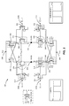
- FIG. 2 is a circuit diagram of an embodiment of a level shifter circuit.
- a level shifter 200 can be used as a single level shifter 100 of FIG. 1 .
- the level shifter 200 is operable to shift both positive supply (V DD ) and negative supply (V SS ) concurrently.
- V DD positive supply
- V SS negative supply
- the multiple level shifters 100 of FIG. 1 (and the exemplary Hubble level shifter) described above can be minimized and replaced by, for example, a single level shifting stage of the level shifter 200 .
- the level shifter 200 can shift the first logic domain 110 (e.g., 0V-0.8V) to the second logic domain 120 (e.g., ⁇ 0.4V-1.7V) in a single shifting stage (e.g., the level shifter 100 ). It should be appreciated that any voltage levels/values can be used for the level shifter 200 .
- the level shifter 200 can have four inputs or voltage supplies.
- the first voltage supply, a first high input 210 can receive an input voltage according to a digital signal S 1 .
- the signal S 1 can vary, for example, between a first high voltage V DD1 and a first low voltage V SS1 representing a 1 and a 0, for example.
- the high voltage V DD1 can be from the first logic domain 110 (e.g., 0.8V).
- the first high input 210 is shown as a first high input 210 a and a first high input 210 b . This can allow the first high input 210 a and the first high input 210 b to be separated on different components but receive the same input signal S 1 and voltage input (V DD1 ). They can be collectively referred to herein as the first high input 210 .
- the second voltage supply can receive an input voltage according to an inverse of the digital signal S 1 or S 1 (i.e., read “S 1 -bar”).
- the first low input 220 can thus receive the low voltage V SS1 from the first logic domain 110 (e.g., 0V). Similar to above, the first low input 220 is shown as a first low input 220 a and a first low input 220 b .
- the voltages or signals applied to the first high input 210 and the first low input 220 can be inverses of one another, or for example, the opposite digital value of each other.
- the digital signal S 1 can be provided to the first high input 210 while an inverse of the digital signal S 1 , or S 1 can be provided to the first low input 220 . Therefore the voltage value supplied to the first high input 210 can be the opposite digital value of the first low input 220 for the particular logic domain family.
- the third voltage supply, a second high input 230 can receive the high voltage for the second logic domain 120 (e.g., V DD2 , 1.7V).
- the high voltage from the second logic domain 120 may be referred to herein as V DD2 .
- the second high input 230 can also be referred to as a shifted input.
- the fourth voltage supply, a second low input 240 can receive the low voltage for the second logic domain 120 (e.g., ⁇ 0.4V).
- the low voltage for the second logic domain 120 may be referred to herein as V SS2 .
- the second low input 230 can also be referred to as a shifted input.
- the first high input 210 can be coupled to a gate of a first input switch 212 and a gate of a second input switch 214 .
- the first input switch 212 and the second input switch 214 can be coupled together at their respective gates.
- the first high input 210 can also be coupled to a gate of a first guard switch 216 and a gate of a second guard switch 218 .
- the first low input 220 can be coupled to a gate of a third input switch 222 and a gate of a fourth input switch 224 .
- the third input switch 222 and the fourth input switch 224 can be coupled together at their respective gates.
- the first low input 220 can also be coupled to a gate of a third guard switch 226 and a gate of a fourth guard switch 228 .
- the second high input 230 can be coupled to the sources of each of a first conversion switch 232 and a second conversion switch 234 .
- the sources of each of the first conversion switch 232 and the second conversion switch 234 can further be coupled to a respective bulk terminal, further connecting the bulk terminals to the second high input 230 .
- a drain of the first conversion switch 232 can be coupled to a source of the first guard switch 216 , a drain of the first input switch 212 , and a gate of the second conversion switch 234 at a node 236 .
- a drain of the second conversion switch 234 can be coupled to a source of the third guard switch 226 , a drain of the third input switch 222 , and a gate of the first conversion switch 232 at a node 238 .
- the connections of the first conversion switch 232 and the second conversion switch 234 can have a cross-coupled arrangement.
- the second low input 240 can be coupled to the sources of each of a third conversion switch 242 and a fourth conversion switch 244 .
- a drain of the third conversion switch 242 can be coupled to a drain of the second input switch 214 , a source of the second guard switch 218 , and a gate of the fourth conversion switch 244 at a node 246 .
- the drain of the fourth conversion switch 244 can be coupled to a drain of the fourth input switch 224 , a source of the fourth guard switch 228 , and the gate of the third conversion switch 242 and node 248 .
- the connections of the third conversion switch 242 and the fourth conversion switch 244 can have a cross-coupled arrangement.
- the first guard switch 216 , the second guard switch 218 , the third guard switch 226 , and the fourth guard switch 228 can be arranged between the cross-couplings of the various conversion switches as shown.
- the first guard switch 216 , the second guard switch 218 , the third guard switch 226 , and the fourth guard switch 228 can be disposed between the cross-coupling of the first conversion switch 232 and the second conversion switch 234 , and the cross-coupling of the third conversion switch 242 and the fourth conversion switch 244 .
- the first output 250 can be coupled to the drains of the first guard switch 216 and the second guard switch 218 while the second output 260 can be coupled to the to the drains of the third guard switch 226 and the fourth guard switch 228 .
- the input voltages from S 1 , or S 1 can be coupled to the gates of the guard switches and the first output 250 and the second output 260 can be coupled to the drains of the guard switches. This can provide an overvoltage protection to the other circuitry by preventing continuity between the second high input 230 and the second low input 240 .
- the third guard switch 218 , the fourth guard switch 228 , the third conversion switch 242 , and the fourth conversion switch 244 can be implemented as triple well devices.
- the triple well devices can have six total connections for a gate, a source, a drain, and three bulk terminals (e.g., B1, B2, B3).
- An exemplary triple well device is illustrated in a dot-dash box in FIG. 2 .
- Each of the bulk terminals can be configured as an N-well or a P-well bulk terminal.
- the triple well devices can eliminate certain reliability issues over three terminal or four terminal transistors, for example.
- the bulk terminal connections can be the same for each of the third guard switch 218 , the fourth guard switch 228 , the third conversion switch 242 , and the fourth conversion switch 244 .
- each of the triple well devices of the third guard switch 218 , the fourth guard switch 228 , the third conversion switch 242 , and the fourth conversion switch 244 can have B1 (P-well bulk) coupled to V SS1 , B2 (N-well bulk) coupled to V DD2 , and B3 (P-well bulk) coupled to V SS2 .
- these specific connections can provide certain advantages, reducing reliability and leakage issues associated with different transistor configurations (e.g., with three terminal and four terminal transistors).
- the remaining transistors (e.g., switches) of the level shifter 200 can be implemented as four terminal transistors (e.g., MOSFET) having a gate, a drain, a source, and a single bulk terminal.
- a source of the first input switch 212 and a source of the third input switch 222 can each be coupled to (e.g., receive) a voltage equivalent to the low voltage (V SS1 ) of the first logic domain 110 (e.g., 0V or ground).
- the sources of both of the first input switch 212 and the third input switch 222 can further be coupled to their respective bulk terminal (e.g., body terminal), so that the voltage V SS1 is also coupled to the bulk terminals.
- a source of the second input switch 214 and a source of the fourth input switch 224 can each be coupled to (e.g., to receive) the high voltage (V DD1 ) of the first logic domain 110 (e.g., 0.8V).
- the sources of both of the second input switch 214 and the fourth input switch 224 can further be coupled to their respective bulk terminal (e.g., body terminal), so that the voltage V DD1 is also coupled to the bulk terminals.
- a bulk terminal of each of the first guard switch 216 and the third guard switch 226 can each be coupled to the voltage V DD2 .
- the first high input 210 can receive the signal S 1 and the first low input 220 can receive S 1 , each having the first logic domain 110 ranging from, for example 0V to 0.8V.
- the various switches of the level shifter 200 can convert the first logic domain 110 to the second logic domain 120 at a first output 250 (V OUTP ) and a second output 260 (V OUTM ).
- the voltage value at the output 260 may generally be the opposite, in terms of the logic domain, of the voltage value at the output 250 .
- the first input switch 212 turns on, allowing the value of V SS1 (e.g., 0V) to be present at the node 236 and the gate of the second conversion switch 234 .
- the second conversion switch 234 is switched then also switched on, allowing the voltage V DD2 (e.g., 1.7V) at the second high input 230 to flow to the node 238 .
- the third guard switch 226 is switched on by the presence of the voltage V SS1 (e.g., 0V) at the first low input 120 (e.g., from S 1 ).
- the first input switch 212 , the second conversion switch 234 , the second guard switch 218 , the third guard switch 226 , the third conversion switch 242 , and the fourth input switch are all “ON” with V DD1 applied to the first high input 210 (and V SS1 applied to the first low input 220 ) as shown in dashed boxes.
- the second input switch 214 , the first guard switch 216 , the first conversion switch 232 , the third input switch 222 , and the fourth conversion switch 244 are all switched “OFF” in this instance.
- the OFF state of the first guard switch 216 and the fourth guard switch is indicated with a dashed circle.
- an “ON” state of one or more transistors, or switches can refer to a state in which the gate-to-source voltage is above threshold and transconductance from source-to-drain or drain-to-source of a respective transistor, or switch, is greater than zero.
- an “OFF” state can refer to a below-threshold state of a transistor, or switch, where transconductance is approximately zero, or at least negligible.
- the first low input 220 is low, receiving the voltage V SS1 because S 1 is present and the value is opposite the value of S 1 at the first high input 210 . Accordingly, the fourth input switch 224 , the third conversion switch 242 , and the third guard switch 226 are switched on, indicated with dashed boxes.
- the voltage V SS2 at the second low input 240 (e.g., ⁇ 0.4V) is then present at the first output 250 (shown with a dotted line).
- the first guard switch 216 and the fourth guard switch 228 are OFF.
- the position and bias of the first guard switch 216 and the fourth guard switch 228 can aid in preventing overvoltage of the various switches/transistors within the level shifter 200 .
- using the second logic domain 120 with negative ( ⁇ ) 0.4V to +1.7V results in a 2.1V voltage range.
- the first guard switch 216 and the fourth guard switch 228 prevent any of the transistors (switches) from encountering such a voltage range.
- FIG. 3 is a circuit diagram of an embodiment of the level shifter circuit of FIG. 2 .
- the arrangement shown in FIG. 3 is similar to that of FIG. 2 , showing the opposite digital value, the first low voltage V SS1 present at the first high input 210 . Because the S 1 is applied to the first low input 220 , the opposite the logic value, or the first high voltage V DD1 , is present.
- the first high input 210 receives the voltage V SS1 (e.g., 0V)
- the opposite switches from that of FIG. 2 are actuated (e.g., turned ON) providing the voltage V SS2 (e.g., ⁇ 0.4V) present at the second low input 240 to flow through fourth conversion switch 244 and the fourth guard switch 228 to the second output 260 .
- the ON states of the switches is indicated with dashed boxes.
- the voltage V DD2 e.g., +1.7V
- present at the second high input 230 can then flow through the first conversion switch 232 and the first guard switch 216 to the first output 150 .
- the first guard switch 216 and the fourth guard switch 228 are both OFF (show with dashed circles). This can prevent any single component of the level shifter 200 from being exposed to the full potential difference from the second high input 230 and the second low input 240 .
- the signal S 1 at the first high input 210 (and S 1 at the first low input 220 ), having the first logic domain 110 (e.g., 0V-0.8V) can be shifted to a signal S 2 at the second output 260 (and a signal S 2 at the first output 150 ) with the second logic domain 120 (e.g., ⁇ 0.4V-+1.7V)
- a current circuit (not shown) can be coupled to the second high input 230 and the second low input 240 to provide the second high voltage and the second low voltage, respectively.
- DSP digital signal processor
- ASIC application specific integrated circuit
- FPGA field programmable gate array
- a general-purpose processor can be a microprocessor, but in the alternative, the processor can be any processor, controller, microcontroller, or state machine.
- a processor can also be implemented as a combination of computing devices, for example, a combination of a DSP and a microprocessor, a plurality of microprocessors, one or more microprocessors in conjunction with a DSP core, or any other such configuration.
- a software module can reside in RAM memory, flash memory, ROM memory, EPROM memory, EEPROM memory, registers, hard disk, a removable disk, a CD-ROM, or any other form of storage medium.
- An exemplary storage medium can be coupled to the processor such that the processor can read information from, and write information to, the storage medium. In the alternative, the storage medium can be integral to the processor.
- the processor and the storage medium can reside in an ASIC.
Landscapes
- Engineering & Computer Science (AREA)
- Computer Hardware Design (AREA)
- Physics & Mathematics (AREA)
- Computing Systems (AREA)
- General Engineering & Computer Science (AREA)
- Mathematical Physics (AREA)
- Logic Circuits (AREA)
Abstract
A device and method for shifting voltage levels within a circuit are provided. An aspect of the disclosure provides a level shifting circuit for shifting a first logic domain to a second logic domain. In particular, the level shifting circuit can receive an input signal having a first logic domain with a first high voltage and a first low voltage. The level shifting circuit can receive inputs corresponding to a second high voltage and a second low voltage from the second logic domain. The level shifting circuit can concurrently switch the first high voltage and first low voltage at the input to the second high voltage and the second low voltage to produce a level-shifted version of the input signal at the output. The level shifting circuit can also have a plurality of guard transistors that prevent overvoltage of the circuit components.
Description
This disclosure relates to digital circuits and circuit design. More particularly, this disclosure relates to shifting voltage level requirements within digital circuits.
Digital circuits can use a consistent logic for internal signals, such as a digital 0 or 1, for example. The logic can be represented by discrete logic domains or voltage (V) values. Those logic domains, however, can vary from one system to another. Interconnecting any two systems or circuits having different logic families can require special interface circuits such as level shifters, for example.
A level shifter can couple one digital circuit using a first logic domain to another digital circuit that uses a second logic domain. For example, a first logic domain can use a negative (−) 0.5V to represent a digital 0 and a positive (+) 0.5V for a digital 1. A second logic domain can have a higher or lower second range of voltages (e.g., 0V and +1V, or +0.5 and +1.5) that may not be supported by the circuitry of the first digital circuit. The level shifter can translate the first logic domain to the second logic domain.
In some examples, the first logic domain and the second logic domain can require multiple stages of level shifters due to the difference in voltage values associated with the digital values. Therefore, level shifters can be cascaded, using two or more level shifters at once to change the first logic domain into a second. There can be one or more level shifters at each system operable to increase or decrease the voltage level of various logic families.
Some level shifters have significant reliability and leakage current issues, leading to unintended power drain and lower efficiency. In some examples, this can be caused by a large difference between the first logic domain and the second logic domain, overwhelming level shifter circuitry.
An aspect of the disclosure provides a level shifting circuit for shifting a first logic domain to a second logic domain. The level shifting circuit can have a first pair of cross-coupled transistors having sources coupled to a first voltage supply configured to receive a first voltage from the second logic domain. The level shifting circuit can also have a second pair of cross-coupled transistors having sources coupled to a second voltage supply configured to receive a second voltage from the second logic domain. The level shifting circuit can also have a first plurality of transistors having gates coupled to a third voltage supply. The first plurality of transistors can be coupled in series between a first transistor of the first pair and a first transistor of the second pair and further having a first output located between two transistors of the first plurality of transistors. The level shifting circuit can also have a second plurality of transistors having gates coupled to a fourth voltage supply. The second plurality of transistors can be coupled in series between a second transistor of the first pair and a second transistor of the second pair and further having a second output located between two transistors of the second plurality of transistors.
Another aspect of the disclosure provides a method for shifting a first logic domain to a second logic domain in an electrical circuit. The method can include receiving, at a first input switch and a second input switch, an input signal having the first logic domain. The first logic domain can have a first high voltage and a first low voltage. The method can also include receiving an inverted version of the input signal at a third input switch and a fourth input switch. The method can also include receiving a second high voltage from a second logic domain at a first conversion switch and a second conversion switch. The second logic domain can be different from the first logic domain. The method can also include receiving a second low voltage from the second logic domain at a third conversion switch and a fourth conversion switch. The method can also include first providing the second low voltage of the second logic domain to a first output. The method can also include second providing the second high voltage of the second logic domain to a second output concurrently with the first providing. The method can also include preventing, by a plurality of guard switches, any of the first conversion switch, the second conversion switch, the third conversion switch, and the fourth conversion switch from overvoltage during the first providing and the second providing.
Another aspect of the disclosure provides an apparatus for shifting a first logic domain to a second logic domain in an electrical circuit. The apparatus can have first receiving means for receiving an input signal having the first logic domain. The first logic domain can have a first high logic voltage and a first low logic voltage. The apparatus can also have second receiving means for receiving an inverted version of the input signal. The apparatus can also have first conversion means for receiving a second high logic voltage from a second logic domain different from the first logic domain. The apparatus can also have second conversion means for receiving a second low logic voltage from the second logic domain. The apparatus can also have first shifting means for first shifting the first high logic voltage of the first logic domain to the second high logic voltage of the second logic domain. The apparatus can also have second shifting means for second shifting the first low logic voltage of the first logic domain to the second low logic voltage of the second logic domain concurrently with the first shifting. The apparatus can also have preventing means for preventing any of the first receiving means, the second receiving means, the first conversion means, and the second means from overvoltage during the first shifting and the second shifting.
Another aspect of the disclosure provides a level shifting circuit for concurrently shifting a first high logic voltage and a first low logic voltage of a first logic domain, to a second high logic voltage and a second low logic voltage of a second logic domain. The second logic domain can be different from the first logic domain. The level shifting circuit can have a first portion. The first portion can have a first pair of input switches operable to receive an input signal from the first logic domain. The first portion can also have a first pair of conversion switches operable to receive voltages from the second logic family. The level shifting circuit can also have a second portion. The second portion can have a second pair of input switches operable to receive an inverted version of the input signal. The second portion can also have a second pair of conversion switches operable to receive voltages from the second logic family, the second portion coupled to the first portion at a second high input and a second low input. The level shifting circuit can also have a plurality of guard switches coupling the first portion to the second portion, and operable to prevent overvoltage of the first and second pair of conversion switches and the first and second pair of input switches. The level shifting circuit can also have a first output coupled to a portion of the plurality of guard switches operable to provide a shifted version of the input signal using the second logic family.
The details of embodiments of the present disclosure, both as to their structure and operation, may be gleaned in part by study of the accompanying drawings, in which like reference numerals refer to like parts, and in which:
The second circuit 122 can operate using the second logic domain 120 for 0 and 1. For example, the second logic domain 120 can have a different range of voltage levels than the first logic domain 110. In some embodiments, the second logic domain 120 can use a range of values VSS2-VDD2, for example, −0.4V for a digital zero and +1.8V for a digital one.
The second circuit 122 can operate using the second logic domain 120 for 0 and 1. For example, the second logic domain 120 can have a different range of voltage levels than the first logic domain 110. In some embodiments, the second logic domain 120 can use a range of values Vss1-Vdd1, for example, −0.4V for a digital zero and +1.8V for a digital one.
The level shifters 100 can implement N-type or P-type metal oxide semiconductors (MOS), or NMOS and PMOS, transistors as one or more switches in order to provide level shifting from the first logic domain 110 to the second logic domain 120. In some examples, NMOS switches having leakage currents can negatively affect power dissipation and the performance of the level shifters 100. Accordingly, in some embodiments (as described below), the NMOS switches can then be negatively biased below −0.4 volts. This arrangement can improve the ON-OFF switch resistance ratio of the NMOS transistors.
As shown in FIG. 1 , the level shifting circuit 10 may need to shift from the first logic domain 110 (e.g., using 0V to 0.8V) to the second logic domain 120 (e.g., using, −0.4V to 1.7V). This presents a 2.1V differential between high (1) and low (0) digital values. Such a voltage drop can, in some level shifters, create an overvoltage condition, damaging the circuit or causing it to fail due to reliability and leakage current issues. Thus, more than one level shifter 100 may be needed to shift the first logic domain 110 to the second logic domain 120. The one or more level shifters 100 may be needed because certain level shifting circuitry may not be able to operate at increased high-low voltage differentials.
In some examples the level shifting circuit 10 can shift the first logic domain 110 to an intermediate logic domain 115 using the level shifter 100 a, and then from the intermediate logic domain 115 to the second logic domain 120 using the second level shifter 100 b. For example, the level shifter 100 a can shift VDD1 to an intermediate value VDD before the level shifter 100 b can shift the intermediate VDD to VDD2 of the second logic domain 120. Some level shifting circuits 10 may only shift VDD1 to VDD2, ignoring VSS, or allowing VSS to remain at the voltage level defined by the first logic domain 110 (e.g., Vss1). This can limit level shifting capabilities of the level shifting circuit 10.
Certain cascaded level shifters 100 can require additional biasing circuitry, such as in a Hubble level shifter having three levels of shifting (e.g., three level shifters 100). In the Hubble level shifter, there are two level shifters 100 for supply level shifting from 1.0V to 1.8V and then from 1.8V to 1.3V (e.g., VDD1), and a third level shifter 100 for ground level shifting from 0V to negative (−)0.4V. This further assumes that the threshold voltage (Vth) of the NMOS is less than 0.4V, however that may not always be true across process and temperature variations in the transistors.
Some level shifters can have pairs of cross coupled transistors with the input transistors shielded from overvoltage by cascode devices. However, such a topology can require additional bias voltages for the cascade devices. In some embodiments where using large numbers of level shifters (e.g., 80-100 level shifters 100), power consumption under such conditions may be unacceptably high. Implementing a single level shifter 100 as disclosed herein can reduce space requirements and minimize power dissipation.
In some embodiments, the level shifter 200 can have four inputs or voltage supplies. The first voltage supply, a first high input 210, can receive an input voltage according to a digital signal S1. The signal S1 can vary, for example, between a first high voltage VDD1 and a first low voltage VSS1 representing a 1 and a 0, for example. The high voltage VDD1 can be from the first logic domain 110 (e.g., 0.8V). The first high input 210 is shown as a first high input 210 a and a first high input 210 b. This can allow the first high input 210 a and the first high input 210 b to be separated on different components but receive the same input signal S1 and voltage input (VDD1). They can be collectively referred to herein as the first high input 210.
The second voltage supply, a first low input 220, can receive an input voltage according to an inverse of the digital signal S1 or S1 (i.e., read “S1-bar”). The first low input 220 can thus receive the low voltage VSS1 from the first logic domain 110 (e.g., 0V). Similar to above, the first low input 220 is shown as a first low input 220 a and a first low input 220 b. The voltages or signals applied to the first high input 210 and the first low input 220 can be inverses of one another, or for example, the opposite digital value of each other. The digital signal S1 can be provided to the first high input 210 while an inverse of the digital signal S1, or S1 can be provided to the first low input 220. Therefore the voltage value supplied to the first high input 210 can be the opposite digital value of the first low input 220 for the particular logic domain family.
The third voltage supply, a second high input 230, can receive the high voltage for the second logic domain 120 (e.g., VDD2, 1.7V). The high voltage from the second logic domain 120 may be referred to herein as VDD2. The second high input 230 can also be referred to as a shifted input. The fourth voltage supply, a second low input 240, can receive the low voltage for the second logic domain 120 (e.g., −0.4V). The low voltage for the second logic domain 120 may be referred to herein as VSS2. The second low input 230 can also be referred to as a shifted input.
Multiple transistors can be arranged to provide switching for the conversion from the first logic domain (e.g., voltage range) to the second logic domain (e.g., voltage range). The first high input 210 can be coupled to a gate of a first input switch 212 and a gate of a second input switch 214. In some embodiments, the first input switch 212 and the second input switch 214 can be coupled together at their respective gates. The first high input 210 can also be coupled to a gate of a first guard switch 216 and a gate of a second guard switch 218.
The first low input 220 can be coupled to a gate of a third input switch 222 and a gate of a fourth input switch 224. In some embodiments, the third input switch 222 and the fourth input switch 224 can be coupled together at their respective gates. The first low input 220 can also be coupled to a gate of a third guard switch 226 and a gate of a fourth guard switch 228.
The second high input 230 can be coupled to the sources of each of a first conversion switch 232 and a second conversion switch 234. The sources of each of the first conversion switch 232 and the second conversion switch 234 can further be coupled to a respective bulk terminal, further connecting the bulk terminals to the second high input 230. A drain of the first conversion switch 232 can be coupled to a source of the first guard switch 216, a drain of the first input switch 212, and a gate of the second conversion switch 234 at a node 236. Similarly, a drain of the second conversion switch 234 can be coupled to a source of the third guard switch 226, a drain of the third input switch 222, and a gate of the first conversion switch 232 at a node 238. The connections of the first conversion switch 232 and the second conversion switch 234 can have a cross-coupled arrangement.
The second low input 240 can be coupled to the sources of each of a third conversion switch 242 and a fourth conversion switch 244. A drain of the third conversion switch 242 can be coupled to a drain of the second input switch 214, a source of the second guard switch 218, and a gate of the fourth conversion switch 244 at a node 246. Similarly, the drain of the fourth conversion switch 244 can be coupled to a drain of the fourth input switch 224, a source of the fourth guard switch 228, and the gate of the third conversion switch 242 and node 248. The connections of the third conversion switch 242 and the fourth conversion switch 244 can have a cross-coupled arrangement.
In some embodiments, the first guard switch 216, the second guard switch 218, the third guard switch 226, and the fourth guard switch 228 can be arranged between the cross-couplings of the various conversion switches as shown. Thus in some embodiments, the first guard switch 216, the second guard switch 218, the third guard switch 226, and the fourth guard switch 228 can be disposed between the cross-coupling of the first conversion switch 232 and the second conversion switch 234, and the cross-coupling of the third conversion switch 242 and the fourth conversion switch 244. Additionally, the first output 250 can be coupled to the drains of the first guard switch 216 and the second guard switch 218 while the second output 260 can be coupled to the to the drains of the third guard switch 226 and the fourth guard switch 228.
As noted above, the input voltages from S1, or S1 can be coupled to the gates of the guard switches and the first output 250 and the second output 260 can be coupled to the drains of the guard switches. This can provide an overvoltage protection to the other circuitry by preventing continuity between the second high input 230 and the second low input 240.
In some embodiments, the third guard switch 218, the fourth guard switch 228, the third conversion switch 242, and the fourth conversion switch 244 can be implemented as triple well devices. The triple well devices can have six total connections for a gate, a source, a drain, and three bulk terminals (e.g., B1, B2, B3). An exemplary triple well device is illustrated in a dot-dash box in FIG. 2 . Each of the bulk terminals can be configured as an N-well or a P-well bulk terminal. In some examples, the triple well devices can eliminate certain reliability issues over three terminal or four terminal transistors, for example.
The bulk terminal connections (e.g., for B1, B2, B3) can be the same for each of the third guard switch 218, the fourth guard switch 228, the third conversion switch 242, and the fourth conversion switch 244. For example, each of the triple well devices of the third guard switch 218, the fourth guard switch 228, the third conversion switch 242, and the fourth conversion switch 244 can have B1 (P-well bulk) coupled to VSS1, B2 (N-well bulk) coupled to VDD2, and B3 (P-well bulk) coupled to VSS2. In some implementations, these specific connections can provide certain advantages, reducing reliability and leakage issues associated with different transistor configurations (e.g., with three terminal and four terminal transistors).
In such embodiments, the remaining transistors (e.g., switches) of the level shifter 200 can be implemented as four terminal transistors (e.g., MOSFET) having a gate, a drain, a source, and a single bulk terminal. A source of the first input switch 212 and a source of the third input switch 222 can each be coupled to (e.g., receive) a voltage equivalent to the low voltage (VSS1) of the first logic domain 110 (e.g., 0V or ground). The sources of both of the first input switch 212 and the third input switch 222 can further be coupled to their respective bulk terminal (e.g., body terminal), so that the voltage VSS1 is also coupled to the bulk terminals.
A source of the second input switch 214 and a source of the fourth input switch 224 can each be coupled to (e.g., to receive) the high voltage (VDD1) of the first logic domain 110 (e.g., 0.8V). The sources of both of the second input switch 214 and the fourth input switch 224 can further be coupled to their respective bulk terminal (e.g., body terminal), so that the voltage VDD1 is also coupled to the bulk terminals.
A bulk terminal of each of the first guard switch 216 and the third guard switch 226 can each be coupled to the voltage VDD2.
The first high input 210 can receive the signal S1 and the first low input 220 can receive S1 , each having the first logic domain 110 ranging from, for example 0V to 0.8V. As the voltage at the first high input 210 and the first low input 220 switch from high (VDD1) to low (VSS1) and back, the various switches of the level shifter 200 can convert the first logic domain 110 to the second logic domain 120 at a first output 250 (VOUTP) and a second output 260 (VOUTM). The voltage value at the output 260 may generally be the opposite, in terms of the logic domain, of the voltage value at the output 250.
For example, if the signal S1 at the first high input 210 is high (e.g., 0.8V), the first input switch 212 turns on, allowing the value of VSS1 (e.g., 0V) to be present at the node 236 and the gate of the second conversion switch 234. The second conversion switch 234 is switched then also switched on, allowing the voltage VDD2 (e.g., 1.7V) at the second high input 230 to flow to the node 238. The third guard switch 226 is switched on by the presence of the voltage VSS1 (e.g., 0V) at the first low input 120 (e.g., from S1 ). This provides the voltage VDD2 at the second high input 230 to the second output 260. The first input switch 212, the second conversion switch 234, the second guard switch 218, the third guard switch 226, the third conversion switch 242, and the fourth input switch are all “ON” with VDD1 applied to the first high input 210 (and VSS1 applied to the first low input 220) as shown in dashed boxes. The second input switch 214, the first guard switch 216, the first conversion switch 232, the third input switch 222, and the fourth conversion switch 244 are all switched “OFF” in this instance. The OFF state of the first guard switch 216 and the fourth guard switch is indicated with a dashed circle. As used herein, an “ON” state of one or more transistors, or switches, can refer to a state in which the gate-to-source voltage is above threshold and transconductance from source-to-drain or drain-to-source of a respective transistor, or switch, is greater than zero. As used herein, an “OFF” state can refer to a below-threshold state of a transistor, or switch, where transconductance is approximately zero, or at least negligible.
On the other side of the level shifter 200, the first low input 220 is low, receiving the voltage VSS1 because S1 is present and the value is opposite the value of S1 at the first high input 210. Accordingly, the fourth input switch 224, the third conversion switch 242, and the third guard switch 226 are switched on, indicated with dashed boxes. The voltage VSS2 at the second low input 240 (e.g., −0.4V) is then present at the first output 250 (shown with a dotted line).
In some embodiments, with the voltage VDD1 (e.g., 0.8V) at the first high input 210 and the voltage VSS1 (e.g., 0.0V) at the first low input 220, the first guard switch 216 and the fourth guard switch 228 are OFF. The position and bias of the first guard switch 216 and the fourth guard switch 228 can aid in preventing overvoltage of the various switches/transistors within the level shifter 200. For example, using the second logic domain 120 with negative (−) 0.4V to +1.7V results in a 2.1V voltage range. If such a voltage was applied across a single switch (e.g., the conversion switches) within the level shifter 200, they may be damaged by exceeding the maximum gate-to-source voltage (Vgs) or drain-to-source voltage (Vds) of a given circuit component. In this example, the first guard switch 216 and the fourth guard switch 228 prevent any of the transistors (switches) from encountering such a voltage range.
Therefore, when the signal S1 is low, the first high input 210 receives the voltage VSS1 (e.g., 0V), the opposite switches from that of FIG. 2 are actuated (e.g., turned ON) providing the voltage VSS2 (e.g., −0.4V) present at the second low input 240 to flow through fourth conversion switch 244 and the fourth guard switch 228 to the second output 260. The ON states of the switches is indicated with dashed boxes. Similarly, the voltage VDD2 (e.g., +1.7V) present at the second high input 230 can then flow through the first conversion switch 232 and the first guard switch 216 to the first output 150.
In the same instant, the first guard switch 216 and the fourth guard switch 228 are both OFF (show with dashed circles). This can prevent any single component of the level shifter 200 from being exposed to the full potential difference from the second high input 230 and the second low input 240.
Thus, for example, the signal S1 at the first high input 210 (and S1 at the first low input 220), having the first logic domain 110 (e.g., 0V-0.8V) can be shifted to a signal S2 at the second output 260 (and a signal S2 at the first output 150) with the second logic domain 120 (e.g., −0.4V-+1.7V)
In some embodiments, a current circuit (not shown) can be coupled to the second high input 230 and the second low input 240 to provide the second high voltage and the second low voltage, respectively. Given the guard switches and the arrangement of the conversion switches, there is no need for additional biasing circuits. This arrangement further eliminates excessive leakage current and minimizes the number of transistors required also minimizing the size of the circuit.
Those of skill will appreciate that the various illustrative blocks described in connection with the embodiments disclosed herein can be implemented in various forms. Some blocks have been described above generally in terms of their functionality. How such functionality is implemented depends upon the design constraints imposed on an overall system. Skilled persons can implement the described functionality in varying ways for each particular application, but such implementation decisions should not be interpreted as causing a departure from the scope of the disclosure. In addition, the grouping of functions within a block or step is for ease of description. Specific functions or steps can be moved from one block or distributed across to blocks without departing from the present disclosure.
The various illustrative logical blocks described in connection with the embodiments disclosed herein, can be implemented or performed with a general purpose processor, a digital signal processor (DSP), application specific integrated circuit (ASIC), a field programmable gate array (FPGA) or other programmable logic device, discrete gate or transistor logic, discrete hardware components, or any combination thereof designed to perform the functions described herein. A general-purpose processor can be a microprocessor, but in the alternative, the processor can be any processor, controller, microcontroller, or state machine. A processor can also be implemented as a combination of computing devices, for example, a combination of a DSP and a microprocessor, a plurality of microprocessors, one or more microprocessors in conjunction with a DSP core, or any other such configuration.
The steps of a method described in connection with the embodiments disclosed herein can be embodied directly in hardware, in a software module executed by a processor, or in a combination of the two. A software module can reside in RAM memory, flash memory, ROM memory, EPROM memory, EEPROM memory, registers, hard disk, a removable disk, a CD-ROM, or any other form of storage medium. An exemplary storage medium can be coupled to the processor such that the processor can read information from, and write information to, the storage medium. In the alternative, the storage medium can be integral to the processor. The processor and the storage medium can reside in an ASIC.
The above description of the disclosed embodiments is provided to enable any person skilled in the art to make or use the present disclosure. Various modifications to these embodiments will be readily apparent to those skilled in the art, and the generic principles described herein can be applied to other embodiments without departing from the spirit or scope of the present disclosure. Thus, it is to be understood that the description and drawings presented herein represent a presently preferred embodiment of the present disclosure and are therefore representative of the subject matter which is broadly contemplated by the present disclosure. It is further understood that the scope of the present disclosure fully encompasses other embodiments that may become obvious to those skilled in the art and that the scope of the present disclosure is accordingly limited by nothing other than the appended claims.
Claims (16)
1. A level shifting circuit for shifting a first logic domain to a second logic domain, the level shifting circuit comprising:
a first pair of cross-coupled transistors having sources coupled to a first voltage supply configured to receive a first voltage from the second logic domain and each transistor of the first pair of cross-coupled transistors having its gate directly coupled to the drain of the opposite transistor of the first pair of cross-coupled transistors;
a second pair of cross-coupled transistors having sources coupled to a second voltage supply configured to receive a second voltage from the second logic domain and each transistor of the second pair of cross-coupled transistors having its gate directly coupled to the drain of the opposite transistor of the second pair of cross-coupled transistors;
a first plurality of transistors having gates coupled to a third voltage supply, the first plurality of transistors coupled in series between a first transistor of the first pair and a first transistor of the second pair and further having a first output located between two transistors of the first plurality of transistors;
a second plurality of transistors having gates coupled to a fourth voltage supply, the second plurality of transistors coupled in series between a second transistor of the first pair and a second transistor of the second pair and further having a second output located between two transistors of the second plurality of transistors; and
wherein a signal at the fourth voltage supply comprises an inverted logic level of a logic level of the signal at the third voltage supply.
2. The level shifting circuit of claim 1 , wherein the first pair of cross-coupled transistors is coupled between the first voltage supply and the first plurality of transistors; and
wherein the second pair of cross-coupled transistors is coupled between the second voltage supply and the second plurality of transistors.
3. The level shifting circuit of claim 1 , wherein a first output voltage of the first output is at a different voltage level than a second output voltage at the second output.
4. The level shifting circuit of claim 3 , wherein the first pair of cross-coupled transistors is configured to level shift a voltage at the third voltage supply to the first output voltage; and
wherein the second pair of cross-coupled transistors are configured to level shift a voltage at the fourth voltage supply to the second output voltage concurrently with the first output voltage.
5. The level shifting circuit of claim 2 wherein the first plurality of transistors comprises a first guard switch and a second guard switch and the second plurality of transistors comprises a third guard switch and a fourth guard switch, and
wherein the first output is coupled to a drain of the first guard switch and a drain of the second guard switch, and the second output is coupled to a drain of the third guard switch and a drain of the fourth guard switch.
6. The level shifting circuit of claim 1 wherein the first voltage comprises 1.7 volts and the second voltage comprises negative 0.4 volts.
7. The level shifting circuit of claim 1 wherein the second pair, at least one transistor of the first plurality, and at least one transistor of the second plurality comprise triple well devices.
8. The level shifting circuit of claim 1 wherein the first plurality of transistors and the second plurality of transistors are configured to prevent overvoltage of the first pair and the second pair, wherein overvoltage comprises a potential difference of greater than 1.5 volts from gate-to-source or drain-to-source across any one of the first pair and the second pair.
9. A level shifting circuit for shifting a first logic domain to a second logic domain, the level shifting circuit comprising:
a first pair of cross-coupled transistors having sources coupled to a first voltage supply configured to receive a first voltage from the second logic domain and each transistor of the first pair of cross-coupled transistors having its gate directly coupled to the drain of the opposite transistor of the first pair of cross-coupled transistors;
a second pair of cross-coupled transistors having sources coupled to a second voltage supply configured to receive a second voltage from the second logic domain and each transistor of the second pair of cross-coupled transistors having its gate directly coupled to the drain of the opposite transistor of the second pair of cross-coupled transistors;
a first plurality of transistors having gates coupled to a third voltage supply, the first plurality of transistors coupled in series between a first transistor of the first pair and a first transistor of the second pair and further having a first output located between two transistors of the first plurality of transistors;
a second plurality of transistors having gates coupled to a fourth voltage supply, the second plurality of transistors coupled in series between a second transistor of the first pair and a second transistor of the second pair and further having a second output located between two transistors of the second plurality of transistors; and
wherein the second pair, at least one transistor of the first plurality, and at least one transistor of the second plurality comprise triple well devices.
10. The level shifting circuit of claim 9 , wherein the first pair of cross-coupled transistors is coupled between the first voltage supply and the first plurality of transistors; and
wherein the second pair of cross-coupled transistors is coupled between the second voltage supply and the second plurality of transistors.
11. The level shifting circuit of claim 9 , wherein a signal at the fourth voltage supply comprises an inverted logic level of a logic level of the signal at the third voltage supply.
12. The level shifting circuit of claim 9 , wherein a first output voltage of the first output is at a different voltage level than a second output voltage at the second output.
13. The level shifting circuit of claim 12 , wherein the first pair of cross-coupled transistors is configured to level shift a voltage at the third voltage supply to the first output voltage; and
wherein the second pair of cross-coupled transistors are configured to level shift a voltage at the fourth voltage supply to the second output voltage concurrently with the first output voltage.
14. The level shifting circuit of claim 10 wherein the first plurality of transistors comprises a first guard switch and a second guard switch and the second plurality of transistors comprises a third guard switch and a fourth guard switch, and
wherein the first output is coupled to a drain of the first guard switch and a drain of the second guard switch, and the second output is coupled to a drain of the third guard switch and a drain of the fourth guard switch.
15. The level shifting circuit of claim 9 wherein the first voltage comprises 1.7 volts and the second voltage comprises negative 0.4 volts.
16. The level shifting circuit of claim 9 wherein the first plurality of transistors and the second plurality of transistors are configured to prevent overvoltage of the first pair and the second pair, wherein overvoltage comprises a potential difference of greater than 1.5 volts from gate-to-source or drain-to-source across any one of the first pair and the second pair.
Priority Applications (4)
| Application Number | Priority Date | Filing Date | Title |
|---|---|---|---|
| US15/441,750 US10164637B2 (en) | 2017-02-24 | 2017-02-24 | Level shifter for voltage conversion |
| CN201880013449.8A CN110326217A (en) | 2017-02-24 | 2018-01-16 | Level shifter for voltage conversion |
| PCT/US2018/013869 WO2018156261A1 (en) | 2017-02-24 | 2018-01-16 | Level shifter for voltage conversion |
| EP18713041.4A EP3586442A1 (en) | 2017-02-24 | 2018-01-16 | Level shifter for voltage conversion |
Applications Claiming Priority (1)
| Application Number | Priority Date | Filing Date | Title |
|---|---|---|---|
| US15/441,750 US10164637B2 (en) | 2017-02-24 | 2017-02-24 | Level shifter for voltage conversion |
Publications (2)
| Publication Number | Publication Date |
|---|---|
| US20180248551A1 US20180248551A1 (en) | 2018-08-30 |
| US10164637B2 true US10164637B2 (en) | 2018-12-25 |
Family
ID=61764093
Family Applications (1)
| Application Number | Title | Priority Date | Filing Date |
|---|---|---|---|
| US15/441,750 Active US10164637B2 (en) | 2017-02-24 | 2017-02-24 | Level shifter for voltage conversion |
Country Status (4)
| Country | Link |
|---|---|
| US (1) | US10164637B2 (en) |
| EP (1) | EP3586442A1 (en) |
| CN (1) | CN110326217A (en) |
| WO (1) | WO2018156261A1 (en) |
Families Citing this family (5)
| Publication number | Priority date | Publication date | Assignee | Title |
|---|---|---|---|---|
| US10911047B1 (en) * | 2020-01-15 | 2021-02-02 | Qualcomm Incorporated | Level shifter with auto voltage-bias reliability protection |
| KR20210101566A (en) * | 2020-02-10 | 2021-08-19 | 삼성전자주식회사 | Level shifter circuitry and electronic apparatus including the same |
| US11171649B1 (en) * | 2020-10-15 | 2021-11-09 | Qualcomm Incorporated | Static and intermittent dynamic multi-bias core for dual pad voltage level shifter |
| US20230299762A1 (en) * | 2022-03-15 | 2023-09-21 | Faraday Technology Corporation | Level shifter and electronic device |
| CN119788058B (en) * | 2025-03-12 | 2025-06-24 | 上海芯炽集成电路技术有限公司 | A level conversion circuit |
Citations (11)
| Publication number | Priority date | Publication date | Assignee | Title |
|---|---|---|---|---|
| US5963054A (en) | 1997-12-05 | 1999-10-05 | Lucent Technologies Inc. | High voltage CMOS logic circuit using low voltage transistors |
| US5969542A (en) * | 1997-05-21 | 1999-10-19 | Advanced Micro Devices, Inc. | High speed gate oxide protected level shifter |
| US7167027B2 (en) | 2002-04-24 | 2007-01-23 | Fujitsu Limited | Latch-type level converter and receiver circuit accurately amplifying low-amplitude signals and receiving common-mode input signals higher than a supply voltage |
| US7696804B2 (en) * | 2007-03-31 | 2010-04-13 | Sandisk 3D Llc | Method for incorporating transistor snap-back protection in a level shifter circuit |
| US20100134146A1 (en) | 2008-12-03 | 2010-06-03 | Micron Technology, Inc. | Voltage level translator and method |
| US20100188131A1 (en) | 2009-01-23 | 2010-07-29 | Shayan Zhang | Level shifter for change of both high and low voltage |
| US8395433B2 (en) | 2009-04-20 | 2013-03-12 | Arm Limited | Input-output device protection |
| US8659341B2 (en) | 2011-05-02 | 2014-02-25 | Analog Devices, Inc. | System and method for level-shifting voltage signals using a dynamic level-shifting architecture |
| US8854104B2 (en) * | 2012-12-31 | 2014-10-07 | Taiwan Semiconductor Manufacturing Company, Ltd. | Voltage level shifter |
| US20160142056A1 (en) | 2014-11-14 | 2016-05-19 | Raydium Semiconductor Corporation | Level shifter of driving circuit |
| US9373275B2 (en) | 2013-10-04 | 2016-06-21 | Raydium Semiconductor Corporation | Level shifter of driving circuit and operating method thereof |
Family Cites Families (4)
| Publication number | Priority date | Publication date | Assignee | Title |
|---|---|---|---|---|
| EP2132873B1 (en) * | 2007-03-31 | 2012-08-22 | Sandisk 3D LLC | Level shifter circuit incorporating transistor snap-back protection |
| KR20100079331A (en) * | 2008-12-31 | 2010-07-08 | 주식회사 동부하이텍 | Level shifting circuit |
| US7804350B1 (en) * | 2009-04-22 | 2010-09-28 | Semiconductor Components Industries, Llc | Level shifting using cross-coupled cascode transistors |
| US9484922B2 (en) * | 2014-04-10 | 2016-11-01 | Freescale Semiconductor, Inc. | Voltage level shifter module |
-
2017
- 2017-02-24 US US15/441,750 patent/US10164637B2/en active Active
-
2018
- 2018-01-16 WO PCT/US2018/013869 patent/WO2018156261A1/en not_active Ceased
- 2018-01-16 EP EP18713041.4A patent/EP3586442A1/en not_active Withdrawn
- 2018-01-16 CN CN201880013449.8A patent/CN110326217A/en active Pending
Patent Citations (11)
| Publication number | Priority date | Publication date | Assignee | Title |
|---|---|---|---|---|
| US5969542A (en) * | 1997-05-21 | 1999-10-19 | Advanced Micro Devices, Inc. | High speed gate oxide protected level shifter |
| US5963054A (en) | 1997-12-05 | 1999-10-05 | Lucent Technologies Inc. | High voltage CMOS logic circuit using low voltage transistors |
| US7167027B2 (en) | 2002-04-24 | 2007-01-23 | Fujitsu Limited | Latch-type level converter and receiver circuit accurately amplifying low-amplitude signals and receiving common-mode input signals higher than a supply voltage |
| US7696804B2 (en) * | 2007-03-31 | 2010-04-13 | Sandisk 3D Llc | Method for incorporating transistor snap-back protection in a level shifter circuit |
| US20100134146A1 (en) | 2008-12-03 | 2010-06-03 | Micron Technology, Inc. | Voltage level translator and method |
| US20100188131A1 (en) | 2009-01-23 | 2010-07-29 | Shayan Zhang | Level shifter for change of both high and low voltage |
| US8395433B2 (en) | 2009-04-20 | 2013-03-12 | Arm Limited | Input-output device protection |
| US8659341B2 (en) | 2011-05-02 | 2014-02-25 | Analog Devices, Inc. | System and method for level-shifting voltage signals using a dynamic level-shifting architecture |
| US8854104B2 (en) * | 2012-12-31 | 2014-10-07 | Taiwan Semiconductor Manufacturing Company, Ltd. | Voltage level shifter |
| US9373275B2 (en) | 2013-10-04 | 2016-06-21 | Raydium Semiconductor Corporation | Level shifter of driving circuit and operating method thereof |
| US20160142056A1 (en) | 2014-11-14 | 2016-05-19 | Raydium Semiconductor Corporation | Level shifter of driving circuit |
Non-Patent Citations (3)
| Title |
|---|
| International Search Report and Written Opinion-PCT/US2018/013869-ISA/EPO-dated Jun. 18, 2018. |
| International Search Report and Written Opinion—PCT/US2018/013869—ISA/EPO—dated Jun. 18, 2018. |
| Khorasani M., et al., "Low-Power Static and Dynamic High-Voltage CMOS Level-Shifter Circuits", IEEE, International Symposium on Circuits and Systems, 2008, pp. 1946-1949. |
Also Published As
| Publication number | Publication date |
|---|---|
| WO2018156261A1 (en) | 2018-08-30 |
| CN110326217A (en) | 2019-10-11 |
| US20180248551A1 (en) | 2018-08-30 |
| EP3586442A1 (en) | 2020-01-01 |
Similar Documents
| Publication | Publication Date | Title |
|---|---|---|
| US10164637B2 (en) | Level shifter for voltage conversion | |
| US7683668B1 (en) | Level shifter | |
| US6064229A (en) | Voltage translating buffer based on low voltage technology | |
| US7102410B2 (en) | High voltage level converter using low voltage devices | |
| JP2011015402A (en) | Voltage level shifter | |
| CN109327218B (en) | Level shift circuit and integrated circuit chip | |
| CN107810421B (en) | Voltage monitor | |
| US20190214983A1 (en) | Clock voltage step-up circuit | |
| CN107786190A (en) | A kind of low on-resistance flatness analog switch with leakage current technology for eliminating | |
| US10209723B2 (en) | Low-voltage differential signaling driving circuit | |
| US7755392B1 (en) | Level shift circuit without high voltage stress of transistors and operating at low voltages | |
| CN109698688B (en) | inverter | |
| CN105897246B (en) | Voltage level shifter for high voltage applications | |
| US7064609B1 (en) | High voltage, low-offset operational amplifier with rail-to-rail common mode input range in a digital CMOS process | |
| EP2011236A2 (en) | Electronic circuit | |
| CN114389595B (en) | Level conversion circuit | |
| CN119892058A (en) | Wide-input-range low-power-consumption level shift circuit | |
| US9374047B2 (en) | Buffer circuit | |
| JP2017147560A (en) | Level shift circuit | |
| US10601405B2 (en) | Buffer circuit | |
| JP4588436B2 (en) | Level shifter circuit | |
| CN113708746B (en) | Analog switch circuit and multiplexer | |
| US8723581B1 (en) | Input buffers | |
| US8228115B1 (en) | Circuit for biasing a well from three voltages | |
| US12592682B1 (en) | Voltage scalable level shifter |
Legal Events
| Date | Code | Title | Description |
|---|---|---|---|
| AS | Assignment |
Owner name: QUALCOMM INCORPORATED, CALIFORNIA Free format text: ASSIGNMENT OF ASSIGNORS INTEREST;ASSIGNORS:MALLIA, SREENIVASA;MITTAL, AYUSH;THIAGARAJAN, KRISHNASWAMY;AND OTHERS;SIGNING DATES FROM 20170328 TO 20170414;REEL/FRAME:042324/0086 |
|
| STCF | Information on status: patent grant |
Free format text: PATENTED CASE |
|
| MAFP | Maintenance fee payment |
Free format text: PAYMENT OF MAINTENANCE FEE, 4TH YEAR, LARGE ENTITY (ORIGINAL EVENT CODE: M1551); ENTITY STATUS OF PATENT OWNER: LARGE ENTITY Year of fee payment: 4 |