US10152863B2 - Dual communication frequency RFID circuit equipped with a tamper-evident loop - Google Patents
Dual communication frequency RFID circuit equipped with a tamper-evident loop Download PDFInfo
- Publication number
- US10152863B2 US10152863B2 US15/831,444 US201715831444A US10152863B2 US 10152863 B2 US10152863 B2 US 10152863B2 US 201715831444 A US201715831444 A US 201715831444A US 10152863 B2 US10152863 B2 US 10152863B2
- Authority
- US
- United States
- Prior art keywords
- low
- pass filter
- linked
- rfid circuit
- resistor
- Prior art date
- Legal status (The legal status is an assumption and is not a legal conclusion. Google has not performed a legal analysis and makes no representation as to the accuracy of the status listed.)
- Active
Links
Images


Classifications
-
- G—PHYSICS
- G06—COMPUTING OR CALCULATING; COUNTING
- G06K—GRAPHICAL DATA READING; PRESENTATION OF DATA; RECORD CARRIERS; HANDLING RECORD CARRIERS
- G06K19/00—Record carriers for use with machines and with at least a part designed to carry digital markings
- G06K19/06—Record carriers for use with machines and with at least a part designed to carry digital markings characterised by the kind of the digital marking, e.g. shape, nature, code
- G06K19/067—Record carriers with conductive marks, printed circuits or semiconductor circuit elements, e.g. credit or identity cards also with resonating or responding marks without active components
- G06K19/07—Record carriers with conductive marks, printed circuits or semiconductor circuit elements, e.g. credit or identity cards also with resonating or responding marks without active components with integrated circuit chips
- G06K19/077—Constructional details, e.g. mounting of circuits in the carrier
- G06K19/07749—Constructional details, e.g. mounting of circuits in the carrier the record carrier being capable of non-contact communication, e.g. constructional details of the antenna of a non-contact smart card
-
- G—PHYSICS
- G06—COMPUTING OR CALCULATING; COUNTING
- G06K—GRAPHICAL DATA READING; PRESENTATION OF DATA; RECORD CARRIERS; HANDLING RECORD CARRIERS
- G06K7/00—Methods or arrangements for sensing record carriers, e.g. for reading patterns
- G06K7/0013—Methods or arrangements for sensing record carriers, e.g. for reading patterns by galvanic contacts, e.g. card connectors for ISO-7816 compliant smart cards or memory cards, e.g. SD card readers
- G06K7/0086—Methods or arrangements for sensing record carriers, e.g. for reading patterns by galvanic contacts, e.g. card connectors for ISO-7816 compliant smart cards or memory cards, e.g. SD card readers the connector comprising a circuit for steering the operations of the card connector
- G06K7/0091—Methods or arrangements for sensing record carriers, e.g. for reading patterns by galvanic contacts, e.g. card connectors for ISO-7816 compliant smart cards or memory cards, e.g. SD card readers the connector comprising a circuit for steering the operations of the card connector the circuit comprising an arrangement for avoiding intrusions and unwanted access to data inside of the connector
-
- G—PHYSICS
- G08—SIGNALLING
- G08B—SIGNALLING SYSTEMS, e.g. PERSONAL CALLING SYSTEMS; ORDER TELEGRAPHS; ALARM SYSTEMS
- G08B13/00—Burglar, theft or intruder alarms
- G08B13/22—Electrical actuation
- G08B13/24—Electrical actuation by interference with electromagnetic field distribution
- G08B13/2402—Electronic Article Surveillance [EAS], i.e. systems using tags for detecting removal of a tagged item from a secure area, e.g. tags for detecting shoplifting
- G08B13/2428—Tag details
- G08B13/2448—Tag with at least dual detection means, e.g. combined inductive and ferromagnetic tags, dual frequencies within a single technology, tampering detection or signalling means on the tag
-
- G—PHYSICS
- G06—COMPUTING OR CALCULATING; COUNTING
- G06K—GRAPHICAL DATA READING; PRESENTATION OF DATA; RECORD CARRIERS; HANDLING RECORD CARRIERS
- G06K19/00—Record carriers for use with machines and with at least a part designed to carry digital markings
- G06K19/06—Record carriers for use with machines and with at least a part designed to carry digital markings characterised by the kind of the digital marking, e.g. shape, nature, code
- G06K19/067—Record carriers with conductive marks, printed circuits or semiconductor circuit elements, e.g. credit or identity cards also with resonating or responding marks without active components
- G06K19/07—Record carriers with conductive marks, printed circuits or semiconductor circuit elements, e.g. credit or identity cards also with resonating or responding marks without active components with integrated circuit chips
- G06K19/073—Special arrangements for circuits, e.g. for protecting identification code in memory
- G06K19/07309—Means for preventing undesired reading or writing from or onto record carriers
- G06K19/07372—Means for preventing undesired reading or writing from or onto record carriers by detecting tampering with the circuit
- G06K19/07381—Means for preventing undesired reading or writing from or onto record carriers by detecting tampering with the circuit with deactivation or otherwise incapacitation of at least a part of the circuit upon detected tampering
-
- G—PHYSICS
- G06—COMPUTING OR CALCULATING; COUNTING
- G06K—GRAPHICAL DATA READING; PRESENTATION OF DATA; RECORD CARRIERS; HANDLING RECORD CARRIERS
- G06K19/00—Record carriers for use with machines and with at least a part designed to carry digital markings
- G06K19/06—Record carriers for use with machines and with at least a part designed to carry digital markings characterised by the kind of the digital marking, e.g. shape, nature, code
- G06K19/067—Record carriers with conductive marks, printed circuits or semiconductor circuit elements, e.g. credit or identity cards also with resonating or responding marks without active components
- G06K19/07—Record carriers with conductive marks, printed circuits or semiconductor circuit elements, e.g. credit or identity cards also with resonating or responding marks without active components with integrated circuit chips
- G06K19/0716—Record carriers with conductive marks, printed circuits or semiconductor circuit elements, e.g. credit or identity cards also with resonating or responding marks without active components with integrated circuit chips at least one of the integrated circuit chips comprising a sensor or an interface to a sensor
-
- G—PHYSICS
- G06—COMPUTING OR CALCULATING; COUNTING
- G06K—GRAPHICAL DATA READING; PRESENTATION OF DATA; RECORD CARRIERS; HANDLING RECORD CARRIERS
- G06K19/00—Record carriers for use with machines and with at least a part designed to carry digital markings
- G06K19/06—Record carriers for use with machines and with at least a part designed to carry digital markings characterised by the kind of the digital marking, e.g. shape, nature, code
- G06K19/067—Record carriers with conductive marks, printed circuits or semiconductor circuit elements, e.g. credit or identity cards also with resonating or responding marks without active components
- G06K19/07—Record carriers with conductive marks, printed circuits or semiconductor circuit elements, e.g. credit or identity cards also with resonating or responding marks without active components with integrated circuit chips
- G06K19/0723—Record carriers with conductive marks, printed circuits or semiconductor circuit elements, e.g. credit or identity cards also with resonating or responding marks without active components with integrated circuit chips the record carrier comprising an arrangement for non-contact communication, e.g. wireless communication circuits on transponder cards, non-contact smart cards or RFIDs
- G06K19/0724—Record carriers with conductive marks, printed circuits or semiconductor circuit elements, e.g. credit or identity cards also with resonating or responding marks without active components with integrated circuit chips the record carrier comprising an arrangement for non-contact communication, e.g. wireless communication circuits on transponder cards, non-contact smart cards or RFIDs the arrangement being a circuit for communicating at a plurality of frequencies, e.g. for managing time multiplexed communication over at least two antennas of different types
-
- G—PHYSICS
- G06—COMPUTING OR CALCULATING; COUNTING
- G06K—GRAPHICAL DATA READING; PRESENTATION OF DATA; RECORD CARRIERS; HANDLING RECORD CARRIERS
- G06K7/00—Methods or arrangements for sensing record carriers, e.g. for reading patterns
- G06K7/08—Methods or arrangements for sensing record carriers, e.g. for reading patterns by means detecting the change of an electrostatic or magnetic field, e.g. by detecting change of capacitance between electrodes
- G06K7/082—Methods or arrangements for sensing record carriers, e.g. for reading patterns by means detecting the change of an electrostatic or magnetic field, e.g. by detecting change of capacitance between electrodes using inductive or magnetic sensors
- G06K7/083—Methods or arrangements for sensing record carriers, e.g. for reading patterns by means detecting the change of an electrostatic or magnetic field, e.g. by detecting change of capacitance between electrodes using inductive or magnetic sensors inductive
- G06K7/086—Methods or arrangements for sensing record carriers, e.g. for reading patterns by means detecting the change of an electrostatic or magnetic field, e.g. by detecting change of capacitance between electrodes using inductive or magnetic sensors inductive sensing passive circuit, e.g. resonant circuit transponders
-
- G—PHYSICS
- G08—SIGNALLING
- G08B—SIGNALLING SYSTEMS, e.g. PERSONAL CALLING SYSTEMS; ORDER TELEGRAPHS; ALARM SYSTEMS
- G08B13/00—Burglar, theft or intruder alarms
- G08B13/02—Mechanical actuation
- G08B13/12—Mechanical actuation by the breaking or disturbance of stretched cords or wires
- G08B13/126—Mechanical actuation by the breaking or disturbance of stretched cords or wires for a housing, e.g. a box, a safe, or a room
-
- G—PHYSICS
- G08—SIGNALLING
- G08B—SIGNALLING SYSTEMS, e.g. PERSONAL CALLING SYSTEMS; ORDER TELEGRAPHS; ALARM SYSTEMS
- G08B13/00—Burglar, theft or intruder alarms
- G08B13/02—Mechanical actuation
- G08B13/14—Mechanical actuation by lifting or attempted removal of hand-portable articles
- G08B13/1445—Mechanical actuation by lifting or attempted removal of hand-portable articles with detection of interference with a cable tethering an article, e.g. alarm activated by detecting detachment of article, breaking or stretching of cable
-
- G—PHYSICS
- G08—SIGNALLING
- G08B—SIGNALLING SYSTEMS, e.g. PERSONAL CALLING SYSTEMS; ORDER TELEGRAPHS; ALARM SYSTEMS
- G08B13/00—Burglar, theft or intruder alarms
- G08B13/22—Electrical actuation
- G08B13/24—Electrical actuation by interference with electromagnetic field distribution
- G08B13/2402—Electronic Article Surveillance [EAS], i.e. systems using tags for detecting removal of a tagged item from a secure area, e.g. tags for detecting shoplifting
- G08B13/2465—Aspects related to the EAS system, e.g. system components other than tags
- G08B13/2468—Antenna in system and the related signal processing
- G08B13/2477—Antenna or antenna activator circuit
Definitions
- the present invention relates to a dual communication frequency RFID circuit equipped with a tamper loop linked to a management unit.
- the unit for managing the tamper loop is linked to a logic unit or to a processor of the RFID circuit so as to be controlled.
- This detection part may generally be incorporated into an integrated circuit of CMOS type acting as a transponder.
- a tamper loop to be placed on a product to be authenticated is linked to terminals or connection pads of the electronic circuit connected to the detection part.
- the detection part monitors the presence, or lack thereof, of a short circuit between the two connection terminals, that is to say monitors whether the tamper loop is broken or unbroken.
- the tamper loop may be integrated for example into the cork, and may be broken when a corkscrew is introduced.
- the detection part therefore makes it possible to monitor whether the loop is broken or unbroken.
- the electronic circuit which may be a transponder, in a counterfeit product in such a way as to make people believe that it is an authentic product.
- It must also be possible to communicate via the transponder before and after the opening of the bottle, that is to say after the destruction of the loop or of the short circuit.
- the antenna of the transponder is therefore not able to be used as a tamper loop, as this would impede the communication of wireless signals to or from the transponder to an RFID reader.
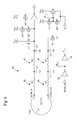
- an RFID transponder 100 of passive type with a security sensor, such as a tamper loop 101 The transponder comprises at least one antenna 110 in order to be able to communicate with an RFID reader 200 via an antenna 210 .
- the RFID transponder 100 comprises separate terminals for connecting the tamper loop 101 .
- the transponder 100 also comprises a radiofrequency signal reception and transmission unit 102 linked to the antenna 110 and supplying power to a power supply circuit 105 .
- a logic unit 103 is provided with a memory in which an identification code to be transmitted is stored, and which is linked to a circuit 104 for detecting the state of the tamper loop.
- the transponder 100 comprises a radiofrequency signal receiver 102 and transmitter 109 . It also comprises a non-volatile memory 106 for storing various data, including the state of the tamper loop, and a state detection circuit 107 linked to a unit 108 for managing the loop.
- this tamper loop 101 requires three connection terminals with one terminal linked to the ground terminal, one terminal linked to the management unit 108 and one terminal linked to a current source Ipol by way of a resistor R 1 .
- Another resistor R 2 is arranged between the terminal linked to ground and the one linked to the management unit 108 .
- FIG. 3 shows an overview of the principle of operation of a tamper loop 101 connected to two connection terminals Tamper_in and Tamper_out of the integrated circuit of a transponder.
- a logic input signal Tamper_en controls the use of the unit for managing the state of the tamper loop 101 .
- This input signal Tamper_en makes it possible to control the closure of a first switch S 1 linked between a current source I 1 linked to a supply voltage Vsup and a first connection terminal Tamper_in of the loop.
- the input signal Tamper_en also makes it possible to control the closure of a second switch S 2 between a second connection terminal Tamper_out of the loop and a current source I 2 linked to ground.
- the value of the current from the current source I 1 is greater than the value of the current from the current source I 2 , for example 10 times greater.
- An inverter 120 may also be provided by connection to the second connection terminal Tamper_out for supplying an output signal Short for the state of the tamper loop 101 . When the two switches S 1 and S 2 are closed, the state of the output signal of the inverter 120 is in the low state so as to indicate that the tamper loop is not broken, and in the high state if the loop is broken.
- the transponder generally operates at a low power, which power is limited depending on the electromagnetic field used for the communication. Under these conditions, it must be mandatory for the tamper-evident function of the circuit to consume little current while having a measurement time that is short enough to determine the state of the tamper loop. It must also not be disturbed by a parasitic capacitor of an external assembly connected to the terminals of the tamper loop when the latter is absent or broken.
- the aim of the invention is therefore to mitigate the drawbacks of the abovementioned prior art by providing a dual communication frequency RFID circuit equipped with a tamper loop linked to a management unit.
- the invention relates to a dual communication frequency RFID circuit equipped with a tamper loop linked to a management unit, which RFID circuit comprises a dual communication frequency RFID circuit, comprising a logic unit for processing data signals received or transmitted at a first frequency by a first antenna or at a second frequency by a second antenna, the first communication frequency being lower than the second communication frequency, the logic unit being connected to a unit for managing the state of a tamper loop linked to the integrated circuit by two connection terminals,
- the management unit comprises at least one first low-pass filter linked to a first connection terminal, at least one second low-pass filter linked to a second connection terminal, a current source for supplying a current through the first low-pass filter, a switch linked at the output of the second low-pass filter, and a first inverter connected between the current source and the first low-pass filter for supplying an output signal for the state of the tamper loop to the logic unit.
- One advantage of the RFID circuit equipped with a tamper loop lies in the fact that the unit for managing the state of the tamper loop of the RFID circuit is designed so as not to be disturbed by any communication at the two communication frequencies and while taking into account the resonant circuit formed of the tamper loop and of a parasitic capacitor connected to the connection terminals of the tamper loop.
- the RFID circuit comprises at least one low-pass filter linked to each connection terminal of the tamper loop in such a way as to filter out interferences.
- Each filter is designed to filter out interferences from a communication at at least one first frequency and/or at at least one second frequency different from the first frequency.
- Each low-pass filter may be identical so as to guarantee symmetry in order to reduce a quality factor Q of the resonant circuit formed of the loop and of the parasitic capacitor at the input. As a result, any induced voltage on one connection terminal is automatically compensated by the inverse voltage on the other connection terminal.
- the unit for managing the state of the tamper loop of the RFID circuit comprises at least one first low-pass filter linked to each connection terminal of the tamper loop followed by a second low-pass filter for filtering out all of the interferences.
- Each first low-pass filter and each successive second low-pass filter is designed to filter out interferences from a communication at a first frequency and at a second frequency different from the first frequency.
- the first frequency is a frequency of the order of 13.56 MHz
- the second frequency is a frequency of the order of 915 MHz.
- FIG. 1 already cited, schematically shows a first embodiment of an RFID electronic circuit equipped with a tamper loop from the prior art
- FIG. 2 already cited, schematically shows a second embodiment of an RFID electronic circuit equipped with a tamper loop from the prior art
- FIG. 3 shows a schematic overview of a unit for managing the state of a tamper loop for an RFID circuit from the prior art
- FIG. 4 schematically shows an embodiment of a dual communication frequency RFID circuit equipped with a tamper loop according to the invention
- FIG. 5 shows the various components of a unit for managing the state of the tamper loop for the dual communication frequency RFID circuit according to the invention.
- FIG. 4 shows an embodiment of a dual communication frequency RFID circuit equipped with a tamper loop according to the invention.
- the RFID circuit is preferably a transponder 1 that is designed to be able to communicate with an RFID interrogator, such as an RFID reader.
- a first communication frequency may be lower than a second communication frequency.
- the transponder 1 comprises a first antenna 2 designed to operate at a first frequency, which may be a first high frequency situated between 3 MHz and 30 MHz, preferably of the order of 13.56 MHz for establishing an NFC near-field communication.
- This first antenna 2 may receive or transmit communication signals in accordance with a first communication protocol.
- the first antenna 2 is linked to a first modulator/demodulator 5 for modulating the data to be transmitted or demodulating the data to be received.
- the first modulator/demodulator 5 is connected to a logic unit 7 for processing the received demodulated data or the data to be transmitted.
- the logic unit 7 comprises a first HF control unit 8 and a second UHF control unit 9 .
- the first HF control unit 8 is designed to process data in accordance with the first communication protocol
- the second UHF control unit 9 is designed to process data in accordance with a second communication protocol.
- the transponder 1 also comprises a second antenna 4 designed to operate at a second frequency, which may be an ultra-high frequency UHF situated between 300 MHz and 3 GHz, preferably of the order of 915 MHz for establishing long-distance communication.
- the second antenna 4 may receive or transmit communication signals in accordance with the second communication protocol.
- This second communication protocol may be for example the EPC Class-1 Generation-2 (Gen2) protocol.
- the second antenna 4 is linked to a second modulator/demodulator 6 , which is linked to the logic unit 7 .
- the signals received or transmitted in accordance with this second protocol are thus processed by the second UHF control unit 9 .
- the first HF control unit 8 is connected to a first non-volatile memory 10 (NVM_HF), while the second UHF control unit 9 is connected to a second non-volatile memory 11 (NVM_UHF).
- a memory bus 12 may also be provided for connecting the two non-volatile memories.
- a power source 3 is also provided in the RFID circuit (transponder) for supplying the supply voltage Vsup to the various electronic components of the RFID circuit. This transponder may therefore be of passive type, with the supply of electric power supplied by rectifying radiofrequency signals received by the first antenna 2 or the second antenna 4 , or of active type with a power source specific to the RFID circuit.
- the RFID circuit 1 also comprises a unit 20 for managing the state of a tamper loop 21 .
- the tamper loop 21 is generally connected to two terminals or contact or connection pads of the RFID integrated circuit so as to be linked to the management components of the management unit 20 that is connected to the logic unit 7 .
- the management unit 20 determines the state of the tamper loop 21 , which loop may be intact or broken.
- the state of the loop may be communicated to the first HF control unit 8 or to the second UHF control unit 9 so as to transmit this information in accordance with the first protocol or the second protocol.
- the state of the loop may also be stored in one of the non-volatile memories, for example in the second non-volatile memory 11 (NVM_UHF).
- FIG. 5 shows the various components of the unit 20 for managing the state of the tamper loop 21 for the dual communication frequency RFID circuit.
- the tamper loop 21 is connected to two terminals or connection pads Tamper_in and Tamper_out while being associated with a parasitic capacitor Cp defining a resonant circuit with a quality factor Q.
- a logic input signal Tamper_en is supplied from the logic unit so as to control the use of the management unit 20
- an output signal Short is supplied so as to give the state of the tamper loop 21 .
- An input connector in is also provided in order to establish a small reference current available in the RFID circuit.
- the management unit 20 is connected between the supply voltage Vsup and ground.
- the management unit 20 comprises at least one first low-pass filter 25 , formed of a first resistor R 1 linked to the first connection terminal Tamper_in and of a first capacitor C 1 linked to ground.
- the management unit 20 comprises at least one second low-pass filter 26 , formed of a first resistor R 1 linked to the second connection terminal Tamper_out and of a first capacitor C 1 linked to ground.
- the first low-pass filter 25 linked to the first connection terminal is identical to the second low-pass filter 26 linked to the second connection terminal.
- Another pair of low-pass filters may also be connected after the first low-pass filter 25 and the second low-pass filter 26 .
- a third low-pass filter 27 (R 2 , C 2 ) is linked to the first low-pass filter 25 and a fourth low-pass filter 28 (R 2 , C 2 ) is linked to the second low-pass filter 26 .
- a second resistor R 2 of the third low-pass filter 27 is linked to the connecting node for the first resistor R 1 and the first capacitor C 1 of the first low-pass filter 25 , while a second capacitor C 2 is linked to ground.
- a second resistor R 2 of the fourth low-pass filter 28 is linked to the connecting node for the first resistor R 1 and the first capacitor C 1 of the second low-pass filter 26 , while a second capacitor C 2 is linked to ground.
- the third low-pass filter 27 is preferably identical to the fourth low-pass filter 28 , so as to ensure symmetry of the management unit.
- capacitors C 1 , C 2 of the low-pass filters may also be linked to the supply voltage terminal Vsup rather than to ground.
- the connecting node for the second resistor R 2 and the second capacitor C 2 of the third low-pass filter 27 is linked to a first inverter 22 , which supplies an output signal Short representing the state of the tamper loop for the logic unit.
- the connecting node for the second resistor R 2 and the second capacitor C 2 of the fourth low-pass filter 28 is linked in series to an MOS transistor M 1 , which transistor is preferably a first NMOS transistor, the source of which is linked to ground, and which transistor is controlled on its gate by an activation signal s depending directly on a logic input signal Tamper_en supplied from the logic unit.
- the logic input signal is first of all supplied to a second inverter 23 , followed by a third inverter 24 so as to supply the activation signal s.
- the second inverter 23 supplies an inverse activation signal sb.
- a second MOS transistor M 2 is linked between the supply voltage terminal Vsup and the connecting node for the second resistor R 2 and the second capacitor C 2 of the third low-pass filter.
- This second transistor M 2 is preferably a PMOS transistor controlled on its gate by the activation signal s.
- a third MOS transistor M 3 in series with a fourth MOS transistor M 4 , these being arranged between the supply voltage terminal Vsup and the connecting node for the second resistor R 2 and the second capacitor C 2 of the third low-pass filter 27 .
- These third and fourth MOS transistors M 3 , M 4 are preferably PMOS transistors.
- the gate of the third transistor M 3 is controlled by the inverse activation signal sb, while the gate of the fourth transistor M 4 is controlled by a control signal ctl.
- the assembly of the third transistor M 3 and the fourth transistor M 4 forms a current source when the two transistors are put into the on state, so as to flow through the low-pass filters, the tamper loop 21 if this is intact and the first transistor M 1 put into the on state, which transistor is also a switch.
- a sixth MOS transistor M 6 and a seventh MOS transistor M 7 which transistors are preferably PMOS transistors.
- An eighth MOS transistor M 8 which is preferably a PMOS transistor, is connected in parallel with the sixth and seventh PMOS transistors M 6 , M 7 , while being linked between the supply terminal Vsup and the reference current terminal in.
- the gate of the eighth PMOS transistor M 8 is linked to the connecting node for the sixth and seventh PMOS transistors M 6 , M 7 , which node supplies the control signal ctl.
- the gate of the sixth PMOS transistor M 6 is controlled by the activation signal s
- the gate of the seventh PMOS transistor M 7 is controlled by the inverse activation signal sb.
- This fifth transistor M 5 may be a PMOS transistor linked between the power supply of the first inverter 22 and the supply terminal Vsup.
- the gate of the fifth transistor M 5 is controlled by the control signal ctl.
- This fifth transistor M 5 is generally in the on state when the third and fourth transistors M 3 , M 4 are in the on state. However, it may also be envisaged to leave the first inverter 22 always activated and supplied directly at the supply voltage Vsup.
- the logic input signal Tamper_en is set to 0, this meaning that the first transistor M 1 is OFF and the second transistor M 2 is ON. As a result, all of the capacitors C 1 , C 2 via the tamper loop 21 are pre-charged.
- the logic input signal Tamper_en is set to 1, this leading, on the positive power supply Vsup side, to M 2 being switched OFF and it being replaced with the third and fourth PMOS transistors M 3 , M 4 , which are activated by the inverse activation signal sb and the control signal ctl.
- the tamper loop 21 has to work in a noisy electromagnetic environment, as electromagnetic fields are used to communicate with the RFID circuit that is to say with the transponder. As a result, when the tamper loop 21 is present, it has to behave as a short circuit, and when it is open or broken as an open circuit in spite of its inductive characteristic.
- the tamper loop 21 is currently a part of a resonant circuit, which also includes the parasitic capacitor Cp.
- the loop receives the electromagnetic fields and modifies them in terms of voltage, which voltage is amplified by the quality factor Q of the resonant circuit.
- the management unit 20 is thus designed to reduce the quality factor Q of the resonant circuit. This makes it possible to avoid accumulating unwanted energy.
- the circuitry linked to the connection terminals thus has to be symmetrical so as to reduce this quality factor Q. As a result, any induced voltage on one connection terminal is automatically compensated by the inverse voltage on the other connection terminal, and as a result, ground is not disturbed by any injected charge.
- R 1 represents the combined value of the two first resistors R 1 in series in the first and second low-pass filters
- first and second low-pass filters are ineffective against the disturbance of the channel at 13.56 MHz in use in the transponder.
- the second communication channel in the 13.56 MHz band is far from the resonant frequency of the tamper loop 21 associated with the circuitry of the management unit 20 .
- this calculated voltage is evaluated as being slightly too large to be applied directly to the drains of the MOS transistors such as M 1 , M 2 or M 3 , third and fourth low-pass filters R 2 , C 2 have been added.
- the cutoff frequency F 2 of the third and fourth low-pass filters must be around one decade below the 13.56 MHz communication band. Three decades are generally used.
- the second resistance R 2 must be much larger than the first resistance R 1 , while the first capacitance C 1 must be much larger than the second capacitance C 2 , such that the smallest components are able to be neglected.
- the second resistance R 2 must not be excessively high so as to have a low voltage drop Vd when the loop is present, as there is a holding current Im of 40 nA through this resistor. As a result, Vd must remain at a few tens of mV. In the case where the tamper loop 21 is present, this voltage drop across the resistors R 1 , R 2 must in principle be below a switching threshold value of the first inverter 22 , for example below Vsup/2, so as to have an output signal at 1 at the output of the first inverter 22 .
- the intrinsic time constant of the pre-charging or of the discharging of the first capacitor C 1 must be around 1 to 2 ⁇ s, the pre-charging or discharging times being able to have a duration of 100 ⁇ s at most.
- R 2 >>R 1 (200 kOhms>>120 Ohms) and C 1 >>C 2 (5.4 pF>>0.5 pF)
- the circuitry of the management unit 20 with the low-pass filters 25 , 26 , 27 , 28 makes it possible to remove the inductive effects of nearby electromagnetic fields, such that the tamper loop is able to be considered as a detectable short circuit, when it is present.
- the first capacitor C 1 of the first and second low-pass filters also has the property of assisting in the detection of the breakage or the absence of the tamper loop when only the assembly parasitic capacitor Cp remains, because a sharing of charges takes place, thereby avoiding having an erroneous diagnosis.
- a current mirror is in an OFF state, despite the fact that the current in is still available.
- the output signal Short is set to 0, since an NMOS transistor in the first inverter 22 is not controlled in terms of current.
- the control signal Tamper_en is set to 1, this leading, on the positive power supply Vsup side, to the second transistor M 2 being switched OFF and it being replaced with the pair of the third and fourth transistors M 3 , M 4 .
- the fifth transistor M 5 is also capable of giving rise to 40 nA while the current mirror is active.
- the first transistor M 1 is switched ON, this resulting in the discharging of all of the capacitors on both sides of the tamper loop.
- the input of the first inverter 22 is at a level 0 below a switching threshold value of the first inverter 22 . This indicates the presence of a short circuit between Tamper_in and Tamper_out.
- the logic input signal Tamper_en is set to 0, this meaning that the first transistor M 1 is OFF and the second transistor M 2 is ON.
- the capacitors are pre-charged differently.
- the capacitors C 1 and C 2 on the Tamper_in side are completely pre-charged, while the parasitic capacitor Cp and the capacitors C 1 and C 2 on the Tamper_out side are partially charged, as the equivalent capacitor is Cp in series with a parallel assembly of C 1 and C 2 , given that the tamper loop 21 is absent.
- the logic input signal Tamper_en is set to 1, this resulting in the partial discharging of the capacitors C 1 and C 2 that are on the Tamper_out side.
- This discharging has a slight effect on the Tamper_in side, as the parasitic capacitor Cp is only partially charged, leading to a charge sharing of the charges stored in C 1 and C 2 on the Tamper_in side.
- this effect does not have any detrimental consequences, given that the amount of shared charges is not large enough, with consideration to the permitted value of Cp, to reduce the input voltage of the first inverter 22 below its switching point.
- the pair of the third and fourth transistors M 3 , M 4 is active so as to restore the voltage level.
- the level on Tamper_in is held at 1 as the input of the first inverter 22 .
- the output signal Short thus remains in the off state at 0 , this signifying the absence of a short circuit with the open tamper loop.
- the continuous current consumption is limited to 40 nA, this corresponding to the reference current attacking the current mirror, as once the pair of the third and fourth transistors M 3 , M 4 has restored the voltage level, there is no more current through said current mirror. As the tamper loop is absent, no continuous current flows through the first transistor M 1 .
- this unit 20 for managing the tamper loop 21 is that of continuously managing the state of the tamper loop or of a switch.
- the current consumption is limited to 80 nA when the loop is present or the switch is closed, while the signal Short is set to 1.
- the pair of the third and fourth transistors M 3 , M 4 charges the node Tamper_in, driving the output signal Short to 0.
- the evaluation or the determination of the state of the tamper loop 21 may be carried out automatically at programmed periods of time and upon request from the logic unit. In principle, it may also be envisaged that, following detection of breakage of the tamper loop, this information is automatically stored in one of the non-volatile memories, so as to transmit this information upon request through an HF or UHF communication.
- a plurality of low-pass filters may be connected one after the other starting from each connection terminal of the tamper loop.
- the current source formed using the third and fourth MOS transistors may be linked to ground, while the first transistor, as switch, may be linked to the supply voltage.
Landscapes
- Engineering & Computer Science (AREA)
- Physics & Mathematics (AREA)
- General Physics & Mathematics (AREA)
- Computer Hardware Design (AREA)
- Theoretical Computer Science (AREA)
- Microelectronics & Electronic Packaging (AREA)
- Computer Security & Cryptography (AREA)
- Computer Networks & Wireless Communication (AREA)
- General Engineering & Computer Science (AREA)
- Automation & Control Theory (AREA)
- Electromagnetism (AREA)
- Artificial Intelligence (AREA)
- Computer Vision & Pattern Recognition (AREA)
- Signal Processing (AREA)
- Near-Field Transmission Systems (AREA)
- Emergency Alarm Devices (AREA)
- Logic Circuits (AREA)
- Transceivers (AREA)
Abstract
Description
Rc=2·(L/C)1/2,
where Rc is the critical resistance of an LC resonant circuit,
F=1/(2·π·(L·C)1/2,
where F is the resonant frequency of an LC resonant circuit,
Ei=K·L·2·π·F·I,
where Ei is the induced voltage created by a similar loop (L) having a coupling factor K and drawing a current I at the frequency F,
L=μ 0·(π/2)·R,
where R is the radius of the loop and μ0 is the universal constant having a value of 4·π·10−7.
L=μ 0·(π/2)·R=4π·10−7·(π/2)·2·10−2=approximately 40 nH.
C=1/(L·(2·π·F)2)=approximately 2.70 pF.
C1=2·C=2·2.70 pF=5.4 pF.
Rc=2·(L/C)1/2=2·(40 nH/2.70 pF)1/2=approximately 240 Ohms.
R1=Rc/2=120 Ohms.
As a result, the values of the components R1 and C1 of the first and second low-pass filters have been obtained.
Fc=1/(2·π·R1·C1)=246 MHz
Ei=K·L·2·π·F·I=340mV
As this calculated voltage is evaluated as being slightly too large to be applied directly to the drains of the MOS transistors such as M1, M2 or M3, third and fourth low-pass filters R2, C2 have been added.
F2=1/(2·π·R2·C2)=1.59 MHz (approximately three octaves below)
T=R2·2·C1=2.2 μs
Claims (15)
Applications Claiming Priority (3)
| Application Number | Priority Date | Filing Date | Title |
|---|---|---|---|
| EP16206224 | 2016-12-22 | ||
| EP16206224.4A EP3340114B1 (en) | 2016-12-22 | 2016-12-22 | Rfid circuit with two communication frequencies provided with a tamper-proof loop |
| EP16206224.4 | 2016-12-22 |
Publications (2)
| Publication Number | Publication Date |
|---|---|
| US20180182217A1 US20180182217A1 (en) | 2018-06-28 |
| US10152863B2 true US10152863B2 (en) | 2018-12-11 |
Family
ID=57749717
Family Applications (1)
| Application Number | Title | Priority Date | Filing Date |
|---|---|---|---|
| US15/831,444 Active US10152863B2 (en) | 2016-12-22 | 2017-12-05 | Dual communication frequency RFID circuit equipped with a tamper-evident loop |
Country Status (6)
| Country | Link |
|---|---|
| US (1) | US10152863B2 (en) |
| EP (1) | EP3340114B1 (en) |
| JP (1) | JP6611371B2 (en) |
| KR (1) | KR102028261B1 (en) |
| CN (1) | CN108229631B (en) |
| BR (1) | BR102017026801B1 (en) |
Families Citing this family (9)
| Publication number | Priority date | Publication date | Assignee | Title |
|---|---|---|---|---|
| US10725077B2 (en) | 2016-12-01 | 2020-07-28 | Nxp B.V. | Tamper detector |
| EP3364333B1 (en) * | 2017-02-17 | 2022-04-06 | Nxp B.V. | Electronic tamper detection device |
| DE102018002585A1 (en) * | 2018-03-28 | 2019-10-02 | Tönnjes Isi Patent Holding Gmbh | Vehicle identification means |
| WO2019245979A1 (en) * | 2018-06-18 | 2019-12-26 | Avery Dennison Retail Information Services, Llc | Small footprint high performing passive rfid tag |
| CN109858600B (en) * | 2019-03-13 | 2024-07-30 | 高恬溪 | A low-power anti-theft alarm RFID tag |
| EP3734513B1 (en) | 2019-04-30 | 2023-03-08 | EM Microelectronic-Marin SA | A tamper detection device |
| US10789391B1 (en) | 2019-07-22 | 2020-09-29 | Alibaba Group Holding Limited | RFID information processing |
| KR102903289B1 (en) * | 2021-10-22 | 2025-12-23 | 삼성전자 주식회사 | Electronic device and method for testing a cable connect circuit |
| US20260080203A1 (en) * | 2024-09-13 | 2026-03-19 | Trovan Limited | Dual frequency radio-frequency identification device |
Citations (10)
| Publication number | Priority date | Publication date | Assignee | Title |
|---|---|---|---|---|
| EP0825554A1 (en) | 1996-08-13 | 1998-02-25 | Fyrtech Microelectronics AB | Sealing device |
| US6646550B1 (en) * | 2001-08-23 | 2003-11-11 | Battelle Memorial Institute | Radio frequency security system and method for a building facility |
| US6888509B2 (en) * | 2000-03-21 | 2005-05-03 | Mikoh Corporation | Tamper indicating radio frequency identification label |
| US20050242962A1 (en) * | 2004-04-29 | 2005-11-03 | Lind Michael A | Tag device, luggage tag, and method of manufacturing a tag device |
| US20060214789A1 (en) | 2005-03-24 | 2006-09-28 | Joshua Posamentier | Tamper detection with RFID tag |
| US7135973B2 (en) * | 2004-02-13 | 2006-11-14 | Avery Dennison Corporation | Tamper monitoring article, system and method |
| US20070120381A1 (en) * | 2005-11-15 | 2007-05-31 | Jakob Ehrensvard | Electronic tamper evident seal |
| US7388493B2 (en) * | 2004-10-08 | 2008-06-17 | Bartronics America, Inc. | Method and system for preventing unauthorized removal and use of an RFID apparatus |
| US20080198011A1 (en) * | 2007-02-16 | 2008-08-21 | John Anthony Leper | Radio-frequency identification tags for preventing and detecting tampering |
| US20110043339A1 (en) | 2009-08-19 | 2011-02-24 | Intelleflex Corporation | RF device with tamper detection |
Family Cites Families (20)
| Publication number | Priority date | Publication date | Assignee | Title |
|---|---|---|---|---|
| JPS53121878U (en) * | 1977-03-04 | 1978-09-28 | ||
| JPH052078U (en) * | 1991-06-24 | 1993-01-14 | 横河電機株式会社 | Probe disconnection detection circuit |
| JP2001216573A (en) * | 2000-02-04 | 2001-08-10 | Kubota Corp | Anti-theft tag |
| GB2412996B (en) * | 2004-04-08 | 2008-11-12 | Gore & Ass | Tamper respondent covering |
| US7471203B2 (en) * | 2005-04-26 | 2008-12-30 | Rf Code, Inc. | Tamper monitoring system and method |
| WO2008102282A2 (en) * | 2007-02-20 | 2008-08-28 | Nxp B.V. | Semiconductor device with backside tamper protection |
| JP5073379B2 (en) * | 2007-06-27 | 2012-11-14 | 株式会社日立製作所 | Non-contact electronic device |
| FR2938953B1 (en) * | 2008-11-21 | 2011-03-11 | Innova Card | DEVICE FOR PROTECTING AN ELECTRONIC INTEGRATED CIRCUIT BOX FROM PHYSICAL OR CHEMICAL INTRUSIONS. |
| US8174388B2 (en) * | 2008-12-10 | 2012-05-08 | Sensormatic Electronics, LLC | Method and system for deactivation of combination EAS/RFID tags |
| WO2010087764A1 (en) * | 2009-01-29 | 2010-08-05 | Ge Healthcare Bioscience Bioprocess Corp. | A system and method for operating rfid devices on single-use connectors |
| JP5178605B2 (en) * | 2009-03-30 | 2013-04-10 | アズビル株式会社 | State control device |
| US8378710B1 (en) * | 2011-09-20 | 2013-02-19 | Nxp B.V. | Secure device anti-tampering circuit |
| US9319088B2 (en) * | 2013-05-09 | 2016-04-19 | Intel Corporation | Radio communication devices and methods for controlling a radio communication device |
| CN103455831B (en) * | 2013-09-04 | 2016-08-17 | 成都芯昊芯科技有限公司 | A kind of passive electronic label that can identify that physical features changes |
| US9342710B2 (en) * | 2013-11-21 | 2016-05-17 | Nxp B.V. | Electronic tamper detection |
| US9741231B2 (en) * | 2014-03-10 | 2017-08-22 | Nxp B.V. | Tamper/damage detection |
| CN105718985B (en) * | 2014-12-04 | 2019-04-30 | 四川凯路威电子有限公司 | RFID anti-counterfeiting circuit |
| US9697711B2 (en) * | 2015-03-19 | 2017-07-04 | The Boeing Company | System and method for tamper detection using RFID devices |
| EP3076341B1 (en) * | 2015-04-02 | 2018-01-10 | EM Microelectronic-Marin SA | Dual frequency hf-uhf identification device, in particular of the passive type |
| EP3076339A1 (en) * | 2015-04-02 | 2016-10-05 | EM Microelectronic-Marin SA | Multi-frequency transponder |
-
2016
- 2016-12-22 EP EP16206224.4A patent/EP3340114B1/en active Active
-
2017
- 2017-12-05 US US15/831,444 patent/US10152863B2/en active Active
- 2017-12-12 BR BR102017026801-2A patent/BR102017026801B1/en active IP Right Grant
- 2017-12-13 JP JP2017238314A patent/JP6611371B2/en active Active
- 2017-12-21 KR KR1020170177254A patent/KR102028261B1/en active Active
- 2017-12-21 CN CN201711390174.3A patent/CN108229631B/en active Active
Patent Citations (12)
| Publication number | Priority date | Publication date | Assignee | Title |
|---|---|---|---|---|
| EP0825554A1 (en) | 1996-08-13 | 1998-02-25 | Fyrtech Microelectronics AB | Sealing device |
| US6888509B2 (en) * | 2000-03-21 | 2005-05-03 | Mikoh Corporation | Tamper indicating radio frequency identification label |
| US6646550B1 (en) * | 2001-08-23 | 2003-11-11 | Battelle Memorial Institute | Radio frequency security system and method for a building facility |
| US7135973B2 (en) * | 2004-02-13 | 2006-11-14 | Avery Dennison Corporation | Tamper monitoring article, system and method |
| US20050242962A1 (en) * | 2004-04-29 | 2005-11-03 | Lind Michael A | Tag device, luggage tag, and method of manufacturing a tag device |
| US7388493B2 (en) * | 2004-10-08 | 2008-06-17 | Bartronics America, Inc. | Method and system for preventing unauthorized removal and use of an RFID apparatus |
| US20060214789A1 (en) | 2005-03-24 | 2006-09-28 | Joshua Posamentier | Tamper detection with RFID tag |
| WO2006102678A1 (en) | 2005-03-24 | 2006-09-28 | Intel Corporation | Tamper detection with rfid tag |
| US20070120381A1 (en) * | 2005-11-15 | 2007-05-31 | Jakob Ehrensvard | Electronic tamper evident seal |
| US20080198011A1 (en) * | 2007-02-16 | 2008-08-21 | John Anthony Leper | Radio-frequency identification tags for preventing and detecting tampering |
| US20110043339A1 (en) | 2009-08-19 | 2011-02-24 | Intelleflex Corporation | RF device with tamper detection |
| US9082057B2 (en) * | 2009-08-19 | 2015-07-14 | Intelleflex Corporation | RF device with tamper detection |
Non-Patent Citations (1)
| Title |
|---|
| European Search Report dated Jul. 17, 2017 in European Application 16206224.4, filed on Dec. 22, 2016 (with English Translation of Categories of cited documents). |
Also Published As
| Publication number | Publication date |
|---|---|
| BR102017026801A2 (en) | 2018-07-31 |
| KR20180073498A (en) | 2018-07-02 |
| JP2018106708A (en) | 2018-07-05 |
| BR102017026801A8 (en) | 2023-04-11 |
| US20180182217A1 (en) | 2018-06-28 |
| BR102017026801B1 (en) | 2024-01-02 |
| EP3340114A1 (en) | 2018-06-27 |
| EP3340114B1 (en) | 2020-09-30 |
| CN108229631B (en) | 2020-10-27 |
| KR102028261B1 (en) | 2019-10-02 |
| JP6611371B2 (en) | 2019-11-27 |
| CN108229631A (en) | 2018-06-29 |
Similar Documents
| Publication | Publication Date | Title |
|---|---|---|
| US10152863B2 (en) | Dual communication frequency RFID circuit equipped with a tamper-evident loop | |
| CN101366049B (en) | Radio Frequency Identification Device System | |
| US9305193B2 (en) | Contactless communication device and user device including the same | |
| EP1801741B1 (en) | Portable data carrier with active noncontact interface | |
| CN107453787B (en) | Near field communication device including two NFC areas | |
| EP3279837B1 (en) | Electronic tamper detection device | |
| US10419058B2 (en) | Method for controlling the tuning to a communications frequency of an antenna connected to a component designed for contactless communication and corresponding system | |
| US20090247079A1 (en) | Terminal of radio-frequency transmission/reception by inductive coupling | |
| JP2000228637A (en) | Capacitive modulation of electromagnetic transponder | |
| JP3607585B2 (en) | Non-contact response device | |
| US20200287598A1 (en) | Nfc interface with energy management function | |
| KR20170070103A (en) | Power load management | |
| US6799015B1 (en) | Electromagnetic transponder with a frequency detuning | |
| US8120419B2 (en) | Apparatus for type-A demodulation and integrated circuit card including the same | |
| EP4095754B1 (en) | Rfid tag limiter | |
| US20090066482A1 (en) | Radio frequency identification system capable of reducing power consumption and method for operating the same | |
| JP2009118071A (en) | Communication device and communication method | |
| JP4879264B2 (en) | Method and apparatus for security for contactless electronic devices | |
| US10984301B2 (en) | Method for limiting the level of a modulated signal received by a tag and corresponding limiter | |
| JPWO2015037422A1 (en) | Wireless communication device and portable device | |
| US6314143B1 (en) | Circuit configuration for manipulation-protected reception of an OOK-modulated signal | |
| KR102710975B1 (en) | Rf reader capable of detecting rf signal transmitted from rf active device in standby mode | |
| CN222509300U (en) | Circuit structure of sensor, intelligent sensor and safety door switch | |
| Pérez-Nicoli et al. | Back Telemetry | |
| CN117792440A (en) | Sensor, safety door switch and control method thereof |
Legal Events
| Date | Code | Title | Description |
|---|---|---|---|
| AS | Assignment |
Owner name: EM MICROELECTRONIC-MARIN S.A., SWITZERLAND Free format text: ASSIGNMENT OF ASSIGNORS INTEREST;ASSIGNORS:LAMOTHE, CHRISTIAN;MULLER, PAUL;STOJANOVIC, GORAN;REEL/FRAME:044293/0662 Effective date: 20171110 |
|
| FEPP | Fee payment procedure |
Free format text: ENTITY STATUS SET TO UNDISCOUNTED (ORIGINAL EVENT CODE: BIG.); ENTITY STATUS OF PATENT OWNER: LARGE ENTITY |
|
| STCF | Information on status: patent grant |
Free format text: PATENTED CASE |
|
| MAFP | Maintenance fee payment |
Free format text: PAYMENT OF MAINTENANCE FEE, 4TH YEAR, LARGE ENTITY (ORIGINAL EVENT CODE: M1551); ENTITY STATUS OF PATENT OWNER: LARGE ENTITY Year of fee payment: 4 |