US10152257B2 - Random number generation in ferroelectric random access memory (FRAM) - Google Patents
Random number generation in ferroelectric random access memory (FRAM) Download PDFInfo
- Publication number
- US10152257B2 US10152257B2 US15/852,618 US201715852618A US10152257B2 US 10152257 B2 US10152257 B2 US 10152257B2 US 201715852618 A US201715852618 A US 201715852618A US 10152257 B2 US10152257 B2 US 10152257B2
- Authority
- US
- United States
- Prior art keywords
- cells
- cell
- logic value
- data pattern
- sub
- Prior art date
- Legal status (The legal status is an assumption and is not a legal conclusion. Google has not performed a legal analysis and makes no representation as to the accuracy of the status listed.)
- Active
Links
Images


Classifications
-
- G—PHYSICS
- G06—COMPUTING OR CALCULATING; COUNTING
- G06F—ELECTRIC DIGITAL DATA PROCESSING
- G06F3/00—Input arrangements for transferring data to be processed into a form capable of being handled by the computer; Output arrangements for transferring data from processing unit to output unit, e.g. interface arrangements
- G06F3/06—Digital input from, or digital output to, record carriers, e.g. RAID, emulated record carriers or networked record carriers
- G06F3/0601—Interfaces specially adapted for storage systems
- G06F3/0602—Interfaces specially adapted for storage systems specifically adapted to achieve a particular effect
- G06F3/062—Securing storage systems
- G06F3/0623—Securing storage systems in relation to content
-
- G—PHYSICS
- G06—COMPUTING OR CALCULATING; COUNTING
- G06F—ELECTRIC DIGITAL DATA PROCESSING
- G06F7/00—Methods or arrangements for processing data by operating upon the order or content of the data handled
- G06F7/58—Random or pseudo-random number generators
- G06F7/588—Random number generators, i.e. based on natural stochastic processes
-
- G—PHYSICS
- G06—COMPUTING OR CALCULATING; COUNTING
- G06F—ELECTRIC DIGITAL DATA PROCESSING
- G06F3/00—Input arrangements for transferring data to be processed into a form capable of being handled by the computer; Output arrangements for transferring data from processing unit to output unit, e.g. interface arrangements
- G06F3/06—Digital input from, or digital output to, record carriers, e.g. RAID, emulated record carriers or networked record carriers
- G06F3/0601—Interfaces specially adapted for storage systems
- G06F3/0628—Interfaces specially adapted for storage systems making use of a particular technique
- G06F3/0638—Organizing or formatting or addressing of data
-
- G—PHYSICS
- G06—COMPUTING OR CALCULATING; COUNTING
- G06F—ELECTRIC DIGITAL DATA PROCESSING
- G06F3/00—Input arrangements for transferring data to be processed into a form capable of being handled by the computer; Output arrangements for transferring data from processing unit to output unit, e.g. interface arrangements
- G06F3/06—Digital input from, or digital output to, record carriers, e.g. RAID, emulated record carriers or networked record carriers
- G06F3/0601—Interfaces specially adapted for storage systems
- G06F3/0668—Interfaces specially adapted for storage systems adopting a particular infrastructure
- G06F3/0671—In-line storage system
- G06F3/0673—Single storage device
- G06F3/0679—Non-volatile semiconductor memory device, e.g. flash memory, one time programmable memory [OTP]
-
- G—PHYSICS
- G11—INFORMATION STORAGE
- G11C—STATIC STORES
- G11C11/00—Digital stores characterised by the use of particular electric or magnetic storage elements; Storage elements therefor
- G11C11/21—Digital stores characterised by the use of particular electric or magnetic storage elements; Storage elements therefor using electric elements
- G11C11/22—Digital stores characterised by the use of particular electric or magnetic storage elements; Storage elements therefor using electric elements using ferroelectric elements
- G11C11/221—Digital stores characterised by the use of particular electric or magnetic storage elements; Storage elements therefor using electric elements using ferroelectric elements using ferroelectric capacitors
-
- G—PHYSICS
- G11—INFORMATION STORAGE
- G11C—STATIC STORES
- G11C11/00—Digital stores characterised by the use of particular electric or magnetic storage elements; Storage elements therefor
- G11C11/21—Digital stores characterised by the use of particular electric or magnetic storage elements; Storage elements therefor using electric elements
- G11C11/22—Digital stores characterised by the use of particular electric or magnetic storage elements; Storage elements therefor using electric elements using ferroelectric elements
- G11C11/225—Auxiliary circuits
- G11C11/2273—Reading or sensing circuits or methods
-
- G—PHYSICS
- G11—INFORMATION STORAGE
- G11C—STATIC STORES
- G11C11/00—Digital stores characterised by the use of particular electric or magnetic storage elements; Storage elements therefor
- G11C11/21—Digital stores characterised by the use of particular electric or magnetic storage elements; Storage elements therefor using electric elements
- G11C11/22—Digital stores characterised by the use of particular electric or magnetic storage elements; Storage elements therefor using electric elements using ferroelectric elements
- G11C11/225—Auxiliary circuits
- G11C11/2275—Writing or programming circuits or methods
Definitions
- the 2T-2C ferroelectric memory cells 12 1 - 12 n may represent a contiguous set of memory cells, for example, a set of memory cells arranged consecutively on the same word line (cell 12 1 is directly adjacent to cell 12 2 , cell 12 2 is directly adjacent to cell 12 3 , and so forth). In some cases, consecutive cells on multiple word lines may be used together. For example, in a case where each available row in the reversed area includes 128 2T-2C ferroelectric memory cells and a 256-bit random number is generated, process 30 may be performed using two rows of memory cells.
Landscapes
- Engineering & Computer Science (AREA)
- Theoretical Computer Science (AREA)
- Physics & Mathematics (AREA)
- General Physics & Mathematics (AREA)
- Computer Hardware Design (AREA)
- General Engineering & Computer Science (AREA)
- Human Computer Interaction (AREA)
- Pure & Applied Mathematics (AREA)
- Mathematical Optimization (AREA)
- Mathematical Analysis (AREA)
- Computational Mathematics (AREA)
- Power Engineering (AREA)
- Semiconductor Memories (AREA)
Abstract
Disclosed embodiments relate to generating random numbers using two transistor, two capacitor (2T-2C) ferroelectric memory cells. In accordance with one disclosed embodiment, an n-bit random number can be generated by writing to a uniform data pattern to a set of n 2T-2C ferroelectric memory cells in a 1T-1C mode so that all ferroelectric capacitors of the n 2T-2C cells have a polarization state corresponding to the same data value (e.g., all 0's or all 1's). The n 2T-2C cells are then read in a 2T-2C mode, so that a random bit (a 0 or 1) is produced for each cell, resulting in an n-bit random number. The n-bit random number is stored in the n 2T-2C ferroelectric memory cells by a rewrite operation. Such random numbers are useful for many purposes, including security, such as authentication, integrity checking, and encryption, and for identification.
Description
This application is a continuation of and claims the benefit of U.S. patent application Ser. No. 15/467,222 filed on Mar. 23, 2017, which claims the benefit of U.S. Provisional Application Ser. No. 62/313,034, filed Mar. 24, 2016 and entitled “GENERATION OF A RANDOM NUMBER USING FERROELECTRIC MEMORY,” the disclosures of which are incorporated by reference herein in their entireties.
This section is intended to introduce the reader to various aspects of art that may be related to various aspects of the subject matter described and/or claimed below, and is believed to be helpful in providing background information to facilitate a better understanding of the present disclosure. It should be understood that these statements are to be read in this light, not as admissions of prior art.
The present disclosure relates generally to ferroelectric non-volatile memory cells and their use in the context of an electronic device and, more specifically, to generation of random numbers using ferroelectric non-volatile memory cells.
Electronic devices, such as consumer electronics, integrated circuits, embedded systems, microcontrollers, and the like, can often include one or more memory devices that store information, such as data and program instructions. To prevent unauthorized access to such information, such devices may include one or more security measures to protect information. This is particularly useful in cases where the protected information is of a sensitive nature, such as, for example, a patient's medical information stored on a medical device, a user's payment information stored on a “smart” credit card, or even a user's personal information (e.g., internet browsing history, GPS location, text messages) stored on a smartphone. Moreover, there has been a growing trend in recent years to incorporate network connectivity into electronic devices. For instance, some electronic devices that traditionally lacked such network connectivity, such as home appliances, televisions, and even automobiles, are now being manufactured with network connectivity functions. It is envisioned that this trend, sometimes called the “internet of things” (IoT), will continue and that network connectivity will continue to be incorporated into more and more electronic devices. However, network connectivity also presents an additional vector by which an unauthorized user may attempt to access protected information. Accordingly, the need for security measures in electronic devices for protection of information is now more important than ever.
Examples of types of security measures that can be implemented on such electronic devices include authentication measures, integrity monitoring, and encryption. Authentication generally requires that proper credentials, such as a password or key phrase, be supplied in order to access protected information. Integrity checking can be used to monitor for changes in software files to ensure that program software, such as an operating system or application software, has not been modified in an unauthorized manner. Encryption can be used to encode protected information on the device so that only authorized parties have access, usually through the use of one or more digital encryption keys. For example, such digital encryption keys may be based on a symmetric-key algorithm (e.g., Advanced Encryption Standard (AES) 128, 192, or 256 bits) or an asymmetric key algorithm (e.g., using a public/private key pair).
Random number generation is often used to implement the aforementioned security measures. For instance, random numbers can be used to generate passwords for authentication purposes and are often the basis of many encryption schemes. By way of example, random numbers can be used as a basis for generating digital keys, such as for data encryption or file integrity checking (e.g., generating a checksum value). Many current techniques for generating random numbers typically involve software routines and algorithms that generate a pseudo-random number based on an initial seed value. Numbers generated by such a process are pseudo-random because while they might satisfy one or more statistical tests for randomness, they are still determined in part by the initial seed value. It is generally desirable that a random number be as unpredictable as possible. Stated another way, if random numbers used for security purposes can be guessed with any accuracy, the security of any scheme relying on such random numbers is compromised. Accordingly, improved methods of generating random numbers are particularly useful, especially as the need for protecting digital information continues to grow.
A summary of certain embodiments disclosed herein is set forth below. It should be understood that these aspects are presented merely to provide the reader with a brief summary of these certain embodiments and that these aspects are not intended to limit the scope of this disclosure. Indeed, this disclosure may encompass a variety of aspects that may not be set forth below.
Aspects of the present disclosure relate to the generation of random numbers using 2T-2C ferroelectric memory cells. To generate, for example, an n-bit random number, a set of n 2T-2C ferroelectric memory cells are written to in a 1T-1C mode so that all the capacitors in the set of n 2T-2C cells have a polarization state corresponding to the same data value (e.g., all logical 0's or all logical 1's). Each of then 2T-2C cells is then read in a 2T-2C mode, so that a random bit (0 or 1) is produced for each cell, thus producing an n-bit random number. This generated n-bit random number is then stored in the n 2T-2C cells as part of a rewrite process, which is typical of ferroelectric memories due to the destructive nature of their read operations. Such random numbers are useful for many purposes, including security, such as authentication, integrity checking, and encryption, and for identification.
Random numbers generated using 2T-2C ferroelectric memory cells, as described herein, may offer an improved degree of randomness compared to some software-based random number generator algorithms that rely on an initial seed value.
Various features discussed below in relation to one or more of the illustrated embodiments may be incorporated into any of the above-described aspects of the present disclosure alone or in any combination. The brief summary presented above is intended only to familiarize the reader with certain aspects and contexts of embodiments of the present disclosure without limitation to the claimed subject matter.
Various aspects of this disclosure may be better understood upon reading the following detailed description and upon reference to the drawings in which:
One or more specific embodiments of the present disclosure are described below. These embodiments are only examples of the presently disclosed techniques. In an effort to provide a concise description of these embodiments, all features of an actual implementation may not be described in the specification. It should be appreciated that in the development of any such implementation, as in any engineering or design project, numerous implementation-specific decisions are made to achieve the developers' specific goals, such as compliance with system-related and/or business-related constraints, which may vary from one implementation to another. Moreover, it should be appreciated that such development efforts might be complex and time consuming, but would nevertheless be a routine undertaking of design, fabrication, and manufacture for those of ordinary skill having the benefit of this disclosure.
When introducing elements of various embodiments of the present disclosure, the articles “a,” “an,” and “the” are intended to mean that there are one or more of the elements. The terms “comprising,” “including,” and “having” are intended to be inclusive and mean that there may be additional elements other than those listed. The embodiments discussed below are intended to be illustrative examples and should not be construed to mean that they are necessarily preferential in nature. Additionally, it should be understood that references to “one embodiment” or “an embodiment” within the present disclosure are not to be interpreted as excluding the existence of additional embodiments that also incorporate the recited features.
The present disclosure relates to techniques for using ferroelectric random access memory (FRAM) to generate random numbers. As is known in the art, FRAM is a type of non-volatile storage in which the construction of its memory cells are based on capacitors in which the dielectric material is a polarizable ferroelectric material, such as lead zirconate titanate (PZT) or strontium-bismuth-tantalate (SBT), rather than silicon dioxide or silicon nitride as typically used in non-ferroelectric capacitors. Hysteresis in the charge-vs.-voltage (Q-V) characteristic, based on the polarization state of the ferroelectric material, enables the non-volatile storage of binary states in these capacitors. In contrast, conventional MOS capacitors lose their stored charge on power-down of the device. It has been observed that ferroelectric capacitors can be constructed by processes that are largely compatible with modern CMOS integrated circuits, for example by placing the capacitors above the transistor level, between overlying levels of metal conductors.
An important characteristic of ferroelectric capacitors, for purposes of non-volatile storage, is the difference in capacitance exhibited by a ferroelectric capacitor between its polarized states. As fundamental in the art, the capacitance of an element refers to the ratio of stored charge to applied voltage. While a ferroelectric capacitor has a linear capacitance by virtue of its construction as parallel plates separated by a dielectric film (i.e., the ferroelectric material), it also exhibits significant polarization capacitance (i.e., charge storage) in response to changes in polarization state that occurs upon application of a polarizing voltage. For example, referring to FIG. 1 , the polarization of a ferroelectric capacitor from its “−1” state to its “+1” state is reflected in a relatively high capacitance C(−1), reflecting the storage of polarization charge in the capacitor in response to the change of polarization state by the voltage exceeding coercive voltage Vα. On the other hand, a capacitor that already in its “+1” state exhibits little capacitance C(+1) due to polarization, since its ferroelectric domains are already aligned in the direction of the applied coercive voltage, causing little additional polarization charge to be stored. A stored logic state is read by interrogating the capacitance of the ferroelectric capacitors to discern its polarization state.
FRAM memory technology is now commonly used to realize non-volatile solid-state read/write random access memories in many electronic devices, particularly in portable electronic devices and systems for a number of different applications. For example, FRAM memory is considered an attractive component for implantable medical devices, such as pacemakers, defibrillators, and monitoring devices, due to the low power consumption of FRAM memory.
Different types of FRAM memory cell architectures are known, such as one-transistor, one-capacitor (1T-1C) and two-transistor, two-capacitor (2T-2C) architectures. 1T-1C cells are similar to conventional dynamic RAM memory cells and are attractive because of their smaller chip area relative to 2T-2C cells. FIG. 2A illustrates a typical arrangement of a conventional 1T-1C FRAM cell 2 jk, which represents a single cell residing in a row j and a column k of an array of similar cells 2. Cell 2 jk includes ferroelectric capacitor 4 and MOS (metal-oxide semiconductor) n-channel pass transistor 6. The source-drain path of transistor 6 is connected between bit line BLk for column k of the array, and the top plate of ferroelectric capacitor 4; the gate of transistor 6 is controlled by word line WLj for row j of the array. The bottom plate of ferroelectric capacitor 4 is connected to plate line PL for the row, or which may be in common for all cells 2 in the array or array portion, depending on the architecture. As such, 1T-1C FRAM cells are similar in construction to conventional dynamic RAM memory cells. Sense amplifier 8 k is coupled to bit line BLk, and operates to compare the bit line voltage developed by read current iR to a reference voltage VREF generated by a reference voltage generator, or at a “dummy” bit line as may be produced by a reference capacitor, as is known in the art. This reference voltage VREF is typically at an intermediate level between the expected voltages for the “0” and “1” data states.
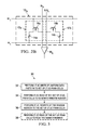
A 2T-2C memory cell includes two ferroelectric capacitors that are polarized to complementary states. FIG. 2B schematically illustrates memory cell 12 j,k of conventional 2T-2C construction. In this example, cell 12 j,k resides in a row j and a column k of a memory array, and includes two ferroelectric capacitors 14 a, 14 b and two MOS transistors 16 a, 16 b. Ferroelectric capacitors 14 a, 14 b are parallel-plate capacitors with ferroelectric material, such as PZT, as the dielectric; one or both of the plates may be formed in a metal or conductive metal compound material (e.g., a silicide, or conductive nitride). For example, the ferroelectric material may be formed over a bottom electrode and covered, for example, by a conductive multi-layer top electrode. One plate of each of ferroelectric capacitors 14 a, 14 b is connected to plate line PLj for row j. The other plate of ferroelectric capacitor 14 a is connected to bit line BLk (the “true” bit line) for column k via the source-drain path of n-channel transistor 16 a. Similarly, the second plate of ferroelectric capacitor 14 b is connected to bit line BLBk (the “complement” bit line) via the source-drain path of n-channel transistor 16 b. The gates of transistors 16 a, 16 b are driven by word line WLj for row j of the memory array.
In operation, ferroelectric capacitors 14 a, 14 b store complementary polarization states that are reflected as a differential voltage or current between bit lines BLk, BLBk when read. As such, a 2T-2C write operation to memory cell 2 j,k consists of applying complementary levels to bit lines BLk, BLBk at a polarity corresponding to the desired data state, while word line WLj is driven active high to turn on transistors 16 a, 16 b; a pulse at plate line PLj during this state causes opposite polarization voltages to polarize capacitors 14 a, 14 b into the corresponding complementary polarization states. In a read operation, bit lines BLk, BLBk are precharged to a selected voltage and then float, after which word line WLj is asserted active high. A pulse at plate line PLj causes the complementary polarization states of capacitors 14 a, 14 b to be reflected as a differential signal across bit lines BLk, BLBk, respectively, for sensing and amplification by sense amplifier 18 k for column k.
In comparing the 1T-1C and 2T-2C FRAM memory cell architectures, the 1T-1C cell has the advantage of increased bit density but the disadvantage of reduced read margin because of its single-ended sense relative to a reference voltage, while the 2T-2C cell provides the advantage of robust data retention from complementary data storage and differential sensing, but at only about one-half the bit density. As can be seen, the 2T-2C cell 12 jk of FIG. 2B is essentially the components of two 1T-1C cells coupled to a common sense amplifier 18 k, but due to the nature of the 2T-2C architecture, when the cell 12 jk is read from or written to in the manner described above, referred to as 2T-2C mode, the cell 12 jk represents one data bit. Stated another way, reading the contents of cell 12 in 2T-2C mode returns one bit of data while writing to cell 12 in 2T-2C mode stores one bit of data.
As is well known in the art, regardless of the cell architecture used to implement a ferroelectric memory cell, ferroelectric memory cells have the characteristic of a destructive read. That is, the act of reading the ferroelectric memory cell results in the stored data being lost. Thus, a read operation on a ferroelectric memory cell includes a rewrite performed immediately thereafter to restore to the cell the information that was read from it, typically during the same cycle as the read operation.
As discussed above, the present disclosure provides techniques for generating a random number using 2T-2C ferroelectric memory cells. An example embodiment of such a technique is described by FIG. 3 , which is a flow diagram depicting a process 30. Process 30 begins at step 32 at which a 1T-1C write of a uniform data pattern is performed on a set of 2T-2C ferroelectric memory cells. A uniform data pattern is a data pattern that has all the same logical values, for example, all logical 1 or all logical 0.
Referring to FIG. 2B , when writing to a 2T-2C cell 12 using a 1T-1C write mode, instead of capacitors 14 a, 14 b being polarized into complementary states, they are polarized into the same state. For the purposes of this description, each transistor and capacitor pair (14 a, 16 a and 14 b, 16 b) of a 2T-2C ferroelectric memory cell may be referred to as a “sub-cell,” for example sub-cells 17 a, 17 b. Thus, each “sub-cell” of the 2T-2C memory cell 12 stores the same logical value. Stated another way, writing to a 2T-2C ferroelectric memory cell in a 1T-1C mode can be viewed as treating each of the sub-cells of the 2T-2C cell as a separate 1T-1C cell. FIG. 4A depicts the result of performing a 1T-1C write of a uniform data pattern of logical 0's to n 2T-2C cells 12 1-12 n. Here, the capacitors of each sub-cell of each of the 2T-2C cells 12 1-12 n are all polarized to a polarization state corresponding to a logical 0. Of course, a uniform data pattern of logical 1's could also be used. As used herein, a uniform data pattern is understood to mean that for a given set of 2T-2C ferroelectric memory cells on which the 1T-1C write is being performed, the sub-cells of every one of the set of 2T-2C cells are written to store the same logical value. Stated another way, the result of writing a uniform data pattern to a set of 2T-2C ferroelectric memory cells in a 1T-1C mode is that the sub-cells within each 2T-2C cell store the same logical value and that all sub-cells of the set of 2T-2C ferroelectric memory cells store that same logical value.
Following the 1T-1C write of the uniform data pattern at step 32, process 30 continues to step 34 at which the set of 2T-2C cells are read in a 2T-2C mode. As discussed above with reference to FIG. 2B , in a normal 2T-2C read operation, the complementary polarization states of capacitors 14 a, 14 b are reflected as a differential signal across bit lines BLk, BLBk, respectively, and that differential signal is sensed and amplified by sense amplifier 18 k for column k to determine the data state stored by the 2T-2C cell. However, because the sub-cells of each 2T-2C cell 12 1-12 n store the same logical value due to the 1T-1C writing of the uniform data pattern, a differential signal does not develop, as the lack of complementary states being stored in the capacitors 14 a, 14 b of the 2T-2C cell will not produce complementary signals on bit lines BLk, BLBk. This results in sense amplifier 18 k producing a random output value that is either a logical 0 or a logical 1. Stated another way, the random output value is generated as a result of providing non-complementary input signals (by bit lines BLk, BLBk) to a differential sense amplifier that expects complementary input signals in order to determine a voltage differential.
Those having ordinary skill in the art will appreciate that in an ideal sense amplifier, the distribution of logical 0's and logical 1's under these circumstances will be approximately 50 percent (e.g., a 0 value is expected half the time and 1 value is expected the other half of the time). In real world practice, however, the sense amplifier may have some amount of offset resulting, for example, from transistor mismatch due to process variations (e.g., dopant number fluctuations, interface-state density fluctuations, etc.) that can cause this distribution to deviate somewhat from 50 percent. Nonetheless, even under real world conditions, it has been found that performing (step 34) a 2T-2C read operation on a 2T-2C ferroelectric memory cell having sub-cells storing the same logic state (as a result of a 1T-1C write of a uniform data pattern) still results in the sense amplifier producing a logical 0 or a logical 1 with a distribution that does not deviate significantly from 50 percent. For example, in testing, it has been observed that the distributions of logical 1's and logical 0's (or vice versa) in real world operation using the present techniques may be approximately 52-48 percent or 53-47 percent, which still provides a sufficiently high degree of randomness. In some embodiment, the randomness may be enhanced by depolarizing the ferroelectric memory cells through exposure to high temperatures. Such exposure may be performed at certain steps during manufacturing, such as during mold curing, wire bonding, or board assembly steps, in which the ferroelectric memory cells may be exposed to temperatures ranging anywhere from 180 to 260 degrees ° C. or higher.
Thus, the result of the 2T-2C read of ferroelectric memory cells 12 1-12 n produces a binary random number value 40 that is n bits long. As will be appreciated, n can be any suitable number, such as 128 for a 128-bit value, 192 for a 192-bit value, or 256 for a 256-bit value (e.g., lengths commonly used in AES encryption). As stated above, since the reading of a ferroelectric memory cell is destructive, the data read from the cell is written back to the cell as part of the read operation (e.g., in the same memory cycle as the read operation). Accordingly, at step 36 of process 30, the random number 40 generated at step 34 is rewritten into the 2T-2C cells using a 2T-2C write operation (as opposed to the 1T-1C write operation used at step 32). This is illustrated by FIG. 4C , which depicts the rewriting of the n bit random number 40 into the 2T-2C cells 12 1-12 n using a 2T-2C write operation. Assuming, by way of example, that 2T-2C cell 12 1 corresponds to cell 12 jk of FIG. 2B , complementary levels are applied to bit lines BLk, BLBk at a polarity corresponding to the desired data state, while word line WLj is driven active high to turn on transistors 16 a, 16 b. Since the data state read from 2T-2C cell 12 1 is a logical 1, the data state to be rewritten is a logical 1. A pulse at plate line PLj during this state causes opposite polarization voltages to polarize capacitors 14 a, 14 b into the corresponding complementary polarization states in which a logical 1 is stored in capacitor 14 a and the complement, a logical 0, is stored in capacitor 14 b.
Using cell 12 jk of FIG. 2B as a reference for all the other 2T-2C cells 12 2-12 n then, in a similar manner, rewriting of the logical 0 read from 2T-2C cell 12 2 results in storing a logical 0 polarization state in capacitor 14 a and a logical 1 polarization state in capacitor 14 b, rewriting of the logical 0 from 2T-2C cell 12 3 results in storing a logical 0 polarization state in capacitor 14 a and a logical 1 polarization state in capacitor 14 b, rewriting of the logical 1 read from 2T-2C cell 12 4 results in storing a logical 1 polarization state in capacitor 14 a and a logical 0 polarization state in capacitor 14 b, rewriting of the logical 1 read from 2T-2C cell 12 5 results in storing a logical 1 polarization state in capacitor 14 a and a logical 0 polarization state in capacitor 14 b, rewriting of the logical 0 read from 2T-2C cell 12 n-1 results in storing a logical 0 polarization state in capacitor 14 a and a logical 1 polarization state in capacitor 14 b, and rewriting of the logical 1 read from 2T-2C cell 12 n-1 results in storing a logical 1 polarization state in capacitor 14 a and a logical 0 polarization state in capacitor 14 b.
Referring again to FIG. 3 , at the completion of step 36, the generated random number 40 is stored in the same 2T-2C ferroelectric memory cells used to generate it at step 34. Since FRAM is a non-volatile storage, this random number is stored persistently and remains available until overwritten or erased. While steps 32 through 36 describe the generation of a random number, it is understood that once generated, the random number stored in the set of 2T-2C memory cells (e.g., cells 12 1-12 n) can be accessed by performing a 2T-2C read on that set of 2T-2C memory cells. For instance, a 2T-2C read performed on memory cells 12 1-12 n (shown as additional step 38 in FIG. 3 ) after the steps 32 to 36 have been performed will produce random number 40.
Those skilled in the art will appreciate that process 30 can be carried out at various stages during manufacture of the ferroelectric memory cells. As one example, process 30 can be performed by the manufacturer during wafer probe testing on a ferroelectric memory die containing an array of 2T-2C cells while the die is still part of an uncut wafer. Thus, a random number may be generated and stored in the FRAM array on the die prior to singulation and packaging.
In another example, the 1T-1C write (step 32) of process 30 can be performed by the manufacturer during wafer probe testing, with the 2T-2C read (step 34) and rewrite (step 36) being performed after packaging the ferroelectric memory die. In a further example, the 1T-1C write (step 32) of process 30 is performed by the manufacturer after packaging the ferroelectric memory die, but the 2T-2C read (step 34) and rewrite (step 36) is performed by a customer who purchases the packaged ferroelectric memory device from the manufacturer. In yet another example, the manufacturer does not perform any steps of process 30 and, instead, process 30 is performed by the customer. For example, issuing a specific command to the FRAM device or entering a test mode can allow access to functionality provided by process 30 to generate a random number.
Further, while the above embodiment describes the use of a uniform data pattern in performing the 1T-1C write (step 32), in another embodiment, the data pattern written in 1T-1C mode can be a non-uniform data pattern. As used herein, a non-uniform data pattern is understood to mean that for a given set of 2T-2C ferroelectric memory cells on which the 1T-1C write is being performed, the two sub-cells for a first 2T-2C cell of the set will store the same logical value, and the two sub-cells of a second 2T-2C cell of the set (e.g., an adjacent cell) will store the same logical value but not necessarily the same logical value as the sub-cells of the first 2T-2C cell. Stated another way, the result of writing a non-uniform data pattern to a set of 2T-2C ferroelectric memory cells in a 1T-1C mode is that sub-cells of different 2T-2C cells in the set can store different logical values so long as the sub-cells of the same 2T-2C cell store the same logical value, thus allowing each 2T-2C cell to produce a random bit value that is either a logical 0 or logical 1 when read in the 2T-2C mode (step 34 of FIG. 3 ).
As an example, a non-uniform data pattern can be a pattern of logical 1's and logical 0's that alternates for each 2T-2C cell. For instance, the two sub-cells of a first 2T-2C cell are each written to a value of logical 1, the two sub-cells of a second 2T-2C cell directly adjacent (e.g., on the same word line) to the first 2T-2C cell are each written to a value of logical 0, the two sub-cells of a third 2T-2C cell directly adjacent to the second 2T-2C cell are each written to a value of logical 1, and so forth. As another example, the non-uniform data pattern is not necessarily an alternating pattern, but includes any data pattern where some of the 2T-2C cells of the set have both of their sub-cells written to a logical 1 value while the remainder of the 2T-2C cells of the set have both of their sub-cells written to a logical 0 value. In some embodiments, the non-uniform data pattern may be selected based on hysteretic characteristics of the 2T-2C cells and/or the random number generated may be at least partially dependent on such hysteretic characteristics (e.g., for non-symmetrical hysteresis, a 2T-2C cell may exhibit a tendency to program more easily toward one of the logical values 0 or 1 than the other).
Accordingly, the embodiments described herein provide a robust technique for generating random numbers that do not require the use of pseudo-random number generator software-based algorithms that use an initial seed value. By basing the generation of each bit of the random number 40 on a random behavior of a differential sense amplifier (i.e., generating an output without complementary input signals), the generation of random numbers using such methods may, in some cases, provide a better degree of randomness compared to some known pseudo-random algorithms. As stated above, random numbers generated using the disclosed techniques are useful as security measures for protecting information that may be stored in an FRAM memory, such as for purposes of authentication (e.g., passwords), file integrity checking (e.g., checksum values), and data encryption (e.g., encryption keys). Such random numbers can also be used for other purposes, such as generating a unique identification or serial number for the FRAM memory or a device containing the FRAM memory.
An FRAM device that implements the random number generation techniques described above may be a stand-alone memory device, or may be part (e.g., a component) of an electronic device. Referring now to FIG. 5 , a functional block diagram of an electronic device 50 that includes FRAM 52 implementing such random number generation techniques is illustrated in accordance with an embodiment. Electronic device 50 includes a processor 54, which is connected to a system bus SBUS. FRAM 52, as well as random access memory (RAM) 56, reside on system bus SBUS as memory resources accessible to processor 54.
As stated above, FRAM 52 provides non-volatile storage and can be used for persistent storage of data, whereas RAM 56, such as dynamic random access memory (DRAM), is typically volatile and loses its data state once power is removed. FRAM 52 may serve as program memory storing program instructions executable by the processor 54. Both RAM 56 and FRAM 52 may serve as data memory. In some cases, program instructions may reside in RAM 56 for recall and execution by processor 54. Other system functions are shown, in a generic sense, in device 50 by way of system control logic 58 and input/output interface 60.
The illustrative electronic device 50 of FIG. 5 may be any type of device that incorporates memory and/or non-volatile memory. For example, device 50 may be a microcontroller unit or embedded processing unit. In one such embodiment, device 50 may be a microcontroller unit (MCU) capable of operating over a wide temperature range with generally low power consumption, and which includes a low power processor, a volatile memory, such as SRAM, non-volatile memory, as well as analog and mixed signal and power management circuitries. Such a device may be suitable for a number of applications in various industries, for example, industrial, medical device, and automotive applications. By way of example only, device 50 may be a model of an embedded processor, a microcontroller unit, a SoC, or a digital signal processor available from Texas Instruments Incorporated of Dallas, Tex. In one embodiment, the device 50 may also be a stand-alone ferroelectric memory device based on FRAM 52, in which case processor 54 and other functions shown in FIG. 5 are not necessarily included.
Further, device 50 may include additional or alternative functions to those shown in FIG. 5 , or may have its functions arranged according to a different architecture from that shown. For instance, in other embodiments, device 50 may be a computing device, such as a mobile telephone (including smartphones), digital media player, a desktop, tablet, or notebook computer, a wearable computing device, and so forth. In such embodiments, device 50 may include additional functional blocks not shown in FIG. 1 , such as input structures, various sensors, and a display. The various functions of device 50 may be realized and implemented using hardware elements (e.g., circuitry), software elements (e.g., computer instructions stored on a tangible computer-readable medium) or a combination of both hardware and software elements. Thus, the architecture and functionality of device 50 shown in FIG. 1 are provided by way of example, and are not intended to limit the scope of this disclosure.
In the embodiment shown in FIG. 5 , FRAM 52 may include an array of 2T-2C ferroelectric memory cells, for example, of the type described above in FIG. 2B . A portion of the FRAM array, shown in FIG. 5 as reserved area 66, may be used for generating random numbers using the above-described methods. Reserved area 66 may be configured as a dedicated area of the array for generating and storing random numbers. Thus, applications executing on device 50 may be unable to access reserved area 66 of the FRAM array unless a given application has permission to access and/or generate a random number (e.g., encryption software for generating a digital key). As will be appreciated, restricting access to reserved area 66 can be accomplished using in any suitable manner, for example, restricting access to memory addresses corresponding to cells in reserved area 66. Depending on the size of reserved area 66 (e.g., the number of available cells), multiple random numbers or various lengths may be generated and stored. As will be appreciated, FRAM 52 may include a controller or, in some cases, processor 54 may act as a controller, to control the various functions of FRAM 52.
Referring to the example of generating and storing a random number 40 in FIGS. 4A to 4C , the 2T-2C ferroelectric memory cells 12 1-12 n may represent a contiguous set of memory cells, for example, a set of memory cells arranged consecutively on the same word line (cell 12 1 is directly adjacent to cell 12 2, cell 12 2 is directly adjacent to cell 12 3, and so forth). In some cases, consecutive cells on multiple word lines may be used together. For example, in a case where each available row in the reversed area includes 128 2T-2C ferroelectric memory cells and a 256-bit random number is generated, process 30 may be performed using two rows of memory cells.
In other embodiments, the set of 2T-2C ferroelectric memory cells used to generate the random number 40 may be non-contiguous. For example, as stated above, sense amplifiers used in conjunction with reading data from 2T-2C ferroelectric memory cells may exhibit some degree of offset that can be the result of transistor mismatch due to process variations. In some manufacturing processes, transistors that are closer together (e.g., adjacent transistors) may be subject to similar process variations. Sense amplifier offsets due to such process variations can, to some degree, influence the randomness of the reading step 34 in FIG. 3 . Thus, in one embodiment, the set of ferroelectric memory cells used generate random number 40 may be non-contiguous. For instance, the set of cells may be on the same word line, but may include non-consecutive cells. Referring to FIG. 6 , consider a simplified example in which a 3-bit random number is generated using cells 12 0,0, 12 0,2, and 12 0,3. In this case, cells 12 0,0 and 12 0,2 are on the same word line WL0 but are not consecutively arranged.
In a further embodiment, the set of cells used to generate random number 40 may be distributed across different word lines, and can include consecutive or non-consecutive cells on the word lines. For instance, referring to FIG. 6 still, consider another simplified example in which a 4-bit random number is generated using cells 12 3,0, 12 1,1, 12 1,2, and 12 2,3. In this case, the cells used to generate the random number are spread across word lines WL3, WL1, and WL2. Thus, depending on process variations that might exist with respect to the transistors in an FRAM array, using non-contiguous cells in the array can help to lessen any influence such process variations may have on randomness.
As will be understood, the various techniques described above and relating to the generation of random numbers using ferroelectric random access memory cells are provided herein by way of example only. Accordingly, it should be understood that the present disclosure should not be construed as being limited to only the examples provided above. Aspects of the techniques disclosed herein may be implemented in any suitable manner, including hardware (suitably configured circuitry), software (e.g., via a computer program including executable code stored on one or more tangible computer readable medium), or a combination of both hardware and software elements.
While the specific embodiments described above have been shown by way of example, it will be appreciated that many modifications and other embodiments will come to the mind of one skilled in the art having the benefit of the teachings presented in the foregoing description and the associated drawings. Accordingly, it is understood that various modifications and embodiments are intended to be included within the scope of the appended claims.
Claims (19)
1. A method to generate a random number in memory device, the method comprising:
in a memory array of the memory device in which the memory array includes a set of unit cells, with each unit cell including first and second sub-cells, using a first memory access mode to program a data pattern into the unit cells so that, as a result of programming the data pattern, the first and second sub-cells of any one unit cell of the unit cells store the same logic value; and
after programming the data pattern into the unit cells, using a second memory access mode to read a respective bit value from each of the unit cells, wherein the respective bit value read from each of the unit cells has either a first logic value or a second logic value that is the complement of the first logic value, and wherein the bit values read from the unit cells collectively form bits of the random number.
2. The method of claim 1 , wherein the first logic value is logic 1 and the data pattern is a uniform data pattern of the first logic value such that, after programming the data pattern into the unit cells, all first and second sub-cells store logic 1.
3. The method of claim 1 , wherein the first logic value is logic 1 and the data pattern is a uniform data pattern of the second logic value, such that, after programming the data pattern into the unit cells, all first and second sub-cells store logic 0.
4. The method of claim 1 , wherein each unit cell is coupled to a respective differential sense amplifier and, for each unit cell, using the second memory access mode to read the unit cell comprises:
receiving, at a first input of the respective differential sense amplifier, a first signal from a first bit line coupled to the first sub-cell of the unit cell;
receiving, at a second input of the respective differential sense amplifier, a second signal from a second bit line coupled to the second sub-cell of the unit cell; and
producing, at an output of the respective differential sense amplifier, an output signal based on the first and second signals;
wherein the output signal is the respective bit value read from the unit cell having either the first logic value or the second logic value.
5. The method of claim 4 , wherein:
the unit cells are ferroelectric random access memory (FRAM) cells;
each FRAM cell includes first and second access transistors and first and second ferroelectric capacitors;
the first access transistor and the first ferroelectric capacitor form the first sub-cell; and
the second access transistor and the second ferroelectric capacitor form the second sub-cell.
6. The method of claim 5 , wherein:
the first memory access mode is a one-transistor-one-capacitor (1T-1C) mode; and
the second memory access mode is a two-transistor-two-capacitor (2T-2C) mode.
7. The method of claim 4 , wherein a probability of the respective bit value being the first logic value or the second logic value is due at least in part to the first and second signals not being complementary signals.
8. The method of claim 4 , wherein a probability of the respective bit value being the first logic value or the second logic value is due at least in part to an offset of the respective differential sense amplifier.
9. The method of claim 1 , wherein the data pattern is not uniform and, as a result of programming the data pattern, the first and second sub-cells of a first unit cell of the unit cells both store the first logic value and the first and second sub-cells of a second unit cell of the unit cells both store the second logic value.
10. The method of claim 1 , further comprising, after using the second memory access mode to read from the unit cells the bit values that form the random number, using the second memory access mode to program the random number into the unit cells.
11. The method of claim 1 , further comprising, after using the second memory access mode to read from the unit cells the bit values that form the random number, using the second memory access mode to program the random number into another set of unit cells of the memory array that are separate from the unit cells.
12. A memory device comprising:
a memory array that includes a set of n unit cells, wherein each unit cell includes first and second sub-cells; and
a memory controller configured to:
use a first memory access mode to program a data pattern into the unit cells so that, as a result of programming the data pattern, the first and second sub-cells of any one unit cell of the unit cells store the same logic value; and
after programming the data pattern into the unit cells, use a second memory access mode to read from the n unit cells n bit values, respectively, wherein each of the n bit values has either a first logic value or a second logic value that is the complement of the first logic value, wherein the n bit values form an n-bit random number.
13. The memory device of claim 12 , wherein the first logic value is logic 1 and the data pattern is a uniform data pattern of the first logic value such that, after programming the data pattern into the unit cells, all first and second sub-cells store logic 1.
14. The memory device of claim 12 , wherein the first logic value is logic 1 and the data pattern is a uniform data pattern of the second logic value, such that, after programming the data pattern into the unit cells, all first and second sub-cells store logic 0.
15. The memory device of claim 12 , wherein the data pattern comprises 2n uniform bits.
16. The memory device of claim 12 , further comprising n differential sense amplifiers each coupled to a respective one of the n unit cells, wherein, for each unit cell, using the second memory access mode to read the unit cell comprises:
receiving, at a first input of a respective differential sense amplifier, a first signal from a first bit line coupled to the first sub-cell of the unit cell;
receiving, at a second input of the respective differential sense amplifier, a second signal from a second bit line coupled to the second sub-cell of the unit cell; and
producing, at an output of the respective differential sense amplifier, an output signal based on the first and second signals;
wherein the output signal is the respective bit value read from the unit cell having either the first logic value or the second logic value.
17. The memory device of claim 16 , wherein:
each of the n unit cells are ferroelectric random access memory (FRAM) cells, each including first and second access transistors and first and second ferroelectric capacitors;
the first access transistor and the first ferroelectric capacitor form the first sub-cell;
the second access transistor and the second ferroelectric capacitor form the second sub-cell;
the first memory access mode is a one-transistor-one-capacitor (1T-1C) mode; and
the second memory access mode is a two-transistor-two-capacitor (2T-2C) mode.
18. The memory device of claim 16 , wherein a probability of the respective bit value being the first logic value or the second logic value is due at least in part to an offset of the respective differential sense amplifier.
19. The method of claim 12 , wherein the data pattern is not uniform and, as a result of programming the data pattern into the unit cells, the first and second sub-cells of a first unit cell of the unit cells both store the first logic value and the first and second sub-cells of a second unit cell of the unit cells both store the second logic value.
Priority Applications (1)
| Application Number | Priority Date | Filing Date | Title |
|---|---|---|---|
| US15/852,618 US10152257B2 (en) | 2016-03-24 | 2017-12-22 | Random number generation in ferroelectric random access memory (FRAM) |
Applications Claiming Priority (3)
| Application Number | Priority Date | Filing Date | Title |
|---|---|---|---|
| US201662313034P | 2016-03-24 | 2016-03-24 | |
| US15/467,222 US9851914B2 (en) | 2016-03-24 | 2017-03-23 | Random number generation in ferroelectric random access memory (FRAM) |
| US15/852,618 US10152257B2 (en) | 2016-03-24 | 2017-12-22 | Random number generation in ferroelectric random access memory (FRAM) |
Related Parent Applications (1)
| Application Number | Title | Priority Date | Filing Date |
|---|---|---|---|
| US15/467,222 Continuation US9851914B2 (en) | 2016-03-24 | 2017-03-23 | Random number generation in ferroelectric random access memory (FRAM) |
Publications (2)
| Publication Number | Publication Date |
|---|---|
| US20180188987A1 US20180188987A1 (en) | 2018-07-05 |
| US10152257B2 true US10152257B2 (en) | 2018-12-11 |
Family
ID=59897923
Family Applications (2)
| Application Number | Title | Priority Date | Filing Date |
|---|---|---|---|
| US15/467,222 Active US9851914B2 (en) | 2016-03-24 | 2017-03-23 | Random number generation in ferroelectric random access memory (FRAM) |
| US15/852,618 Active US10152257B2 (en) | 2016-03-24 | 2017-12-22 | Random number generation in ferroelectric random access memory (FRAM) |
Family Applications Before (1)
| Application Number | Title | Priority Date | Filing Date |
|---|---|---|---|
| US15/467,222 Active US9851914B2 (en) | 2016-03-24 | 2017-03-23 | Random number generation in ferroelectric random access memory (FRAM) |
Country Status (1)
| Country | Link |
|---|---|
| US (2) | US9851914B2 (en) |
Cited By (1)
| Publication number | Priority date | Publication date | Assignee | Title |
|---|---|---|---|---|
| US11956376B2 (en) | 2019-12-17 | 2024-04-09 | Samsung Electronics Co., Ltd. | Memory device and memory system having the same |
Families Citing this family (25)
| Publication number | Priority date | Publication date | Assignee | Title |
|---|---|---|---|---|
| US9990181B2 (en) | 2016-08-03 | 2018-06-05 | Micron Technology, Inc. | Apparatuses and methods for random number generation |
| US10019236B2 (en) * | 2016-08-11 | 2018-07-10 | Taiwan Semiconductor Manufacturing Co., Ltd. | SRAM-based true random number generator |
| US10424361B2 (en) * | 2018-02-09 | 2019-09-24 | Texas Instruments Incorporated | Physical unclonable function system and method |
| FR3080927B1 (en) * | 2018-05-03 | 2024-02-02 | Proton World Int Nv | AUTHENTICATION OF AN ELECTRONIC CIRCUIT |
| TWI669714B (en) * | 2018-05-29 | 2019-08-21 | 力旺電子股份有限公司 | Voltage control device and memory system |
| US11416416B2 (en) * | 2019-01-13 | 2022-08-16 | Ememory Technology Inc. | Random code generator with non-volatile memory |
| US11482529B2 (en) | 2019-02-27 | 2022-10-25 | Kepler Computing Inc. | High-density low voltage non-volatile memory with unidirectional plate-line and bit-line and pillar capacitor |
| US10998025B2 (en) | 2019-02-27 | 2021-05-04 | Kepler Computing, Inc. | High-density low voltage non-volatile differential memory bit-cell with shared plate-line |
| JP7480133B2 (en) * | 2019-05-17 | 2024-05-09 | 株式会社半導体エネルギー研究所 | Semiconductor device and electronic device |
| WO2022064303A1 (en) * | 2020-09-22 | 2022-03-31 | 株式会社半導体エネルギー研究所 | Semiconductor device and electronic apparatus |
| US12125513B2 (en) * | 2021-04-22 | 2024-10-22 | Seagate Technology Llc | System on chip (SOC) with processor and integrated ferroelectric memory |
| US11527277B1 (en) * | 2021-06-04 | 2022-12-13 | Kepler Computing Inc. | High-density low voltage ferroelectric memory bit-cell |
| US11729991B1 (en) | 2021-11-01 | 2023-08-15 | Kepler Computing Inc. | Common mode compensation for non-linear polar material based differential memory bit-cell |
| US11482270B1 (en) | 2021-11-17 | 2022-10-25 | Kepler Computing Inc. | Pulsing scheme for a ferroelectric memory bit-cell to minimize read or write disturb effect and refresh logic |
| US12108609B1 (en) | 2022-03-07 | 2024-10-01 | Kepler Computing Inc. | Memory bit-cell with stacked and folded planar capacitors |
| US12324163B1 (en) | 2022-03-15 | 2025-06-03 | Kepler Computing Inc. | Planar capacitors with shared electrode and methods of fabrication |
| US20230395134A1 (en) | 2022-06-03 | 2023-12-07 | Kepler Computing Inc. | Write disturb mitigation for non-linear polar material based multi-capacitor bit-cell |
| US12593456B1 (en) | 2022-06-17 | 2026-03-31 | Kepler Computing Inc. | Method of fabricating transistors and stacked non-planar capacitors for memory and logic applications |
| US12300297B1 (en) | 2022-08-05 | 2025-05-13 | Kepler Computing Inc. | Memory array with buried or backside word-line |
| US12062584B1 (en) | 2022-10-28 | 2024-08-13 | Kepler Computing Inc. | Iterative method of multilayer stack development for device applications |
| US11741428B1 (en) | 2022-12-23 | 2023-08-29 | Kepler Computing Inc. | Iterative monetization of process development of non-linear polar material and devices |
| US12347476B1 (en) | 2022-12-27 | 2025-07-01 | Kepler Computing Inc. | Apparatus and method to improve sensing noise margin in a non-linear polar material based bit-cell |
| US12334127B2 (en) | 2023-01-30 | 2025-06-17 | Kepler Computing Inc. | Non-linear polar material based multi-capacitor high density bit-cell |
| US11765908B1 (en) | 2023-02-10 | 2023-09-19 | Kepler Computing Inc. | Memory device fabrication through wafer bonding |
| US20240274651A1 (en) | 2023-02-10 | 2024-08-15 | Kepler Computing Inc. | Method of forming stacked capacitors through wafer bonding |
Citations (5)
| Publication number | Priority date | Publication date | Assignee | Title |
|---|---|---|---|---|
| US20020196656A1 (en) * | 1999-06-02 | 2002-12-26 | Kabushiki Kaisha Toshiba | Ferroelectric memory and semiconductor memory |
| US20030235066A1 (en) * | 2002-06-21 | 2003-12-25 | Micron Technology, Inc. | Ferroelectric write once read only memory for archival storage |
| US20080175034A1 (en) * | 2006-11-29 | 2008-07-24 | Fujitsu Limited | Ferroelectric memory and operating method of same |
| US20150355886A1 (en) | 2014-06-10 | 2015-12-10 | Texas Instruments Incorporated | Random Number Generation with Ferroelectric Random Access Memory |
| US9401196B1 (en) | 2015-06-11 | 2016-07-26 | Texas Instruments Incorporated | Dual mode ferroelectric random access memory (FRAM) cell apparatus and methods with imprinted read-only (RO) data |
-
2017
- 2017-03-23 US US15/467,222 patent/US9851914B2/en active Active
- 2017-12-22 US US15/852,618 patent/US10152257B2/en active Active
Patent Citations (5)
| Publication number | Priority date | Publication date | Assignee | Title |
|---|---|---|---|---|
| US20020196656A1 (en) * | 1999-06-02 | 2002-12-26 | Kabushiki Kaisha Toshiba | Ferroelectric memory and semiconductor memory |
| US20030235066A1 (en) * | 2002-06-21 | 2003-12-25 | Micron Technology, Inc. | Ferroelectric write once read only memory for archival storage |
| US20080175034A1 (en) * | 2006-11-29 | 2008-07-24 | Fujitsu Limited | Ferroelectric memory and operating method of same |
| US20150355886A1 (en) | 2014-06-10 | 2015-12-10 | Texas Instruments Incorporated | Random Number Generation with Ferroelectric Random Access Memory |
| US9401196B1 (en) | 2015-06-11 | 2016-07-26 | Texas Instruments Incorporated | Dual mode ferroelectric random access memory (FRAM) cell apparatus and methods with imprinted read-only (RO) data |
Cited By (1)
| Publication number | Priority date | Publication date | Assignee | Title |
|---|---|---|---|---|
| US11956376B2 (en) | 2019-12-17 | 2024-04-09 | Samsung Electronics Co., Ltd. | Memory device and memory system having the same |
Also Published As
| Publication number | Publication date |
|---|---|
| US20170277459A1 (en) | 2017-09-28 |
| US20180188987A1 (en) | 2018-07-05 |
| US9851914B2 (en) | 2017-12-26 |
Similar Documents
| Publication | Publication Date | Title |
|---|---|---|
| US10152257B2 (en) | Random number generation in ferroelectric random access memory (FRAM) | |
| US12244741B2 (en) | Physical unclonable function (PUF) security key generation | |
| TWI744852B (en) | Anti-hacking mechanisms for flash memory device | |
| JP6587188B2 (en) | Random number processing apparatus, integrated circuit card, and random number processing method | |
| JP6817888B2 (en) | Non-volatile memory device | |
| JP6508478B2 (en) | Tamper resistant nonvolatile memory device and integrated circuit card | |
| CN103946854B (en) | The intrinsic fingerprint recognition based on reservation being characterized with fuzzy algorithmic approach and dynamic key | |
| JP6769975B2 (en) | Setting a reference voltage for data sensing in a ferroelectric memory | |
| US10545752B2 (en) | Ferroelectric memory expansion for firmware updates | |
| Holcomb et al. | Bitline PUF: building native challenge-response PUF capability into any SRAM | |
| US20180191512A1 (en) | Physically unclonable function generation with direct twin cell activation | |
| US10078494B2 (en) | Secure true random number generation using 1.5-T transistor flash memory | |
| US10541016B2 (en) | Dual mode memory array security apparatus, systems and methods | |
| US10153025B2 (en) | Circuit and method for imprint reduction in FRAM memories | |
| JP2017011678A (en) | Nonvolatile memory device and integrated circuit card that have resistance to protein, authentication method for nonvolatile memory device and individual identification information generating method | |
| TW201734879A (en) | SRAM-based authentication circuit | |
| Vopson et al. | Four-state anti-ferroelectric random access memory | |
| TW202113649A (en) | Physical unclonable function code generation appratus and method thereof | |
| US20100025747A1 (en) | Method for initializing ferroelectric memory device, ferroelectric memory device, and electronic equipment | |
| CN116170160B (en) | Physical unclonable function circuit and application thereof | |
| US20120191902A1 (en) | One-Die Flotox-Based Combo Non-Volatile Memory | |
| US9531535B2 (en) | Secure memories using unique identification elements | |
| Ahr et al. | RAM-based PUFs: Comparing static-and dynamic random access memory | |
| JP3497154B2 (en) | Method of manufacturing ferroelectric memory and ferroelectric memory | |
| US10269441B1 (en) | Systems and methods for threshold voltage modification and detection |
Legal Events
| Date | Code | Title | Description |
|---|---|---|---|
| FEPP | Fee payment procedure |
Free format text: ENTITY STATUS SET TO UNDISCOUNTED (ORIGINAL EVENT CODE: BIG.); ENTITY STATUS OF PATENT OWNER: LARGE ENTITY |
|
| STCF | Information on status: patent grant |
Free format text: PATENTED CASE |
|
| MAFP | Maintenance fee payment |
Free format text: PAYMENT OF MAINTENANCE FEE, 4TH YEAR, LARGE ENTITY (ORIGINAL EVENT CODE: M1551); ENTITY STATUS OF PATENT OWNER: LARGE ENTITY Year of fee payment: 4 |