US10147864B2 - Fe—Ni/Ti metalized skutterudite thermoelectric material and method of manufacturing the same - Google Patents
Fe—Ni/Ti metalized skutterudite thermoelectric material and method of manufacturing the same Download PDFInfo
- Publication number
- US10147864B2 US10147864B2 US15/695,006 US201715695006A US10147864B2 US 10147864 B2 US10147864 B2 US 10147864B2 US 201715695006 A US201715695006 A US 201715695006A US 10147864 B2 US10147864 B2 US 10147864B2
- Authority
- US
- United States
- Prior art keywords
- layer
- thermoelectric material
- skutterudite
- skutterudite thermoelectric
- metalized
- Prior art date
- Legal status (The legal status is an assumption and is not a legal conclusion. Google has not performed a legal analysis and makes no representation as to the accuracy of the status listed.)
- Active
Links
- 239000000463 material Substances 0.000 title claims abstract description 109
- 229910001030 Iron–nickel alloy Inorganic materials 0.000 title claims abstract description 75
- 238000004519 manufacturing process Methods 0.000 title claims abstract description 13
- 238000001465 metallisation Methods 0.000 claims description 40
- 238000000034 method Methods 0.000 claims description 17
- 239000011888 foil Substances 0.000 claims description 11
- 239000000843 powder Substances 0.000 claims description 11
- 239000002184 metal Substances 0.000 claims description 7
- 229910052751 metal Inorganic materials 0.000 claims description 7
- 229910018985 CoSb3 Inorganic materials 0.000 claims description 4
- 229910000765 intermetallic Inorganic materials 0.000 abstract description 25
- 238000010248 power generation Methods 0.000 abstract description 16
- 238000009792 diffusion process Methods 0.000 abstract description 15
- 230000007774 longterm Effects 0.000 abstract description 9
- 230000015572 biosynthetic process Effects 0.000 abstract description 8
- 230000001747 exhibiting effect Effects 0.000 abstract 1
- 238000002149 energy-dispersive X-ray emission spectroscopy Methods 0.000 description 13
- 238000007669 thermal treatment Methods 0.000 description 11
- 229910045601 alloy Inorganic materials 0.000 description 8
- 239000000956 alloy Substances 0.000 description 8
- 238000005259 measurement Methods 0.000 description 8
- 230000004888 barrier function Effects 0.000 description 5
- 238000011160 research Methods 0.000 description 4
- 238000007731 hot pressing Methods 0.000 description 3
- 238000005245 sintering Methods 0.000 description 3
- 238000002490 spark plasma sintering Methods 0.000 description 3
- 239000000654 additive Substances 0.000 description 2
- 230000000996 additive effect Effects 0.000 description 2
- 238000006243 chemical reaction Methods 0.000 description 2
- 238000005336 cracking Methods 0.000 description 2
- 238000005516 engineering process Methods 0.000 description 2
- 239000000203 mixture Substances 0.000 description 2
- 238000007792 addition Methods 0.000 description 1
- 238000004458 analytical method Methods 0.000 description 1
- 230000003466 anti-cipated effect Effects 0.000 description 1
- 238000005137 deposition process Methods 0.000 description 1
- 230000006866 deterioration Effects 0.000 description 1
- 238000003306 harvesting Methods 0.000 description 1
- 238000012986 modification Methods 0.000 description 1
- 230000004048 modification Effects 0.000 description 1
- 230000008929 regeneration Effects 0.000 description 1
- 238000011069 regeneration method Methods 0.000 description 1
- 238000006467 substitution reaction Methods 0.000 description 1
- 239000002918 waste heat Substances 0.000 description 1
Images


Classifications
-
- H01L37/025—
-
- H—ELECTRICITY
- H10—SEMICONDUCTOR DEVICES; ELECTRIC SOLID-STATE DEVICES NOT OTHERWISE PROVIDED FOR
- H10N—ELECTRIC SOLID-STATE DEVICES NOT OTHERWISE PROVIDED FOR
- H10N10/00—Thermoelectric devices comprising a junction of dissimilar materials, i.e. devices exhibiting Seebeck or Peltier effects
- H10N10/80—Constructional details
- H10N10/85—Thermoelectric active materials
- H10N10/851—Thermoelectric active materials comprising inorganic compositions
-
- B—PERFORMING OPERATIONS; TRANSPORTING
- B32—LAYERED PRODUCTS
- B32B—LAYERED PRODUCTS, i.e. PRODUCTS BUILT-UP OF STRATA OF FLAT OR NON-FLAT, e.g. CELLULAR OR HONEYCOMB, FORM
- B32B15/00—Layered products comprising a layer of metal
- B32B15/04—Layered products comprising a layer of metal comprising metal as the main or only constituent of a layer, which is next to another layer of the same or of a different material
- B32B15/043—Layered products comprising a layer of metal comprising metal as the main or only constituent of a layer, which is next to another layer of the same or of a different material of metal
-
- H—ELECTRICITY
- H10—SEMICONDUCTOR DEVICES; ELECTRIC SOLID-STATE DEVICES NOT OTHERWISE PROVIDED FOR
- H10N—ELECTRIC SOLID-STATE DEVICES NOT OTHERWISE PROVIDED FOR
- H10N15/00—Thermoelectric devices without a junction of dissimilar materials; Thermomagnetic devices, e.g. using the Nernst-Ettingshausen effect
- H10N15/10—Thermoelectric devices using thermal change of the dielectric constant, e.g. working above and below the Curie point
- H10N15/15—Thermoelectric active materials
-
- B—PERFORMING OPERATIONS; TRANSPORTING
- B32—LAYERED PRODUCTS
- B32B—LAYERED PRODUCTS, i.e. PRODUCTS BUILT-UP OF STRATA OF FLAT OR NON-FLAT, e.g. CELLULAR OR HONEYCOMB, FORM
- B32B15/00—Layered products comprising a layer of metal
- B32B15/16—Layered products comprising a layer of metal next to a particulate layer
-
- B—PERFORMING OPERATIONS; TRANSPORTING
- B32—LAYERED PRODUCTS
- B32B—LAYERED PRODUCTS, i.e. PRODUCTS BUILT-UP OF STRATA OF FLAT OR NON-FLAT, e.g. CELLULAR OR HONEYCOMB, FORM
- B32B15/00—Layered products comprising a layer of metal
- B32B15/18—Layered products comprising a layer of metal comprising iron or steel
-
- B—PERFORMING OPERATIONS; TRANSPORTING
- B32—LAYERED PRODUCTS
- B32B—LAYERED PRODUCTS, i.e. PRODUCTS BUILT-UP OF STRATA OF FLAT OR NON-FLAT, e.g. CELLULAR OR HONEYCOMB, FORM
- B32B19/00—Layered products comprising a layer of natural mineral fibres or particles, e.g. asbestos, mica
- B32B19/04—Layered products comprising a layer of natural mineral fibres or particles, e.g. asbestos, mica next to another layer of the same or of a different material
- B32B19/041—Layered products comprising a layer of natural mineral fibres or particles, e.g. asbestos, mica next to another layer of the same or of a different material of metal
-
- B—PERFORMING OPERATIONS; TRANSPORTING
- B32—LAYERED PRODUCTS
- B32B—LAYERED PRODUCTS, i.e. PRODUCTS BUILT-UP OF STRATA OF FLAT OR NON-FLAT, e.g. CELLULAR OR HONEYCOMB, FORM
- B32B5/00—Layered products characterised by the non- homogeneity or physical structure, i.e. comprising a fibrous, filamentary, particulate or foam layer; Layered products characterised by having a layer differing constitutionally or physically in different parts
- B32B5/16—Layered products characterised by the non- homogeneity or physical structure, i.e. comprising a fibrous, filamentary, particulate or foam layer; Layered products characterised by having a layer differing constitutionally or physically in different parts characterised by features of a layer formed of particles, e.g. chips, powder or granules
-
- H—ELECTRICITY
- H10—SEMICONDUCTOR DEVICES; ELECTRIC SOLID-STATE DEVICES NOT OTHERWISE PROVIDED FOR
- H10N—ELECTRIC SOLID-STATE DEVICES NOT OTHERWISE PROVIDED FOR
- H10N10/00—Thermoelectric devices comprising a junction of dissimilar materials, i.e. devices exhibiting Seebeck or Peltier effects
- H10N10/01—Manufacture or treatment
-
- H—ELECTRICITY
- H10—SEMICONDUCTOR DEVICES; ELECTRIC SOLID-STATE DEVICES NOT OTHERWISE PROVIDED FOR
- H10N—ELECTRIC SOLID-STATE DEVICES NOT OTHERWISE PROVIDED FOR
- H10N10/00—Thermoelectric devices comprising a junction of dissimilar materials, i.e. devices exhibiting Seebeck or Peltier effects
- H10N10/10—Thermoelectric devices comprising a junction of dissimilar materials, i.e. devices exhibiting Seebeck or Peltier effects operating with only the Peltier or Seebeck effects
- H10N10/17—Thermoelectric devices comprising a junction of dissimilar materials, i.e. devices exhibiting Seebeck or Peltier effects operating with only the Peltier or Seebeck effects characterised by the structure or configuration of the cell or thermocouple forming the device
-
- H—ELECTRICITY
- H10—SEMICONDUCTOR DEVICES; ELECTRIC SOLID-STATE DEVICES NOT OTHERWISE PROVIDED FOR
- H10N—ELECTRIC SOLID-STATE DEVICES NOT OTHERWISE PROVIDED FOR
- H10N10/00—Thermoelectric devices comprising a junction of dissimilar materials, i.e. devices exhibiting Seebeck or Peltier effects
- H10N10/80—Constructional details
- H10N10/85—Thermoelectric active materials
- H10N10/851—Thermoelectric active materials comprising inorganic compositions
- H10N10/854—Thermoelectric active materials comprising inorganic compositions comprising only metals
-
- B—PERFORMING OPERATIONS; TRANSPORTING
- B32—LAYERED PRODUCTS
- B32B—LAYERED PRODUCTS, i.e. PRODUCTS BUILT-UP OF STRATA OF FLAT OR NON-FLAT, e.g. CELLULAR OR HONEYCOMB, FORM
- B32B38/00—Ancillary operations in connection with laminating processes
- B32B2038/0052—Other operations not otherwise provided for
- B32B2038/0092—Metallizing
-
- B—PERFORMING OPERATIONS; TRANSPORTING
- B32—LAYERED PRODUCTS
- B32B—LAYERED PRODUCTS, i.e. PRODUCTS BUILT-UP OF STRATA OF FLAT OR NON-FLAT, e.g. CELLULAR OR HONEYCOMB, FORM
- B32B2250/00—Layers arrangement
- B32B2250/03—3 layers
-
- B—PERFORMING OPERATIONS; TRANSPORTING
- B32—LAYERED PRODUCTS
- B32B—LAYERED PRODUCTS, i.e. PRODUCTS BUILT-UP OF STRATA OF FLAT OR NON-FLAT, e.g. CELLULAR OR HONEYCOMB, FORM
- B32B2262/00—Composition or structural features of fibres which form a fibrous or filamentary layer or are present as additives
- B32B2262/10—Inorganic fibres
-
- B—PERFORMING OPERATIONS; TRANSPORTING
- B32—LAYERED PRODUCTS
- B32B—LAYERED PRODUCTS, i.e. PRODUCTS BUILT-UP OF STRATA OF FLAT OR NON-FLAT, e.g. CELLULAR OR HONEYCOMB, FORM
- B32B2307/00—Properties of the layers or laminate
- B32B2307/20—Properties of the layers or laminate having particular electrical or magnetic properties, e.g. piezoelectric
-
- B—PERFORMING OPERATIONS; TRANSPORTING
- B32—LAYERED PRODUCTS
- B32B—LAYERED PRODUCTS, i.e. PRODUCTS BUILT-UP OF STRATA OF FLAT OR NON-FLAT, e.g. CELLULAR OR HONEYCOMB, FORM
- B32B2307/00—Properties of the layers or laminate
- B32B2307/30—Properties of the layers or laminate having particular thermal properties
-
- B—PERFORMING OPERATIONS; TRANSPORTING
- B32—LAYERED PRODUCTS
- B32B—LAYERED PRODUCTS, i.e. PRODUCTS BUILT-UP OF STRATA OF FLAT OR NON-FLAT, e.g. CELLULAR OR HONEYCOMB, FORM
- B32B2307/00—Properties of the layers or laminate
- B32B2307/70—Other properties
- B32B2307/732—Dimensional properties
-
- B—PERFORMING OPERATIONS; TRANSPORTING
- B32—LAYERED PRODUCTS
- B32B—LAYERED PRODUCTS, i.e. PRODUCTS BUILT-UP OF STRATA OF FLAT OR NON-FLAT, e.g. CELLULAR OR HONEYCOMB, FORM
- B32B2309/00—Parameters for the laminating or treatment process; Apparatus details
- B32B2309/08—Dimensions, e.g. volume
- B32B2309/10—Dimensions, e.g. volume linear, e.g. length, distance, width
- B32B2309/105—Thickness
-
- B—PERFORMING OPERATIONS; TRANSPORTING
- B32—LAYERED PRODUCTS
- B32B—LAYERED PRODUCTS, i.e. PRODUCTS BUILT-UP OF STRATA OF FLAT OR NON-FLAT, e.g. CELLULAR OR HONEYCOMB, FORM
- B32B2457/00—Electrical equipment
Definitions
- thermoelectric material which is able to convert thermal energy into electrical energy
- thermoelectric power generation module so as to realize thermoelectric power generation.
- the thermoelectric power generation technique is an energy-harvesting process for converting thermal energy into electrical energy, and is also receiving attention in the field of renewable energy technology because it may be used in industrial sites and any places where waste heat may be generated.
- the Fe—Ni layer is preferably composed of Fe and Ni at a weight ratio ranging from 75:25 to 55:45.
- the thickness of the Fe—Ni layer is 40 ⁇ m or more, an intermetallic compound layer may be appropriately formed and the Fe—Ni layer may also function as a thermal expansion buffer layer.
- the upper limit of the thickness of the Fe—Ni layer is not particularly limited, but is preferably 150 ⁇ m or less taking into consideration the manufacturing cost.
- the thickness of the Fe—Ni layer is 40 ⁇ m or more, an intermetallic compound layer may be appropriately formed and the Fe—Ni layer may also play a role as a thermal expansion buffer layer.
- the upper limit of the thickness of the Fe—Ni layer is not particularly limited, but is preferably 150 ⁇ m or less taking into consideration the manufacturing cost.
- the present invention provides a method of forming a metalization layer configured such that a Fe—Ni layer is formed on the thermoelectric material and a Ti layer is disposed thereon.
- the Fe—Ni layer and the Ti layer may be sequentially formed on the surface of the skutterudite thermoelectric material, or a Fe—Ni metal foil and a Ti metal foil may be sequentially superimposed on the surface of the skutterudite thermoelectric material and hot pressed.
- the method of manufacturing a Fe—Ni/Ti metalized skutterudite thermoelectric material includes preparing the skutterudite thermoelectric material by sintering a skutterudite powder.
- the Fe—Ni foil and the Ti foil are sequentially superimposed on the skutterudite powder and pressure sintered, whereby the skutterudite powder is sintered, and at the same time, the metalization layer comprising the Fe—Ni layer and the Ti layer, sequentially stacked, is formed on the surface of the skutterudite thermoelectric material.
- thermoelectric power generation module using the skutterudite thermoelectric material is increased in lifetime and stability, thus increasing power generation efficiency of the thermoelectric power generation module in the long term.
- FIG. 1 is a schematic view showing that a Fe—Ni/Ti multilayered metalization structure is formed on the surface of a skutterudite thermoelectric material according to an embodiment of the present invention.
- FIG. 2A shows the results of EDS (Energy Dispersive X-ray Spectroscopy) when the surface of an n-type skutterudite thermoelectric material is metalized with a Ti powder;
- FIG. 2B shows the results of EDS after thermal treatment of the metalized skutterudite thermoelectric material of FIG. 2A at 500° C. for 10 hr;
- FIG. 3 shows the results of EDS of a p-type skutterudite thermoelectric material including a Fe—Ni/Ti multilayered metalization structure according to an embodiment of the present invention
- FIG. 4 shows the results of measurement of contact resistance of the metalized p-type skutterudite thermoelectric material of FIG. 3 ;
- FIG. 5 shows the results of EDS of an n-type skutterudite thermoelectric material including a Fe—Ni/Ti multilayered metalization structure according to an embodiment of the present invention
- FIG. 6 shows the results of measurement of contact resistance of the metalized n-type skutterudite thermoelectric material of FIG. 5 ;
- FIG. 7 shows the results of EDS after thermal treatment of the metalized p-type skutterudite thermoelectric material of FIG. 3 at 500° C. for 10 hr;
- FIG. 9 shows the results of EDS after thermal treatment of the metalized n-type skutterudite thermoelectric material of FIG. 5 at 500° C. for 10 hr;
- FIG. 10 shows the results of measurement of contact resistance of the metalized n-type skutterudite thermoelectric material of FIG. 9 .
- the present inventors have ascertained the problems caused when a Ti layer having high diffusion barrier properties is provided alone during the fabrication of a thermoelectric power generation module using a skutterudite thermoelectric material.
- the thickness of the diffusion layer was measured to be 3.4 ⁇ m through composition analysis.
- the diffusion layer is configured such that elements of skutterudite are diffused to thus form an intermetallic compound with Ti.
- the intermetallic compound As seen in FIG. 2A , when the surface of the skutterudite thermoelectric material is metalized with the Ti layer, the intermetallic compound is synthesized upon real-world application, and thus the thickness of the intermetallic compound layer is increased. Since the intermetallic compound, which is formed between the Ti layer and the skutterudite thermoelectric material, has high contact resistance, the thickness of the intermetallic compound layer has to be appropriately adjusted in order to obtain desired efficiency.
- the thickness thereof may increase during actual usage, and thus the contact resistance between the metalization layer and the skutterudite thermoelectric material may increase, ultimately reducing power generation efficiency, which is undesirable.
- the skutterudite thermoelectric material metalized with the Ti layer may suffer from stability problems upon long-term use thereof.
- the present inventors have developed a multilayered metalization structure for use in a skutterudite thermoelectric material, which is configured such that a Fe—Ni layer is interposed between the skutterudite thermoelectric material and the Ti layer having high diffusion barrier performance.
- FIG. 3 shows the results of EDS of a p-type skutterudite thermoelectric material including a Fe—Ni/Ti multilayered metalization structure according to an embodiment of the present invention
- FIG. 4 shows the results of measurement of contact resistance of the metalized p-type skutterudite thermoelectric material of FIG. 3 .
- FIG. 5 shows the results of EDS of an n-type skutterudite thermoelectric material including a Fe—Ni/Ti multilayered metalization structure according to an embodiment of the present invention
- FIG. 6 shows the results of measurement of contact resistance of the metalized n-type skutterudite thermoelectric material of FIG. 5 .
- the p-type skutterudite thermoelectric material powder comprising FeSb 3 doped with an additive was subjected to pressure sintering, such as SPS (Spark Plasma Sintering), at 650° C. under a pressure of 50 MPa for 10 min.
- pressure sintering such as SPS (Spark Plasma Sintering)
- the powder was stacked with a Fe—Ni foil and a Ti foil, whereby the skutterudite thermoelectric material was sintered and simultaneously a metalization layer comprising a Fe—Ni layer and a Ti layer was formed on the surface of the skutterudite thermoelectric material.
- the metalization layer comprising a Fe—Ni layer and a Ti layer was formed at the same time as the sintering process, and the SPS process was performed at 650° C. and a pressure of 50 MPa for 10 min.
- thermoelectric material For the p-type skutterudite thermoelectric material, an intermetallic compound layer having a thickness of 18 ⁇ m was formed at an interface between the Fe—Ni layer and the skutterudite, and for the n-type skutterudite thermoelectric material, an intermetallic compound layer having a thickness of 13 ⁇ m was formed at an interface between the Fe—Ni layer and the skutterudite. In these two cases, low contact resistance of about 10 ⁇ 6 ⁇ cm 2 was measured, resulting in low electrical loss.
- FIG. 7 shows the results of EDS after thermal treatment of the metalized p-type skutterudite thermoelectric material of FIG. 3 at 500° C. for 10 hr
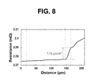
- FIG. 8 shows the results of measurement of contact resistance of the metalized p-type skutterudite thermoelectric material of FIG. 7 .
- FIG. 9 shows the results of EDS after thermal treatment of the metalized n-type skutterudite thermoelectric material of FIG. 5 at 500° C. for 10 hr
- FIG. 10 shows the results of measurement of contact resistance of the metalized n-type skutterudite thermoelectric material of FIG. 9 .
- thermoelectric device having high reliability can be confirmed to be obtained by forming the Fe—Ni layer between the skutterudite thermoelectric material and the Ti metalization layer.
- the metalization layer may crack. This is considered to be due to a difference in coefficient of thermal expansion between Fe or Ni when used alone and the skutterudite thermoelectric material.
- the Fe—Ni alloy is applied, a difference in coefficient of thermal expansion from the skutterudite thermoelectric material is small, and thus no cracking occurs.
- the Fe—Ni layer and the Ti layer, which constitute the Fe—Ni/Ti multilayered metalization structure are formed to respective thicknesses of 40 ⁇ m or more.
- the Ti layer may play a role in sufficiently performing a diffusion barrier function, and the Fe—Ni layer may satisfactorily function between the Ti layer and the skutterudite thermoelectric material and may also function as a thermal expansion buffer layer.
- the thickness of the Fe—Ni layer which is left behind after the formation of the intermetallic compound, may be 40 ⁇ m or more.
- the upper limits of the thicknesses of the Fe—Ni layer and the Ti layer are not particularly limited, and may be set to 150 ⁇ m or less in order to avoid increased material costs and because the properties may deteriorate when being excessively thick.
- forming the multilayered metalization structure on the surface of skutterudite may be conducted using a variety of conventional processes without limitation.
- individual layers of the multilayered metalization structure may be sequentially stacked and formed using various deposition processes and hot pressing, and metal foils are superimposed and may be metalized all at once through a process such as hot pressing.
- the multilayered metalization structure In addition to the formation of the multilayered metalization structure on the surface of the skutterudite thermoelectric material produced in the form of an ingot, it is possible to form the multilayered metalization structure by performing a hot pressing process while the skutterudite thermoelectric material in a powder phase is sintered and manufactured in the form of an ingot, as described above.
Landscapes
- Chemical & Material Sciences (AREA)
- Inorganic Chemistry (AREA)
- Engineering & Computer Science (AREA)
- Life Sciences & Earth Sciences (AREA)
- Wood Science & Technology (AREA)
- Manufacturing & Machinery (AREA)
- Powder Metallurgy (AREA)
Abstract
Description
Claims (9)
Applications Claiming Priority (2)
| Application Number | Priority Date | Filing Date | Title |
|---|---|---|---|
| KR10-2017-0046694 | 2017-04-11 | ||
| KR1020170046694A KR20180114694A (en) | 2017-04-11 | 2017-04-11 | Fe-Ni/Ti METALIZING METHOD FOR SKUTTERUDITE THERMOELECTRIC MATERIALS, Fe-Ni/Ti MULTILAYER METALIZING STRUCTURE FOR SKUTTERUDITE THERMOELECTRIC MATERIALS, SKUTTERUDITE THERMOELECTRIC MATERIALS WITH Fe-Ni/Ti MULTILAYER METALIZING STRUCTURE AND MANUFACTURING METHOD FOR THE SAME |
Publications (2)
| Publication Number | Publication Date |
|---|---|
| US20180294400A1 US20180294400A1 (en) | 2018-10-11 |
| US10147864B2 true US10147864B2 (en) | 2018-12-04 |
Family
ID=63711917
Family Applications (1)
| Application Number | Title | Priority Date | Filing Date |
|---|---|---|---|
| US15/695,006 Active US10147864B2 (en) | 2017-04-11 | 2017-09-05 | Fe—Ni/Ti metalized skutterudite thermoelectric material and method of manufacturing the same |
Country Status (2)
| Country | Link |
|---|---|
| US (1) | US10147864B2 (en) |
| KR (1) | KR20180114694A (en) |
Families Citing this family (4)
| Publication number | Priority date | Publication date | Assignee | Title |
|---|---|---|---|---|
| KR102144070B1 (en) * | 2018-12-31 | 2020-08-12 | 한국에너지기술연구원 | Ti METALIZING STRUCTURE FOR SKUTTERUDITE THERMOELECTRIC MATERIALS WITH ITO INTERLAYER, Ti METALIZING METHOD, SKUTTERUDITE THERMOELECTRIC MATERIALS WITH Ti METALIZING AND MANUFACTURING METHOD FOR THE SAME |
| KR102144071B1 (en) * | 2018-12-31 | 2020-08-12 | 한국에너지기술연구원 | Co-Mo COMPOSITE METALIZING METHOD FOR SKUTTERUDITE THERMOELECTRIC MATERIALS, Co-Mo COMPOSITE METALIZING STRUCTURE FOR SKUTTERUDITE THERMOELECTRIC MATERIALS, STRUCTURE AND MANUFACTURING METHOD FOR SKUTTERUDITE THERMOELECTRIC MATERIALS WITH Co-Mo COMPOSITE METALIZING |
| KR102245517B1 (en) * | 2019-04-05 | 2021-04-28 | 한국에너지기술연구원 | METALIZING METHOD FOR Bi2Te3 THERMOELECTRIC MATERIALS, Bi2Te3 THERMOELECTRIC MATERIALS WITH MIXED METALIZING STRUCTURE AND MANUFACTURING METHOD FOR THE SAME |
| KR102198279B1 (en) * | 2019-09-06 | 2021-01-05 | 한국에너지기술연구원 | Metalizing structure for skutterudite thermoelectric material including ito layer |
Citations (9)
| Publication number | Priority date | Publication date | Assignee | Title |
|---|---|---|---|---|
| US4855810A (en) | 1987-06-02 | 1989-08-08 | Gelb Allan S | Thermoelectric heat pump |
| KR20070004950A (en) | 2004-04-21 | 2007-01-09 | 쇼와 덴코 가부시키가이샤 | Process for producing Hussler alloy, semi-Hussor alloy, filled Scraterite-based alloy, and thermoelectric conversion system using the same |
| JP2010165847A (en) | 2009-01-15 | 2010-07-29 | Sumitomo Chemical Co Ltd | Method of manufacturing thermoelectric conversion module |
| US20140096809A1 (en) * | 2012-10-08 | 2014-04-10 | Samsung Electronics Co., Ltd. | Thermoelectric device, thermoelectric module including the thermoelectric device, thermoelectric apparatus including the thermoelectric module, and method of manufacturing the same |
| US20140109948A1 (en) * | 2012-10-19 | 2014-04-24 | Samsung Electronics Co., Ltd. | Thermoelectric module, thermoelectric device comprising the same, and process for preparing the thermoelectric element |
| US20150171304A1 (en) * | 2013-12-17 | 2015-06-18 | Evident Technologies | Thermoelectric Elements Including of Axially Dependent Material Properties |
| US20160163948A1 (en) | 2013-03-14 | 2016-06-09 | Gmz Energy, Inc. | Thermoelectric Device Fabrication Using Direct Bonding |
| KR20170011622A (en) | 2015-07-23 | 2017-02-02 | 서울시립대학교 산학협력단 | Thermoelectric Element using exothermic and amorphous bonding material And Method of Manufacturing The Same |
| JP2017045840A (en) | 2015-08-26 | 2017-03-02 | 古河電気工業株式会社 | Thermoelectric conversion element and thermoelectric conversion module |
-
2017
- 2017-04-11 KR KR1020170046694A patent/KR20180114694A/en not_active Ceased
- 2017-09-05 US US15/695,006 patent/US10147864B2/en active Active
Patent Citations (10)
| Publication number | Priority date | Publication date | Assignee | Title |
|---|---|---|---|---|
| US4855810A (en) | 1987-06-02 | 1989-08-08 | Gelb Allan S | Thermoelectric heat pump |
| KR20070004950A (en) | 2004-04-21 | 2007-01-09 | 쇼와 덴코 가부시키가이샤 | Process for producing Hussler alloy, semi-Hussor alloy, filled Scraterite-based alloy, and thermoelectric conversion system using the same |
| JP2010165847A (en) | 2009-01-15 | 2010-07-29 | Sumitomo Chemical Co Ltd | Method of manufacturing thermoelectric conversion module |
| US20110284523A1 (en) * | 2009-01-15 | 2011-11-24 | Sumitomo Chemical Company, Limited | Method for manufacturing thermoelectric conversion module |
| US20140096809A1 (en) * | 2012-10-08 | 2014-04-10 | Samsung Electronics Co., Ltd. | Thermoelectric device, thermoelectric module including the thermoelectric device, thermoelectric apparatus including the thermoelectric module, and method of manufacturing the same |
| US20140109948A1 (en) * | 2012-10-19 | 2014-04-24 | Samsung Electronics Co., Ltd. | Thermoelectric module, thermoelectric device comprising the same, and process for preparing the thermoelectric element |
| US20160163948A1 (en) | 2013-03-14 | 2016-06-09 | Gmz Energy, Inc. | Thermoelectric Device Fabrication Using Direct Bonding |
| US20150171304A1 (en) * | 2013-12-17 | 2015-06-18 | Evident Technologies | Thermoelectric Elements Including of Axially Dependent Material Properties |
| KR20170011622A (en) | 2015-07-23 | 2017-02-02 | 서울시립대학교 산학협력단 | Thermoelectric Element using exothermic and amorphous bonding material And Method of Manufacturing The Same |
| JP2017045840A (en) | 2015-08-26 | 2017-03-02 | 古河電気工業株式会社 | Thermoelectric conversion element and thermoelectric conversion module |
Non-Patent Citations (2)
| Title |
|---|
| Byeongcheol Song et al., "The effects of diffusion barrier layers on the microstructural and electrical properties in CoSb3 thermoelectric modules", Journal of Alloys and Compounds, Jul. 16, 2014, pp. 160-162, vol. 617, Elsevier B.V. |
| Korean Office Action for corresponding Korean Patent Application No. 10-2017-0046694 dated Aug. 13, 2018. |
Also Published As
| Publication number | Publication date |
|---|---|
| US20180294400A1 (en) | 2018-10-11 |
| KR20180114694A (en) | 2018-10-19 |
Similar Documents
| Publication | Publication Date | Title |
|---|---|---|
| US10147864B2 (en) | Fe—Ni/Ti metalized skutterudite thermoelectric material and method of manufacturing the same | |
| KR102094995B1 (en) | Thermoelectric module, thermoelectric device comprising the same, and process for preparing the thermoelectric element | |
| JP5212937B2 (en) | Thermoelectric conversion element, thermoelectric module including the thermoelectric conversion element, and method for manufacturing thermoelectric conversion element | |
| JP2012522380A (en) | Thermoelectric conversion element, electrode material and manufacturing method thereof | |
| CN107427967B (en) | Method for preprocessing semiconducting thermoelectric materials for metallization, interconnection and bonding | |
| JP6164569B2 (en) | Thermoelectric element and method for manufacturing thermoelectric element | |
| KR20170076358A (en) | Thermoelectric module and method for fabricating the same | |
| US10224472B2 (en) | Thermoelectric power module | |
| KR102487993B1 (en) | Thermoelectric module | |
| CN104321889B (en) | Thermo-electric converting material and use its thermo-electric conversion module and its manufacture method | |
| KR102311803B1 (en) | Anti-diffusion layer of thermoelectric material and manufacturing method thereof | |
| JP6404983B2 (en) | Thermoelectric module | |
| CN106252500B (en) | A cobalt antimonide-based thermoelectric element and its preparation method | |
| JP7087519B2 (en) | Manufacturing method of thermoelectric element, thermoelectric conversion module and thermoelectric element | |
| KR101323097B1 (en) | Thermoelectric device with copper electrode and manufacturing method of the same | |
| KR102340798B1 (en) | Thermoelectric element and module thermoelectric module comprising the same | |
| KR102129050B1 (en) | Thermoelectric module | |
| KR102144070B1 (en) | Ti METALIZING STRUCTURE FOR SKUTTERUDITE THERMOELECTRIC MATERIALS WITH ITO INTERLAYER, Ti METALIZING METHOD, SKUTTERUDITE THERMOELECTRIC MATERIALS WITH Ti METALIZING AND MANUFACTURING METHOD FOR THE SAME | |
| KR102144071B1 (en) | Co-Mo COMPOSITE METALIZING METHOD FOR SKUTTERUDITE THERMOELECTRIC MATERIALS, Co-Mo COMPOSITE METALIZING STRUCTURE FOR SKUTTERUDITE THERMOELECTRIC MATERIALS, STRUCTURE AND MANUFACTURING METHOD FOR SKUTTERUDITE THERMOELECTRIC MATERIALS WITH Co-Mo COMPOSITE METALIZING | |
| CN107210354B (en) | Method of manufacturing a sealed thermoelectric module | |
| KR102198279B1 (en) | Metalizing structure for skutterudite thermoelectric material including ito layer | |
| JP2001189497A (en) | Thermoelectric conversion element and manufacturing method therefor | |
| KR20180114695A (en) | Metalizing method for skutterudite thermoelectric materials, multilayer metalizing structure for skutterudite thermoelectric materials, skutterudite thermoelectric materials with multilayer metalizing structure and manufacturing method for the same | |
| WO2016088762A2 (en) | Silicide-based thermoelectric power generation element | |
| KR102070644B1 (en) | Mixed metalizing structure for skutterudite thermoelectric materials, metalizing method for skutterudite thermoelectric materials, skutterudite thermoelectric materials with mixed metalizing structure and manufacturing method for the same |
Legal Events
| Date | Code | Title | Description |
|---|---|---|---|
| AS | Assignment |
Owner name: KOREA INSTITUTE OF ENERGY RESEARCH, KOREA, REPUBLI Free format text: ASSIGNMENT OF ASSIGNORS INTEREST;ASSIGNORS:PARK, SANG HYUN;YOO, CHUNG-YUL;JIN, YOUNG HWAN;AND OTHERS;REEL/FRAME:043761/0664 Effective date: 20170828 Owner name: KOREA ADVANCED INSTITUTE OF SCIENCE AND TECHNOLOGY Free format text: ASSIGNMENT OF ASSIGNORS INTEREST;ASSIGNORS:PARK, SANG HYUN;YOO, CHUNG-YUL;JIN, YOUNG HWAN;AND OTHERS;REEL/FRAME:043761/0664 Effective date: 20170828 |
|
| FEPP | Fee payment procedure |
Free format text: ENTITY STATUS SET TO UNDISCOUNTED (ORIGINAL EVENT CODE: BIG.); ENTITY STATUS OF PATENT OWNER: SMALL ENTITY |
|
| FEPP | Fee payment procedure |
Free format text: ENTITY STATUS SET TO SMALL (ORIGINAL EVENT CODE: SMAL); ENTITY STATUS OF PATENT OWNER: SMALL ENTITY |
|
| STCF | Information on status: patent grant |
Free format text: PATENTED CASE |
|
| MAFP | Maintenance fee payment |
Free format text: PAYMENT OF MAINTENANCE FEE, 4TH YR, SMALL ENTITY (ORIGINAL EVENT CODE: M2551); ENTITY STATUS OF PATENT OWNER: SMALL ENTITY Year of fee payment: 4 |