US10141865B1 - Hybrid CHB-TVSI multilevel voltage source inverter - Google Patents
Hybrid CHB-TVSI multilevel voltage source inverter Download PDFInfo
- Publication number
- US10141865B1 US10141865B1 US15/823,192 US201715823192A US10141865B1 US 10141865 B1 US10141865 B1 US 10141865B1 US 201715823192 A US201715823192 A US 201715823192A US 10141865 B1 US10141865 B1 US 10141865B1
- Authority
- US
- United States
- Prior art keywords
- output
- power
- bridge
- units
- phase
- Prior art date
- Legal status (The legal status is an assumption and is not a legal conclusion. Google has not performed a legal analysis and makes no representation as to the accuracy of the status listed.)
- Expired - Fee Related
Links
Images


Classifications
-
- H—ELECTRICITY
- H02—GENERATION; CONVERSION OR DISTRIBUTION OF ELECTRIC POWER
- H02M—APPARATUS FOR CONVERSION BETWEEN AC AND AC, BETWEEN AC AND DC, OR BETWEEN DC AND DC, AND FOR USE WITH MAINS OR SIMILAR POWER SUPPLY SYSTEMS; CONVERSION OF DC OR AC INPUT POWER INTO SURGE OUTPUT POWER; CONTROL OR REGULATION THEREOF
- H02M7/00—Conversion of ac power input into dc power output; Conversion of dc power input into ac power output
- H02M7/42—Conversion of dc power input into ac power output without possibility of reversal
- H02M7/44—Conversion of dc power input into ac power output without possibility of reversal by static converters
- H02M7/48—Conversion of dc power input into ac power output without possibility of reversal by static converters using discharge tubes with control electrode or semiconductor devices with control electrode
- H02M7/483—Converters with outputs that each can have more than two voltages levels
-
- H—ELECTRICITY
- H02—GENERATION; CONVERSION OR DISTRIBUTION OF ELECTRIC POWER
- H02M—APPARATUS FOR CONVERSION BETWEEN AC AND AC, BETWEEN AC AND DC, OR BETWEEN DC AND DC, AND FOR USE WITH MAINS OR SIMILAR POWER SUPPLY SYSTEMS; CONVERSION OF DC OR AC INPUT POWER INTO SURGE OUTPUT POWER; CONTROL OR REGULATION THEREOF
- H02M1/00—Details of apparatus for conversion
- H02M1/0095—Hybrid converter topologies, e.g. NPC mixed with flying capacitor, thyristor converter mixed with MMC or charge pump mixed with buck
-
- H—ELECTRICITY
- H02—GENERATION; CONVERSION OR DISTRIBUTION OF ELECTRIC POWER
- H02M—APPARATUS FOR CONVERSION BETWEEN AC AND AC, BETWEEN AC AND DC, OR BETWEEN DC AND DC, AND FOR USE WITH MAINS OR SIMILAR POWER SUPPLY SYSTEMS; CONVERSION OF DC OR AC INPUT POWER INTO SURGE OUTPUT POWER; CONTROL OR REGULATION THEREOF
- H02M7/00—Conversion of ac power input into dc power output; Conversion of dc power input into ac power output
- H02M7/42—Conversion of dc power input into ac power output without possibility of reversal
- H02M7/44—Conversion of dc power input into ac power output without possibility of reversal by static converters
- H02M7/48—Conversion of dc power input into ac power output without possibility of reversal by static converters using discharge tubes with control electrode or semiconductor devices with control electrode
- H02M7/483—Converters with outputs that each can have more than two voltages levels
- H02M7/4835—Converters with outputs that each can have more than two voltages levels comprising two or more cells, each including a switchable capacitor, the capacitors having a nominal charge voltage which corresponds to a given fraction of the input voltage, and the capacitors being selectively connected in series to determine the instantaneous output voltage
-
- H—ELECTRICITY
- H02—GENERATION; CONVERSION OR DISTRIBUTION OF ELECTRIC POWER
- H02M—APPARATUS FOR CONVERSION BETWEEN AC AND AC, BETWEEN AC AND DC, OR BETWEEN DC AND DC, AND FOR USE WITH MAINS OR SIMILAR POWER SUPPLY SYSTEMS; CONVERSION OF DC OR AC INPUT POWER INTO SURGE OUTPUT POWER; CONTROL OR REGULATION THEREOF
- H02M7/00—Conversion of ac power input into dc power output; Conversion of dc power input into ac power output
- H02M7/42—Conversion of dc power input into ac power output without possibility of reversal
- H02M7/44—Conversion of dc power input into ac power output without possibility of reversal by static converters
- H02M7/48—Conversion of dc power input into ac power output without possibility of reversal by static converters using discharge tubes with control electrode or semiconductor devices with control electrode
- H02M7/483—Converters with outputs that each can have more than two voltages levels
- H02M7/49—Combination of the output voltage waveforms of a plurality of converters
-
- H—ELECTRICITY
- H02—GENERATION; CONVERSION OR DISTRIBUTION OF ELECTRIC POWER
- H02M—APPARATUS FOR CONVERSION BETWEEN AC AND AC, BETWEEN AC AND DC, OR BETWEEN DC AND DC, AND FOR USE WITH MAINS OR SIMILAR POWER SUPPLY SYSTEMS; CONVERSION OF DC OR AC INPUT POWER INTO SURGE OUTPUT POWER; CONTROL OR REGULATION THEREOF
- H02M7/00—Conversion of ac power input into dc power output; Conversion of dc power input into ac power output
- H02M7/42—Conversion of dc power input into ac power output without possibility of reversal
- H02M7/44—Conversion of dc power input into ac power output without possibility of reversal by static converters
- H02M7/48—Conversion of dc power input into ac power output without possibility of reversal by static converters using discharge tubes with control electrode or semiconductor devices with control electrode
- H02M7/53—Conversion of dc power input into ac power output without possibility of reversal by static converters using discharge tubes with control electrode or semiconductor devices with control electrode using devices of a triode or transistor type requiring continuous application of a control signal
- H02M7/537—Conversion of dc power input into ac power output without possibility of reversal by static converters using discharge tubes with control electrode or semiconductor devices with control electrode using devices of a triode or transistor type requiring continuous application of a control signal using semiconductor devices only, e.g. single switched pulse inverters
- H02M7/5387—Conversion of dc power input into ac power output without possibility of reversal by static converters using discharge tubes with control electrode or semiconductor devices with control electrode using devices of a triode or transistor type requiring continuous application of a control signal using semiconductor devices only, e.g. single switched pulse inverters in a bridge configuration
- H02M7/53871—Conversion of dc power input into ac power output without possibility of reversal by static converters using discharge tubes with control electrode or semiconductor devices with control electrode using devices of a triode or transistor type requiring continuous application of a control signal using semiconductor devices only, e.g. single switched pulse inverters in a bridge configuration with automatic control of output voltage or current
-
- H—ELECTRICITY
- H02—GENERATION; CONVERSION OR DISTRIBUTION OF ELECTRIC POWER
- H02M—APPARATUS FOR CONVERSION BETWEEN AC AND AC, BETWEEN AC AND DC, OR BETWEEN DC AND DC, AND FOR USE WITH MAINS OR SIMILAR POWER SUPPLY SYSTEMS; CONVERSION OF DC OR AC INPUT POWER INTO SURGE OUTPUT POWER; CONTROL OR REGULATION THEREOF
- H02M1/00—Details of apparatus for conversion
- H02M1/0067—Converter structures employing plural converter units, other than for parallel operation of the units on a single load
- H02M1/007—Plural converter units in cascade
-
- H02M2001/007—
Definitions
- the disclosure of the present application relates to electrical power derived from renewable energy sources (such as solar power and wind power), and in particular to a hybrid CHB-TVSI multilevel voltage source inverter that combines a cascaded H-bridge (CHB) multilevel inverter (MLI) with a three-phase voltage source inverter (TVSI) to connect multiple DC sources to an electrical grid.
- renewable energy sources such as solar power and wind power
- CHB-TVSI multilevel voltage source inverter that combines a cascaded H-bridge (CHB) multilevel inverter (MLI) with a three-phase voltage source inverter (TVSI) to connect multiple DC sources to an electrical grid.
- the inverter can be classified according to the number of voltage levels generated into two groups, the two-level inverter and the multilevel inverter (MLI).
- MLI multilevel inverter
- many multilevel converter topologies have been proposed and gained attention in many applications, especially in the interface for grid connection of PV system applications.
- the most common MLI topologies can be classified into three types, viz., neutral point MLI, flying capacitor MLI, and cascaded H-bridge.
- a three-level neutral point clamping topology was implemented as far back as 1981.
- Four, five, and six levels have been proposed for use in static VAR compensation, variable speed motor drives, and high voltage system interconnections.
- the neutral point clamping converter has many advantages, such as that the voltage can be shared between switches, smaller output current ripples, a plentiful supply of IGBT modules for a leg or the whole of the NPC inverter in the market, and that the topology does not need isolated DC sources.
- the NPC also have some disadvantages, such as an increase in the number of clamping diodes with an increasing number of levels, which makes the inverter bulky. In addition, increasing the number of levels leads to an increase in diode losses. On the other hand, the clamping diodes require different voltage ratings for reverse recovery blocking.
- the flying capacitor (FC) multilevel topology is considered an alternative to the NPC topology, with capacitor MLI also proposed. Flying capacitor topology is similar to NPC topology, except that capacitors are added instead of diodes.
- the FC MLI provides many advantages over the NPC, such as eliminating the clamping diodes presented in the NPC, and there is no need for filters due to the presence of capacitors. However, with an increase in the number of levels, control of charging and discharging the capacitors of the FC MLI will not be easy, and the cost will increase. In addition, this topology needs more capacitors compared with NPC, and it will be bulky with increasing the number of levels.
- MMC Although MMC topologies have received more attention in many applications, the technology has some drawbacks. In MMC, losses are not evenly distributed among switches of submodules of the MMC arms. This property of MMC topology is not related to the modulation technique used. On the other hand, in the case of cascaded H-bridge MLI, using phase shift pulse width modulation PWM (PSPWM) modulation technique causes equal sharing of losses among different switches. Unequal sharing of losses among MMC switches results in unequal junction temperature, and this will cause the need for using higher IGBTs rating. From another point of view, MMC needs much more installed capacitance in comparison to the CHB, and this is one of the main drawbacks of the MMC topology.
- PWM phase shift pulse width modulation
- MPPT Maximum power point tracking
- PV photovoltaic
- FIGS. 1-7 Examples of multi-layer inverters are shown in FIGS. 1-7 .
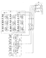
- FIG. 1 is a schematic diagram showing a prior art three-phase, five-level cascaded H-bridge multilevel inverter.
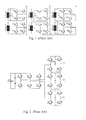
- FIG. 2 is a schematic diagram showing a prior art hybrid multilevel inverter topology.
- FIG. 3 is a schematic diagram showing a prior art nine-level hybrid multilevel inverter topology.
- FIG. 4 is a schematic diagram that shows a prior art modular multilevel inverter topology.
- FIG. 5 is a schematic diagram showing a prior art new topology based on modular multilevel inverter topology.
- FIG. 6 is a schematic diagram showing a hybrid topology based on a modular multilevel inverter and a conventional two-level inverter.
- cascaded MLI topology is based on the conventional two-level voltage source inverter and has attractive features in many applications, especially for motor drive applications.
- This cascaded MLI can also be used for grid-connected renewable energy applications.
- One technique uses this topology to connect a wind farm to the grid.
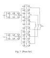
- Another technique uses the multilevel VSI cascaded inverter for grid-connected PV applications, as shown in FIG. 7 .
- the limitations in this triple cascaded VSI is that it is not possible to increase the number of cascaded inverter units more than three, and therefore the number of levels will be limited.
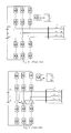
- the hybrid CHB-TVSI multilevel voltage source inverter is configured with an upper part and a lower part.
- the upper part includes a set of pairs of H-bridge cells having pairs of x-side and y-side switched intermediate outputs, the cells being cascaded such that a terminal between the y-side switched intermediate output on one side of the first H-bridge cell connects with a terminal between the x-side switched intermediate output of the second H-bridge cell, and a terminal between the y-side switched intermediate output on one side of the second H-bridge cell connects with a terminal between the x-side switched intermediate output of the next H-bridge cell.
- the respective H-bridges in the upper part are connected to one or more DC power sources, which are connected in series or parallel to track a desired input voltage to feed the respective H-bridge.
- the H-bridge cells have a first set of outputs connected to each other, and a second set of outputs provide output power in respective phases. In one configuration the second set of outputs provides output power to a first set of primary winding connections on respective phases of the set of output transformers.
- a lower part includes a polyphase voltage source inverter having a number of phases corresponding to the number of phases in the upper part, such as three phases.
- the lower part includes a number of units corresponding to the phases and connected to one or more DC power sources.
- Each of the units is provided as a three-leg, two-level inverter connected in cascade, each unit having three output terminals. Two of the output terminals of the units in the lower part are connected to respective output terminals of other units of the lower part, and one of the output terminals of the units in the lower part is connected to the upper part.
- the connections of the upper and lower parts connect respective phases of the upper part to corresponding phases of the lower part.
- the inverter system is configured as three-phase.
- the upper and lower phases are linked through inductive couplings, and in other configurations, the upper and lower phases are directly connected.
- FIG. 1 is a schematic diagram of a three-phase, five-level cascaded H-bridge multilevel inverter of the prior art.
- FIG. 2 is a schematic diagram of a hybrid multilevel inverter topology of the prior art.
- FIG. 3 is a schematic diagram of a nine-level hybrid multilevel inverter topology of the prior art.
- FIG. 4 is a schematic diagram of a modular multilevel inverter topology of the prior art.
- FIG. 5 is a schematic diagram of a new topology of the prior art based on modular multilevel inverter topology.
- FIG. 6 is a schematic diagram of a hybrid topology of the prior art based on modular multilevel inverter and conventional two-level inverter.
- FIG. 7 is a schematic diagram of a cascaded three-phase triple voltage source inverter topology of the prior art.
- FIG. 8 is a schematic diagram of a hybrid CHB-TVSI multilevel voltage source inverter according to the present disclosure.
- FIG. 9 is a schematic diagram of a single H-bridge cell used in the hybrid CHB-TVSI multilevel voltage source inverter of FIG. 8 .
- FIG. 10 is a schematic diagram of the cascaded H-bridge inverter, in phase a.
- FIG. 11 is a schematic diagram of a DC-DC ⁇ uk converter.
- FIG. 12 is a schematic diagram of a three-phase, two-level VSI.
- FIG. 13 is a schematic diagram of an embodiment of a hybrid CHB-TVSI multilevel voltage source inverter according to the present disclosure having a direct connection.
- FIG. 14 is a schematic diagram of a control scheme for a hybrid CHB-TVSI multilevel voltage source inverter according to the present disclosure.
- FIG. 15 is a waveform diagram showing the modulation signals for a hybrid CHB-TVSI multilevel voltage source inverter according to the present disclosure.
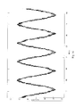
- FIG. 16 is a plot of the multilevel voltage generated across the primary side of transformer T 1 , va1a2, in phase a of the hybrid CHB-TVSI multilevel voltage source inverter of FIG. 8 .
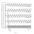
- FIG. 17 is a plot of the three-phase voltages generated by the disclosed topology across the primary sides of the transformers T 1 , T 2 and T 3 of the hybrid CHB-TVSI multilevel voltage source inverter of FIG. 8 .
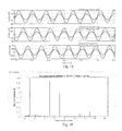
- FIG. 18 is a waveform diagram of the three-phase grid voltages and currents of the hybrid CHB-TVSI multilevel voltage source inverter of FIG. 8 .
- FIG. 19 is a plot of THD of the grid current, phase a, of the hybrid CHB-TVSI multilevel voltage source inverter of FIG. 8 .
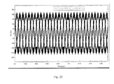
- FIG. 20 is a plot of the three-phase voltages generated by the direct-connection topology of the hybrid CHB-TVSI multilevel voltage source inverter of FIG. 13 .
- the hybrid CHB-TVSI multilevel voltage source inverter is a grid-connected multilevel inverter topology that can be used for different applications.
- the disclosed subject matter introduces a combination of cascaded H-bridge multilevel inverter with a cascaded three-phase voltage source inverter, the latter also called a three-phase triple voltage source inverter (TVSI).
- This combination increases the number of voltage levels generated using a lower component count compared as to the conventional multilevel inverter topologies for the same voltage levels generated.
- This configuration also assures a continuous power supply to the grid in case of failure of one part in the disclosed configuration.
- the three-phase VSI unit part can be isolated from the grid and the cascaded H-bridge MLI part stills works at lower voltage levels to reduce the fault current shared from the inverter system.
- the cascaded H-bridge units (upper part) are directly connected to the corresponding phase in the three-phase triple VSI units (lower part).
- the direct connection topology is introduced in order to improve system performance and reduce the system cost.
- the number of voltage levels generated from the extension topology is also higher while using a lower number of component compared to the other conventional MLI topologies to generate the same voltage levels.
- Both topologies are built in MATLAB/SIMULINK environment. Simulation results and comparisons are presented to validate the disclosed topologies.
- the disclosure focuses on a multilevel inverter topology for grid-connected applications, and in particular connecting PV (photovoltaic) systems to a grid PV system.
- cascaded H-bridge topologies have received more attention.
- the cascaded H-bridge inverter has a simple layout, extreme modularity, is easy in construction and control, has reduced voltage balance problems, and compared to the other multilevel topologies, requires the least number of components to generate the same voltage levels.
- the cascaded H-bridge MLI is an attractive approach for a grid-connected PV system. DC sources can be replaced by a PV module/array, and due to the separated DC link feature, voltage control becomes possible.
- MPPT maximum power point tracking
- a cascaded H-bridge multilevel inverter is based on series connection of H-bridge cells. It is an alternative topology with a lower number of components compared with the other MLI topologies of the same level. Each H-bridge cell can be used to generate three voltage levels by unipolar modulation technique. Each H-bridge cell has a separated DC source. Cascaded H-bridge MLI topology has the least number of components in comparison with other topologies at the same level, ease of control, no voltage balancing problem, ease of construction, reliable and low inverter cost.
- cascaded MLI features presents an attractive approach for many applications, such as use CHB MLI in standalone systems, some of the in static VAR compensations, and some of them use CHB MLI in grid-connected PV system.
- Cascaded H-bridge multilevel inverter requires an isolated DC source for each H-bridge. Therefore, a combination of the multiple H-bridge modules would favor this topology in medium and large grid-connected PV systems.
- CHB multilevel inverters also overcome some of the drawbacks inherent in MMC topologies.
- MPPT control is particularly useful in PV modules.
- PV module behavior is not linear in nature as a result of the effects of environmental conditions, and hence exhibits nonlinear PV curves.
- MPP maximum power point
- MPPT maximum power point tracking
- MPPT in association with PV modules is achieved by connecting the PV modules to DC-DC converters. The voltage and the current of the PV module is then measured, and the power is calculated.
- the MPPT as in the Perturb and Observe MPPT method—perturbs the voltage and observes the power to determine the change direction. If the power difference is positive, the direction of perturbation remains the same. Otherwise, it is reversed. Finally, the MPPT generates the required switching signal to drive the IGBTs of the DC-DC converters in order to keep operating the PV module at its maximum power.
- the hybrid CHB-TVSI multilevel voltage source inverter comprises two parts, which are connected together by open-end winding transformers.
- the topology is shown in shown in FIG. 8 .
- the topology can be divided it into “upper” and “lower” parts.
- the upper part is the cascaded H-bridge MLI, and the lower part is the three-phase triple VSI.
- the upper part is configured as a three-phase system.
- Each phase comprises N H-bridge cells.
- a single H-bridge cell is shown in FIG. 9 .
- These cells are cascaded, as shown in FIG. 10 , such that the a y1 terminal of the H-bridge cell 1 in phase a, for example, is connected to the a x2 terminal of the next H-bridge cell.
- the a y(N ⁇ 1) terminal is connected to the a xN terminal of the last H-bridge cell.
- the same approach is applied to phases b and c.
- the terminals a yN , b yN and c yN of phases a, b, and c are connected together to one point NN.
- the cascaded H-bridge is based on the AC module topology in which only one converter is used per module due the fact that the AC module topology is superior over the other types, since it is the most modular and has the best MPPT capability.
- Each H-bridge cell in the upper part is connected to n umber of PV modules via DC-DC converters.
- Each PV module is connected to one DC-DC converter.
- the output terminals of the DC-DC converters are then connected in series/parallel to obtain the desired input voltage/current level to feed the H-bridge cell.
- the reason of using one DC-DC converter per module is to track the maximum power for only one PV module. This helps in achieving the best MPPT of the PV modules.
- the DC-DC converter used here is the ⁇ uk converter, shown in FIG. 11 .
- the lower part is configured as a three-phase system, corresponding to the number of phases in the upper part.
- the three-phase triple voltage source multilevel inverter comprises three units. Each unit is a three-leg, two-level inverter, as shown in FIG. 12 .
- the three units are cascaded, as shown in the lower part of FIG. 8 .
- Each unit comprises three terminals, where a 21 , b 21 , and c 21 are the output terminals of unit 1 and a 22 , b 22 , and c 22 are the output terminals of unit 2 , while a 23 , b 23 , and c 23 are the output terminals of unit 3 .
- the PV modules are connected to each VSI unit via a DC-DC converter.
- the upper and the lower parts are connected in such a way that phase A of the upper configuration is connected to phase A of the lower configuration via open-end winding transformer, etc., for all phases. That is, in the case of the three-phase architecture, terminal a x1 from the upper part is connected to the terminal a 1 of the open-end winding transformer T 1 , while terminal a 21 of unit 1 in the lower part is connected to terminal a 2 of the open-end winding transformer T 1 .
- the terminal b x1 of the upper part is connected to the terminal b 1 of the open-end winding transformer T 2
- terminal b 22 of unit 2 in the lower part is connected to terminal b 2 of the open-end winding transformer T 2 .
- terminal c x1 of the upper part is connected to terminal c 1 of the open-end winding transformer T 3
- terminal c 23 of unit 3 in the lower part is connected to terminal c 2 of the open-end winding transformer T 3 .
- the secondary windings of the transformers T 1 , T 2 and T 3 are then connected to the three phase grid.
- Three single-phase line frequency transformers presented in the disclosed technique are used to connect the upper three-phase cascaded H-bridge inverter with the lower three-phase triple voltage source inverter. The operation of the three single-phase transformers is based on the principles of the open-end transformer.
- the voltage rating of the power devices is reduced by half; (2) the size of the capacitors is reduced; and (3) the DC bus magnitude that is provided by the PV modules can be reduced by half, as compared to if only one part (upper or lower) is used.
- This new topology generates a higher number of voltage levels while reducing the number of required switches, compared to conventional multilevel inverter topologies, to generate the same voltage levels. The reduction in the number of switches leads to reduced complexity and dimensions of the converter.
- the topology helps in reducing the THD of the voltages and currents. In case of failure in one part, the other part is working independently and power is still available.
- the number of H-bridge cells in the upper part can be increased. The presented concept is validated by means of simulation results.
- V is the RMS line-line grid voltage
- n is the number of cascaded H-bridges.
- the lower configuration can be isolated form the grid and the upper still working at lower voltage level to reduce the fault current sharing by the inverter system.
- v ab ( v a1 ⁇ v b1 ) ⁇ ( v a2 ⁇ v b2 )
- v bc ( v b1 ⁇ v c1 ) ⁇ ( v b2 ⁇ v c2 )
- v ca ( v c1 ⁇ v a1 ) ⁇ ( v c2 ⁇ v a2 ) (7)
- phase currents of the VSC in the lower part of FIG. 8 satisfy the following equations:
- Equation (18) defines the phase currents injected into the grid.
- the phase currents in the lower part can be defined as:
- Single-phase line frequency transformers corresponding to a polyphase configuration are used.
- three single-phase line frequency transformers presented in the disclosure are used to connect the upper cascaded H-bridge MLI with the lower three-phase cascaded voltage source inverter (triple voltage source inverter) by means of the open-end winding principle.
- the line frequency transformers are operating based on the principle of the open-end winding.
- An alternative approach can be made without using line frequency transformers, as shown in FIG. 13 .
- the neutral of each phase in the cascaded H-bridge units is directly connected to the corresponding phase in the three-phase triple VSI (lower part). That is, the neutral of phase a, a yN terminal, of the cascaded H-bridge part (upper part) is directly connected to the phase a, a 21 terminal, of the three-phase triple VSI (lower part).
- the neutral of phase b, b yN terminal, of the cascaded H-bridge part is directly connected to the phase b, b 22 terminal, of the three-phase triple VSI part.
- the neutral of phase c, c yN terminal, of the cascaded H-bridge part is directly connected to the phase c, c 23 terminal, of the three-phase triple VSI part.
- the three-phase direct-connection topology comprises N H-bridge units cascaded and directly connected to the three-phase two level voltage source inverter units, which are also cascaded.
- the three terminals a 1 , b 1 , and c 1 of phases a, b, and c of the direct-connection topology are then directly connected to the three-phase grid with using a lower number of components count when compared with the conventional multilevel inverter topologies to generate the same voltage level.
- no line frequency transformers are used in this direct-connection topology. This will reduce the total cost of the system and eliminate the drawback of the line frequency transformers. Therefore, in order to obtain an isolation in the direct connection topology; an isolated DC-DC converter can be used instead.
- v sAB U AB ⁇ ( j ⁇ L s ) i A +( j ⁇ L s ) i B
- v sBC U BC ⁇ ( j ⁇ L s ) i B +( j ⁇ L s ) i C
- v sCA U CA ⁇ ( j ⁇ L s ) i C +( j ⁇ L s ) i A
- v sAB v sA ⁇ v sB
- v sBC v sB ⁇ v sC
- sCA v sC ⁇ v sA .
- v sA ⁇ square root over (2) ⁇ V sin ⁇ t
- v sB ⁇ square root over (2) ⁇ Vs sin( ⁇ t ⁇ 120°)
- v sC ⁇ square root over (2) ⁇ V sin( ⁇ t+120°)
- V is the RMS phase voltages of the grid
- ⁇ is the frequency of the voltage in radians
- i A is the current injected to the grid, phase a
- i B is the current injected to the grid, phase b
- i C is the current injected to the grid, phase c.
- the three phase currents of the direct-connection topology can be written as:
- phase currents in the lower configuration can be defined as:
- the DC-DC converter shown in FIG. 10 is used for tracking the maximum power of the PV module.
- the main aim of the inverter controller is to generate reference currents in the synchronous frame such that the hybrid CHB-TVSI provides only available active power at the DC links to the grid with zero reactive power to guarantee unity power factor.
- the inverter control scheme has been extended to control the disclosed multilevel inverter. The disclosed control scheme is shown in FIGS. 13 and 14 .
- the DC voltage across the capacitors C dc1 , C dc2 , . . . , C dcN in each phase in the upper configuration is measured and compared with the reference voltage.
- each H-bridge unit is assumed to be Vref/N, where N is the number of H-bridge cells, which are cascaded in each phase, and Vref is the reference voltage of each VSI unit in the lower configuration.
- the DC links C dcA1 , C dcA2 , . . . , C dcAN and C dc3 share the same active grid current of phase a.
- the DC links C dcB1 , C dcB2 , . . . , C dcBN and C dc4 share the same active grid current of phase b.
- the DC links C dcC1 , C dcC2 , . . . , C dcCN and C dc5 share the same active grid current of phase c. Therefore, the comparison error signal of voltages across DC links C dcA1 , C dcA2 , . . .
- C dcAN and C dc3 with their respective reference voltages are summed and then passed to one PI (proportional integral) voltage controller.
- the result signal is u dca .
- the result signal from comparison of the voltages across DC links of phases b and c with their respective reference voltages are u dcb and u dcc , respectively.
- V mn - V Am + V Bm + V Cm 3 . ( 26 )
- the switching function C K of the inverter can be given as:
- V Am V Bm V Cm [ C A C B C C ] ⁇ [ V d ⁇ ⁇ c ⁇ ⁇ A V d ⁇ ⁇ c ⁇ ⁇ B V d ⁇ ⁇ cC ] , ( 27 ) where V dcA is the equivalent DC voltage across the DC link capacitors C dcA1 , C dcA2 , . . . , C dcAN and C dc3 in the hybrid CHB-TVSI topology.
- V dcB is the equivalent DC voltage across the DC link capacitors C dcB , C dcB2 , . . . , C dcBN and C dc4
- V dcC is the equivalent DC voltage across the DC link capacitors C dcC1 , C dcC2 , . . . , C dcCN and C dc5 .
- Equation (28) can be written as:
- V mn - 1 3 ⁇ ( C A + C B + C C ) ⁇ V dctot .
- v sA ( j ⁇ L s ) i A +d nA
- v sC ( j ⁇ L s ) i C +d nC V dctot (31)
- d nX is defined as the sequential function and is given by:
- Equation (31) can be written in the dq frame, and it is given as:
- the DC current can be defined as:
- This i d current is the active current, which is responsible to regulate the DC link capacitors, e.g., Cdc1a, Cdc2a and Cdc3. Therefore, it can be written as:
- the reference active current of the grid is the sum of the three id active currents:
- FIG. 14 The disclosed control scheme based on the analysis above is shown in FIG. 14 .
- the reference active current of the grid i dref is compared with the actual active grid current i d .
- the resulting signals, d nd and d nq obtained from equation (35), are transformed into abc reference voltage signals (V refa , V refb , and V refc ). These signals are then used to generate switching pulses to drive the IGBTs of the hybrid CHB-TVSI topology by comparing them with the generated triangular carrier waveforms.
- FIG. 15 is a graphical depiction, showing the modulation signals.
- the phase shift technique is used to generate the pulses to drive IGBTs of the cascaded H-bridge part (upper part), since the triangular signal of the next H-bridge cell is shifted from the previous H-bridge cell by 180/N, where N is the number of H-bridge cells.
- the reference voltage signal, V refa is compared with these phase-shifted triangular waveforms, and the resulting pulses are used to drive IGBTs of the H-bridge cells of phase a.
- the reference voltage signals V refb and V refc are also compared with the phase-shifted triangular waveforms to drive IGBTs of the H-bridge cells of phases b and c, respectively, of the upper part.
- phase-shifted triangular waveforms used to drive IGBTs of H-bridge cells of phase a are shown in FIG. 15 .
- the reference voltage signals V refa , V refb , and V refc are compared with the phase-shifted triangular waveforms, as shown in FIG. 15 .
- the triangular signal used to generated PWM pulses of unit 2 is shifted by (T/3) from that of unit 1
- the triangular signal used to generate PWM pulses of unit 3 is shifted by (T/3) from that of unit 2 .
- the generated triangular waveforms of the lower part are shifted from the last triangular signal of H-bridge cell number N in the upper part by (T/(N+1)), where N is the number of H-bridge cells in the upper part of the hybrid CHB-TVSI topology.
- the system comprises 24 HIT-N220A01 PV modules. Twelve PV modules are connected to the upper part of the hybrid CHB-TVSI topology. For simplicity, only two H-bridge cells are used per phase in the upper part. The other twelve PV modules are connected to the lower part of the hybrid CHB-TVSI topology.
- Table 1 The system parameters are shown in Table 1.
- FIG. 16 is a graphical depiction, showing the multilevel voltage generated across the primary side of transformer T 1 , va1a2, in phase a.
- the number of levels generated is about 21 levels, and the THD of the v a1 _ a2 is only 13.59%. This result justifies the disclosed configuration, since a large number of voltage levels is generated with a significantly low THD.
- FIG. 17 is a plot of the three-phase voltages generated by the disclosed topology across the primary sides of the transformers T 1 , T 2 and T 3 .
- the three-phase grid voltages and grid currents are shown in FIG. 18 .
- the disclosed control technique succeeds in keeping the three-phase grid current balanced. It should be noted that the grid currents and grid voltages are approximately in phase and the power factor is kept unity.
- the THD of each grid current is only 1.81%, which is much less than 5% and meets power quality standards, as shown in FIG. 19 .
- FIG. 20 is the generated three-phase voltage (line-to-neutral) from the direct-connection topology.
- the number of voltage levels generated is also 21 levels.
- the number of voltage levels generated for the direct-connection topology can also be obtained from equation (43).
- the disclosed topologies have the least number of switches compared to the prior art MLI topologies (Neutral Point Converter (NPC), Flying Capacitor MLI (FC), Cascaded H-bridge MLI (CHB), and Modular Multilevel Converter (MMC)).
- NPC Neutral Point Converter
- FC Flying Capacitor MLI
- CHB Cascaded H-bridge MLI
- MMC Modular Multilevel Converter
- the reliability of the disclosed topologies is higher, with higher modularity.
- the disclosed topologies have the fewest number of DC-link capacitors, which increase the reliability.
- hybrid CHB-TVSI multilevel voltage source inverter is not limited to the specific embodiments described above, but encompasses any and all embodiments within the scope of the generic language of the following claims enabled by the embodiments described herein, or otherwise shown in the drawings or described above in terms sufficient to enable one of ordinary skill in the art to make and use the claimed subject matter.
Abstract
Description
where V is the RMS line-line grid voltage and n is the number of cascaded H-bridges. The stresses on the lower switches are characterized by:
v ax1 −v a −v a21b21 −v b21a22 −v a22b22 +v b −v bx1=0 (3)
For phases b-c:
v bx1 −v b −v b22c22 −v c22b23 −v b23c23 +v c −v cx1=0 (4)
For phases c-a:
v cx1 −v c −v c23a23 −v a23c21 −v c21a21 +v a −v ax1=0 (5)
where:
-
- vax1=va1, vbx1=vb1, and vcx1=vc1
Therefore:
v ab=(v a1 −v b1)−v a21b21 −v b21a22 −v a22b22
v bc=(v b1 −v c1)−v b22c22 −v c22b23 −v b23c23
v ca=(v c1 −v a1)−v c23a23 −v a23c21 −v c21a21. (6)
- vax1=va1, vbx1=vb1, and vcx1=vc1
v ab=(v a1 −v b1)−(v a2 −v b2)
v bc=(v b1 −v c1)−(v b2 −v c2)
v ca=(v c1 −v a1)−(v c2 −v a2) (7)
U AB=(jωL s)i A +v sAB−(jωL s)i B
U BC=(jωL s)i B +v sBC−(jωL s)i C
U CA=(jωL s)i C +v sCA−(jωL s)i A, (8)
where:
v sAB =v sA −v sB
v sBC =v sB −v sC
v sCA =v sC −v sA (9)
and
v sA=√{square root over (2)}V sin ωt
v sB=√{square root over (2)}V sin(ωt−120°)
v sC=√{square root over (2)}V sin(ωt+120°) (10)
where V is the RMS phase voltages of the grid, and ω is the frequency of the voltage in radians, iA is the current injected to the grid, phase a, iB is the current injected to the grid, phase b, and iC is the current injected to the grid, phase c.
(v ca −v ab)−(v c1 −v a1)+(v a1 −v b1)+V AA =v b21a22 −v a23c21
(v ab −v bc)−(v a1 −v b1)+(v b1 −v c1)+V BB =v c22b23 −v b21a22
(v ca −v ab)−(v c1 −v a1)+(v a1 −v b1)+V CC =v b21a22 −v a23c21 (11)
where:
V AA=(v c23a22 +v c21a21)−(v a21b21 +v a22b22)
V BB=(v a21b21 +v a22b22)−(v b22c22 +v b23c23)
V CC=(v b22c22 +v b23c23)−(v c23a23 +v c21a21). (12)
The phase currents flow through the primary windings of the open-end winding transformers are given by:
In addition, the current inside the voltage source inverter of the lower part in
From (14) and (15), we get:
i a21 =−i a=(i b21 −i a23)
i b22 =−i b=(i c22 −i b21)
i c23 =−i c=(i a23 −i c22). (16)
Modifying (11) and (22) can get the following:
Therefore:
where ia, ib, and ic are the phase currents of phases a, b, and c, respectively, and their values could be obtained from (18).
U AB=(v a1 −v b1)+v a21b21 +v b21a22 +v a22b22
U BC=(v b1 −v c1)+v b22c22 +v c22b23 +v b23c23
U CA=(v c1 −v a1)+v c23a23 +v a23c21 +v c21a21. (20)
The line-to-line voltages at the grid side are:
v sAB =U AB−(jωL s)i A+(jωL s)i B
v sBC =U BC−(jωL s)i B+(jωL s)i C
v sCA =U CA−(jωL s)i C+(jωL s)i A, (21)
where:
v sAB =v sA −v sB
v sBC =v sB −v sC
v sCA =v sC −v sA. (22)
and
where: VAA, VBB and VCC are explained in equation (12). Equations (23) define the phase currents injected into the grid.
v sA=(jωL s)i A +V Am +V mn
v sB=(jωL s)i B +V Bm +V mn
v sC=(jωL s)i C +V Cm +V mn, (25)
where the point (m) is a virtual ground of the hybrid CHB-TVSI, while Vmn is the voltage between the ground of the inverter (m) and the neutral of the grid (n).
where VdcA is the equivalent DC voltage across the DC link capacitors CdcA1, CdcA2, . . . , CdcAN and Cdc3 in the hybrid CHB-TVSI topology.
V dcA =V dcB =V dcC =V dctot. (28)
Equation (28) can be written as:
Substituting (29) into (26), one gets:
Replacing (29) and (30) in to (25), one gets:
v sA=(jωL s)i A +d nA V dctot
v sB=(jωL s)i B +d nB V dctot
v sC=(jωL s)i C +d nC V dctot (31)
where dnX is defined as the sequential function and is given by:
The DC current can be defined as:
u d=(jωL s)i q −d nd V dctot +V d
u q=−(jωL s)i d −d nq V dctot +V q. (35)
As stated above, the active current id is responsible to regulate the DC link voltages and compensates for losses in the dissipative elements of the inverter. In addition, the reactive current iq should be set to zero to guarantee unity power factor. Therefore, equation (34) can be written as:
In normal operation and under accurate current loop control, the following properties apply:
where Vmax is the maximum grid voltage. Replacing (38) into (37), one gets:
This id current is the active current, which is responsible to regulate the DC link capacitors, e.g., Cdc1a, Cdc2a and Cdc3. Therefore, it can be written as:
The reference active current of the grid is the sum of the three id active currents:
| TABLE 1 |
| System Parameters |
| DC- |
4 | mF | ||
| |
5 | mH | ||
| Limiting inductor in the lower conf. | 0.5 | mH | ||
| DC-DC converter switching Frequency | 40 | KHz | ||
| fs | ||||
| Inverter |
4 | KHz | ||
| Per Phase Grid rated RMS Voltage | 130 | V | ||
| Reference Voltage | 88 | V | ||
v a =v a1 _ a2 =v a1 −v a2. (42)
The number of voltage levels generated from the disclosed topologies can be given as:
M=(2(2N+1)−1), (43)
where M is the number of voltage levels generated, and N=(total number of cascaded H-bridge cells of the upper part+3 units of the lower part). According to equation (43), the total number of voltage levels generated from the disclosed topologies is 21 levels.
| TABLE 2 |
| Topology Comparison |
| Disclosed | |||||
| topologies | |||||
| (hybrid | |||||
| NPC | FC | CHB | MMC | CHB-TVS) | |
| No. Of |
120 | 120 | 120 | 240 | 42 |
| DC-link Capacitors | 20 | 20 | 30 | 80 | 9 |
| No. Of |
0 | 0 | 0 | 6 | 3 |
| No. Of Diodes | 1140 | 0 | 0 | 0 | 0 |
| No. Of |
0 | 570 | 0 | 0 | 0 |
| Reliability | Low | Low | High | Low | High |
| Modularity | No | No | Yes | No | Yes |
| Voltage Balancing | Yes | Yes | No | Yes | No |
| Problem | |||||
Claims (13)
Priority Applications (2)
| Application Number | Priority Date | Filing Date | Title |
|---|---|---|---|
| US15/823,192 US10141865B1 (en) | 2017-11-27 | 2017-11-27 | Hybrid CHB-TVSI multilevel voltage source inverter |
| SA118400222A SA118400222B1 (en) | 2017-11-27 | 2018-11-22 | Hybrid CHB-TVSI Multilevel Voltage Source Inverter |
Applications Claiming Priority (1)
| Application Number | Priority Date | Filing Date | Title |
|---|---|---|---|
| US15/823,192 US10141865B1 (en) | 2017-11-27 | 2017-11-27 | Hybrid CHB-TVSI multilevel voltage source inverter |
Publications (1)
| Publication Number | Publication Date |
|---|---|
| US10141865B1 true US10141865B1 (en) | 2018-11-27 |
Family
ID=64315604
Family Applications (1)
| Application Number | Title | Priority Date | Filing Date |
|---|---|---|---|
| US15/823,192 Expired - Fee Related US10141865B1 (en) | 2017-11-27 | 2017-11-27 | Hybrid CHB-TVSI multilevel voltage source inverter |
Country Status (2)
| Country | Link |
|---|---|
| US (1) | US10141865B1 (en) |
| SA (1) | SA118400222B1 (en) |
Cited By (10)
| Publication number | Priority date | Publication date | Assignee | Title |
|---|---|---|---|---|
| CN110011355A (en) * | 2019-03-29 | 2019-07-12 | 南京理工大学 | The individual-phase control method of the asymmetric more level mixed energy storage systems of three-phase star cascading |
| US20200195188A1 (en) * | 2018-12-14 | 2020-06-18 | Schneider Toshiba Inverter Europe Sas | Management of the number of active power cells of a variable speed drive |
| CN111464058A (en) * | 2020-03-10 | 2020-07-28 | 燕山大学 | Cascaded three-phase single-phase inverter parallel topology structure and control method |
| WO2020166003A1 (en) * | 2019-02-14 | 2020-08-20 | 三菱電機株式会社 | Power conversion device |
| CN111948574A (en) * | 2020-07-31 | 2020-11-17 | 电子科技大学 | Method for quickly positioning open-circuit fault of inverter |
| WO2020235101A1 (en) * | 2019-05-23 | 2020-11-26 | 三菱電機株式会社 | Power conversion device |
| US10938208B2 (en) * | 2018-03-28 | 2021-03-02 | Sungrow Power Supply Co., Ltd. | Medium-high voltage photovoltaic power generation system |
| CN112688582A (en) * | 2021-01-19 | 2021-04-20 | 穆罕默德·胡马云 | Cascade symmetrical flying capacitor type topological static compensator based on hybrid switch |
| US11239765B2 (en) * | 2017-06-02 | 2022-02-01 | Huawei Technologies Co., Ltd. | Multi-level circuit, three-phase multi-level circuit, and control method |
| US20230087350A1 (en) * | 2020-02-14 | 2023-03-23 | Ecole De Technologie Superieure | Three-phase multilevel electric power converter |
Citations (5)
| Publication number | Priority date | Publication date | Assignee | Title |
|---|---|---|---|---|
| US6697371B1 (en) | 1999-06-01 | 2004-02-24 | Advanced Micro Devices, Inc. | Network switch with on-board management information based (MIB) counters |
| US6969967B2 (en) * | 2003-12-12 | 2005-11-29 | Ut-Battelle Llc | Multi-level dc bus inverter for providing sinusoidal and PWM electrical machine voltages |
| CN101494425A (en) | 2009-01-19 | 2009-07-29 | 上海海事大学 | Three-phase mixing multi-level inverter circuit |
| US7830687B2 (en) | 2006-07-13 | 2010-11-09 | Florida State University Research Foundation, Inc. | Adaptive power electronics interface for hybrid energy systems |
| CN103401462A (en) | 2013-07-09 | 2013-11-20 | 上海交通大学 | Static synchronous compensator cascaded based on three-level H bridge and voltage source inverter module |
-
2017
- 2017-11-27 US US15/823,192 patent/US10141865B1/en not_active Expired - Fee Related
-
2018
- 2018-11-22 SA SA118400222A patent/SA118400222B1/en unknown
Patent Citations (5)
| Publication number | Priority date | Publication date | Assignee | Title |
|---|---|---|---|---|
| US6697371B1 (en) | 1999-06-01 | 2004-02-24 | Advanced Micro Devices, Inc. | Network switch with on-board management information based (MIB) counters |
| US6969967B2 (en) * | 2003-12-12 | 2005-11-29 | Ut-Battelle Llc | Multi-level dc bus inverter for providing sinusoidal and PWM electrical machine voltages |
| US7830687B2 (en) | 2006-07-13 | 2010-11-09 | Florida State University Research Foundation, Inc. | Adaptive power electronics interface for hybrid energy systems |
| CN101494425A (en) | 2009-01-19 | 2009-07-29 | 上海海事大学 | Three-phase mixing multi-level inverter circuit |
| CN103401462A (en) | 2013-07-09 | 2013-11-20 | 上海交通大学 | Static synchronous compensator cascaded based on three-level H bridge and voltage source inverter module |
Cited By (16)
| Publication number | Priority date | Publication date | Assignee | Title |
|---|---|---|---|---|
| US11239765B2 (en) * | 2017-06-02 | 2022-02-01 | Huawei Technologies Co., Ltd. | Multi-level circuit, three-phase multi-level circuit, and control method |
| US10938208B2 (en) * | 2018-03-28 | 2021-03-02 | Sungrow Power Supply Co., Ltd. | Medium-high voltage photovoltaic power generation system |
| US20200195188A1 (en) * | 2018-12-14 | 2020-06-18 | Schneider Toshiba Inverter Europe Sas | Management of the number of active power cells of a variable speed drive |
| US11509252B2 (en) * | 2018-12-14 | 2022-11-22 | Schneider Toshiba Inverter Europe Sas | Management of the number of active power cells of a variable speed drive |
| JP7053903B2 (en) | 2019-02-14 | 2022-04-12 | 三菱電機株式会社 | Power converter |
| WO2020166003A1 (en) * | 2019-02-14 | 2020-08-20 | 三菱電機株式会社 | Power conversion device |
| JPWO2020166003A1 (en) * | 2019-02-14 | 2021-11-25 | 三菱電機株式会社 | Power converter |
| CN110011355B (en) * | 2019-03-29 | 2022-11-22 | 南京理工大学 | Phase-splitting control method of asymmetric three-phase star-shaped cascade multilevel hybrid energy storage system |
| CN110011355A (en) * | 2019-03-29 | 2019-07-12 | 南京理工大学 | The individual-phase control method of the asymmetric more level mixed energy storage systems of three-phase star cascading |
| WO2020235101A1 (en) * | 2019-05-23 | 2020-11-26 | 三菱電機株式会社 | Power conversion device |
| US20230087350A1 (en) * | 2020-02-14 | 2023-03-23 | Ecole De Technologie Superieure | Three-phase multilevel electric power converter |
| CN111464058B (en) * | 2020-03-10 | 2022-06-28 | 燕山大学 | Cascaded three-phase single-phase inverter parallel topology structure and control method |
| CN111464058A (en) * | 2020-03-10 | 2020-07-28 | 燕山大学 | Cascaded three-phase single-phase inverter parallel topology structure and control method |
| CN111948574B (en) * | 2020-07-31 | 2022-01-11 | 电子科技大学 | Method for quickly positioning open-circuit fault of inverter |
| CN111948574A (en) * | 2020-07-31 | 2020-11-17 | 电子科技大学 | Method for quickly positioning open-circuit fault of inverter |
| CN112688582A (en) * | 2021-01-19 | 2021-04-20 | 穆罕默德·胡马云 | Cascade symmetrical flying capacitor type topological static compensator based on hybrid switch |
Also Published As
| Publication number | Publication date |
|---|---|
| SA118400222B1 (en) | 2022-02-28 |
Similar Documents
| Publication | Publication Date | Title |
|---|---|---|
| US10141865B1 (en) | Hybrid CHB-TVSI multilevel voltage source inverter | |
| Vemuganti et al. | A survey on reduced switch count multilevel inverters | |
| Khomfoi et al. | Multilevel power converters | |
| Rivera et al. | Cascaded H-bridge multilevel converter multistring topology for large scale photovoltaic systems | |
| Ge et al. | Multilevel converter/inverter topologies and applications | |
| US20140355321A1 (en) | Single-phase power converter, three-phase two-phase power converter, and three-phase power converter | |
| US10116229B1 (en) | Multilevel cascade hexagonal voltage source converter with isolated DC sources | |
| US20200067423A1 (en) | Modular Scalable Power Conversion | |
| Ali et al. | A 13-, 11-, and 9-level boosted operation of a single-source asymmetrical inverter with hybrid PWM scheme | |
| Vinayaka et al. | Modeling and design of five level cascaded h-bridge multilevel inverter with DC/DC boost converter | |
| Noman et al. | Cascaded H-bridge MLI and three-phase cascaded VSI topologies for grid-connected PV systems with distributed MPPT | |
| Marzoughi et al. | A new control strategy for cascaded H-bridge multilevel converter to operate as a D-STATCOM | |
| Noman et al. | Cascaded multilevel inverter topology with high frequency galvanic isolation for grid connected PV system | |
| Çiftçi | Selection of suitable PWM switching and control methods for modular multilevel converter drives | |
| Dekka et al. | Modular multilevel converters | |
| US10855201B1 (en) | Cascaded multilevel inverter | |
| Ghias et al. | Performance evaluation of a five-level flying capacitor converter with reduced DC bus capacitance under two different modulation schemes | |
| Sireesha et al. | Generalized cascaded multi level inverter using reduced number of components with PV systems | |
| Tousi et al. | Transformer-based single-source multilevel inverter with reduction in number of transformers | |
| Nami et al. | Multilevel converters in renewable energy systems | |
| Patel et al. | An interleaved switched capacitor single-phase inverter with a modified control strategy for a standalone PV system with battery storage | |
| Vipin et al. | Grid integration of heterogeneous energy sources/loads using a multi-port mmc with independent power flow | |
| Manjunatha et al. | An Enhanced Z-Source Switched MLI Capacitor for Integrated Micro-Grid with Advanced Switching Pattern Scheme | |
| Patel et al. | A novel multilevel inverter topology producing 9-level to 17-level voltage with reduced switch count | |
| Kumar et al. | Performance analysis of novel multilevel inverter with minimum number of switching components |
Legal Events
| Date | Code | Title | Description |
|---|---|---|---|
| FEPP | Fee payment procedure |
Free format text: ENTITY STATUS SET TO UNDISCOUNTED (ORIGINAL EVENT CODE: BIG.); ENTITY STATUS OF PATENT OWNER: SMALL ENTITY |
|
| FEPP | Fee payment procedure |
Free format text: ENTITY STATUS SET TO SMALL (ORIGINAL EVENT CODE: SMAL); ENTITY STATUS OF PATENT OWNER: SMALL ENTITY |
|
| STCF | Information on status: patent grant |
Free format text: PATENTED CASE |
|
| FEPP | Fee payment procedure |
Free format text: MAINTENANCE FEE REMINDER MAILED (ORIGINAL EVENT CODE: REM.); ENTITY STATUS OF PATENT OWNER: SMALL ENTITY |
|
| LAPS | Lapse for failure to pay maintenance fees |
Free format text: PATENT EXPIRED FOR FAILURE TO PAY MAINTENANCE FEES (ORIGINAL EVENT CODE: EXP.); ENTITY STATUS OF PATENT OWNER: SMALL ENTITY |
|
| STCH | Information on status: patent discontinuation |
Free format text: PATENT EXPIRED DUE TO NONPAYMENT OF MAINTENANCE FEES UNDER 37 CFR 1.362 |
|
| FP | Lapsed due to failure to pay maintenance fee |
Effective date: 20221127 |