US10139294B2 - Strain sensors in an electronic device - Google Patents
Strain sensors in an electronic device Download PDFInfo
- Publication number
- US10139294B2 US10139294B2 US15/457,992 US201715457992A US10139294B2 US 10139294 B2 US10139294 B2 US 10139294B2 US 201715457992 A US201715457992 A US 201715457992A US 10139294 B2 US10139294 B2 US 10139294B2
- Authority
- US
- United States
- Prior art keywords
- strain
- sensitive element
- gauge factor
- strain sensitive
- electronic device
- Prior art date
- Legal status (The legal status is an assumption and is not a legal conclusion. Google has not performed a legal analysis and makes no representation as to the accuracy of the status listed.)
- Active
Links
Images


Classifications
-
- G—PHYSICS
- G01—MEASURING; TESTING
- G01L—MEASURING FORCE, STRESS, TORQUE, WORK, MECHANICAL POWER, MECHANICAL EFFICIENCY, OR FLUID PRESSURE
- G01L1/00—Measuring force or stress, in general
- G01L1/20—Measuring force or stress, in general by measuring variations in ohmic resistance of solid materials or of electrically-conductive fluids; by making use of electrokinetic cells, i.e. liquid-containing cells wherein an electrical potential is produced or varied upon the application of stress
- G01L1/22—Measuring force or stress, in general by measuring variations in ohmic resistance of solid materials or of electrically-conductive fluids; by making use of electrokinetic cells, i.e. liquid-containing cells wherein an electrical potential is produced or varied upon the application of stress using resistance strain gauges
- G01L1/225—Measuring circuits therefor
-
- G—PHYSICS
- G01—MEASURING; TESTING
- G01L—MEASURING FORCE, STRESS, TORQUE, WORK, MECHANICAL POWER, MECHANICAL EFFICIENCY, OR FLUID PRESSURE
- G01L1/00—Measuring force or stress, in general
- G01L1/20—Measuring force or stress, in general by measuring variations in ohmic resistance of solid materials or of electrically-conductive fluids; by making use of electrokinetic cells, i.e. liquid-containing cells wherein an electrical potential is produced or varied upon the application of stress
- G01L1/205—Measuring force or stress, in general by measuring variations in ohmic resistance of solid materials or of electrically-conductive fluids; by making use of electrokinetic cells, i.e. liquid-containing cells wherein an electrical potential is produced or varied upon the application of stress using distributed sensing elements
-
- G—PHYSICS
- G01—MEASURING; TESTING
- G01L—MEASURING FORCE, STRESS, TORQUE, WORK, MECHANICAL POWER, MECHANICAL EFFICIENCY, OR FLUID PRESSURE
- G01L1/00—Measuring force or stress, in general
- G01L1/20—Measuring force or stress, in general by measuring variations in ohmic resistance of solid materials or of electrically-conductive fluids; by making use of electrokinetic cells, i.e. liquid-containing cells wherein an electrical potential is produced or varied upon the application of stress
- G01L1/22—Measuring force or stress, in general by measuring variations in ohmic resistance of solid materials or of electrically-conductive fluids; by making use of electrokinetic cells, i.e. liquid-containing cells wherein an electrical potential is produced or varied upon the application of stress using resistance strain gauges
- G01L1/2287—Measuring force or stress, in general by measuring variations in ohmic resistance of solid materials or of electrically-conductive fluids; by making use of electrokinetic cells, i.e. liquid-containing cells wherein an electrical potential is produced or varied upon the application of stress using resistance strain gauges constructional details of the strain gauges
-
- G—PHYSICS
- G06—COMPUTING OR CALCULATING; COUNTING
- G06F—ELECTRIC DIGITAL DATA PROCESSING
- G06F3/00—Input arrangements for transferring data to be processed into a form capable of being handled by the computer; Output arrangements for transferring data from processing unit to output unit, e.g. interface arrangements
- G06F3/01—Input arrangements or combined input and output arrangements for interaction between user and computer
- G06F3/03—Arrangements for converting the position or the displacement of a member into a coded form
- G06F3/041—Digitisers, e.g. for touch screens or touch pads, characterised by the transducing means
- G06F3/0414—Digitisers, e.g. for touch screens or touch pads, characterised by the transducing means using force sensing means to determine a position
- G06F3/04144—Digitisers, e.g. for touch screens or touch pads, characterised by the transducing means using force sensing means to determine a position using an array of force sensing means
-
- G—PHYSICS
- G06—COMPUTING OR CALCULATING; COUNTING
- G06F—ELECTRIC DIGITAL DATA PROCESSING
- G06F3/00—Input arrangements for transferring data to be processed into a form capable of being handled by the computer; Output arrangements for transferring data from processing unit to output unit, e.g. interface arrangements
- G06F3/01—Input arrangements or combined input and output arrangements for interaction between user and computer
- G06F3/03—Arrangements for converting the position or the displacement of a member into a coded form
- G06F3/041—Digitisers, e.g. for touch screens or touch pads, characterised by the transducing means
- G06F3/045—Digitisers, e.g. for touch screens or touch pads, characterised by the transducing means using resistive elements, e.g. a single continuous surface or two parallel surfaces put in contact
-
- G—PHYSICS
- G06—COMPUTING OR CALCULATING; COUNTING
- G06F—ELECTRIC DIGITAL DATA PROCESSING
- G06F3/00—Input arrangements for transferring data to be processed into a form capable of being handled by the computer; Output arrangements for transferring data from processing unit to output unit, e.g. interface arrangements
- G06F3/01—Input arrangements or combined input and output arrangements for interaction between user and computer
- G06F3/048—Interaction techniques based on graphical user interfaces [GUI]
- G06F3/0487—Interaction techniques based on graphical user interfaces [GUI] using specific features provided by the input device, e.g. functions controlled by the rotation of a mouse with dual sensing arrangements, or of the nature of the input device, e.g. tap gestures based on pressure sensed by a digitiser
- G06F3/0488—Interaction techniques based on graphical user interfaces [GUI] using specific features provided by the input device, e.g. functions controlled by the rotation of a mouse with dual sensing arrangements, or of the nature of the input device, e.g. tap gestures based on pressure sensed by a digitiser using a touch-screen or digitiser, e.g. input of commands through traced gestures
Definitions
- Embodiments described herein generally relate to electronic devices. More particularly, the present embodiments relate to one or more transparent strain sensors in an electronic device.
- Strain gauges or sensors are used to detect or measure strain on an object.
- the electrical resistance of a strain sensor varies in proportion to the compression and tension forces it is experiencing.
- the gauge factor of a strain sensor represents the sensitivity of the material to strain. In other words, the gauge factor indicates how much the resistance of the strain sensor changes with strain. The higher the gauge factor, the larger the change in resistance. Higher gauge factors allow a greater range of strain to be detected and measured.
- the strain sensors it is desirable for the strain sensors to be made of a transparent material.
- transparent strain sensors may be used when the strain sensors are located in an area where the strain sensors can be detected visually by a user (e.g., though a display).
- some materials that are used to form transparent strain sensors have low or zero gauge factors.
- strain sensor refers to a strain sensitive element and the one or more strain signal lines that connect directly to the strain sensitive element.
- the strain sensor(s) are used to detect a force that is applied to the electronic device, to a component in the electronic device, such as an input button, and/or to an input region or surface of the electronic device.
- a force sensing device that includes one or more strain sensors may be incorporated into a display stack of an electronic device.
- the one or more strain sensors can be positioned in an area of the display stack that is visible to a user when the user is viewing the display.
- the one or more transparent strain sensors can be formed with a transparent conductive material or two or more transparent conductive materials.
- each transparent strain sensitive element is formed or processed to have a first gauge factor and a first conductance.
- Each transparent strain signal line is formed or processed to have a different second gauge factor and a different first conductance.
- the transparent material or materials that form a transparent strain sensitive element may have a higher gauge factor than the transparent material(s) of the at least one transparent strain signal line while the conductance of the transparent strain sensitive element may be less than the conductance of the transparent strain signal line(s).
- the transparent strain sensitive element is configured to be more sensitive to strain than the transparent strain signal line(s) and the transparent strain signal line(s) is configured to transmit signals more effectively.
- a transparent strain sensor in one aspect, includes a transparent strain sensitive element and a transparent strain signal line connected directly to the strain sensitive element.
- the transparent strain sensitive element is formed with comprised a first transparent conductive material having a first gauge factor.
- the transparent strain signal line is formed with a second transparent conductive material having a second gauge factor.
- the first gauge factor can be greater than the second gauge factor in one embodiment.
- the first transparent conductive material may have a first electrical resistance and the second transparent conductive material a second electrical resistance with the first electrical resistance being greater than the second electrical resistance.
- the transparent strain sensitive element may be formed with a transparent GZO film or a transparent AZO film and the at least one transparent strain signal line is formed with a transparent ITO film.
- a transparent strain sensor can be formed with a hybrid transparent conductive material that includes at least one first transparent conductive segment that has a first gauge factor and a first electrical resistance and at least one second transparent conductive segment that has a second gauge factor and a second electrical resistance.
- the first transparent conductive segment is connected to the second transparent conductive segment.
- the first gauge factor can be greater than the second gauge factor and the first electrical resistance greater than the second electrical resistance.
- a transparent strain sensor can include a transparent strain sensitive element and at least one transparent strain signal line connected directly to the transparent strain sensitive element.
- the transparent strain sensitive element and transparent strain signal line(s) can be formed with the same a transparent conductive material or materials, but the transparent conductive material(s) in the strain sensitive element and/or in the at least one strain signal line may be doped with one or more dopants to change the gauge factor and/or the conductance of the transparent conductive material.
- the transparent strain sensitive element and the at least one transparent strain signal line can have different gauge factors and/or electrical conductance.
- the gauge factor of the transparent strain sensitive element is greater than the gauge factor of the at least one strain signal line.
- the transparent strain sensitive element can have a first electrical resistance and the transparent strain signal line(s) a second overall electrical resistance where the first electrical resistance is greater than the second electrical resistance.
- a method for producing a transparent strain sensor may include providing a transparent strain sensitive element on a substrate and providing a transparent strain signal line that is connected directly to the transparent strain sensitive element on the substrate.
- the transparent strain sensitive element is formed with one or more transparent conductive materials having a first gauge factor.
- the transparent strain signal line is formed with one or more transparent conductive materials having a different second gauge factor.
- a method for producing a transparent strain sensor can include providing a transparent strain sensitive element on a substrate, where the transparent strain sensitive element comprises one or more transparent conductive materials, and providing a transparent strain signal line that is connected directly to the strain sensitive element on the substrate.
- the one or more transparent conductive materials of the transparent strain sensitive element is processed to increase a gauge factor of the transparent strain sensitive element.
- the one or more transparent conductive materials may be can be laser annealed to increase the crystallinity of the transparent strain sensitive element, which results in a higher gauge factor.
- the transparent strain signal line can also be formed with the same or different transparent conductive material(s), and the transparent conductive material(s) of the transparent strain signal line may be processed to increase a conductance of the transparent strain signal line.
- a method for producing a transparent strain sensor may include providing a transparent strain sensitive element on a substrate and providing a transparent strain signal line that is connected directly to the strain sensitive element on the substrate.
- the transparent strain signal line is formed with one or more transparent conductive materials.
- the one or more transparent conductive materials of the transparent strain signal line can be processed to increase a conductance of the transparent strain signal line.
- the one or more transparent conductive materials may be doped with a dopant or dopants that reduce the overall electrical resistance of the strain signal line, which in turn increases the conductance of the transparent strain signal line.
- an electronic device can include a cover glass and a strain sensing structure positioned below the cover glass.
- the strain sensing structure may include a substrate, a first transparent strain sensitive element positioned on a first surface of the substrate and a second transparent strain sensitive element positioned on a second surface of the substrate.
- One or more transparent strain signal lines are connected to each transparent strain sensitive element.
- the first and second transparent strain sensitive elements have a gauge factor that is greater than a gauge factor of the transparent strain signal lines.
- Sense circuitry is electrically connected to the transparent strain signal lines, and a controller is operably connected to the sense circuitry. The controller is configured to determine an amount of force applied to the cover glass based on the signals received from the sense circuitry.
- the first and second transparent strain sensitive elements and the transparent strain signal lines are positioned in an area of the display stack that is visible to a user when the user is viewing the display.
- FIG. 1 depicts one example of an electronic device that can include one or more strain sensors
- FIG. 2 depicts a plan view of an example strain sensitive structure that is suitable for use in a display stack of an electronic device
- FIG. 3 depicts a plan view of one example of an optically transparent serpentine strain sensitive element which may be used in the example strain sensitive structure depicted in FIG. 2 ;
- FIG. 4 is an enlarged view of the area shown in FIG. 2 ;
- FIG. 5 is a flowchart of a first method for producing a strain sensor
- FIG. 6 is a simplified cross-sectional view taken along line A-A in FIG. 4 of a first strain sensitive structure that is suitable for use as the strain sensitive structure shown in FIG. 2 ;
- FIG. 7 is a simplified cross-sectional view taken along line A-A in FIG. 4 of a second strain sensitive structure that is suitable for use as the strain sensitive structure shown in FIG. 2 ;
- FIG. 8 is a plan view of a third example of a strain sensitive element that is suitable for use as the strain sensitive element shown in FIGS. 2 and 4 ;
- FIG. 9 is a flowchart of a second method for producing a strain sensor
- FIG. 10 is a flowchart of a third method for producing a strain sensor
- FIG. 11 is a flowchart of a fourth method for producing a strain sensor
- FIG. 12 is a illustrative block diagram of an electronic device that can include one or more strain sensors
- FIG. 13 is a cross-sectional view of an example display stack that includes strain sensors
- FIG. 14 is a simplified cross-sectional view of the strain sensitive structure responding to force.
- FIG. 15 is a simplified schematic diagram of sense circuitry operably connected to a strain sensor.
- the following disclosure relates to an electronic device that includes one or more strain sensors configured to detect strain based on an amount of force applied to the electronic device, a component in the electronic device, and/or an input region of the electronic device.
- the one or more strain sensors can be incorporated into a display stack of an electronic device, and at least a portion of the top surface of the display screen may be an input region.
- the one or more transparent strain sensors are located in an area of the display stack that is visible to a user when the user is viewing the display.
- the term “strain sensor” includes a strain sensitive element and at least one strain signal line physically or directly connected to the strain sensitive element.
- “optically transparent” and “transparent” are defined broadly to include a material that is transparent, translucent, or not visibly discernable by the human eye.
- each strain sensitive element is formed or processed to have a first gauge factor and a first conductance.
- Each strain signal line is formed or processed to have a different second gauge factor and a different first conductance.
- the material or materials that form a strain sensitive element may have a higher gauge factor than the material(s) of the at least one strain signal line while the conductance of the strain sensitive element may be less than the conductance of the strain signal line(s).
- the strain sensitive element is configured to be more sensitive to strain than the strain signal line(s) and the strain signal line(s) is configured to transmit signals more effectively.
- the strain sensitive element may be formed with a transparent GZO film or a transparent AZO film and the at least one strain signal line formed with a transparent ITO film.
- a gauge factor and/or a conductance of a strain sensitive element or a strain signal line can be based at least in part on the structure and/or the operating conditions of the electronic device or a component in the electronic device that includes one or more strain sensors.
- a strain sensitive element and/or the one or more strain signal lines connected to the strain sensitive element may be processed after the strain sensitive elements and the strain signal line(s) are formed.
- the material used to form the strain sensitive element and the strain signal line(s) can be the same material or materials, and the material(s) in the strain sensitive element and/or the material(s) in the strain signal lines is processed to adjust the conductance and/or the gauge factor of the processed component.
- the strain sensitive element can be laser annealed to increase the crystallinity of the strain sensitive element, which results in a higher gauge factor.
- the one or more strain signal lines may be doped with a dopant or dopants that reduce the overall electrical resistance of the strain signal line(s), which in turn increases the conductance of the strain signal line(s).
- one or more parameters of the fabrication process that is used to form the strain sensitive element and/or the strain signal line(s) may be adjusted to increase the gauge factor and/or the conductance of the component.
- the flow rate of oxygen can be increased when the strain sensitive element is deposited onto the substrate. The higher oxygen flow rate can reduce the carrier concentration and/or mobility of the carriers in the strain sensitive element.
- the thickness of the material used to form the strain sensitive element and/or the strain signal line(s) may be adjusted to increase the gauge factor or the conductance of the component.
- FIG. 1 shows one example of an electronic device that can include one or more strain sensors.
- the electronic device 100 is implemented as a smart telephone.
- Other embodiments can implement the electronic device differently.
- an electronic device can be a laptop computer, a tablet computing device, a wearable computing device, a smart watch, a digital music player, a display input device, a remote control device, and other types of electronic devices that include a strain sensor or sensors.
- the electronic device 100 includes an enclosure 102 surrounding a display 104 and one or more input/output (I/O) devices 106 (shown as button).
- the enclosure 102 can form an outer surface or partial outer surface for the internal components of the electronic device 100 , and may at least partially surround the display 104 .
- the enclosure 102 can be formed of one or more components operably connected together, such as a front piece and a back piece. Alternatively, the enclosure 102 can be formed of a single piece operably connected to the display 104 .
- the display 104 can be implemented with any suitable display, including, but not limited to, a multi-touch sensing touchscreen device that uses liquid crystal display (LCD) technology, light emitting diode (LED) technology, organic light-emitting display (OLED) technology, or organic electro luminescence (OEL) technology.
- LCD liquid crystal display
- LED light emitting diode
- OLED organic light-emitting display
- OEL organic electro luminescence
- the I/O device 106 can take the form of a home button, which may be a mechanical button, a soft button (e.g., a button that does not physically move but still accepts inputs), an icon or image on a display, and so on. Further, in some embodiments, the button can be integrated as part of a cover glass of the electronic device.
- the electronic device 100 can include other types of I/O devices, such as a microphone, a speaker, a camera, and one or more ports such as a network communication port and/or a power cord port.
- Strain sensors can be included in one or more locations of the electronic device 100 .
- one or more strains sensors may be included in the I/O device 106 .
- the strain sensor(s) can be used to measure an amount of force and/or a change in force that is applied to the I/O device 106 .
- one or more strain sensors can be positioned under at least a portion of the enclosure to detect a force and/or a change in force that is applied to the enclosure.
- one or more strains sensors may be included in a display stack for the display 104 .
- the strain sensor(s) can be used to measure an amount of force and/or a change in force that is applied to the display or to a portion of the display.
- a strain sensor includes a strain sensitive element and at least one strain signal line physically or directly connected to the strain sensitive element.
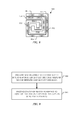
- FIG. 2 depicts a plan view of an example strain sensitive structure that is suitable for use in a display stack.
- the strain sensitive structure 200 can include a grid of independent optically transparent strain sensitive elements 204 that are formed in or on a substrate 202 .
- the strain sensitive elements 204 may be formed in or on at least a portion of one or both surfaces of the substrate 202 .
- the substrate 202 can be formed of any suitable material or materials.
- the substrate 202 is formed with an optically transparent material, such as polyethylene terephthalate (PET).
- PET polyethylene terephthalate
- the strain sensitive elements 204 are configured to detect strain based on an amount of force applied to an input region of the display.
- the strain sensitive elements 204 may be formed with a transparent conductive material or materials such as, for example, polyethyleneioxythiophene (PEDOT), a tin doped indium oxide (ITO) film, a gallium doped zinc oxide (GZO) film, an aluminum doped zinc oxide (AZO) film, carbon nanotubes, graphene, silver nanowire, other metallic nanowires, and the like.
- the strain sensitive elements 204 may be selected at least in part on temperature characteristics.
- the material selected for transparent strain sensitive elements 204 may have a negative temperature coefficient of resistance such that, as temperature increases, the electrical resistance decreases.
- the transparent strain sensitive elements 204 are formed as an array of rectilinear sensing elements, although other shapes and array patterns can also be used.
- each individual strain sensitive element 204 may have a selected shape and/or pattern.
- a strain sensitive element 204 may be deposited in a serpentine pattern, such as the pattern shown in FIG. 3 .
- a strain sensitive element 204 can have a different pattern or configuration in other embodiments.
- the strain sensitive element 204 may include at least two electrodes 300 , 302 that are configured to be physically or directly connected to one or more strain signal lines (not shown).
- the strain signal line(s) can be connected to a conductive contact 206 , which operably connects the strain sensitive element 204 to sense circuitry (not shown).
- the conductive contact 206 may be a continuous contact or can be formed in segments that surround or partially surround the array of strain sensitive elements 204 .
- a strain sensitive element 204 may be electrically connected to sense circuitry without the use of electrodes.
- a strain sensitive element 204 may be connected to the sense circuitry using conductive traces that are formed as part of a film layer.
- each strain sensitive element 204 is connected to the conductive contact 206 using strain signal lines 400 , 402 , respectively. Together the strain sensitive element 204 and the strain signal lines 400 , 402 physically or directly connected to the strain sensitive element 204 form a strain sensor 404 .
- a gauge factor and/or a conductance of the strain sensitive element 204 and/or the strain signal line(s) 400 , 402 can be based at least in part on the configuration of the strain sensitive structure 200 , on the operating conditions of the electronic device, and/or on the operating conditions of the component (e.g., display) in the electronic device that includes one or more strain sensors.
- FIG. 5 is a flowchart of a first method for producing a strain sensor.
- one or more strain sensitive elements are provided that have a material or combination of materials that have been formed or processed to have a first conductance and a first gauge factor (block 500 ).
- one or more strain signal lines that are directly connected to each strain sensitive element are provided, where the strain signal line(s) include a material or combination of materials that have been formed or processed to have a different second conductance and a different second gauge factor.
- FIGS. 6-11 Various embodiments of such strain sensitive elements and strain signal line(s) are described in more detail in conjunction with FIGS. 6-11 .
- the material(s) of each strain sensitive element has a lower conductance than the conductance of the material(s) of the at least one strain signal line.
- the material(s) of each strain sensitive element may have a higher electrical resistance than the material(s) of the at least one strain signal line.
- the first gauge factor of the strain sensitive element is higher than the second gauge factor of the at least one strain signal line that is connected to the strain sensitive element.
- the strain sensitive element is more sensitive to strain than the strain signal line(s) and the strain signal line(s) is configured to transmit signals more effectively.
- the strain sensitive element may be formed with a transparent GZO film or a transparent AZO film and the at least one strain signal line formed with a transparent ITO film.
- the strain sensitive structure 600 includes a strain sensitive element 204 disposed on a surface of the substrate 202 .
- the strain sensitive element 204 is connected to at least one strain signal line 400 .
- the strain sensitive element 204 is made of a material or combination of materials that has a first conductance and a first gauge factor and the at least one strain signal line 400 is made of a material or combination of materials having a different second conductance and a different second gauge factor.
- the at least one strain signal line 400 is connected to the conductive contact 206 .
- the conductive contact is made of copper and is positioned in a non-visible area of an electronic device (e.g., in a non-visible area of a display).
- a dielectric or insulating layer 602 may be disposed over at least a portion of the at least one strain signal line 400 and the strain sensitive element 204 .
- the insulating layer 602 may act as a protective layer for the strain signal line 400 and the strain sensitive element 204 .
- the insulating layer 602 can be made of a material or combination of materials that has an index of refraction that substantially matches the index of refraction of the strain sensitive element 204 and/or the at least one strain signal line 400 .
- FIG. 7 is a simplified cross-sectional view taken along line A-A in FIG. 4 of a second strain sensitive structure that is suitable for use as the strain sensitive structure 200 shown in FIG. 2 .
- the strain sensitive structure 700 is similar to the strain sensitive structure 600 shown in FIG. 6 , with the exception of the strain sensitive element 204 .
- the strain sensitive element 204 is an alternating multi-layer transparent conductive structure that includes a layer of insulating material 702 positioned between two layers of conductive material 704 .
- Each layer of conductive material 704 can be made of a material or combination of materials that has a first conductance and a first gauge factor.
- the multi-layer structure of the strain sensitive element 204 is configured to have an overall electrical resistance that is lower than the strain sensitive element 204 in FIG. 6 (e.g., a solid layer of conductive material) while still providing a higher gauge factor.
- each layer of transparent conductive material can be formed with a transparent GZO film or a transparent AZO film.
- the strain signal line 400 that is connected to the strain sensitive element 204 can be formed with a material or combination of materials that has a conductance and a gauge factor that are different from the overall conductance and the gauge factor of the multi-layer structure of the strain sensitive element 204 .
- the overall conductance of the strain sensitive element 204 may be less than the conductance of the strain signal line(s), while the gauge factor of the strain sensitive element 204 can be greater than the gauge factor of the strain signal line(s).
- the strain sensitive element has a higher gauge factor than the gauge factor of the at least one strain signal line connected to the strain sensitive element.
- the higher gauge factor allows the strain sensitive element to be more sensitive to strain than the strain signal line(s).
- the electrical conductance of the strain signal line(s) is higher than the conductance of the strain sensitive element. Due to the higher conductance, the strain signal line or lines efficiently transmit signals produced by the strain sensitive element to the conductive contact 206 .
- the strain sensitive element 800 is a hybrid strain sensitive element that is formed with two or more materials having different properties.
- one segment 802 in the hybrid strain sensitive element 800 is made of a first conductive material that has a first conductance and first gauge factor and another segment 804 is made of a second conductive material that has a different second conductance and a different second gauge factor, where the first conductance is greater than the second conductance and the second gauge factor is greater than the first gauge factor.
- the one or more strain signal lines that are directly connected to the hybrid strain sensitive element is formed or processed to have a gauge factor and a conductance that is different from the overall gauge factor and overall conductance of the strain sensitive element.
- the strain sensitive element has a greater overall gauge factor than the gauge factor of the at least one strain signal line.
- the higher overall gauge factor allows the strain sensitive element to be more sensitive to strain than the strain signal line(s).
- the electrical conductance of the strain signal line(s) is higher than the overall conductance of the strain sensitive element. Based on the higher conductance, the strain signal line(s) can effectively transmit signals produced by the strain sensitive element to the conductive contact 206 (see FIGS. 2 and 4 ).
- the segments 802 , 804 can have the same dimensions or one segment (e.g., segment 802 ) can have dimensions that are different from the dimensions of the other segment (e.g., segment 804 ).
- one segment can be longer than another segment, which may result in a given gauge factor and/or conductance.
- the given gauge factor can be a gauge factor that is equal to or greater than a threshold gauge factor.
- the given gauge factor and/or conductance can be based at least in part on the structure and/or operating conditions of the electronic device or a component in the electronic device that includes one or more hybrid strain sensors.
- at least two same segments e.g., at least two segments 802
- At least one segment 802 can have dimensions that differ from another segment 802 and/or at least one segment 804 can have dimensions that differ from another segment 804 . In another embodiment, all of the segments can have different dimensions. And in some embodiments, the hybrid strain sensitive element 800 may be formed with three or more materials having different properties.
- the embodiments of a strain sensor shown in FIGS. 6-8 are formed with two or more different materials.
- the materials are selected for a given gauge factor and/or an electrical conductance.
- Other embodiments can produce a strain sensor by processing either the strain sensitive elements and/or the one or more strain signal lines connected to the strain sensitive elements after the strain sensitive elements and the strain signal line(s) are formed.
- the material used to form the strain sensitive elements and the strain signal lines is the same material, and the strain sensitive elements and/or the strain signal lines are processed to adjust the conductance and/or the gauge factor of the processed component.
- the methods depicted in FIGS. 9 and 10 process the strain sensitive element and the strain signal line(s) respectively.
- FIG. 9 is a flowchart of a second method for producing a strain sensor.
- the strain sensitive element and the strain signal line(s) that is connected to the strain sensitive element are provided. Both the strain sensitive element and the strain signal line(s) are formed with one or more suitable materials. As described earlier, in some embodiments the strain sensitive element and the one or more strain signal lines are formed with the same material, such as, for example, a transparent conducting oxide film.
- the strain sensitive element is processed to increase the gauge factor of the strain sensitive element.
- the strain sensitive element may be processed using any suitable technique that increases the gauge factor of the strain sensitive element. For example, in one embodiment the strain sensitive element is laser annealed to increase the crystallinity of the strain sensitive element, which results in a higher gauge factor.
- FIG. 10 is a flowchart of a third method for producing a strain sensor.
- the strain sensitive element and the strain signal line(s) that is connected to the strain sensitive element are provided. Both the strain sensitive element and the strain signal line(s) are formed with one or more suitable materials. As described earlier, in some embodiments the strain sensitive element and the one or more strain signal lines are formed with the same material, such as, for example, a transparent conducting oxide film.
- the strain signal line(s) are processed to increase the conductance of the one or more strain signal lines.
- the strain signal line(s) may be processed using any suitable technique that increases the conductance of the strain signal line(s).
- the one or more strain signal lines are doped with a dopant or dopants that reduce the overall electrical resistance of the strain signal line(s), which in turn increases the conductance of the strain signal line(s).
- the one or more dopants can be diffused into the strain signal line(s) to increase the conductance of the strain signal line(s).
- one or more parameters of the fabrication process that is used to form the strain sensitive elements and/or the strain signal line(s) can be adjusted to increase the gauge factor and/or the conductance of the component.
- FIG. 11 is a flowchart of a fourth exemplar method for producing a strain sensor. Initially, one or more parameters of the process used to form a strain sensitive element on a substrate is adjusted to produce a strain sensitive element that has a higher gauge factor. For example, in one embodiment the flow rate of oxygen is increased when the strain sensitive element is deposited onto the substrate. The higher oxygen flow rate can reduce the carrier concentration and/or mobility of the carriers in the strain sensitive element.
- the thickness of the material used to form the strain sensitive element is adjusted to increase the gauge factor and/or to reduce the electrical resistance of the strain sensitive element.
- the material in a strain sensitive element can be formed as a thinner layer to result in a lower resistivity.
- one or more strain signal lines are formed on the substrate and connected to the strain sensitive element.
- One or more parameters of the fabrication process used to form the strain signal line(s) may be altered to increase the conductance of the strain signal line(s). Additionally or alternatively, the one or more strain signal lines can be processed after formation to increase the conductance of the strain signal line(s).
- a full sheet of a transparent conducting oxide film can be formed over and extend across the surface of a substrate (e.g., substrate 202 in FIG. 2 ) and select regions or areas of the film processed to produce the strain sensitive elements and/or the strain signal lines.
- a mask can be formed over a transparent conducting oxide film, where select areas of the mask that correspond to the locations of the strain sensitive elements are removed.
- the exposed select regions of the transparent conducting oxide film can then be doped to produce the strain sensitive elements in the full sheet of the transparent conducting oxide film.
- the dopant or dopants can be selected to produce strain sensitive elements that have a given gauge factor, or that have a gauge factor that is equal to or greater than a threshold gauge factor.
- select areas of a mask that correspond to the locations of the strain signal lines can be removed, and the exposed select regions of the transparent conducting oxide film can be doped to produce the strain signal lines in the full sheet of the transparent conducting oxide film.
- the dopant or dopants can be selected to produce strain signal lines that have a given conductance, or that have a conductance that is equal to or greater than a threshold conductance.
- two or more sheets of a transparent conducting oxide film can be formed over the surface of a substrate (e.g., substrate 202 in FIG. 2 ) and select regions or areas of the films processed to produce the strain sensitive elements and/or the strain signal lines.
- a substrate e.g., substrate 202 in FIG. 2
- select regions or areas of the films processed to produce the strain sensitive elements and/or the strain signal lines For example, one mask having openings that correspond to the locations of the strain sensitive elements can be formed over at least a portion of a transparent conducting oxide film. The exposed regions of the transparent conducting oxide film can then be doped to produce the strain sensitive elements in the full sheet of the transparent conducting oxide film.
- a second mask can be formed over at least a portion of a sheet of a conducting oxide film. The second mask can have openings at locations that correspond to the locations of the strain signal lines. The exposed select regions of the transparent conducting oxide film can be doped to produce the strain signal lines.
- FIG. 12 there is shown an illustrative block diagram of an electronic device that can include one or more strain sensors.
- one or more strain sensors can be located on a variety of components and/or at one or more different locations in an electronic device to detect a force applied on the component or on the electronic device.
- the illustrated electronic device 1200 can include one or more processing devices 1202 , memory 1204 , one or more input/output (I/O) devices 1206 , a power source 1208 , one or more sensors 1210 , a network communication interface 1212 , and a display 1214 , each of which will be discussed in more detail.
- I/O input/output
- the one or more processing devices 1202 can control some or all of the operations of the electronic device 1200 .
- the processing device(s) 1202 can communicate, either directly or indirectly, with substantially all of the components of the device.
- one or more system buses 1216 or other communication mechanisms can provide communication between the processing device(s) 1202 , the memory 1204 , the I/O device(s) 1206 , the power source 1208 , the one or more sensors 1210 , the network communication interface 1212 , and/or the display 1214 .
- At least one processing device can be configured to determine an amount of force and/or a change in force applied to an I/O device 1206 , the display, and/or the electronic device 1200 based on a signal received from one or more strain sensors.
- the processing device(s) 1202 can be implemented as any electronic device capable of processing, receiving, or transmitting data or instructions.
- the one or more processing devices 1202 can be a microprocessor, a central processing unit (CPU), an application-specific integrated circuit (ASIC), a digital signal processor (DSP), or combinations of multiple such devices.
- the term “processing device” is meant to encompass a single processor or processing unit, multiple processors, multiple processing units, or other suitably configured computing element or elements.
- the memory 1204 can store electronic data that can be used by the electronic device 1200 .
- the memory 1204 can store electrical data or content such as audio files, document files, timing and control signals, operational settings and data, and image data.
- the memory 1204 can be configured as any type of memory.
- memory 1204 can be implemented as random access memory, read-only memory, Flash memory, removable memory, or other types of storage elements, in any combination.
- the one or more I/O devices 1206 can transmit and/or receive data to and from a user or another electronic device.
- Example I/O device(s) 1206 include, but are not limited to, a touch sensing device such as a touchscreen or track pad, one or more buttons, a microphone, a haptic device, a speaker, and/or a force sensing device 1218 .
- the force sensing device 1218 can include one or more strain sensors.
- the strain sensor(s) can be configured as one of the strain sensors discussed earlier in conjunction with FIGS. 2-11 .
- the I/O device 106 shown in FIG. 1 may include a force sensing device 1218 .
- the force sensing device 1218 can include one or more strain sensors that are configured according to one of the embodiments shown in FIGS. 2-11 .
- An amount of force that is applied to the I/O device 106 , and/or a change in an amount of applied force can be determined based on the signal(s) received from the strain sensor(s).
- the power source 1208 can be implemented with any device capable of providing energy to the electronic device 1200 .
- the power source 1208 can be one or more batteries or rechargeable batteries, or a connection cable that connects the electronic device to another power source such as a wall outlet.
- the electronic device 1200 may also include one or more sensors 1210 positioned substantially anywhere on or in the electronic device 1200 .
- the sensor or sensors 1210 may be configured to sense substantially any type of characteristic, such as but not limited to, images, pressure, light, heat, touch, force, temperature, humidity, movement, relative motion, biometric data, and so on.
- the sensor(s) 1210 may be an image sensor, a temperature sensor, a light or optical sensor, an accelerometer, an environmental sensor, a gyroscope, a magnet, a health monitoring sensor, and so on.
- the one or more sensors 1210 can include a force sensing device that includes one or more strain sensors.
- the strain sensor(s) can be configured as one of the strain sensors discussed earlier in conjunction with FIGS. 2-11 .
- the electronic device shown in FIG. 1 may include a force sensing device 1220 in or under at least a portion of the enclosure 102 .
- the force sensing device 1220 can include one or more strain sensors that may be configured as one of the strain sensors discussed earlier in conjunction with FIGS. 2-11 .
- An amount of force that is applied to the enclosure 102 , and/or a change in an amount of applied force can be determined based on the signal(s) received from the strain sensor(s).
- the network communication interface 1212 can facilitate transmission of data to or from other electronic devices.
- a network communication interface can transmit electronic signals via a wireless and/or wired network connection.
- wireless and wired network connections include, but are not limited to, cellular, Wi-Fi, Bluetooth, infrared, RFID, Ethernet, and NFC.
- the display 1214 can provide a visual output to the user.
- the display 1214 can be implemented with any suitable technology, including, but not limited to, a multi-touch sensing touchscreen that uses liquid crystal display (LCD) technology, light emitting diode (LED) technology, organic light-emitting display (OLED) technology, organic electroluminescence (OEL) technology, or another type of display technology.
- the display 1214 can function as an input device that allows the user to interact with the electronic device 1200 .
- the display can include a touch sensing device 1222 .
- the touch sensing device 1222 can allow the display to function as a touch or multi-touch display.
- the display 1214 may include a force sensing device 1224 .
- the force sensing device 1224 is included in a display stack of the display 1214 .
- the force sensing device 1224 can include one or more strain sensors. An amount of force that is applied to the display 1214 , or to a cover glass disposed over the display, and/or a change in an amount of applied force can be determined based on the signal(s) received from the strain sensor(s).
- the strain sensor(s) can be configured as one of the strain sensors discussed earlier in conjunction with FIGS. 2-11 .
- FIG. 12 is exemplary only. In other examples, the electronic device may include fewer or more components than those shown in FIG. 12 . Additionally or alternatively, the electronic device can be included in a system and one or more components shown in FIG. 12 is separate from the electronic device but in communication with the electronic device. For example, an electronic device may be operatively connected to, or in communication with a separate display. As another example, one or more applications or data can be stored in a memory separate from the electronic device. In some embodiments, the separate memory can be in a cloud-based system or in an associated electronic device.
- FIG. 13 depicts a cross-sectional view of an example display stack that includes strain sensors.
- the display stack 1300 includes a cover glass 1301 positioned over a front polarizer 1302 .
- the cover glass 1301 can be a flexible touchable surface that is made of any suitable material, such as, for example, glass, plastic, sapphire, or combinations thereof.
- the cover glass 1301 can act as an input region for a touch sensing device and a force sensing device by receiving touch and force inputs from a user. The user can touch and/or apply force to the cover glass 1301 with one or more fingers or with another element such as a stylus.
- An adhesive layer 1304 can be disposed between the cover glass 1301 and the front polarizer 1302 . Any suitable adhesive can be used for the adhesive layer, such as, for example, an optically clear adhesive.
- a display layer 1306 can be positioned below the front polarizer 1302 . As described previously, the display layer 1306 may take a variety of forms, including a liquid crystal display (LCD), a light-emitting diode (LED) display, and an organic light-emitting diode (OLED) display. In some embodiments, the display layer 1306 can be formed from glass or have a glass substrate. Embodiments described herein include a multi-touch touchscreen LCD display layer.
- the display layer 1306 can include one or more layers.
- a display layer 1306 can include a VCOM buffer layer, a LCD display layer, and a conductive layer disposed over and/or under the display layer.
- the conductive layer may comprise an indium tin oxide (ITO) layer.
- a rear polarizer 1308 may be positioned below the display layer 1306 , and a strain sensitive structure 1310 below the rear polarizer 1308 .
- the strain sensitive structure 1310 includes a substrate 1312 having a first set of independent transparent strain sensors 1314 on a first surface 1316 of the substrate 1312 and a second set of independent transparent strain sensors 1318 on a second surface 1320 of the substrate 1312 .
- the first and second sets of transparent strain sensors are located in an area of the display stack that is visible to a user.
- a strain sensor includes a strain sensitive element and the one or more strain signal lines physically or directly connected to the strain sensitive element.
- the first and second surfaces 1316 , 1320 are opposing top and bottom surfaces of the substrate 1312 , respectively.
- An adhesive layer 1322 may attach the substrate 1312 to the rear polarizer 1308 .
- the strain sensors may be formed as an array of rectilinear strain sensors.
- Each strain sensitive element in the first set of independent strain sensors 1314 is aligned vertically with a respective one of the strain sensitive elements in the second set of independent strain sensors 1318 .
- each individual strain sensitive element may take a selected shape.
- the strain sensitive elements may be deposited in a serpentine pattern, similar to the serpentine pattern shown in FIG. 3 .
- a back light unit 1324 can be disposed below (e.g., attached to) the strain sensitive structure 1310 .
- the back light unit 1324 may be configured to support one or more portions of the substrate 1312 that do not include strain sensitive elements.
- the back light unit 1324 can support the ends of the substrate 1312 .
- Other embodiments may configure a back light unit differently.
- the strain sensors are typically connected to sense circuitry 1326 through conductive connectors 1328 .
- the sense circuitry 1326 is configured to detect changes in an electrical property of each of the strain sensitive elements.
- the sense circuitry 1326 may be configured to detect changes in the electrical resistance of the strain sensitive elements, which can be correlated to a force that is applied to the cover glass 1301 .
- the sense circuitry 1326 may also be configured to provide information about the location of a touch based on the relative difference in the change of electrical resistance of the strain sensors 1314 , 1318 .
- the strain sensitive elements are formed with a transparent conducting oxide film.
- an input region e.g., the cover glass 1301
- the planar strain sensitive structure 1310 is strained and the electrical resistance of the transparent conducting oxide film changes in proportion to the strain.
- the force can cause the strain sensitive structure 1310 to bend slightly.
- the bottom surface 1400 of the strain sensitive structure 1310 elongates while the top surface 1402 compresses.
- the strain sensitive elements measure the elongation or compression of the surface, and these measurements can be correlated to the amount of force applied to the input region.
- the sense circuitry 1326 may be adapted to receive signals from each strain sensing device 1334 and determine a difference in an electrical property of each strain sensing device. For example, as described above, a force may be received at the cover glass 1301 , which in turn causes the strain sensitive structure 1310 to bend.
- the sense circuitry 1326 is configured to detect changes in an electrical property (e.g., electrical resistance) of the one or more strain sensing devices based on signals received from the strain sensing device(s) 1334 , and these changes are correlated to the amount of force applied to the cover glass 1301 .
- a gap 1336 exists between the strain sensitive structure 1310 and the back light unit 1324 .
- Strain measurements intrinsically measure the force at a point on the top surface 1316 of the substrate 1312 plus the force from the bottom at that point on the bottom surface 1320 of the substrate 1312 .
- the gap 1336 is present, there are no forces on the bottom surface 1320 .
- the forces on the top surface 1316 can be measured independently of the forces on the bottom surface 1320 .
- the strain sensitive structure 1310 may be positioned above the display layer when the display stack 1300 does not include the gap 1336 .
- a strain sensitive structure can include only one set of strain sensitive elements on a surface of the substrate.
- a processing device may be configured to determine an amount of force, or a change in force, applied to an input region based on signals received from the set of strain sensitive elements.
- the strain sensing device 1334 (see FIG. 13 ) that includes two-vertically aligned strain sensitive elements can be modeled as two resistors R SENSE configured as a voltage divider.
- a reference voltage divider 1502 includes two reference resistors R REF .
- the strain sensing device 1334 and the reference voltage divider 1502 may be modeled as a Wheatstone bridge circuit, with the strain sensing device 1334 forming one half bridge of the Wheatstone bridge circuit and the reference voltage divider 1502 forming the other half bridge of the Wheatstone bridge circuit.
- Other embodiments can model the strain sensor and the reference resistors differently.
- a strain sensitive structure may include only one set of strain sensitive elements and a particular strain sensitive element and a reference resistor can be modeled as a Wheatstone half bridge circuit.
- a first reference voltage (V REF _ TOP ) is received at node 1504 and a second reference voltage (V REF _ BOT ) is received at node 1506 .
- a force signal at node 1508 of the strain sensing device 1334 and a reference signal at node 1510 of the reference voltage divider 1502 are received by the sense circuitry 1512 .
- the sense circuitry 1512 is configured to detect changes in an electrical property (e.g., electrical resistance) of the strain sensing device 1334 based on the differences in the force and reference signals of the two voltage dividers. The changes can be correlated to the amount of force applied to a respective input region of an electronic device (e.g., the cover glass 1201 in FIG. 12 ).
- the one or more strain sensitive elements can be formed with a non-metal opaque material. Additionally or alternatively, the one or more strain sensitive elements can be formed on one layer and the strain signal line(s) on another layer such that a strain sensitive element and corresponding strain signal line(s) are not co-planar (on different planar surfaces).
- a via can be formed through the interposing layer or layers to produce an electrical contact between the strain sensitive element and the strain signal lines.
Landscapes
- Engineering & Computer Science (AREA)
- Physics & Mathematics (AREA)
- General Physics & Mathematics (AREA)
- General Engineering & Computer Science (AREA)
- Theoretical Computer Science (AREA)
- Human Computer Interaction (AREA)
- Measurement Of Length, Angles, Or The Like Using Electric Or Magnetic Means (AREA)
- Measurement Of Force In General (AREA)
- Devices For Indicating Variable Information By Combining Individual Elements (AREA)
Abstract
One or more strain sensors can be included in an electronic device. Each strain sensor includes a strain sensitive element and one or more strain signal lines connected directly to the strain sensitive element. The strain sensor(s) are used to detect a force that is applied to the electronic device, to a component in the electronic device, and/or to an input region or surface of the electronic device. A strain sensitive element is formed or processed to have a first gauge factor and the strain signal line(s) is formed or processed to have a different second gauge factor. Additionally or alternatively, a strain sensitive element is formed or processed to have a first conductance and the strain signal line(s) is formed or processed to have a different second conductance.
Description
This application is a continuation of U.S. patent application Ser. No. 14/823,910, filed Aug. 11, 2015, and entitled “Transparent Strain Sensors in an Electronic Device,” which claims the benefit under 35 U.S.C. § 119(e) of U.S. Provisional Patent Application No. 62/195,030, filed on Jul. 21, 2015, and entitled “Transparent Strain Sensors in an Electronic Device,” both of which are incorporated by reference as if fully disclosed herein.
Embodiments described herein generally relate to electronic devices. More particularly, the present embodiments relate to one or more transparent strain sensors in an electronic device.
Strain gauges or sensors are used to detect or measure strain on an object. Typically, the electrical resistance of a strain sensor varies in proportion to the compression and tension forces it is experiencing. The gauge factor of a strain sensor represents the sensitivity of the material to strain. In other words, the gauge factor indicates how much the resistance of the strain sensor changes with strain. The higher the gauge factor, the larger the change in resistance. Higher gauge factors allow a greater range of strain to be detected and measured.
In some situations, it is desirable for the strain sensors to be made of a transparent material. For example, transparent strain sensors may be used when the strain sensors are located in an area where the strain sensors can be detected visually by a user (e.g., though a display). However, some materials that are used to form transparent strain sensors have low or zero gauge factors.
One or more transparent strain sensors can be included in an electronic device. As used herein, the term “strain sensor” refers to a strain sensitive element and the one or more strain signal lines that connect directly to the strain sensitive element. In one embodiment, the strain sensor(s) are used to detect a force that is applied to the electronic device, to a component in the electronic device, such as an input button, and/or to an input region or surface of the electronic device. In one non-limiting example, a force sensing device that includes one or more strain sensors may be incorporated into a display stack of an electronic device. The one or more strain sensors can be positioned in an area of the display stack that is visible to a user when the user is viewing the display. As such, the one or more transparent strain sensors can be formed with a transparent conductive material or two or more transparent conductive materials.
In some embodiments, each transparent strain sensitive element is formed or processed to have a first gauge factor and a first conductance. Each transparent strain signal line is formed or processed to have a different second gauge factor and a different first conductance. For example, in one embodiment the transparent material or materials that form a transparent strain sensitive element may have a higher gauge factor than the transparent material(s) of the at least one transparent strain signal line while the conductance of the transparent strain sensitive element may be less than the conductance of the transparent strain signal line(s). Thus, the transparent strain sensitive element is configured to be more sensitive to strain than the transparent strain signal line(s) and the transparent strain signal line(s) is configured to transmit signals more effectively.
In one aspect a transparent strain sensor includes a transparent strain sensitive element and a transparent strain signal line connected directly to the strain sensitive element. The transparent strain sensitive element is formed with comprised a first transparent conductive material having a first gauge factor. The transparent strain signal line is formed with a second transparent conductive material having a second gauge factor. The first gauge factor can be greater than the second gauge factor in one embodiment. Additionally or alternatively, the first transparent conductive material may have a first electrical resistance and the second transparent conductive material a second electrical resistance with the first electrical resistance being greater than the second electrical resistance. In a non-limiting example, the transparent strain sensitive element may be formed with a transparent GZO film or a transparent AZO film and the at least one transparent strain signal line is formed with a transparent ITO film.
In another aspect, a transparent strain sensor can be formed with a hybrid transparent conductive material that includes at least one first transparent conductive segment that has a first gauge factor and a first electrical resistance and at least one second transparent conductive segment that has a second gauge factor and a second electrical resistance. The first transparent conductive segment is connected to the second transparent conductive segment. The first gauge factor can be greater than the second gauge factor and the first electrical resistance greater than the second electrical resistance.
In another aspect, a transparent strain sensor can include a transparent strain sensitive element and at least one transparent strain signal line connected directly to the transparent strain sensitive element. The transparent strain sensitive element and transparent strain signal line(s) can be formed with the same a transparent conductive material or materials, but the transparent conductive material(s) in the strain sensitive element and/or in the at least one strain signal line may be doped with one or more dopants to change the gauge factor and/or the conductance of the transparent conductive material. Thus, the transparent strain sensitive element and the at least one transparent strain signal line can have different gauge factors and/or electrical conductance. In some embodiments, the gauge factor of the transparent strain sensitive element is greater than the gauge factor of the at least one strain signal line. Additionally or alternatively, the transparent strain sensitive element can have a first electrical resistance and the transparent strain signal line(s) a second overall electrical resistance where the first electrical resistance is greater than the second electrical resistance.
In yet another aspect, a method for producing a transparent strain sensor may include providing a transparent strain sensitive element on a substrate and providing a transparent strain signal line that is connected directly to the transparent strain sensitive element on the substrate. The transparent strain sensitive element is formed with one or more transparent conductive materials having a first gauge factor. The transparent strain signal line is formed with one or more transparent conductive materials having a different second gauge factor.
In another aspect, a method for producing a transparent strain sensor can include providing a transparent strain sensitive element on a substrate, where the transparent strain sensitive element comprises one or more transparent conductive materials, and providing a transparent strain signal line that is connected directly to the strain sensitive element on the substrate. The one or more transparent conductive materials of the transparent strain sensitive element is processed to increase a gauge factor of the transparent strain sensitive element. In one non-limiting example, the one or more transparent conductive materials may be can be laser annealed to increase the crystallinity of the transparent strain sensitive element, which results in a higher gauge factor. In some embodiments, the transparent strain signal line can also be formed with the same or different transparent conductive material(s), and the transparent conductive material(s) of the transparent strain signal line may be processed to increase a conductance of the transparent strain signal line.
In yet another aspect, a method for producing a transparent strain sensor may include providing a transparent strain sensitive element on a substrate and providing a transparent strain signal line that is connected directly to the strain sensitive element on the substrate. The transparent strain signal line is formed with one or more transparent conductive materials. The one or more transparent conductive materials of the transparent strain signal line can be processed to increase a conductance of the transparent strain signal line. In one non-limiting example, the one or more transparent conductive materials may be doped with a dopant or dopants that reduce the overall electrical resistance of the strain signal line, which in turn increases the conductance of the transparent strain signal line.
In yet another aspect, an electronic device can include a cover glass and a strain sensing structure positioned below the cover glass. The strain sensing structure may include a substrate, a first transparent strain sensitive element positioned on a first surface of the substrate and a second transparent strain sensitive element positioned on a second surface of the substrate. One or more transparent strain signal lines are connected to each transparent strain sensitive element. In some embodiments, the first and second transparent strain sensitive elements have a gauge factor that is greater than a gauge factor of the transparent strain signal lines. Sense circuitry is electrically connected to the transparent strain signal lines, and a controller is operably connected to the sense circuitry. The controller is configured to determine an amount of force applied to the cover glass based on the signals received from the sense circuitry. In some embodiments, the first and second transparent strain sensitive elements and the transparent strain signal lines are positioned in an area of the display stack that is visible to a user when the user is viewing the display.
The disclosure will be readily understood by the following detailed description in conjunction with the accompanying drawings, wherein like reference numerals designate like structural elements, and in which:
Reference will now be made in detail to representative embodiments illustrated in the accompanying drawings. It should be understood that the following descriptions are not intended to limit the embodiments to one preferred embodiment. To the contrary, it is intended to cover alternatives, modifications, and equivalents as can be included within the spirit and scope of the described embodiments as defined by the appended claims.
The following disclosure relates to an electronic device that includes one or more strain sensors configured to detect strain based on an amount of force applied to the electronic device, a component in the electronic device, and/or an input region of the electronic device. As one example, the one or more strain sensors can be incorporated into a display stack of an electronic device, and at least a portion of the top surface of the display screen may be an input region. In some embodiments, the one or more transparent strain sensors are located in an area of the display stack that is visible to a user when the user is viewing the display. As used herein, the term “strain sensor” includes a strain sensitive element and at least one strain signal line physically or directly connected to the strain sensitive element. Additionally, “optically transparent” and “transparent” are defined broadly to include a material that is transparent, translucent, or not visibly discernable by the human eye.
In some embodiments, each strain sensitive element is formed or processed to have a first gauge factor and a first conductance. Each strain signal line is formed or processed to have a different second gauge factor and a different first conductance. For example, in one embodiment the material or materials that form a strain sensitive element may have a higher gauge factor than the material(s) of the at least one strain signal line while the conductance of the strain sensitive element may be less than the conductance of the strain signal line(s). Thus, the strain sensitive element is configured to be more sensitive to strain than the strain signal line(s) and the strain signal line(s) is configured to transmit signals more effectively. In a non-limiting example, the strain sensitive element may be formed with a transparent GZO film or a transparent AZO film and the at least one strain signal line formed with a transparent ITO film.
In some embodiments, a gauge factor and/or a conductance of a strain sensitive element or a strain signal line can be based at least in part on the structure and/or the operating conditions of the electronic device or a component in the electronic device that includes one or more strain sensors.
In another embodiment, a strain sensitive element and/or the one or more strain signal lines connected to the strain sensitive element may be processed after the strain sensitive elements and the strain signal line(s) are formed. In a non-limiting example, the material used to form the strain sensitive element and the strain signal line(s) can be the same material or materials, and the material(s) in the strain sensitive element and/or the material(s) in the strain signal lines is processed to adjust the conductance and/or the gauge factor of the processed component. In one embodiment, the strain sensitive element can be laser annealed to increase the crystallinity of the strain sensitive element, which results in a higher gauge factor. Additionally or alternatively, the one or more strain signal lines may be doped with a dopant or dopants that reduce the overall electrical resistance of the strain signal line(s), which in turn increases the conductance of the strain signal line(s).
And in yet another embodiment, one or more parameters of the fabrication process that is used to form the strain sensitive element and/or the strain signal line(s) may be adjusted to increase the gauge factor and/or the conductance of the component. For example, in one embodiment the flow rate of oxygen can be increased when the strain sensitive element is deposited onto the substrate. The higher oxygen flow rate can reduce the carrier concentration and/or mobility of the carriers in the strain sensitive element. In another embodiment, the thickness of the material used to form the strain sensitive element and/or the strain signal line(s) may be adjusted to increase the gauge factor or the conductance of the component.
Directional terminology, such as “top”, “bottom”, “front”, “back”, “leading”, “trailing”, etc., is used with reference to the orientation of the Figure(s) being described. Because components of embodiments described herein can be positioned in a number of different orientations, the directional terminology is used for purposes of illustration only and is in no way limiting. When used in conjunction with layers of a display or device, the directional terminology is intended to be construed broadly, and therefore should not be interpreted to preclude the presence of one or more intervening layers or other intervening features or elements. Thus, a given layer that is described as being formed, positioned, disposed on or over another layer, or that is described as being formed, positioned, disposed below or under another layer may be separated from the latter layer by one or more additional layers or elements.
These and other embodiments are discussed below with reference to FIGS. 1-15 . However, those skilled in the art will readily appreciate that the detailed description given herein with respect to these Figures is for explanatory purposes only and should not be construed as limiting.
The electronic device 100 includes an enclosure 102 surrounding a display 104 and one or more input/output (I/O) devices 106 (shown as button). The enclosure 102 can form an outer surface or partial outer surface for the internal components of the electronic device 100, and may at least partially surround the display 104. The enclosure 102 can be formed of one or more components operably connected together, such as a front piece and a back piece. Alternatively, the enclosure 102 can be formed of a single piece operably connected to the display 104.
The display 104 can be implemented with any suitable display, including, but not limited to, a multi-touch sensing touchscreen device that uses liquid crystal display (LCD) technology, light emitting diode (LED) technology, organic light-emitting display (OLED) technology, or organic electro luminescence (OEL) technology.
In some embodiments, the I/O device 106 can take the form of a home button, which may be a mechanical button, a soft button (e.g., a button that does not physically move but still accepts inputs), an icon or image on a display, and so on. Further, in some embodiments, the button can be integrated as part of a cover glass of the electronic device. Although not shown in FIG. 1 , the electronic device 100 can include other types of I/O devices, such as a microphone, a speaker, a camera, and one or more ports such as a network communication port and/or a power cord port.
Strain sensors can be included in one or more locations of the electronic device 100. For example, in one embodiment one or more strains sensors may be included in the I/O device 106. The strain sensor(s) can be used to measure an amount of force and/or a change in force that is applied to the I/O device 106. In another embodiment, one or more strain sensors can be positioned under at least a portion of the enclosure to detect a force and/or a change in force that is applied to the enclosure. Additionally or alternatively, one or more strains sensors may be included in a display stack for the display 104. The strain sensor(s) can be used to measure an amount of force and/or a change in force that is applied to the display or to a portion of the display. As described earlier, a strain sensor includes a strain sensitive element and at least one strain signal line physically or directly connected to the strain sensitive element.
In one non-limiting example, the entire top surface of a display may be an input region that is configured to receive one or more force inputs from a user. FIG. 2 depicts a plan view of an example strain sensitive structure that is suitable for use in a display stack. The strain sensitive structure 200 can include a grid of independent optically transparent strain sensitive elements 204 that are formed in or on a substrate 202. The strain sensitive elements 204 may be formed in or on at least a portion of one or both surfaces of the substrate 202. The substrate 202 can be formed of any suitable material or materials. In one embodiment, the substrate 202 is formed with an optically transparent material, such as polyethylene terephthalate (PET).
As discussed earlier, the strain sensitive elements 204 are configured to detect strain based on an amount of force applied to an input region of the display. The strain sensitive elements 204 may be formed with a transparent conductive material or materials such as, for example, polyethyleneioxythiophene (PEDOT), a tin doped indium oxide (ITO) film, a gallium doped zinc oxide (GZO) film, an aluminum doped zinc oxide (AZO) film, carbon nanotubes, graphene, silver nanowire, other metallic nanowires, and the like. In certain embodiments, the strain sensitive elements 204 may be selected at least in part on temperature characteristics. For example, the material selected for transparent strain sensitive elements 204 may have a negative temperature coefficient of resistance such that, as temperature increases, the electrical resistance decreases.
In this example, the transparent strain sensitive elements 204 are formed as an array of rectilinear sensing elements, although other shapes and array patterns can also be used. In many examples, each individual strain sensitive element 204 may have a selected shape and/or pattern. For example, in certain embodiments, a strain sensitive element 204 may be deposited in a serpentine pattern, such as the pattern shown in FIG. 3 . A strain sensitive element 204 can have a different pattern or configuration in other embodiments.
The strain sensitive element 204 may include at least two electrodes 300, 302 that are configured to be physically or directly connected to one or more strain signal lines (not shown). The strain signal line(s) can be connected to a conductive contact 206, which operably connects the strain sensitive element 204 to sense circuitry (not shown). The conductive contact 206 may be a continuous contact or can be formed in segments that surround or partially surround the array of strain sensitive elements 204. In other embodiments, a strain sensitive element 204 may be electrically connected to sense circuitry without the use of electrodes. For example, a strain sensitive element 204 may be connected to the sense circuitry using conductive traces that are formed as part of a film layer.
Referring now to FIG. 4 , there is shown an enlarged view of the area 208 shown in FIG. 2 . The electrodes 300, 302 of each strain sensitive element 204 are connected to the conductive contact 206 using strain signal lines 400, 402, respectively. Together the strain sensitive element 204 and the strain signal lines 400, 402 physically or directly connected to the strain sensitive element 204 form a strain sensor 404. In some embodiments, a gauge factor and/or a conductance of the strain sensitive element 204 and/or the strain signal line(s) 400, 402 can be based at least in part on the configuration of the strain sensitive structure 200, on the operating conditions of the electronic device, and/or on the operating conditions of the component (e.g., display) in the electronic device that includes one or more strain sensors.
In one embodiment, the material(s) of each strain sensitive element has a lower conductance than the conductance of the material(s) of the at least one strain signal line. For example, the material(s) of each strain sensitive element may have a higher electrical resistance than the material(s) of the at least one strain signal line. Additionally, the first gauge factor of the strain sensitive element is higher than the second gauge factor of the at least one strain signal line that is connected to the strain sensitive element. Thus, the strain sensitive element is more sensitive to strain than the strain signal line(s) and the strain signal line(s) is configured to transmit signals more effectively. In a non-limiting example, the strain sensitive element may be formed with a transparent GZO film or a transparent AZO film and the at least one strain signal line formed with a transparent ITO film.
Referring now to FIG. 6 , there is shown a simplified cross-sectional view taken along line A-A in FIG. 4 of a first strain sensitive structure that is suitable for use as the strain sensitive structure 200 shown in FIG. 2 . The strain sensitive structure 600 includes a strain sensitive element 204 disposed on a surface of the substrate 202. The strain sensitive element 204 is connected to at least one strain signal line 400. As described earlier, the strain sensitive element 204 is made of a material or combination of materials that has a first conductance and a first gauge factor and the at least one strain signal line 400 is made of a material or combination of materials having a different second conductance and a different second gauge factor.
The at least one strain signal line 400 is connected to the conductive contact 206. In some embodiments, the conductive contact is made of copper and is positioned in a non-visible area of an electronic device (e.g., in a non-visible area of a display). A dielectric or insulating layer 602 may be disposed over at least a portion of the at least one strain signal line 400 and the strain sensitive element 204. The insulating layer 602 may act as a protective layer for the strain signal line 400 and the strain sensitive element 204. In embodiments where the strain sensitive element and the strain signal line(s) are formed with a substantially transparent material or materials, the insulating layer 602 can be made of a material or combination of materials that has an index of refraction that substantially matches the index of refraction of the strain sensitive element 204 and/or the at least one strain signal line 400.
The strain signal line 400 that is connected to the strain sensitive element 204 can be formed with a material or combination of materials that has a conductance and a gauge factor that are different from the overall conductance and the gauge factor of the multi-layer structure of the strain sensitive element 204. As described earlier, the overall conductance of the strain sensitive element 204 may be less than the conductance of the strain signal line(s), while the gauge factor of the strain sensitive element 204 can be greater than the gauge factor of the strain signal line(s).
In the embodiments illustrated in FIGS. 6 and 7 , the strain sensitive element has a higher gauge factor than the gauge factor of the at least one strain signal line connected to the strain sensitive element. The higher gauge factor allows the strain sensitive element to be more sensitive to strain than the strain signal line(s). Additionally, in some embodiments the electrical conductance of the strain signal line(s) is higher than the conductance of the strain sensitive element. Due to the higher conductance, the strain signal line or lines efficiently transmit signals produced by the strain sensitive element to the conductive contact 206.
Referring now to FIG. 8 , there is shown a plan view of a third example of a strain sensitive element that is suitable for use as the strain sensitive element 204 shown in FIGS. 2 and 4 . The strain sensitive element 800 is a hybrid strain sensitive element that is formed with two or more materials having different properties. In the illustrated embodiment, one segment 802 in the hybrid strain sensitive element 800 is made of a first conductive material that has a first conductance and first gauge factor and another segment 804 is made of a second conductive material that has a different second conductance and a different second gauge factor, where the first conductance is greater than the second conductance and the second gauge factor is greater than the first gauge factor.
The one or more strain signal lines that are directly connected to the hybrid strain sensitive element is formed or processed to have a gauge factor and a conductance that is different from the overall gauge factor and overall conductance of the strain sensitive element. For example, the strain sensitive element has a greater overall gauge factor than the gauge factor of the at least one strain signal line. The higher overall gauge factor allows the strain sensitive element to be more sensitive to strain than the strain signal line(s). Additionally, in some embodiments the electrical conductance of the strain signal line(s) is higher than the overall conductance of the strain sensitive element. Based on the higher conductance, the strain signal line(s) can effectively transmit signals produced by the strain sensitive element to the conductive contact 206 (see FIGS. 2 and 4 ).
The segments 802, 804 can have the same dimensions or one segment (e.g., segment 802) can have dimensions that are different from the dimensions of the other segment (e.g., segment 804). For example, one segment can be longer than another segment, which may result in a given gauge factor and/or conductance. In some embodiments, the given gauge factor can be a gauge factor that is equal to or greater than a threshold gauge factor. The given gauge factor and/or conductance can be based at least in part on the structure and/or operating conditions of the electronic device or a component in the electronic device that includes one or more hybrid strain sensors. In one embodiment, at least two same segments (e.g., at least two segments 802) can have different dimensions. Thus, at least one segment 802 can have dimensions that differ from another segment 802 and/or at least one segment 804 can have dimensions that differ from another segment 804. In another embodiment, all of the segments can have different dimensions. And in some embodiments, the hybrid strain sensitive element 800 may be formed with three or more materials having different properties.
The embodiments of a strain sensor shown in FIGS. 6-8 are formed with two or more different materials. The materials are selected for a given gauge factor and/or an electrical conductance. Other embodiments can produce a strain sensor by processing either the strain sensitive elements and/or the one or more strain signal lines connected to the strain sensitive elements after the strain sensitive elements and the strain signal line(s) are formed. For example, in some embodiments the material used to form the strain sensitive elements and the strain signal lines is the same material, and the strain sensitive elements and/or the strain signal lines are processed to adjust the conductance and/or the gauge factor of the processed component. The methods depicted in FIGS. 9 and 10 process the strain sensitive element and the strain signal line(s) respectively.
Next, as shown in block 1000, the strain signal line(s) are processed to increase the conductance of the one or more strain signal lines. The strain signal line(s) may be processed using any suitable technique that increases the conductance of the strain signal line(s). For example, in one embodiment the one or more strain signal lines are doped with a dopant or dopants that reduce the overall electrical resistance of the strain signal line(s), which in turn increases the conductance of the strain signal line(s). For example, the one or more dopants can be diffused into the strain signal line(s) to increase the conductance of the strain signal line(s).
In still other embodiments, one or more parameters of the fabrication process that is used to form the strain sensitive elements and/or the strain signal line(s) can be adjusted to increase the gauge factor and/or the conductance of the component. FIG. 11 is a flowchart of a fourth exemplar method for producing a strain sensor. Initially, one or more parameters of the process used to form a strain sensitive element on a substrate is adjusted to produce a strain sensitive element that has a higher gauge factor. For example, in one embodiment the flow rate of oxygen is increased when the strain sensitive element is deposited onto the substrate. The higher oxygen flow rate can reduce the carrier concentration and/or mobility of the carriers in the strain sensitive element. In another embodiment, the thickness of the material used to form the strain sensitive element is adjusted to increase the gauge factor and/or to reduce the electrical resistance of the strain sensitive element. For example, the material in a strain sensitive element can be formed as a thinner layer to result in a lower resistivity.
Next, as shown in block 1102, one or more strain signal lines are formed on the substrate and connected to the strain sensitive element. One or more parameters of the fabrication process used to form the strain signal line(s) may be altered to increase the conductance of the strain signal line(s). Additionally or alternatively, the one or more strain signal lines can be processed after formation to increase the conductance of the strain signal line(s).
In some embodiments, a full sheet of a transparent conducting oxide film can be formed over and extend across the surface of a substrate (e.g., substrate 202 in FIG. 2 ) and select regions or areas of the film processed to produce the strain sensitive elements and/or the strain signal lines. For example, a mask can be formed over a transparent conducting oxide film, where select areas of the mask that correspond to the locations of the strain sensitive elements are removed. The exposed select regions of the transparent conducting oxide film can then be doped to produce the strain sensitive elements in the full sheet of the transparent conducting oxide film. The dopant or dopants can be selected to produce strain sensitive elements that have a given gauge factor, or that have a gauge factor that is equal to or greater than a threshold gauge factor. Similarly, select areas of a mask that correspond to the locations of the strain signal lines can be removed, and the exposed select regions of the transparent conducting oxide film can be doped to produce the strain signal lines in the full sheet of the transparent conducting oxide film. The dopant or dopants can be selected to produce strain signal lines that have a given conductance, or that have a conductance that is equal to or greater than a threshold conductance.
In other embodiments, two or more sheets of a transparent conducting oxide film can be formed over the surface of a substrate (e.g., substrate 202 in FIG. 2 ) and select regions or areas of the films processed to produce the strain sensitive elements and/or the strain signal lines. For example, one mask having openings that correspond to the locations of the strain sensitive elements can be formed over at least a portion of a transparent conducting oxide film. The exposed regions of the transparent conducting oxide film can then be doped to produce the strain sensitive elements in the full sheet of the transparent conducting oxide film. A second mask can be formed over at least a portion of a sheet of a conducting oxide film. The second mask can have openings at locations that correspond to the locations of the strain signal lines. The exposed select regions of the transparent conducting oxide film can be doped to produce the strain signal lines.
Referring now to FIG. 12 , there is shown an illustrative block diagram of an electronic device that can include one or more strain sensors. As discussed earlier, one or more strain sensors can be located on a variety of components and/or at one or more different locations in an electronic device to detect a force applied on the component or on the electronic device. The illustrated electronic device 1200 can include one or more processing devices 1202, memory 1204, one or more input/output (I/O) devices 1206, a power source 1208, one or more sensors 1210, a network communication interface 1212, and a display 1214, each of which will be discussed in more detail.
The one or more processing devices 1202 can control some or all of the operations of the electronic device 1200. The processing device(s) 1202 can communicate, either directly or indirectly, with substantially all of the components of the device. For example, one or more system buses 1216 or other communication mechanisms can provide communication between the processing device(s) 1202, the memory 1204, the I/O device(s) 1206, the power source 1208, the one or more sensors 1210, the network communication interface 1212, and/or the display 1214. At least one processing device can be configured to determine an amount of force and/or a change in force applied to an I/O device 1206, the display, and/or the electronic device 1200 based on a signal received from one or more strain sensors.
The processing device(s) 1202 can be implemented as any electronic device capable of processing, receiving, or transmitting data or instructions. For example, the one or more processing devices 1202 can be a microprocessor, a central processing unit (CPU), an application-specific integrated circuit (ASIC), a digital signal processor (DSP), or combinations of multiple such devices. As described herein, the term “processing device” is meant to encompass a single processor or processing unit, multiple processors, multiple processing units, or other suitably configured computing element or elements.
The memory 1204 can store electronic data that can be used by the electronic device 1200. For example, the memory 1204 can store electrical data or content such as audio files, document files, timing and control signals, operational settings and data, and image data. The memory 1204 can be configured as any type of memory. By way of example only, memory 1204 can be implemented as random access memory, read-only memory, Flash memory, removable memory, or other types of storage elements, in any combination.
The one or more I/O devices 1206 can transmit and/or receive data to and from a user or another electronic device. Example I/O device(s) 1206 include, but are not limited to, a touch sensing device such as a touchscreen or track pad, one or more buttons, a microphone, a haptic device, a speaker, and/or a force sensing device 1218. The force sensing device 1218 can include one or more strain sensors. The strain sensor(s) can be configured as one of the strain sensors discussed earlier in conjunction with FIGS. 2-11 .
As one example, the I/O device 106 shown in FIG. 1 may include a force sensing device 1218. As described earlier, the force sensing device 1218 can include one or more strain sensors that are configured according to one of the embodiments shown in FIGS. 2-11 . An amount of force that is applied to the I/O device 106, and/or a change in an amount of applied force can be determined based on the signal(s) received from the strain sensor(s).
The power source 1208 can be implemented with any device capable of providing energy to the electronic device 1200. For example, the power source 1208 can be one or more batteries or rechargeable batteries, or a connection cable that connects the electronic device to another power source such as a wall outlet.
The electronic device 1200 may also include one or more sensors 1210 positioned substantially anywhere on or in the electronic device 1200. The sensor or sensors 1210 may be configured to sense substantially any type of characteristic, such as but not limited to, images, pressure, light, heat, touch, force, temperature, humidity, movement, relative motion, biometric data, and so on. For example, the sensor(s) 1210 may be an image sensor, a temperature sensor, a light or optical sensor, an accelerometer, an environmental sensor, a gyroscope, a magnet, a health monitoring sensor, and so on. In some embodiments, the one or more sensors 1210 can include a force sensing device that includes one or more strain sensors. The strain sensor(s) can be configured as one of the strain sensors discussed earlier in conjunction with FIGS. 2-11 .
As one example, the electronic device shown in FIG. 1 may include a force sensing device 1220 in or under at least a portion of the enclosure 102. The force sensing device 1220 can include one or more strain sensors that may be configured as one of the strain sensors discussed earlier in conjunction with FIGS. 2-11 . An amount of force that is applied to the enclosure 102, and/or a change in an amount of applied force can be determined based on the signal(s) received from the strain sensor(s).
The network communication interface 1212 can facilitate transmission of data to or from other electronic devices. For example, a network communication interface can transmit electronic signals via a wireless and/or wired network connection. Examples of wireless and wired network connections include, but are not limited to, cellular, Wi-Fi, Bluetooth, infrared, RFID, Ethernet, and NFC.
The display 1214 can provide a visual output to the user. The display 1214 can be implemented with any suitable technology, including, but not limited to, a multi-touch sensing touchscreen that uses liquid crystal display (LCD) technology, light emitting diode (LED) technology, organic light-emitting display (OLED) technology, organic electroluminescence (OEL) technology, or another type of display technology. In some embodiments, the display 1214 can function as an input device that allows the user to interact with the electronic device 1200. For example, the display can include a touch sensing device 1222. The touch sensing device 1222 can allow the display to function as a touch or multi-touch display.
Additionally or alternatively, the display 1214 may include a force sensing device 1224. In some embodiments, the force sensing device 1224 is included in a display stack of the display 1214. The force sensing device 1224 can include one or more strain sensors. An amount of force that is applied to the display 1214, or to a cover glass disposed over the display, and/or a change in an amount of applied force can be determined based on the signal(s) received from the strain sensor(s). The strain sensor(s) can be configured as one of the strain sensors discussed earlier in conjunction with FIGS. 2-11 .
It should be noted that FIG. 12 is exemplary only. In other examples, the electronic device may include fewer or more components than those shown in FIG. 12 . Additionally or alternatively, the electronic device can be included in a system and one or more components shown in FIG. 12 is separate from the electronic device but in communication with the electronic device. For example, an electronic device may be operatively connected to, or in communication with a separate display. As another example, one or more applications or data can be stored in a memory separate from the electronic device. In some embodiments, the separate memory can be in a cloud-based system or in an associated electronic device.
As described earlier, a force sensing device that includes one or more strain sensors can be included in a display stack of a display (e.g., display 104 in FIG. 1 ). FIG. 13 depicts a cross-sectional view of an example display stack that includes strain sensors. The display stack 1300 includes a cover glass 1301 positioned over a front polarizer 1302. The cover glass 1301 can be a flexible touchable surface that is made of any suitable material, such as, for example, glass, plastic, sapphire, or combinations thereof. The cover glass 1301 can act as an input region for a touch sensing device and a force sensing device by receiving touch and force inputs from a user. The user can touch and/or apply force to the cover glass 1301 with one or more fingers or with another element such as a stylus.
An adhesive layer 1304 can be disposed between the cover glass 1301 and the front polarizer 1302. Any suitable adhesive can be used for the adhesive layer, such as, for example, an optically clear adhesive. A display layer 1306 can be positioned below the front polarizer 1302. As described previously, the display layer 1306 may take a variety of forms, including a liquid crystal display (LCD), a light-emitting diode (LED) display, and an organic light-emitting diode (OLED) display. In some embodiments, the display layer 1306 can be formed from glass or have a glass substrate. Embodiments described herein include a multi-touch touchscreen LCD display layer.
Additionally, the display layer 1306 can include one or more layers. For example, a display layer 1306 can include a VCOM buffer layer, a LCD display layer, and a conductive layer disposed over and/or under the display layer. In one embodiment, the conductive layer may comprise an indium tin oxide (ITO) layer.
A rear polarizer 1308 may be positioned below the display layer 1306, and a strain sensitive structure 1310 below the rear polarizer 1308. The strain sensitive structure 1310 includes a substrate 1312 having a first set of independent transparent strain sensors 1314 on a first surface 1316 of the substrate 1312 and a second set of independent transparent strain sensors 1318 on a second surface 1320 of the substrate 1312. In the illustrated embodiment, the first and second sets of transparent strain sensors are located in an area of the display stack that is visible to a user. As described earlier, a strain sensor includes a strain sensitive element and the one or more strain signal lines physically or directly connected to the strain sensitive element. In the illustrated embodiment, the first and second surfaces 1316, 1320 are opposing top and bottom surfaces of the substrate 1312, respectively. An adhesive layer 1322 may attach the substrate 1312 to the rear polarizer 1308.
As described earlier, the strain sensors may be formed as an array of rectilinear strain sensors. Each strain sensitive element in the first set of independent strain sensors 1314 is aligned vertically with a respective one of the strain sensitive elements in the second set of independent strain sensors 1318. In many embodiments, each individual strain sensitive element may take a selected shape. For example, in certain embodiments, the strain sensitive elements may be deposited in a serpentine pattern, similar to the serpentine pattern shown in FIG. 3 .
A back light unit 1324 can be disposed below (e.g., attached to) the strain sensitive structure 1310. The back light unit 1324 may be configured to support one or more portions of the substrate 1312 that do not include strain sensitive elements. For example, as shown in FIG. 13 , the back light unit 1324 can support the ends of the substrate 1312. Other embodiments may configure a back light unit differently.
The strain sensors are typically connected to sense circuitry 1326 through conductive connectors 1328. The sense circuitry 1326 is configured to detect changes in an electrical property of each of the strain sensitive elements. In this example, the sense circuitry 1326 may be configured to detect changes in the electrical resistance of the strain sensitive elements, which can be correlated to a force that is applied to the cover glass 1301. In some embodiments, the sense circuitry 1326 may also be configured to provide information about the location of a touch based on the relative difference in the change of electrical resistance of the strain sensors 1314, 1318.
As described earlier, in some embodiments the strain sensitive elements are formed with a transparent conducting oxide film. When a force is applied to an input region (e.g., the cover glass 1301), the planar strain sensitive structure 1310 is strained and the electrical resistance of the transparent conducting oxide film changes in proportion to the strain. As shown in FIG. 14 , the force can cause the strain sensitive structure 1310 to bend slightly. The bottom surface 1400 of the strain sensitive structure 1310 elongates while the top surface 1402 compresses. The strain sensitive elements measure the elongation or compression of the surface, and these measurements can be correlated to the amount of force applied to the input region.
Two vertically aligned strain sensitive elements (e.g., 1330 and 1332) form a strain sensing device 1334. The sense circuitry 1326 may be adapted to receive signals from each strain sensing device 1334 and determine a difference in an electrical property of each strain sensing device. For example, as described above, a force may be received at the cover glass 1301, which in turn causes the strain sensitive structure 1310 to bend. The sense circuitry 1326 is configured to detect changes in an electrical property (e.g., electrical resistance) of the one or more strain sensing devices based on signals received from the strain sensing device(s) 1334, and these changes are correlated to the amount of force applied to the cover glass 1301.
In the illustrated embodiment, a gap 1336 exists between the strain sensitive structure 1310 and the back light unit 1324. Strain measurements intrinsically measure the force at a point on the top surface 1316 of the substrate 1312 plus the force from the bottom at that point on the bottom surface 1320 of the substrate 1312. When the gap 1336 is present, there are no forces on the bottom surface 1320. Thus, the forces on the top surface 1316 can be measured independently of the forces on the bottom surface 1320. In alternate embodiments, the strain sensitive structure 1310 may be positioned above the display layer when the display stack 1300 does not include the gap 1336.
Other embodiments can configure a strain sensitive structure differently. For example, a strain sensitive structure can include only one set of strain sensitive elements on a surface of the substrate. A processing device may be configured to determine an amount of force, or a change in force, applied to an input region based on signals received from the set of strain sensitive elements.
Referring now to FIG. 15 , there is shown a simplified schematic diagram of sense circuitry operably connected to a strain sensing device. The strain sensing device 1334 (see FIG. 13 ) that includes two-vertically aligned strain sensitive elements can be modeled as two resistors RSENSE configured as a voltage divider. A reference voltage divider 1502 includes two reference resistors RREF. As one example, the strain sensing device 1334 and the reference voltage divider 1502 may be modeled as a Wheatstone bridge circuit, with the strain sensing device 1334 forming one half bridge of the Wheatstone bridge circuit and the reference voltage divider 1502 forming the other half bridge of the Wheatstone bridge circuit. Other embodiments can model the strain sensor and the reference resistors differently. For example, a strain sensitive structure may include only one set of strain sensitive elements and a particular strain sensitive element and a reference resistor can be modeled as a Wheatstone half bridge circuit.
A first reference voltage (VREF _ TOP) is received at node 1504 and a second reference voltage (VREF _ BOT) is received at node 1506. A force signal at node 1508 of the strain sensing device 1334 and a reference signal at node 1510 of the reference voltage divider 1502 are received by the sense circuitry 1512. The sense circuitry 1512 is configured to detect changes in an electrical property (e.g., electrical resistance) of the strain sensing device 1334 based on the differences in the force and reference signals of the two voltage dividers. The changes can be correlated to the amount of force applied to a respective input region of an electronic device (e.g., the cover glass 1201 in FIG. 12 ).
Various embodiments have been described in detail with particular reference to certain features thereof, but it will be understood that variations and modifications can be effected within the spirit and scope of the disclosure. For example, the one or more strain sensitive elements can be formed with a non-metal opaque material. Additionally or alternatively, the one or more strain sensitive elements can be formed on one layer and the strain signal line(s) on another layer such that a strain sensitive element and corresponding strain signal line(s) are not co-planar (on different planar surfaces). A via can be formed through the interposing layer or layers to produce an electrical contact between the strain sensitive element and the strain signal lines.
Even though specific embodiments have been described herein, it should be noted that the application is not limited to these embodiments. In particular, any features described with respect to one embodiment may also be used in other embodiments, where compatible. Likewise, the features of the different embodiments may be exchanged, where compatible.
Claims (19)
1. A strain sensor positioned in a display stack of an electronic device, the strain sensor comprising:
a strain sensitive element comprised of a first conductive material having a first gauge factor;
a strain signal line connected to the strain sensitive element and comprised of a different second conductive material having a second gauge factor, wherein the first gauge factor is greater than the second gauge factor.
2. The strain sensor of claim 1 , wherein the first conductive material has a first electrical resistance, the second conductive material has a second electrical resistance, and the first electrical resistance is greater than the second electrical resistance.
3. The strain sensor of claim 1 , wherein the first conductive material and the second conductive material each comprise a conducting oxide film.
4. The strain sensor of claim 3 , wherein the first conductive material comprises one of a gallium doped zinc oxide film and an aluminum doped zinc oxide film.
5. The strain sensor of claim 3 , wherein the second conductive material comprises an indium tin oxide film.
6. The strain sensor of claim 3 , wherein the first conductive material comprises a multi-layer conductive structure that includes an insulating layer disposed between two conducting oxide films.
7. The strain sensor of claim 1 , wherein the first conductive material in the strain sensitive element is processed to produce the first gauge factor.
8. A strain sensor positioned in a display stack of an electronic device, the strain sensor comprising:
a strain sensitive element comprising a hybrid conductive material that includes:
a first conductive segment having a first gauge factor and a first electrical resistance; and
a second conductive segment connected to the first conductive segment, the second conductive segment having a second gauge factor and a second electrical resistance,
wherein the first gauge factor is different than the second gauge factor and the first electrical resistance is different than the second electrical resistance.
9. The strain sensor of claim 8 , further comprising at least one strain signal line connected directly to the strain sensitive element, wherein the at least one signal line has a third gauge factor and a third electrical resistance, wherein the third electrical resistance is less than the first and the second electrical resistances.
10. The strain sensor of claim 8 , wherein a dimension of the first conductive segment is different than a dimension of the second conductive segment.
11. The strain sensor of claim 10 , wherein the first conductive segment is longer than the second conductive segment.
12. An electronic device, comprising:
a display stack for a display, comprising:
a cover glass; and
a strain sensing structure positioned below the cover glass, the strain sensing structure comprising:
a substrate;
a first strain sensitive element positioned on a first surface of the substrate;
a second strain sensitive element positioned on a second surface of the substrate; and
one or more strain signal lines connected directly to each strain sensitive element, wherein the first and the second strain sensitive elements have a gauge factor that is greater than a gauge factor of the strain signal lines;
sense circuitry electrically connected to the strain signal lines; and
a controller operably connected to the sense circuitry and configured to determine an amount of force applied to the cover glass based on signals received from the sense circuitry.
13. The electronic device of claim 12 , wherein the first and the second strain sensitive elements are each comprised of one of a gallium doped zinc oxide film and an aluminum doped zinc oxide film and the strain signal lines are comprised of an indium tin oxide film.
14. The electronic device of claim 12 , wherein the first surface of the substrate is opposite the second surface of the substrate.
15. The electronic device of claim 12 , wherein the first and the second strain sensitive elements comprise a conducting oxide film.
16. The electronic device of claim 12 , wherein the display stack further comprises a gap adjacent the second surface of the substrate.
17. The strain sensor of claim 2 , wherein the second conductive material in the strain signal line is processed to produce the second electrical resistance.
18. The strain sensor of claim 17 , wherein the second conductive material is doped with one or more dopants to produce the second electrical resistance.
19. The strain sensor of claim 18 , wherein the first conductive material in the strain sensitive element is laser annealed to produce the first gauge factor.
Priority Applications (1)
| Application Number | Priority Date | Filing Date | Title |
|---|---|---|---|
| US15/457,992 US10139294B2 (en) | 2015-07-21 | 2017-03-13 | Strain sensors in an electronic device |
Applications Claiming Priority (3)
| Application Number | Priority Date | Filing Date | Title |
|---|---|---|---|
| US201562195030P | 2015-07-21 | 2015-07-21 | |
| US14/823,910 US9612170B2 (en) | 2015-07-21 | 2015-08-11 | Transparent strain sensors in an electronic device |
| US15/457,992 US10139294B2 (en) | 2015-07-21 | 2017-03-13 | Strain sensors in an electronic device |
Related Parent Applications (1)
| Application Number | Title | Priority Date | Filing Date |
|---|---|---|---|
| US14/823,910 Continuation US9612170B2 (en) | 2015-07-21 | 2015-08-11 | Transparent strain sensors in an electronic device |
Publications (2)
| Publication Number | Publication Date |
|---|---|
| US20170191884A1 US20170191884A1 (en) | 2017-07-06 |
| US10139294B2 true US10139294B2 (en) | 2018-11-27 |
Family
ID=56204051
Family Applications (2)
| Application Number | Title | Priority Date | Filing Date |
|---|---|---|---|
| US14/823,910 Expired - Fee Related US9612170B2 (en) | 2015-07-21 | 2015-08-11 | Transparent strain sensors in an electronic device |
| US15/457,992 Active US10139294B2 (en) | 2015-07-21 | 2017-03-13 | Strain sensors in an electronic device |
Family Applications Before (1)
| Application Number | Title | Priority Date | Filing Date |
|---|---|---|---|
| US14/823,910 Expired - Fee Related US9612170B2 (en) | 2015-07-21 | 2015-08-11 | Transparent strain sensors in an electronic device |
Country Status (7)
| Country | Link |
|---|---|
| US (2) | US9612170B2 (en) |
| JP (1) | JP2018529934A (en) |
| KR (1) | KR20180031028A (en) |
| CN (3) | CN107850499A (en) |
| AU (1) | AU2016296116B2 (en) |
| DE (1) | DE112016003264T5 (en) |
| WO (1) | WO2017014870A1 (en) |
Cited By (8)
| Publication number | Priority date | Publication date | Assignee | Title |
|---|---|---|---|---|
| US20170285687A1 (en) * | 2016-03-31 | 2017-10-05 | Lenovo (Beijing) Limited | Method, apparatus and computer program product |
| US20190094069A1 (en) * | 2017-09-27 | 2019-03-28 | Apple Inc. | Electronic Devices Having Infrared Blocking Light Guides |
| RU2698958C1 (en) * | 2018-12-21 | 2019-09-02 | федеральное государственное бюджетное образовательное учреждение высшего образования "Пермский национальный исследовательский политехнический университет" | Sensor system |
| US10496212B2 (en) | 2013-03-15 | 2019-12-03 | Apple Inc. | Force sensing of inputs through strain analysis |
| US10694607B1 (en) | 2019-06-24 | 2020-06-23 | Apple Inc. | Electronic devices with light sensor waveguides |
| US10838126B2 (en) | 2016-09-19 | 2020-11-17 | Apple Inc. | Electronic devices with infrared blocking filters |
| US20210293633A1 (en) * | 2020-03-19 | 2021-09-23 | New Degree Technology, LLC | Novel hybrid sensing system |
| US11340725B2 (en) | 2018-08-29 | 2022-05-24 | Apple Inc. | Load cell array for detection of force input to an electronic device enclosure |
Families Citing this family (31)
| Publication number | Priority date | Publication date | Assignee | Title |
|---|---|---|---|---|
| DE112013002288T5 (en) | 2012-05-03 | 2015-04-16 | Apple Inc. | Moment compensated bending beam sensor for load measurement on a bending beam supported platform |
| US9983715B2 (en) | 2012-12-17 | 2018-05-29 | Apple Inc. | Force detection in touch devices using piezoelectric sensors |
| US10120478B2 (en) | 2013-10-28 | 2018-11-06 | Apple Inc. | Piezo based force sensing |
| AU2015100011B4 (en) | 2014-01-13 | 2015-07-16 | Apple Inc. | Temperature compensating transparent force sensor |
| US9612170B2 (en) * | 2015-07-21 | 2017-04-04 | Apple Inc. | Transparent strain sensors in an electronic device |
| US10055048B2 (en) | 2015-07-31 | 2018-08-21 | Apple Inc. | Noise adaptive force touch |
| US9874965B2 (en) | 2015-09-11 | 2018-01-23 | Apple Inc. | Transparent strain sensors in an electronic device |
| US9886118B2 (en) | 2015-09-30 | 2018-02-06 | Apple Inc. | Transparent force sensitive structures in an electronic device |
| US10234978B2 (en) * | 2016-01-29 | 2019-03-19 | Shanghai Tianma Micro-electronics Co., Ltd. | Array substrate and display panel |
| US10006820B2 (en) | 2016-03-08 | 2018-06-26 | Apple Inc. | Magnetic interference avoidance in resistive sensors |
| US10209830B2 (en) | 2016-03-31 | 2019-02-19 | Apple Inc. | Electronic device having direction-dependent strain elements |
| KR102555596B1 (en) * | 2016-06-21 | 2023-07-17 | 삼성디스플레이 주식회사 | Electronic apparatus |
| US10133418B2 (en) | 2016-09-07 | 2018-11-20 | Apple Inc. | Force sensing in an electronic device using a single layer of strain-sensitive structures |
| US10444091B2 (en) | 2017-04-11 | 2019-10-15 | Apple Inc. | Row column architecture for strain sensing |
| CN107340917B (en) * | 2017-06-30 | 2020-02-07 | 上海天马微电子有限公司 | Touch display panel, touch display device and driving method |
| US10309846B2 (en) | 2017-07-24 | 2019-06-04 | Apple Inc. | Magnetic field cancellation for strain sensors |
| KR101959426B1 (en) * | 2017-09-06 | 2019-03-19 | 주식회사 하이딥 | Touch input device including strain gauge |
| CN109959358B (en) * | 2017-12-22 | 2020-10-23 | 深圳光启超材料技术有限公司 | Measuring film, method for manufacturing measuring film, and method for measuring plane strain field |
| US11638353B2 (en) * | 2018-09-17 | 2023-04-25 | Hutchinson Technology Incorporated | Apparatus and method for forming sensors with integrated electrical circuits on a substrate |
| DE102018217154B4 (en) * | 2018-10-08 | 2022-02-17 | Vitesco Technologies GmbH | System for detecting dry running of a pump |
| CN109489542A (en) * | 2018-11-15 | 2019-03-19 | 华东理工大学 | Strain transducer and its manufacturing method |
| WO2020100384A1 (en) * | 2018-11-16 | 2020-05-22 | 株式会社ジャパンディスプレイ | Display device |
| WO2020191325A1 (en) * | 2019-03-20 | 2020-09-24 | Cipher Skin | Flexible circuit design for monitoring physical bodies |
| US11556240B2 (en) | 2019-04-02 | 2023-01-17 | Google Llc | Gesture recognition on watch bezel using strain gauges |
| US12025437B2 (en) * | 2019-09-23 | 2024-07-02 | South China University Of Technology | Stretchable strain sensor based on vertical graphene and its application |
| CN111029484B (en) * | 2019-12-20 | 2022-07-01 | 上海天马微电子有限公司 | A display panel and display device |
| JP2021110703A (en) * | 2020-01-15 | 2021-08-02 | ミネベアミツミ株式会社 | Strain gauge |
| CN113358012B (en) * | 2020-03-06 | 2022-12-02 | 深圳普赢创新科技股份有限公司 | Electromagnetic induction type coordinate positioning device |
| CN111833747B (en) * | 2020-07-09 | 2022-03-25 | 云谷(固安)科技有限公司 | Array substrate, display panel and electronic equipment |
| RU2766425C1 (en) * | 2021-04-12 | 2022-03-15 | федеральное государственное автономное образовательное учреждение высшего образования "Пермский национальный исследовательский политехнический университет" | Method for measuring the spectrum of distributed thermomechanical effects |
| CN115792431B (en) * | 2022-11-07 | 2024-04-02 | 荣耀终端有限公司 | Abnormal position detection method and electronic device |
Citations (199)
| Publication number | Priority date | Publication date | Assignee | Title |
|---|---|---|---|---|
| US3745502A (en) | 1971-09-28 | 1973-07-10 | Kyowa Electronic Instruments | High temperature strain gage |
| US3876912A (en) | 1972-07-21 | 1975-04-08 | Harris Intertype Corp | Thin film resistor crossovers for integrated circuits |
| US4345477A (en) | 1980-12-03 | 1982-08-24 | Honeywell Inc. | Semiconduction stress sensing apparatus |
| US4423640A (en) | 1980-11-15 | 1984-01-03 | Bizerba-Werke, Wilhelm Kraut Gmbh & Co. Kg | Electromechanical bending force receiver, in particular for weighing cells |
| US4516112A (en) | 1982-02-22 | 1985-05-07 | Eaton Corporation | Transparent touch switching system |
| US4634917A (en) | 1984-12-26 | 1987-01-06 | Battelle Memorial Institute | Active multi-layer piezoelectric tactile sensor apparatus and method |
| US4695963A (en) | 1984-04-13 | 1987-09-22 | Fuji Electric Corporate Research And Developement Ltd. | Pressure sense recognition control system |
| EP0332365A1 (en) | 1988-03-07 | 1989-09-13 | ELLETT BROTHERS (a North Carolina Limited Partnership) | Apparatus for recording and verifying handwriting, in particular signatures |
| US4951510A (en) | 1988-07-14 | 1990-08-28 | University Of Hawaii | Multidimensional force sensor |
| EP0467562A2 (en) | 1990-07-18 | 1992-01-22 | Flintab AB | Strain gauge transducer system |
| US5481905A (en) | 1992-11-03 | 1996-01-09 | Philips Electronics North America Corporation | Transducer circuit having negative integral feedback |
| WO1996038833A1 (en) | 1995-06-02 | 1996-12-05 | Avi Systems, Inc. | Touch screen |
| US5673041A (en) | 1994-03-30 | 1997-09-30 | Chatigny; Joseph Victor | Reflective mode ultrasonic touch sensitive switch |
| US5790215A (en) * | 1995-03-15 | 1998-08-04 | Kabushiki Kaisha Toshiba | Liquid crystal display device |
| US5915285A (en) | 1993-01-21 | 1999-06-22 | Optical Coating Laboratory, Inc. | Transparent strain sensitive devices and method |
| US6288829B1 (en) | 1998-10-05 | 2001-09-11 | Fuji Photo Film, Co., Ltd. | Light modulation element, array-type light modulation element, and flat-panel display unit |
| US6369865B2 (en) | 1996-11-21 | 2002-04-09 | Seiko Epson Corporation | Liquid crystal display device with elastic layer |
| WO2002035461A1 (en) | 2000-10-27 | 2002-05-02 | Elo Touchsystems, Inc. | Dual sensor touchscreen utilizing projective-capacitive and force touch sensors |
| US6386023B1 (en) | 1999-03-24 | 2002-05-14 | Delphi Technologies, Inc. | Sensor for increasing signal response time |
| US20020149571A1 (en) | 2001-04-13 | 2002-10-17 | Roberts Jerry B. | Method and apparatus for force-based touch input |
| US6812161B2 (en) | 1998-07-28 | 2004-11-02 | Imec Vzw | Method of manufacturing surface textured high-efficiency radiating devices and devices obtained therefrom |
| US6973837B2 (en) | 2001-07-13 | 2005-12-13 | Barnett John D | Temperature compensated strain sensing apparatus |
| US20060043508A1 (en) | 2003-10-06 | 2006-03-02 | Hiroyuki Ohta | Apparatus for measuring a mechanical quantity |
| CN1796955A (en) | 2004-12-28 | 2006-07-05 | 中国科学院合肥智能机械研究所 | Flexible touch sensor |
| CN1860432A (en) | 2003-06-24 | 2006-11-08 | 3M创新有限公司 | Sensing device |
| US7154481B2 (en) | 2002-06-25 | 2006-12-26 | 3M Innovative Properties Company | Touch sensor |
| US7176897B2 (en) | 2002-05-17 | 2007-02-13 | 3M Innovative Properties Company | Correction of memory effect errors in force-based touch panel systems |
| US7211885B2 (en) | 2000-03-15 | 2007-05-01 | Thin Film Electronics Asa | Vertical electrical interconnections in a stack |
| WO2007074800A1 (en) | 2005-12-27 | 2007-07-05 | Showa Denko K.K. | Sheet for measuring biometric information |
| US20070159561A1 (en) | 2006-01-10 | 2007-07-12 | Trendon Touch Technology Corp. | Display panel having touching circuit |
| CN101017419A (en) | 2005-06-30 | 2007-08-15 | 深圳市联思精密机器有限公司 | Touch control panel display |
| EP1840714A1 (en) | 2006-03-30 | 2007-10-03 | Apple Computer, Inc. | Force and location sensitive display |
| CN101071354A (en) | 2006-05-09 | 2007-11-14 | 苹果电脑有限公司 | Force and location sensitive display |
| US7331245B2 (en) | 2005-11-22 | 2008-02-19 | Avago Technologies Ecbu Ip Pte Ltd | Pressure distribution sensor and sensing method |
| FR2907563A1 (en) | 2006-10-20 | 2008-04-25 | Ingenico Sa | Touch screen for e.g. computer, has non-tactile display subjected to substantial local deformation, when local pressure is applied, and transducers arranged with respect to display, so that deformation stimulates one transducer |
| CN101201277A (en) | 2007-11-23 | 2008-06-18 | 清华大学 | Array type ultra-thin compliant force sensor and preparation method thereof |
| WO2008076393A1 (en) | 2006-12-14 | 2008-06-26 | Qsi Corporation | Force-based input device having a modular sensing component |
| US7392716B2 (en) | 2004-11-30 | 2008-07-01 | Endevco Corporation | Piezoresistive strain concentrator |
| CN101243383A (en) | 2005-08-18 | 2008-08-13 | 伊斯曼柯达公司 | touch display device |
| US20080218488A1 (en) | 2006-11-30 | 2008-09-11 | Electronics And Telecommunications Research Institute | Active driving type visual-tactile display device |
| US7441467B2 (en) | 2006-07-12 | 2008-10-28 | Cts Corporation | Compression strain sensor |
| US7456823B2 (en) | 2002-06-14 | 2008-11-25 | Sony Corporation | User interface apparatus and portable information apparatus |
| US20090002199A1 (en) | 2007-06-28 | 2009-01-01 | Nokia Corporation | Piezoelectric sensing as user input means |
| US7538760B2 (en) | 2006-03-30 | 2009-05-26 | Apple Inc. | Force imaging input device and system |
| US20090189866A1 (en) | 2008-01-30 | 2009-07-30 | Nokia Corporation | Apparatus and method for enabling user input |
| EP2120136A1 (en) | 2007-03-01 | 2009-11-18 | Sharp Kabushiki Kaisha | Display panel substrate, display panel, display device and method for manufacturing display panel substrate |
| US20090316380A1 (en) | 2008-05-20 | 2009-12-24 | Armstrong Stephen G | Stress-Limiting Device For Forced-Based Input Panels |
| JP2010039458A (en) | 2008-07-11 | 2010-02-18 | Sumitomo Chemical Co Ltd | Polarizing plate, manufacturing method therefor, and composite polarizing plate using the same |
| US20100103115A1 (en) | 2008-10-24 | 2010-04-29 | Sony Ericsson Mobile Communications Ab | Display arrangement and electronic device |
| US7707894B2 (en) | 2004-06-17 | 2010-05-04 | Hitachi, Ltd. | Apparatus for measuring a mechanical quantity |
| US20100117809A1 (en) | 2008-11-11 | 2010-05-13 | Motorola Inc. | Display module with piezoelectric haptics |
| US20100123686A1 (en) | 2008-11-19 | 2010-05-20 | Sony Ericsson Mobile Communications Ab | Piezoresistive force sensor integrated in a display |
| US7724248B2 (en) | 2004-10-19 | 2010-05-25 | Canon Kabushiki Kaisha | Image display apparatus having deformation detection |
| US7726199B2 (en) | 2008-04-08 | 2010-06-01 | Wisconsin Alumni Research Foundation | Dielectrostrictive sensor for measuring deformation |
| US7755616B2 (en) | 2003-03-28 | 2010-07-13 | Lg Display Co., Ltd. | Liquid crystal display device having electromagnetic type touch panel |
| JP2010197066A (en) | 2009-02-23 | 2010-09-09 | Casio Computer Co Ltd | Pressure sensor and method of pressure measurement of pressure sensor |
| US7800592B2 (en) | 2005-03-04 | 2010-09-21 | Apple Inc. | Hand held electronic device with multiple touch sensing devices |
| CN101950224A (en) | 2009-07-09 | 2011-01-19 | 索尼公司 | Mechanical quantity detection means and mechanical quantity pick-up unit |
| US20110045285A1 (en) | 2009-08-19 | 2011-02-24 | Fujifilm Corporation | Transparent conductive film |
| US7903091B2 (en) | 2005-08-30 | 2011-03-08 | Samsung Electronics Co., Ltd. | Touch panel having a speaker function |
| CN102012772A (en) | 2009-09-04 | 2011-04-13 | 爱特梅尔公司 | Capacitive control panel |
| CN102047088A (en) | 2008-05-29 | 2011-05-04 | 诺基亚公司 | Deflection sensing device and user interface using the deflection sensing device |
| US7992448B2 (en) | 2006-03-29 | 2011-08-09 | Hitachi, Ltd. | Mechanical-quantity measuring device |
| CN102165400A (en) | 2008-10-03 | 2011-08-24 | 大金工业株式会社 | Touch panel and transparent piezoelectric sheet |
| CN102175362A (en) | 2011-03-07 | 2011-09-07 | 合肥工业大学 | Multifunctional flexible touch sensor |
| US8020456B2 (en) | 2008-05-30 | 2011-09-20 | Florida State University Research Foundation | Sensor and a method of making a sensor |
| US20110248839A1 (en) | 2010-04-08 | 2011-10-13 | Research In Motion Limited | Portable electronic device and method of controlling same |
| EP2381340A2 (en) | 2010-04-23 | 2011-10-26 | Immersion Corporation | Transparent piezoelectric combined touch sensor and haptic actuator |
| US8050876B2 (en) | 2005-07-18 | 2011-11-01 | Analog Devices, Inc. | Automatic environmental compensation of capacitance based proximity sensors |
| US20110285660A1 (en) | 2010-05-18 | 2011-11-24 | Prabhu Krishnanand | Touch screen power generation |
| US8077154B2 (en) | 2007-08-13 | 2011-12-13 | Motorola Mobility, Inc. | Electrically non-interfering printing for electronic devices having capacitive touch sensors |
| WO2011156447A1 (en) | 2010-06-11 | 2011-12-15 | 3M Innovative Properties Company | Positional touch sensor with force measurement |
| US8087087B1 (en) | 2002-06-06 | 2011-12-27 | International Business Machines Corporation | Management of computer security events across distributed systems |
| US20120019448A1 (en) | 2010-07-22 | 2012-01-26 | Nokia Corporation | User Interface with Touch Pressure Level Sensing |
| US20120038577A1 (en) | 2010-08-16 | 2012-02-16 | Floatingtouch, Llc | Floating plane touch input device and method |
| CN102368191A (en) | 2011-11-09 | 2012-03-07 | 友达光电股份有限公司 | Touch display |
| US20120105367A1 (en) | 2010-11-01 | 2012-05-03 | Impress Inc. | Methods of using tactile force sensing for intuitive user interface |
| CN102460351A (en) | 2009-06-11 | 2012-05-16 | 株式会社村田制作所 | Touch panel and touch input device |
| US20120127136A1 (en) | 2010-08-18 | 2012-05-24 | Kent Displays Incorporated | Display device including piezoelectric and liquid crystal layers |
| US20120154299A1 (en) | 2010-12-16 | 2012-06-21 | Wintek Corporation | Touch panel |
| CN102591519A (en) | 2010-12-02 | 2012-07-18 | 爱特梅尔公司 | Position-sensing and force detection panel |
| US20120188198A1 (en) | 2011-01-21 | 2012-07-26 | Samsung Electronics Co., Ltd. | Input method and apparatus for capacitive touch screen terminal |
| US8243225B2 (en) | 2007-12-27 | 2012-08-14 | Nissha Printing Co., Ltd. | Electronic device having protection panel |
| US8266971B1 (en) | 2008-11-25 | 2012-09-18 | Randall Jones | Surface force distribution sensor by frequency-domain multiplexing |
| US8305358B2 (en) | 2009-02-10 | 2012-11-06 | Sony Ericsson Mobile Communications Ab | Sensor, display including a sensor, and method for using a sensor |
| US20120293491A1 (en) | 2011-05-20 | 2012-11-22 | National Tsing Hua University | 3-d touch sensor and 3-d touch panel |
| CN102822779A (en) | 2010-04-07 | 2012-12-12 | 大金工业株式会社 | Transparent piezoelectric sheet with frame containing transparent piezoelectric sheet, touch panel containing transparent piezoelectric sheet, and electronic device |
| WO2012168892A1 (en) | 2011-06-07 | 2012-12-13 | Jawaharlal Nehru Centre For Advanced Scientific Research | Manufacturing strain sensitive sensors and/or strain resistant conduits from a metal and carbon matrix |
| US20130074988A1 (en) | 2011-09-23 | 2013-03-28 | Calvin Chou | Toolrest mechanism for wood turning lathe |
| CN103026327A (en) | 2010-05-10 | 2013-04-03 | 讯宝科技公司 | Methods and apparatus for a transparent and flexible force-sensitive touch panel |
| US8421483B2 (en) | 2008-06-13 | 2013-04-16 | Sony Ericsson Mobile Communications Ab | Touch and force sensing for input devices |
| US8434369B2 (en) | 2011-05-23 | 2013-05-07 | Universal Cement Corporation | Preloaded pressure sensor module |
| US8456430B2 (en) | 2009-08-21 | 2013-06-04 | Motorola Mobility Llc | Tactile user interface for an electronic device |
| US20130141365A1 (en) | 2011-04-26 | 2013-06-06 | Sentons Inc. | Detecting touch input force |
| US20130147739A1 (en) | 2011-12-08 | 2013-06-13 | Sony Mobile Communications Ab | Input interface, portable electronic device and method of producing an input interface |
| US20130154933A1 (en) | 2011-12-20 | 2013-06-20 | Synaptics Incorporated | Force touch mouse |
| US8482545B2 (en) | 2008-10-02 | 2013-07-09 | Wacom Co., Ltd. | Combination touch and transducer input system and method |
| CN103197821A (en) | 2013-04-03 | 2013-07-10 | 清华大学 | Capacitive-piezoelectric composite touch screen capable of sensing touch strength and accurately positioning |
| EP2629075A1 (en) | 2012-02-20 | 2013-08-21 | Sony Ericsson Mobile Communications AB | Method for determining a sensor value |
| US8519974B2 (en) | 2010-01-19 | 2013-08-27 | Sony Corporation | Touch sensing device, touch screen device comprising the touch sensing device, mobile device, method for sensing a touch and method for manufacturing a touch sensing device |
| US20130222306A1 (en) | 2012-02-28 | 2013-08-29 | Sony Mobile Communications Ab | Electronic device and method for determining a temperature of an electronic device |
| US8531429B2 (en) | 2008-07-09 | 2013-09-10 | Egalax—Empia Technology Inc. | Method and device for capacitive sensing |
| CN103336562A (en) | 2005-03-04 | 2013-10-02 | 苹果公司 | Multi-functional hand-held device |
| WO2013177322A1 (en) | 2012-05-22 | 2013-11-28 | Synaptics Incorporated | Force enhanced input device |
| US8605053B2 (en) | 2009-12-02 | 2013-12-10 | Analog Devices, Inc. | Method and device for detecting user input |
| US20130328803A1 (en) | 2012-06-11 | 2013-12-12 | Fujitsu Limited | Information terminal device and display control method |
| US20130333922A1 (en) * | 2011-04-29 | 2013-12-19 | Nissha Printing Co., Ltd. | Spacerless input device |
| US8640549B2 (en) | 2011-03-30 | 2014-02-04 | Minebea Co., Ltd. | Strain gage and manufacturing method thereof |
| US8648816B2 (en) | 2009-03-09 | 2014-02-11 | Sony Corporation | Information processing apparatus, threshold value setting method, and threshold value setting program |
| US8669952B2 (en) | 2011-06-09 | 2014-03-11 | Sharp Laboratories Of America, Inc. | Metallic nanoparticle pressure sensor |
| US8669962B2 (en) | 2009-02-26 | 2014-03-11 | Htc Corporation | Portable electronic device and method for avoiding erroneous touch on touch panel thereof |
| US20140085253A1 (en) | 2012-09-21 | 2014-03-27 | Apple Inc. | Force Sensing Using Dual-Layer Cover Glass with Gel Adhesive and Capacitive Sensing |
| US8692646B2 (en) | 2011-04-05 | 2014-04-08 | Kang Won LEE | Piezoresistive type touch panel; manufacturing method thereof; and display device, touch pad, pressure sensor, touch sensor, game console and keyboard having the panel |
| US8711128B2 (en) | 2010-11-05 | 2014-04-29 | Synaptics Incorporated | Method and apparatus for sensing an input object relative to a sensing region of an ultrasound sensor device |
| US20140118635A1 (en) | 2012-06-11 | 2014-05-01 | Heui Bong Yang | Touch screen having mesh patterned electrodes |
| US20140191973A1 (en) | 2013-01-07 | 2014-07-10 | Strategic Polymer Sciences, Inc. | Thin profile user interface device and method providing localized haptic response |
| US8780074B2 (en) | 2011-07-06 | 2014-07-15 | Sharp Kabushiki Kaisha | Dual-function transducer for a touch panel |
| US8780060B2 (en) | 2010-11-02 | 2014-07-15 | Apple Inc. | Methods and systems for providing haptic control |
| US8780543B2 (en) | 2007-03-15 | 2014-07-15 | F-Origin, Inc | Integrated feature for friction-less movement of force sensitive touch screen |
| US8878803B2 (en) | 2010-04-21 | 2014-11-04 | Sharp Kabushiki Kaisha | Display device |
| US20140327847A1 (en) | 2011-11-30 | 2014-11-06 | Lg Innotek Co., Ltd. | Touch panel |
| US20150002452A1 (en) | 2012-03-15 | 2015-01-01 | Sony Mobile Communications Ab | Method for controlling a touch sensor |
| US8982088B2 (en) | 2009-04-15 | 2015-03-17 | Industrial Technology Research Institute | Touch sensitive device |
| US8988384B2 (en) | 2011-09-23 | 2015-03-24 | Apple Inc. | Force sensor interface for touch controller |
| US9007333B1 (en) | 2012-02-23 | 2015-04-14 | Cypress Semiconductor Corporation | Touch sensor pattern |
| US20150101849A1 (en) | 2013-10-11 | 2015-04-16 | Schott Ag | Temperature-resistant, transparent electrical conductor, method for the production thereof, and use thereof |
| US20150116260A1 (en) | 2012-05-03 | 2015-04-30 | Apple Inc. | Moment Compensated Bending Beam Sensor for Load Measurement on Platform Supported by Bending Beams |
| US9024910B2 (en) | 2012-04-23 | 2015-05-05 | Qualcomm Mems Technologies, Inc. | Touchscreen with bridged force-sensitive resistors |
| US9024918B2 (en) | 2012-08-16 | 2015-05-05 | Eastman Kodak Company | Display apparatus with pixel-aligned electrode |
| US9030427B2 (en) | 2009-11-20 | 2015-05-12 | Sharp Kabushiki Kaisha | Flexible display panel with touch sensor function |
| US9057653B2 (en) | 2010-05-11 | 2015-06-16 | Synaptics Incorporated | Input device with force sensing |
| US9063599B2 (en) | 2010-10-27 | 2015-06-23 | Alps Electric Co., Ltd. | Input device and display apparatus |
| CN204461655U (en) | 2014-01-13 | 2015-07-08 | 苹果公司 | Optically transparent force snesor and there is the electronic equipment of optically transparent force snesor |
| US9081460B2 (en) | 2011-05-20 | 2015-07-14 | Gwangju Institute Of Science And Technology | Electronic device, method for manufacturing the same and touch panel including the same |
| US9099971B2 (en) | 2011-11-18 | 2015-08-04 | Sentons Inc. | Virtual keyboard interaction using touch input force |
| US9110532B2 (en) | 2010-05-06 | 2015-08-18 | Murata Manufacturing Co., Ltd. | Touch panel, and touch-type input apparatus and control method therefor |
| US9116570B2 (en) | 2012-08-24 | 2015-08-25 | Samsung Display Co., Ltd. | Touch display apparatus sensing touch force |
| US9116569B2 (en) | 2008-11-26 | 2015-08-25 | Blackberry Limited | Touch-sensitive display method and apparatus |
| US20150242037A1 (en) | 2014-01-13 | 2015-08-27 | Apple Inc. | Transparent force sensor with strain relief |
| US9128547B2 (en) | 2010-04-07 | 2015-09-08 | Daikin Industries, Ltd. | Transparent piezoelectric sheet, and transparent piezoelectric sheet-with-a-frame, touch panel, and electronic device each having the transparent piezoelectric sheet |
| US20150268725A1 (en) | 2014-03-21 | 2015-09-24 | Immersion Corporation | Systems and Methods for Force-Based Object Manipulation and Haptic Sensations |
| US9158407B2 (en) | 2012-08-29 | 2015-10-13 | Sharp Kabushiki Kaisha | Capacitive touch panel with a ‘dual layer’ force sensor |
| WO2015158952A1 (en) | 2014-04-14 | 2015-10-22 | Nokia Technologies Oy | An apparatus and method for sensing |
| US20150301684A1 (en) | 2014-04-17 | 2015-10-22 | Alpine Electronics, Inc. | Apparatus and method for inputting information |
| US9182849B2 (en) | 2012-06-28 | 2015-11-10 | Chunghwa Picture Tubes, Ltd. | Capacitive touch system and method of operating a capacitive touch system |
| US9182859B2 (en) | 2012-08-29 | 2015-11-10 | Sharp Kabushiki Kaisha | Capacitive touch panel with force sensing |
| US20150331517A1 (en) | 2012-12-17 | 2015-11-19 | Apple Inc. | Force Detection in Touch Devices Using Piezoelectric Sensors |
| US9223162B2 (en) | 2012-04-11 | 2015-12-29 | Apple Inc. | Display having a flexured element |
| US20160003697A1 (en) | 2014-07-02 | 2016-01-07 | Kabushiki Kaisha Toshiba | Pressure sensor |
| US9246486B2 (en) | 2011-12-16 | 2016-01-26 | Apple Inc. | Electronic device with noise-cancelling force sensor |
| US20160033389A1 (en) | 2014-07-03 | 2016-02-04 | The Governors Of The University Of Alberta | Stimulus responsive polymeric system |
| US20160035290A1 (en) | 2014-08-01 | 2016-02-04 | Hideep Inc. | Smartphone |
| US20160041672A1 (en) | 2013-03-15 | 2016-02-11 | Apple Inc. | Force Sensing of Inputs Through Strain Analysis |
| US9262002B2 (en) | 2010-11-03 | 2016-02-16 | Qualcomm Incorporated | Force sensing touch screen |
| US20160048266A1 (en) | 2014-08-12 | 2016-02-18 | Apple Inc. | Temperature Compensation for Transparent Force Sensors |
| US20160062517A1 (en) * | 2014-09-02 | 2016-03-03 | Apple Inc. | Multi-Layer Transparent Force Sensor |
| WO2016029354A1 (en) | 2014-08-26 | 2016-03-03 | 深圳纽迪瑞科技开发有限公司 | Discrete pressure sensor and electronic device |
| US20160077649A1 (en) | 2013-05-27 | 2016-03-17 | Murata Manufacturing Co., Ltd. | Display panel with pressure sensor and electronic device with pressing input function |
| US9292115B2 (en) | 2012-11-19 | 2016-03-22 | Nokia Technologies Oy | Apparatus and method for detecting user input |
| CN105444662A (en) | 2015-12-04 | 2016-03-30 | 浙江工业大学 | Axial deviation six-sensitive-grid full bridge mixed interdigital metal foil gauge for measuring outer axial partial derivatives for double-side sheet |
| US9304348B2 (en) | 2013-01-24 | 2016-04-05 | Samsung Display Co., Ltd. | Flexible display device having touch and bending sensing function |
| US20160117035A1 (en) | 2013-06-05 | 2016-04-28 | Nissha Printing, Co., Ltd. | Pressure Detection Device and Input Device |
| US9329719B2 (en) | 2007-03-15 | 2016-05-03 | Apple Inc. | Hybrid force sensitive touch devices |
| US20160132151A1 (en) | 2013-06-04 | 2016-05-12 | Nissha Printing Co., Ltd. | Pressure detection and display apparatus and electronic device |
| US9367173B2 (en) | 2012-01-17 | 2016-06-14 | Apple Inc. | Finger sensor having pixel sensing circuitry for coupling electrodes and pixel sensing traces and related methods |
| US9383848B2 (en) | 2012-03-29 | 2016-07-05 | Intermec Technologies Corporation | Interleaved piezoelectric tactile interface |
| US9417696B2 (en) | 2011-01-27 | 2016-08-16 | Blackberry Limited | Portable electronic device and method therefor |
| US9417725B1 (en) | 2013-06-23 | 2016-08-16 | Nissha Printing Co., Ltd. | Touch panel having press detection function |
| US9454268B2 (en) | 2010-10-12 | 2016-09-27 | Parade Technologies, Ltd. | Force sensing capacitive hybrid touch sensor |
| US9459734B2 (en) | 2009-04-06 | 2016-10-04 | Synaptics Incorporated | Input device with deflectable electrode |
| US9466783B2 (en) | 2012-07-26 | 2016-10-11 | Immersion Corporation | Suspension element having integrated piezo material for providing haptic effects to a touch screen |
| US20160306481A1 (en) | 2013-10-28 | 2016-10-20 | Apple Inc. | Piezo Based Force Sensing |
| US9477342B2 (en) | 2008-08-26 | 2016-10-25 | Google Technology Holdings LLC | Multi-touch force sensing touch-screen devices and methods |
| US9501167B2 (en) | 2014-10-22 | 2016-11-22 | Synaptics Incorporated | Scanned piezoelectric touch sensor device |
| US9507456B2 (en) | 2013-02-23 | 2016-11-29 | Nissha Printing Co., Ltd. | Touch panel with pressing-force measuring performance |
| US20160357297A1 (en) | 2015-06-03 | 2016-12-08 | Microsoft Technology Licensing, Llc | Force Inputs and Cursor Control |
| US9519378B2 (en) | 2013-12-18 | 2016-12-13 | Nissha Printing Co., Ltd. | Pressure detector and touch panel provided with pressure detector |
| US9557857B2 (en) | 2011-04-26 | 2017-01-31 | Synaptics Incorporated | Input device with force sensing and haptic response |
| US20170031495A1 (en) | 2015-07-31 | 2017-02-02 | Apple Inc. | Noise Adaptive Force Touch |
| US20170075465A1 (en) | 2015-09-11 | 2017-03-16 | Apple Inc. | Transparent Strain Sensors in an Electronic Device |
| US20170090638A1 (en) | 2015-09-30 | 2017-03-30 | Apple Inc. | Transparent Force Sensitive Structures in an Electronic Device |
| US20170090655A1 (en) | 2015-09-29 | 2017-03-30 | Apple Inc. | Location-Independent Force Sensing Using Differential Strain Measurement |
| US9612170B2 (en) * | 2015-07-21 | 2017-04-04 | Apple Inc. | Transparent strain sensors in an electronic device |
| US9639224B2 (en) | 2014-06-13 | 2017-05-02 | Tpk Touch Solutions (Xiamen) Inc. | Touch panel with fingerprint identification |
| US9658722B2 (en) | 2013-09-26 | 2017-05-23 | Synaptics Incorporated | Using a printed circuit to offset charge during capacitive sensing |
| US9690414B2 (en) | 2013-10-04 | 2017-06-27 | Murata Manufacturing Co., Ltd. | Touch sensor having a pressure detecting sensor with an electrode non-forming section |
| US9690408B1 (en) | 2014-09-26 | 2017-06-27 | Apple Inc. | Electronic device with an integrated touch sensing and force sensing device |
| US9729730B2 (en) | 2013-07-02 | 2017-08-08 | Immersion Corporation | Systems and methods for perceptual normalization of haptic effects |
| US20170261387A1 (en) | 2016-03-08 | 2017-09-14 | Apple Inc. | Magnetic Interference Avoidance in Resistive Sensors |
| US20170285864A1 (en) | 2016-03-31 | 2017-10-05 | Apple Inc. | Electronic Device Having Direction-Dependent Strain Elements |
| US9791968B2 (en) | 2015-09-06 | 2017-10-17 | Boe Technology Group Co., Ltd. | Shift register, its driving method, gate driver circuit and display device |
| US9841850B2 (en) | 2014-06-16 | 2017-12-12 | Synaptics Incorporated | Device and method for proximity sensing with force imaging |
| US9864450B2 (en) | 2013-06-04 | 2018-01-09 | Nissha Co., Ltd. | Piezoelectric sensor and pressure detection apparatus |
| US9881577B2 (en) | 2015-09-17 | 2018-01-30 | Boe Technology Group Co., Ltd. | Touch substrate, touch display panel and driving method thereof, touch display device |
| US20180059839A1 (en) | 2016-08-26 | 2018-03-01 | Hideep Inc. | Touch input device including display panel formed with strain gauge and display panel formed with strain gauge forming method |
| US9916942B2 (en) | 2013-09-10 | 2018-03-13 | Apple Inc. | Sealed button for an electronic device |
| US20180074638A1 (en) | 2016-09-14 | 2018-03-15 | Tpk Touch Solutions (Xiamen) Inc. | Pressure sensing module and pressure sensing touch control system using the same |
| US10007380B2 (en) | 2013-07-29 | 2018-06-26 | Hideep Inc. | Touch input device with edge support member |
| US10032592B2 (en) | 2013-08-23 | 2018-07-24 | Apple Inc. | Force sensing switch |
Family Cites Families (12)
| Publication number | Priority date | Publication date | Assignee | Title |
|---|---|---|---|---|
| GB9406702D0 (en) * | 1994-04-05 | 1994-05-25 | Binstead Ronald P | Multiple input proximity detector and touchpad system |
| US20020097039A1 (en) * | 1999-12-17 | 2002-07-25 | Khuri-Yakub Butrus T. | Strain gauge and method |
| JP2008226641A (en) * | 2007-03-13 | 2008-09-25 | Kochi Univ Of Technology | Transparent conductive film laminate |
| US7854173B2 (en) * | 2008-11-28 | 2010-12-21 | The Hong Kong Polytechnic University | Strain sensor |
| US8072437B2 (en) * | 2009-08-26 | 2011-12-06 | Global Oled Technology Llc | Flexible multitouch electroluminescent display |
| JP5610430B2 (en) * | 2010-06-11 | 2014-10-22 | 国立大学法人広島大学 | Transparent conductive thin film and touch panel |
| JP5462113B2 (en) * | 2010-09-01 | 2014-04-02 | 尾池工業株式会社 | ELECTRODE BODY HAVING CIRCUIT PATTERN AND METHOD FOR MANUFACTURING THE SAME |
| US8870087B2 (en) | 2011-09-12 | 2014-10-28 | Siemens Industry, Inc. | Thermostat control device with integrated feedback and notification capability |
| FR2993999B1 (en) * | 2012-07-27 | 2014-09-12 | Nanomade Concept | METHOD FOR MANUFACTURING A TRANSPARENT TOUCH SURFACE AND TOUCH SURFACE OBTAINED BY SUCH A METHOD |
| JP2014135010A (en) * | 2013-01-11 | 2014-07-24 | Dainippon Printing Co Ltd | Manufacturing method of transparent electrode substrate, manufacturing method of device and manufacturing method of touch panel sensor |
| CN103411712B (en) * | 2013-07-18 | 2015-12-16 | 电子科技大学 | Contact stress sensor |
| KR20150029259A (en) * | 2013-09-09 | 2015-03-18 | 삼성전자주식회사 | Input device of electronic device |
-
2015
- 2015-08-11 US US14/823,910 patent/US9612170B2/en not_active Expired - Fee Related
-
2016
- 2016-06-15 AU AU2016296116A patent/AU2016296116B2/en not_active Ceased
- 2016-06-15 JP JP2018502374A patent/JP2018529934A/en active Pending
- 2016-06-15 CN CN201680042511.7A patent/CN107850499A/en active Pending
- 2016-06-15 DE DE112016003264.1T patent/DE112016003264T5/en active Pending
- 2016-06-15 KR KR1020187004960A patent/KR20180031028A/en not_active Ceased
- 2016-06-15 WO PCT/US2016/037613 patent/WO2017014870A1/en not_active Ceased
- 2016-07-21 CN CN201720244150.6U patent/CN207019619U/en active Active
- 2016-07-21 CN CN201620774441.1U patent/CN205940446U/en not_active Expired - Fee Related
-
2017
- 2017-03-13 US US15/457,992 patent/US10139294B2/en active Active
Patent Citations (226)
| Publication number | Priority date | Publication date | Assignee | Title |
|---|---|---|---|---|
| US3745502A (en) | 1971-09-28 | 1973-07-10 | Kyowa Electronic Instruments | High temperature strain gage |
| US3876912A (en) | 1972-07-21 | 1975-04-08 | Harris Intertype Corp | Thin film resistor crossovers for integrated circuits |
| US4423640A (en) | 1980-11-15 | 1984-01-03 | Bizerba-Werke, Wilhelm Kraut Gmbh & Co. Kg | Electromechanical bending force receiver, in particular for weighing cells |
| US4345477A (en) | 1980-12-03 | 1982-08-24 | Honeywell Inc. | Semiconduction stress sensing apparatus |
| US4516112A (en) | 1982-02-22 | 1985-05-07 | Eaton Corporation | Transparent touch switching system |
| US4695963A (en) | 1984-04-13 | 1987-09-22 | Fuji Electric Corporate Research And Developement Ltd. | Pressure sense recognition control system |
| US4634917A (en) | 1984-12-26 | 1987-01-06 | Battelle Memorial Institute | Active multi-layer piezoelectric tactile sensor apparatus and method |
| EP0332365A1 (en) | 1988-03-07 | 1989-09-13 | ELLETT BROTHERS (a North Carolina Limited Partnership) | Apparatus for recording and verifying handwriting, in particular signatures |
| US4951510A (en) | 1988-07-14 | 1990-08-28 | University Of Hawaii | Multidimensional force sensor |
| EP0467562A2 (en) | 1990-07-18 | 1992-01-22 | Flintab AB | Strain gauge transducer system |
| US5481905A (en) | 1992-11-03 | 1996-01-09 | Philips Electronics North America Corporation | Transducer circuit having negative integral feedback |
| US5915285A (en) | 1993-01-21 | 1999-06-22 | Optical Coating Laboratory, Inc. | Transparent strain sensitive devices and method |
| US5673041A (en) | 1994-03-30 | 1997-09-30 | Chatigny; Joseph Victor | Reflective mode ultrasonic touch sensitive switch |
| US5790215A (en) * | 1995-03-15 | 1998-08-04 | Kabushiki Kaisha Toshiba | Liquid crystal display device |
| WO1996038833A1 (en) | 1995-06-02 | 1996-12-05 | Avi Systems, Inc. | Touch screen |
| US5708460A (en) | 1995-06-02 | 1998-01-13 | Avi Systems, Inc. | Touch screen |
| US6369865B2 (en) | 1996-11-21 | 2002-04-09 | Seiko Epson Corporation | Liquid crystal display device with elastic layer |
| US6812161B2 (en) | 1998-07-28 | 2004-11-02 | Imec Vzw | Method of manufacturing surface textured high-efficiency radiating devices and devices obtained therefrom |
| US6288829B1 (en) | 1998-10-05 | 2001-09-11 | Fuji Photo Film, Co., Ltd. | Light modulation element, array-type light modulation element, and flat-panel display unit |
| US6386023B1 (en) | 1999-03-24 | 2002-05-14 | Delphi Technologies, Inc. | Sensor for increasing signal response time |
| US7211885B2 (en) | 2000-03-15 | 2007-05-01 | Thin Film Electronics Asa | Vertical electrical interconnections in a stack |
| WO2002035461A1 (en) | 2000-10-27 | 2002-05-02 | Elo Touchsystems, Inc. | Dual sensor touchscreen utilizing projective-capacitive and force touch sensors |
| US20020149571A1 (en) | 2001-04-13 | 2002-10-17 | Roberts Jerry B. | Method and apparatus for force-based touch input |
| CN1527933A (en) | 2001-04-13 | 2004-09-08 | 3M创新有限公司 | Method and device for force contact input |
| US7196694B2 (en) | 2001-04-13 | 2007-03-27 | 3M Innovative Properties Company | Force sensors and touch panels using same |
| US7190350B2 (en) | 2001-04-13 | 2007-03-13 | 3M Innovative Properties Company | Touch screen with rotationally isolated force sensor |
| US6973837B2 (en) | 2001-07-13 | 2005-12-13 | Barnett John D | Temperature compensated strain sensing apparatus |
| US7176897B2 (en) | 2002-05-17 | 2007-02-13 | 3M Innovative Properties Company | Correction of memory effect errors in force-based touch panel systems |
| US8087087B1 (en) | 2002-06-06 | 2011-12-27 | International Business Machines Corporation | Management of computer security events across distributed systems |
| US7456823B2 (en) | 2002-06-14 | 2008-11-25 | Sony Corporation | User interface apparatus and portable information apparatus |
| US7154481B2 (en) | 2002-06-25 | 2006-12-26 | 3M Innovative Properties Company | Touch sensor |
| US7755616B2 (en) | 2003-03-28 | 2010-07-13 | Lg Display Co., Ltd. | Liquid crystal display device having electromagnetic type touch panel |
| CN1860432A (en) | 2003-06-24 | 2006-11-08 | 3M创新有限公司 | Sensing device |
| US20060043508A1 (en) | 2003-10-06 | 2006-03-02 | Hiroyuki Ohta | Apparatus for measuring a mechanical quantity |
| US7707894B2 (en) | 2004-06-17 | 2010-05-04 | Hitachi, Ltd. | Apparatus for measuring a mechanical quantity |
| US8056421B2 (en) | 2004-06-17 | 2011-11-15 | Hitachi, Ltd. | Apparatus for measuring a mechanical quantity |
| US7724248B2 (en) | 2004-10-19 | 2010-05-25 | Canon Kabushiki Kaisha | Image display apparatus having deformation detection |
| US7392716B2 (en) | 2004-11-30 | 2008-07-01 | Endevco Corporation | Piezoresistive strain concentrator |
| CN1796955A (en) | 2004-12-28 | 2006-07-05 | 中国科学院合肥智能机械研究所 | Flexible touch sensor |
| CN103336562A (en) | 2005-03-04 | 2013-10-02 | 苹果公司 | Multi-functional hand-held device |
| US7800592B2 (en) | 2005-03-04 | 2010-09-21 | Apple Inc. | Hand held electronic device with multiple touch sensing devices |
| CN101017419A (en) | 2005-06-30 | 2007-08-15 | 深圳市联思精密机器有限公司 | Touch control panel display |
| US8050876B2 (en) | 2005-07-18 | 2011-11-01 | Analog Devices, Inc. | Automatic environmental compensation of capacitance based proximity sensors |
| CN101243383A (en) | 2005-08-18 | 2008-08-13 | 伊斯曼柯达公司 | touch display device |
| US7903091B2 (en) | 2005-08-30 | 2011-03-08 | Samsung Electronics Co., Ltd. | Touch panel having a speaker function |
| US7331245B2 (en) | 2005-11-22 | 2008-02-19 | Avago Technologies Ecbu Ip Pte Ltd | Pressure distribution sensor and sensing method |
| WO2007074800A1 (en) | 2005-12-27 | 2007-07-05 | Showa Denko K.K. | Sheet for measuring biometric information |
| US20070159561A1 (en) | 2006-01-10 | 2007-07-12 | Trendon Touch Technology Corp. | Display panel having touching circuit |
| US7992448B2 (en) | 2006-03-29 | 2011-08-09 | Hitachi, Ltd. | Mechanical-quantity measuring device |
| US8695433B2 (en) | 2006-03-29 | 2014-04-15 | Hitachi, Ltd. | Mechanical-quantity measuring device |
| US7538760B2 (en) | 2006-03-30 | 2009-05-26 | Apple Inc. | Force imaging input device and system |
| US7511702B2 (en) | 2006-03-30 | 2009-03-31 | Apple Inc. | Force and location sensitive display |
| EP1840714A1 (en) | 2006-03-30 | 2007-10-03 | Apple Computer, Inc. | Force and location sensitive display |
| CN101071354A (en) | 2006-05-09 | 2007-11-14 | 苹果电脑有限公司 | Force and location sensitive display |
| US7441467B2 (en) | 2006-07-12 | 2008-10-28 | Cts Corporation | Compression strain sensor |
| FR2907563A1 (en) | 2006-10-20 | 2008-04-25 | Ingenico Sa | Touch screen for e.g. computer, has non-tactile display subjected to substantial local deformation, when local pressure is applied, and transducers arranged with respect to display, so that deformation stimulates one transducer |
| US20080218488A1 (en) | 2006-11-30 | 2008-09-11 | Electronics And Telecommunications Research Institute | Active driving type visual-tactile display device |
| US20080165159A1 (en) | 2006-12-14 | 2008-07-10 | Soss David A | Force-based input device having a modular sensing component |
| WO2008076393A1 (en) | 2006-12-14 | 2008-06-26 | Qsi Corporation | Force-based input device having a modular sensing component |
| EP2120136A1 (en) | 2007-03-01 | 2009-11-18 | Sharp Kabushiki Kaisha | Display panel substrate, display panel, display device and method for manufacturing display panel substrate |
| US9329719B2 (en) | 2007-03-15 | 2016-05-03 | Apple Inc. | Hybrid force sensitive touch devices |
| US8780543B2 (en) | 2007-03-15 | 2014-07-15 | F-Origin, Inc | Integrated feature for friction-less movement of force sensitive touch screen |
| US20090002199A1 (en) | 2007-06-28 | 2009-01-01 | Nokia Corporation | Piezoelectric sensing as user input means |
| US8077154B2 (en) | 2007-08-13 | 2011-12-13 | Motorola Mobility, Inc. | Electrically non-interfering printing for electronic devices having capacitive touch sensors |
| CN101201277A (en) | 2007-11-23 | 2008-06-18 | 清华大学 | Array type ultra-thin compliant force sensor and preparation method thereof |
| US8243225B2 (en) | 2007-12-27 | 2012-08-14 | Nissha Printing Co., Ltd. | Electronic device having protection panel |
| US20090189866A1 (en) | 2008-01-30 | 2009-07-30 | Nokia Corporation | Apparatus and method for enabling user input |
| US7726199B2 (en) | 2008-04-08 | 2010-06-01 | Wisconsin Alumni Research Foundation | Dielectrostrictive sensor for measuring deformation |
| US20090316380A1 (en) | 2008-05-20 | 2009-12-24 | Armstrong Stephen G | Stress-Limiting Device For Forced-Based Input Panels |
| US8132468B2 (en) | 2008-05-29 | 2012-03-13 | Zoran Radivojevic | Flexural deformation sensing device and a user interface using the same |
| CN102047088A (en) | 2008-05-29 | 2011-05-04 | 诺基亚公司 | Deflection sensing device and user interface using the deflection sensing device |
| US8020456B2 (en) | 2008-05-30 | 2011-09-20 | Florida State University Research Foundation | Sensor and a method of making a sensor |
| US8421483B2 (en) | 2008-06-13 | 2013-04-16 | Sony Ericsson Mobile Communications Ab | Touch and force sensing for input devices |
| US8531429B2 (en) | 2008-07-09 | 2013-09-10 | Egalax—Empia Technology Inc. | Method and device for capacitive sensing |
| JP2010039458A (en) | 2008-07-11 | 2010-02-18 | Sumitomo Chemical Co Ltd | Polarizing plate, manufacturing method therefor, and composite polarizing plate using the same |
| US9477342B2 (en) | 2008-08-26 | 2016-10-25 | Google Technology Holdings LLC | Multi-touch force sensing touch-screen devices and methods |
| US8482545B2 (en) | 2008-10-02 | 2013-07-09 | Wacom Co., Ltd. | Combination touch and transducer input system and method |
| CN102165400A (en) | 2008-10-03 | 2011-08-24 | 大金工业株式会社 | Touch panel and transparent piezoelectric sheet |
| US20100103115A1 (en) | 2008-10-24 | 2010-04-29 | Sony Ericsson Mobile Communications Ab | Display arrangement and electronic device |
| US20100117809A1 (en) | 2008-11-11 | 2010-05-13 | Motorola Inc. | Display module with piezoelectric haptics |
| US20100123686A1 (en) | 2008-11-19 | 2010-05-20 | Sony Ericsson Mobile Communications Ab | Piezoresistive force sensor integrated in a display |
| US8266971B1 (en) | 2008-11-25 | 2012-09-18 | Randall Jones | Surface force distribution sensor by frequency-domain multiplexing |
| US9116569B2 (en) | 2008-11-26 | 2015-08-25 | Blackberry Limited | Touch-sensitive display method and apparatus |
| US8305358B2 (en) | 2009-02-10 | 2012-11-06 | Sony Ericsson Mobile Communications Ab | Sensor, display including a sensor, and method for using a sensor |
| JP2010197066A (en) | 2009-02-23 | 2010-09-09 | Casio Computer Co Ltd | Pressure sensor and method of pressure measurement of pressure sensor |
| US8669962B2 (en) | 2009-02-26 | 2014-03-11 | Htc Corporation | Portable electronic device and method for avoiding erroneous touch on touch panel thereof |
| US8648816B2 (en) | 2009-03-09 | 2014-02-11 | Sony Corporation | Information processing apparatus, threshold value setting method, and threshold value setting program |
| US9459734B2 (en) | 2009-04-06 | 2016-10-04 | Synaptics Incorporated | Input device with deflectable electrode |
| US8982088B2 (en) | 2009-04-15 | 2015-03-17 | Industrial Technology Research Institute | Touch sensitive device |
| US9134826B2 (en) | 2009-06-11 | 2015-09-15 | Murata Maufacturing Co., Ltd. | Touch panel and touch type input device |
| US20160034073A1 (en) | 2009-06-11 | 2016-02-04 | Murata Manufacturing Co., Ltd. | Touch Panel and Touch Type Input Device |
| CN102460351A (en) | 2009-06-11 | 2012-05-16 | 株式会社村田制作所 | Touch panel and touch input device |
| CN101950224A (en) | 2009-07-09 | 2011-01-19 | 索尼公司 | Mechanical quantity detection means and mechanical quantity pick-up unit |
| US20110045285A1 (en) | 2009-08-19 | 2011-02-24 | Fujifilm Corporation | Transparent conductive film |
| US8456430B2 (en) | 2009-08-21 | 2013-06-04 | Motorola Mobility Llc | Tactile user interface for an electronic device |
| CN102012772A (en) | 2009-09-04 | 2011-04-13 | 爱特梅尔公司 | Capacitive control panel |
| US9563317B2 (en) | 2009-09-04 | 2017-02-07 | Atmel Corporation | Capacitive control panel |
| US9030427B2 (en) | 2009-11-20 | 2015-05-12 | Sharp Kabushiki Kaisha | Flexible display panel with touch sensor function |
| US8605053B2 (en) | 2009-12-02 | 2013-12-10 | Analog Devices, Inc. | Method and device for detecting user input |
| US8519974B2 (en) | 2010-01-19 | 2013-08-27 | Sony Corporation | Touch sensing device, touch screen device comprising the touch sensing device, mobile device, method for sensing a touch and method for manufacturing a touch sensing device |
| US9128547B2 (en) | 2010-04-07 | 2015-09-08 | Daikin Industries, Ltd. | Transparent piezoelectric sheet, and transparent piezoelectric sheet-with-a-frame, touch panel, and electronic device each having the transparent piezoelectric sheet |
| US9200970B2 (en) | 2010-04-07 | 2015-12-01 | Daikin Industries, Ltd. | Transparent piezoelectric sheet-with-A-frame, touch panel, and electronic device each having the transparent piezoelectric sheet |
| CN102822779A (en) | 2010-04-07 | 2012-12-12 | 大金工业株式会社 | Transparent piezoelectric sheet with frame containing transparent piezoelectric sheet, touch panel containing transparent piezoelectric sheet, and electronic device |
| US20110248839A1 (en) | 2010-04-08 | 2011-10-13 | Research In Motion Limited | Portable electronic device and method of controlling same |
| US8878803B2 (en) | 2010-04-21 | 2014-11-04 | Sharp Kabushiki Kaisha | Display device |
| EP2381340A2 (en) | 2010-04-23 | 2011-10-26 | Immersion Corporation | Transparent piezoelectric combined touch sensor and haptic actuator |
| US20110261021A1 (en) | 2010-04-23 | 2011-10-27 | Immersion Corporation | Transparent composite piezoelectric combined touch sensor and haptic actuator |
| US9110532B2 (en) | 2010-05-06 | 2015-08-18 | Murata Manufacturing Co., Ltd. | Touch panel, and touch-type input apparatus and control method therefor |
| CN103026327A (en) | 2010-05-10 | 2013-04-03 | 讯宝科技公司 | Methods and apparatus for a transparent and flexible force-sensitive touch panel |
| US9057653B2 (en) | 2010-05-11 | 2015-06-16 | Synaptics Incorporated | Input device with force sensing |
| US20110285660A1 (en) | 2010-05-18 | 2011-11-24 | Prabhu Krishnanand | Touch screen power generation |
| WO2011156447A1 (en) | 2010-06-11 | 2011-12-15 | 3M Innovative Properties Company | Positional touch sensor with force measurement |
| CN103069365A (en) | 2010-06-11 | 2013-04-24 | 3M创新有限公司 | Positional touch sensor with force measurement |
| US20130082970A1 (en) | 2010-06-11 | 2013-04-04 | 3M Innovative Properties Company | Positional touch sensor with force measurement |
| US20120019448A1 (en) | 2010-07-22 | 2012-01-26 | Nokia Corporation | User Interface with Touch Pressure Level Sensing |
| US20120038577A1 (en) | 2010-08-16 | 2012-02-16 | Floatingtouch, Llc | Floating plane touch input device and method |
| US20120127136A1 (en) | 2010-08-18 | 2012-05-24 | Kent Displays Incorporated | Display device including piezoelectric and liquid crystal layers |
| US9454268B2 (en) | 2010-10-12 | 2016-09-27 | Parade Technologies, Ltd. | Force sensing capacitive hybrid touch sensor |
| US9063599B2 (en) | 2010-10-27 | 2015-06-23 | Alps Electric Co., Ltd. | Input device and display apparatus |
| US20120105367A1 (en) | 2010-11-01 | 2012-05-03 | Impress Inc. | Methods of using tactile force sensing for intuitive user interface |
| US8780060B2 (en) | 2010-11-02 | 2014-07-15 | Apple Inc. | Methods and systems for providing haptic control |
| US9262002B2 (en) | 2010-11-03 | 2016-02-16 | Qualcomm Incorporated | Force sensing touch screen |
| US8711128B2 (en) | 2010-11-05 | 2014-04-29 | Synaptics Incorporated | Method and apparatus for sensing an input object relative to a sensing region of an ultrasound sensor device |
| CN102591519A (en) | 2010-12-02 | 2012-07-18 | 爱特梅尔公司 | Position-sensing and force detection panel |
| US9223445B2 (en) | 2010-12-02 | 2015-12-29 | Atmel Corporation | Position-sensing and force detection panel |
| US20120154299A1 (en) | 2010-12-16 | 2012-06-21 | Wintek Corporation | Touch panel |
| US20120188198A1 (en) | 2011-01-21 | 2012-07-26 | Samsung Electronics Co., Ltd. | Input method and apparatus for capacitive touch screen terminal |
| US9417696B2 (en) | 2011-01-27 | 2016-08-16 | Blackberry Limited | Portable electronic device and method therefor |
| CN102175362A (en) | 2011-03-07 | 2011-09-07 | 合肥工业大学 | Multifunctional flexible touch sensor |
| US8640549B2 (en) | 2011-03-30 | 2014-02-04 | Minebea Co., Ltd. | Strain gage and manufacturing method thereof |
| US8692646B2 (en) | 2011-04-05 | 2014-04-08 | Kang Won LEE | Piezoresistive type touch panel; manufacturing method thereof; and display device, touch pad, pressure sensor, touch sensor, game console and keyboard having the panel |
| US9557857B2 (en) | 2011-04-26 | 2017-01-31 | Synaptics Incorporated | Input device with force sensing and haptic response |
| US20130141365A1 (en) | 2011-04-26 | 2013-06-06 | Sentons Inc. | Detecting touch input force |
| US20130333922A1 (en) * | 2011-04-29 | 2013-12-19 | Nissha Printing Co., Ltd. | Spacerless input device |
| US9081460B2 (en) | 2011-05-20 | 2015-07-14 | Gwangju Institute Of Science And Technology | Electronic device, method for manufacturing the same and touch panel including the same |
| US20120293491A1 (en) | 2011-05-20 | 2012-11-22 | National Tsing Hua University | 3-d touch sensor and 3-d touch panel |
| US8434369B2 (en) | 2011-05-23 | 2013-05-07 | Universal Cement Corporation | Preloaded pressure sensor module |
| WO2012168892A1 (en) | 2011-06-07 | 2012-12-13 | Jawaharlal Nehru Centre For Advanced Scientific Research | Manufacturing strain sensitive sensors and/or strain resistant conduits from a metal and carbon matrix |
| CN103582807A (en) | 2011-06-07 | 2014-02-12 | 贾瓦哈拉尔尼赫鲁高级科学研究中心 | Manufacturing strain sensitive sensors and/or strain resistant conduits from a metal and carbon matrix |
| US9562814B2 (en) | 2011-06-07 | 2017-02-07 | Jawaharlal Nehru Centre For Advanced Scientific Research | Manufacturing strain sensitive sensors and/or strain resistant conduits from a metal and carbon matrix |
| US8669952B2 (en) | 2011-06-09 | 2014-03-11 | Sharp Laboratories Of America, Inc. | Metallic nanoparticle pressure sensor |
| US8780074B2 (en) | 2011-07-06 | 2014-07-15 | Sharp Kabushiki Kaisha | Dual-function transducer for a touch panel |
| US8988384B2 (en) | 2011-09-23 | 2015-03-24 | Apple Inc. | Force sensor interface for touch controller |
| US20130074988A1 (en) | 2011-09-23 | 2013-03-28 | Calvin Chou | Toolrest mechanism for wood turning lathe |
| CN102368191A (en) | 2011-11-09 | 2012-03-07 | 友达光电股份有限公司 | Touch display |
| US9099971B2 (en) | 2011-11-18 | 2015-08-04 | Sentons Inc. | Virtual keyboard interaction using touch input force |
| US20140327847A1 (en) | 2011-11-30 | 2014-11-06 | Lg Innotek Co., Ltd. | Touch panel |
| US9360977B2 (en) | 2011-12-08 | 2016-06-07 | Sony Mobile Communications Ab | Input interface, handheld electronic device and method of producing an input interface |
| US20130147739A1 (en) | 2011-12-08 | 2013-06-13 | Sony Mobile Communications Ab | Input interface, portable electronic device and method of producing an input interface |
| US9246486B2 (en) | 2011-12-16 | 2016-01-26 | Apple Inc. | Electronic device with noise-cancelling force sensor |
| US20130154933A1 (en) | 2011-12-20 | 2013-06-20 | Synaptics Incorporated | Force touch mouse |
| US9367173B2 (en) | 2012-01-17 | 2016-06-14 | Apple Inc. | Finger sensor having pixel sensing circuitry for coupling electrodes and pixel sensing traces and related methods |
| US20130215056A1 (en) | 2012-02-20 | 2013-08-22 | Sony Mobile Communications Ab | Method for determining a sensor value and sensor system |
| EP2629075A1 (en) | 2012-02-20 | 2013-08-21 | Sony Ericsson Mobile Communications AB | Method for determining a sensor value |
| US9007333B1 (en) | 2012-02-23 | 2015-04-14 | Cypress Semiconductor Corporation | Touch sensor pattern |
| US20130222306A1 (en) | 2012-02-28 | 2013-08-29 | Sony Mobile Communications Ab | Electronic device and method for determining a temperature of an electronic device |
| US20150002452A1 (en) | 2012-03-15 | 2015-01-01 | Sony Mobile Communications Ab | Method for controlling a touch sensor |
| US9383848B2 (en) | 2012-03-29 | 2016-07-05 | Intermec Technologies Corporation | Interleaved piezoelectric tactile interface |
| US9223162B2 (en) | 2012-04-11 | 2015-12-29 | Apple Inc. | Display having a flexured element |
| US9024910B2 (en) | 2012-04-23 | 2015-05-05 | Qualcomm Mems Technologies, Inc. | Touchscreen with bridged force-sensitive resistors |
| US20150116260A1 (en) | 2012-05-03 | 2015-04-30 | Apple Inc. | Moment Compensated Bending Beam Sensor for Load Measurement on Platform Supported by Bending Beams |
| WO2013177322A1 (en) | 2012-05-22 | 2013-11-28 | Synaptics Incorporated | Force enhanced input device |
| US20130328803A1 (en) | 2012-06-11 | 2013-12-12 | Fujitsu Limited | Information terminal device and display control method |
| US20140118635A1 (en) | 2012-06-11 | 2014-05-01 | Heui Bong Yang | Touch screen having mesh patterned electrodes |
| US9182849B2 (en) | 2012-06-28 | 2015-11-10 | Chunghwa Picture Tubes, Ltd. | Capacitive touch system and method of operating a capacitive touch system |
| US9466783B2 (en) | 2012-07-26 | 2016-10-11 | Immersion Corporation | Suspension element having integrated piezo material for providing haptic effects to a touch screen |
| US9024918B2 (en) | 2012-08-16 | 2015-05-05 | Eastman Kodak Company | Display apparatus with pixel-aligned electrode |
| US9116570B2 (en) | 2012-08-24 | 2015-08-25 | Samsung Display Co., Ltd. | Touch display apparatus sensing touch force |
| US9182859B2 (en) | 2012-08-29 | 2015-11-10 | Sharp Kabushiki Kaisha | Capacitive touch panel with force sensing |
| US9158407B2 (en) | 2012-08-29 | 2015-10-13 | Sharp Kabushiki Kaisha | Capacitive touch panel with a ‘dual layer’ force sensor |
| US20140085253A1 (en) | 2012-09-21 | 2014-03-27 | Apple Inc. | Force Sensing Using Dual-Layer Cover Glass with Gel Adhesive and Capacitive Sensing |
| US9292115B2 (en) | 2012-11-19 | 2016-03-22 | Nokia Technologies Oy | Apparatus and method for detecting user input |
| US20150331517A1 (en) | 2012-12-17 | 2015-11-19 | Apple Inc. | Force Detection in Touch Devices Using Piezoelectric Sensors |
| US20140191973A1 (en) | 2013-01-07 | 2014-07-10 | Strategic Polymer Sciences, Inc. | Thin profile user interface device and method providing localized haptic response |
| US9304348B2 (en) | 2013-01-24 | 2016-04-05 | Samsung Display Co., Ltd. | Flexible display device having touch and bending sensing function |
| US9507456B2 (en) | 2013-02-23 | 2016-11-29 | Nissha Printing Co., Ltd. | Touch panel with pressing-force measuring performance |
| US20160041672A1 (en) | 2013-03-15 | 2016-02-11 | Apple Inc. | Force Sensing of Inputs Through Strain Analysis |
| CN103197821A (en) | 2013-04-03 | 2013-07-10 | 清华大学 | Capacitive-piezoelectric composite touch screen capable of sensing touch strength and accurately positioning |
| US20160077649A1 (en) | 2013-05-27 | 2016-03-17 | Murata Manufacturing Co., Ltd. | Display panel with pressure sensor and electronic device with pressing input function |
| US9864450B2 (en) | 2013-06-04 | 2018-01-09 | Nissha Co., Ltd. | Piezoelectric sensor and pressure detection apparatus |
| US20160132151A1 (en) | 2013-06-04 | 2016-05-12 | Nissha Printing Co., Ltd. | Pressure detection and display apparatus and electronic device |
| US20160117035A1 (en) | 2013-06-05 | 2016-04-28 | Nissha Printing, Co., Ltd. | Pressure Detection Device and Input Device |
| US9417725B1 (en) | 2013-06-23 | 2016-08-16 | Nissha Printing Co., Ltd. | Touch panel having press detection function |
| US9729730B2 (en) | 2013-07-02 | 2017-08-08 | Immersion Corporation | Systems and methods for perceptual normalization of haptic effects |
| US10007380B2 (en) | 2013-07-29 | 2018-06-26 | Hideep Inc. | Touch input device with edge support member |
| US10032592B2 (en) | 2013-08-23 | 2018-07-24 | Apple Inc. | Force sensing switch |
| US9916942B2 (en) | 2013-09-10 | 2018-03-13 | Apple Inc. | Sealed button for an electronic device |
| US9658722B2 (en) | 2013-09-26 | 2017-05-23 | Synaptics Incorporated | Using a printed circuit to offset charge during capacitive sensing |
| US9690414B2 (en) | 2013-10-04 | 2017-06-27 | Murata Manufacturing Co., Ltd. | Touch sensor having a pressure detecting sensor with an electrode non-forming section |
| US20150101849A1 (en) | 2013-10-11 | 2015-04-16 | Schott Ag | Temperature-resistant, transparent electrical conductor, method for the production thereof, and use thereof |
| US20160306481A1 (en) | 2013-10-28 | 2016-10-20 | Apple Inc. | Piezo Based Force Sensing |
| US9519378B2 (en) | 2013-12-18 | 2016-12-13 | Nissha Printing Co., Ltd. | Pressure detector and touch panel provided with pressure detector |
| US9665200B2 (en) | 2014-01-13 | 2017-05-30 | Apple Inc. | Temperature compensating transparent force sensor |
| WO2015106183A1 (en) | 2014-01-13 | 2015-07-16 | Apple Inc. | Temperature compensating transparent force sensor having a compliant layer |
| CN204576454U (en) | 2014-01-13 | 2015-08-19 | 苹果公司 | Temperature compensated transparent force sensor with flexible layer |
| US20170269757A1 (en) | 2014-01-13 | 2017-09-21 | Apple Inc. | Temperature Compensating Transparent Force Sensor |
| US20150242037A1 (en) | 2014-01-13 | 2015-08-27 | Apple Inc. | Transparent force sensor with strain relief |
| US9542028B2 (en) | 2014-01-13 | 2017-01-10 | Apple Inc. | Temperature compensating transparent force sensor having a compliant layer |
| CN204461655U (en) | 2014-01-13 | 2015-07-08 | 苹果公司 | Optically transparent force snesor and there is the electronic equipment of optically transparent force snesor |
| US20160147353A1 (en) | 2014-01-13 | 2016-05-26 | Apple Inc. | Temperature Compensating Transparent Force Sensor Having a Flexible Substrate |
| US20150268725A1 (en) | 2014-03-21 | 2015-09-24 | Immersion Corporation | Systems and Methods for Force-Based Object Manipulation and Haptic Sensations |
| WO2015158952A1 (en) | 2014-04-14 | 2015-10-22 | Nokia Technologies Oy | An apparatus and method for sensing |
| US20150301684A1 (en) | 2014-04-17 | 2015-10-22 | Alpine Electronics, Inc. | Apparatus and method for inputting information |
| US9639224B2 (en) | 2014-06-13 | 2017-05-02 | Tpk Touch Solutions (Xiamen) Inc. | Touch panel with fingerprint identification |
| US9841850B2 (en) | 2014-06-16 | 2017-12-12 | Synaptics Incorporated | Device and method for proximity sensing with force imaging |
| US20160003697A1 (en) | 2014-07-02 | 2016-01-07 | Kabushiki Kaisha Toshiba | Pressure sensor |
| US20160033389A1 (en) | 2014-07-03 | 2016-02-04 | The Governors Of The University Of Alberta | Stimulus responsive polymeric system |
| US20160035290A1 (en) | 2014-08-01 | 2016-02-04 | Hideep Inc. | Smartphone |
| US20160048266A1 (en) | 2014-08-12 | 2016-02-18 | Apple Inc. | Temperature Compensation for Transparent Force Sensors |
| WO2016029354A1 (en) | 2014-08-26 | 2016-03-03 | 深圳纽迪瑞科技开发有限公司 | Discrete pressure sensor and electronic device |
| US20160062517A1 (en) * | 2014-09-02 | 2016-03-03 | Apple Inc. | Multi-Layer Transparent Force Sensor |
| US9690408B1 (en) | 2014-09-26 | 2017-06-27 | Apple Inc. | Electronic device with an integrated touch sensing and force sensing device |
| US9501167B2 (en) | 2014-10-22 | 2016-11-22 | Synaptics Incorporated | Scanned piezoelectric touch sensor device |
| US20160357297A1 (en) | 2015-06-03 | 2016-12-08 | Microsoft Technology Licensing, Llc | Force Inputs and Cursor Control |
| US9612170B2 (en) * | 2015-07-21 | 2017-04-04 | Apple Inc. | Transparent strain sensors in an electronic device |
| US20170031495A1 (en) | 2015-07-31 | 2017-02-02 | Apple Inc. | Noise Adaptive Force Touch |
| US9791968B2 (en) | 2015-09-06 | 2017-10-17 | Boe Technology Group Co., Ltd. | Shift register, its driving method, gate driver circuit and display device |
| US20170075465A1 (en) | 2015-09-11 | 2017-03-16 | Apple Inc. | Transparent Strain Sensors in an Electronic Device |
| US9881577B2 (en) | 2015-09-17 | 2018-01-30 | Boe Technology Group Co., Ltd. | Touch substrate, touch display panel and driving method thereof, touch display device |
| US20170090655A1 (en) | 2015-09-29 | 2017-03-30 | Apple Inc. | Location-Independent Force Sensing Using Differential Strain Measurement |
| US20170090638A1 (en) | 2015-09-30 | 2017-03-30 | Apple Inc. | Transparent Force Sensitive Structures in an Electronic Device |
| CN105444662A (en) | 2015-12-04 | 2016-03-30 | 浙江工业大学 | Axial deviation six-sensitive-grid full bridge mixed interdigital metal foil gauge for measuring outer axial partial derivatives for double-side sheet |
| US20170261387A1 (en) | 2016-03-08 | 2017-09-14 | Apple Inc. | Magnetic Interference Avoidance in Resistive Sensors |
| US20170285864A1 (en) | 2016-03-31 | 2017-10-05 | Apple Inc. | Electronic Device Having Direction-Dependent Strain Elements |
| US20180059839A1 (en) | 2016-08-26 | 2018-03-01 | Hideep Inc. | Touch input device including display panel formed with strain gauge and display panel formed with strain gauge forming method |
| US20180074638A1 (en) | 2016-09-14 | 2018-03-15 | Tpk Touch Solutions (Xiamen) Inc. | Pressure sensing module and pressure sensing touch control system using the same |
Non-Patent Citations (8)
| Title |
|---|
| Bau, et al., "TeslaTouch: Electrovibration for Touch Surfaces," UIST'10, Oct. 3-6, 2010, New York, New York USA, 10 pages. |
| Feist, "Samsung snags patent for new pressure sensitive touchscreens," posted on AndroidAuthority.com at URL: http://www.androidauthority.com/samsung-patent-pressure-sensitive-touchscreens-354860, Mar. 7, 2014, 1 page. |
| Rausch, "Printed piezoresistive strain sensors for monitoring of light-weight structures," Sensor+Test Conferences 2011-Sensor Proceedings, pp. 216-220. |
| Rausch, "Printed piezoresistive strain sensors for monitoring of light-weight structures," Sensor+Test Conferences 2011—Sensor Proceedings, pp. 216-220. |
| Schweizer, "Electrical characterization and investigation of the piezoresistive effect of PEDOT:PSS thin films," A Thesis Presented to the Academic Faculty In Partial Fulfillment of the Requirements for the Degree Master of Science of Electrical and Computer Engineering, Georgia Institute of Technology, Apr. 2005, 89 pages. |
| Takamatsu, et al., "Transparent conductive-polymer strain sensors for touch input sheets of flexible displays," Journal of Micromechanics and Microengineering, vol. 20, 2010, 6 pages. |
| Tsai, et al., "Fabrication of Graphene-based Micro Strain Gauge," NPL Management Ltd.-Internal, Oct. 15-16, 2012, 1 page. |
| Tsai, et al., "Fabrication of Graphene-based Micro Strain Gauge," NPL Management Ltd.—Internal, Oct. 15-16, 2012, 1 page. |
Cited By (10)
| Publication number | Priority date | Publication date | Assignee | Title |
|---|---|---|---|---|
| US10496212B2 (en) | 2013-03-15 | 2019-12-03 | Apple Inc. | Force sensing of inputs through strain analysis |
| US20170285687A1 (en) * | 2016-03-31 | 2017-10-05 | Lenovo (Beijing) Limited | Method, apparatus and computer program product |
| US11086362B2 (en) * | 2016-03-31 | 2021-08-10 | Lenovo (Beijing) Limited | Method, apparatus and computer program product |
| US10838126B2 (en) | 2016-09-19 | 2020-11-17 | Apple Inc. | Electronic devices with infrared blocking filters |
| US20190094069A1 (en) * | 2017-09-27 | 2019-03-28 | Apple Inc. | Electronic Devices Having Infrared Blocking Light Guides |
| US11340725B2 (en) | 2018-08-29 | 2022-05-24 | Apple Inc. | Load cell array for detection of force input to an electronic device enclosure |
| RU2698958C1 (en) * | 2018-12-21 | 2019-09-02 | федеральное государственное бюджетное образовательное учреждение высшего образования "Пермский национальный исследовательский политехнический университет" | Sensor system |
| US10694607B1 (en) | 2019-06-24 | 2020-06-23 | Apple Inc. | Electronic devices with light sensor waveguides |
| US20210293633A1 (en) * | 2020-03-19 | 2021-09-23 | New Degree Technology, LLC | Novel hybrid sensing system |
| US11796405B2 (en) * | 2020-03-19 | 2023-10-24 | New Degree Technology, LLC | Hybrid sensing system |
Also Published As
| Publication number | Publication date |
|---|---|
| DE112016003264T5 (en) | 2018-04-19 |
| US20170023420A1 (en) | 2017-01-26 |
| AU2016296116B2 (en) | 2019-01-31 |
| US9612170B2 (en) | 2017-04-04 |
| AU2016296116A1 (en) | 2018-03-08 |
| US20170191884A1 (en) | 2017-07-06 |
| CN107850499A (en) | 2018-03-27 |
| CN207019619U (en) | 2018-02-16 |
| CN205940446U (en) | 2017-02-08 |
| JP2018529934A (en) | 2018-10-11 |
| WO2017014870A1 (en) | 2017-01-26 |
| KR20180031028A (en) | 2018-03-27 |
Similar Documents
| Publication | Publication Date | Title |
|---|---|---|
| US10139294B2 (en) | Strain sensors in an electronic device | |
| US9874965B2 (en) | Transparent strain sensors in an electronic device | |
| US9886118B2 (en) | Transparent force sensitive structures in an electronic device | |
| US10591368B2 (en) | Force sensor with strain relief | |
| CN105426005B (en) | three-dimensional touch panel | |
| US10209830B2 (en) | Electronic device having direction-dependent strain elements | |
| CN104866134B (en) | Temperature-compensating transparent force with flexible layer | |
| US9984270B2 (en) | Fingerprint sensor in an electronic device | |
| JP6625355B2 (en) | Flexible display device with touch panel | |
| CN105320354B (en) | A kind of three-dimensional touch device | |
| TWI584176B (en) | Pressure sensing touch panel | |
| WO2017045382A1 (en) | Touchscreen and pressure touch control detection method thereof | |
| CN204808289U (en) | Touch -sensitive screen and display device | |
| US20140192006A1 (en) | Touch sensor integrated with a light guide | |
| KR20110004782A (en) | Touch panel and electronic device using same | |
| CN106201036B (en) | In-cell touch display screen and touch display screen module | |
| CN107589871B (en) | Pressure-sensitive touch module, preparation method, touch screen and display device | |
| CN106569631A (en) | Pressure sensing substrate and pressure sensing touch screen | |
| US20150205415A1 (en) | Touch sensing apparatus and method | |
| KR102809970B1 (en) | An electronic device including a metal mesh touch electrode | |
| CN108595052B (en) | Touch device with back frame having touch keys | |
| TWM503608U (en) | Touch panel and touch display apparatus | |
| US20180101269A1 (en) | Touch panel and display device including the same | |
| TW201504894A (en) | Piezoelectric touch panel | |
| CN106557211B (en) | Three-dimensional touch assembly |
Legal Events
| Date | Code | Title | Description |
|---|---|---|---|
| STCF | Information on status: patent grant |
Free format text: PATENTED CASE |
|
| MAFP | Maintenance fee payment |
Free format text: PAYMENT OF MAINTENANCE FEE, 4TH YEAR, LARGE ENTITY (ORIGINAL EVENT CODE: M1551); ENTITY STATUS OF PATENT OWNER: LARGE ENTITY Year of fee payment: 4 |