US10126255B2 - High efficiency photon detection - Google Patents
High efficiency photon detection Download PDFInfo
- Publication number
- US10126255B2 US10126255B2 US15/379,006 US201615379006A US10126255B2 US 10126255 B2 US10126255 B2 US 10126255B2 US 201615379006 A US201615379006 A US 201615379006A US 10126255 B2 US10126255 B2 US 10126255B2
- Authority
- US
- United States
- Prior art keywords
- detection
- array
- detection pixel
- pixel
- travel distance
- Prior art date
- Legal status (The legal status is an assumption and is not a legal conclusion. Google has not performed a legal analysis and makes no representation as to the accuracy of the status listed.)
- Active, expires
Links
- 238000001514 detection method Methods 0.000 title claims abstract description 111
- 239000000463 material Substances 0.000 claims abstract description 89
- 230000005291 magnetic effect Effects 0.000 claims abstract description 21
- 230000004044 response Effects 0.000 claims abstract description 19
- 238000003384 imaging method Methods 0.000 claims abstract description 18
- 230000008859 change Effects 0.000 claims description 20
- 239000003990 capacitor Substances 0.000 claims description 10
- 230000003993 interaction Effects 0.000 claims description 9
- 230000035699 permeability Effects 0.000 claims description 9
- 229910052797 bismuth Inorganic materials 0.000 claims description 4
- JCXGWMGPZLAOME-UHFFFAOYSA-N bismuth atom Chemical compound [Bi] JCXGWMGPZLAOME-UHFFFAOYSA-N 0.000 claims description 4
- 230000005670 electromagnetic radiation Effects 0.000 claims description 4
- QCWXUUIWCKQGHC-UHFFFAOYSA-N Zirconium Chemical compound [Zr] QCWXUUIWCKQGHC-UHFFFAOYSA-N 0.000 claims description 3
- 229910045601 alloy Inorganic materials 0.000 claims description 3
- 239000000956 alloy Substances 0.000 claims description 3
- 229910052788 barium Inorganic materials 0.000 claims description 3
- DSAJWYNOEDNPEQ-UHFFFAOYSA-N barium atom Chemical compound [Ba] DSAJWYNOEDNPEQ-UHFFFAOYSA-N 0.000 claims description 3
- 229910052726 zirconium Inorganic materials 0.000 claims description 3
- 239000003989 dielectric material Substances 0.000 claims 1
- 238000000034 method Methods 0.000 abstract description 16
- 230000008569 process Effects 0.000 abstract description 14
- 238000004519 manufacturing process Methods 0.000 abstract description 4
- 230000007246 mechanism Effects 0.000 abstract description 2
- 238000004364 calculation method Methods 0.000 description 13
- 229910052451 lead zirconate titanate Inorganic materials 0.000 description 13
- 238000004088 simulation Methods 0.000 description 6
- 230000006835 compression Effects 0.000 description 5
- 238000007906 compression Methods 0.000 description 5
- 230000000694 effects Effects 0.000 description 5
- 238000000342 Monte Carlo simulation Methods 0.000 description 4
- 230000007423 decrease Effects 0.000 description 4
- 238000002059 diagnostic imaging Methods 0.000 description 4
- 230000006870 function Effects 0.000 description 4
- 230000008901 benefit Effects 0.000 description 3
- 150000001875 compounds Chemical class 0.000 description 3
- 239000000470 constituent Substances 0.000 description 3
- 230000004048 modification Effects 0.000 description 3
- 238000012986 modification Methods 0.000 description 3
- 230000003287 optical effect Effects 0.000 description 3
- 230000009467 reduction Effects 0.000 description 3
- 230000001052 transient effect Effects 0.000 description 3
- 238000003775 Density Functional Theory Methods 0.000 description 2
- 229910003781 PbTiO3 Inorganic materials 0.000 description 2
- 238000010521 absorption reaction Methods 0.000 description 2
- 238000013459 approach Methods 0.000 description 2
- 238000002591 computed tomography Methods 0.000 description 2
- 230000001419 dependent effect Effects 0.000 description 2
- 230000005292 diamagnetic effect Effects 0.000 description 2
- GQYHUHYESMUTHG-UHFFFAOYSA-N lithium niobate Chemical compound [Li+].[O-][Nb](=O)=O GQYHUHYESMUTHG-UHFFFAOYSA-N 0.000 description 2
- 238000005259 measurement Methods 0.000 description 2
- 239000000203 mixture Substances 0.000 description 2
- 230000007935 neutral effect Effects 0.000 description 2
- 229910000859 α-Fe Inorganic materials 0.000 description 2
- 229910003327 LiNbO3 Inorganic materials 0.000 description 1
- RHISNCGETRBCGU-UHFFFAOYSA-N [Bi+3].[Bi+3].[O-][Mn]([O-])=O.[O-][Mn]([O-])=O.[O-][Mn]([O-])=O Chemical compound [Bi+3].[Bi+3].[O-][Mn]([O-])=O.[O-][Mn]([O-])=O.[O-][Mn]([O-])=O RHISNCGETRBCGU-UHFFFAOYSA-N 0.000 description 1
- 238000003491 array Methods 0.000 description 1
- 238000005314 correlation function Methods 0.000 description 1
- 239000013078 crystal Substances 0.000 description 1
- 230000003247 decreasing effect Effects 0.000 description 1
- 238000009826 distribution Methods 0.000 description 1
- 239000003814 drug Substances 0.000 description 1
- 230000005274 electronic transitions Effects 0.000 description 1
- 230000005621 ferroelectricity Effects 0.000 description 1
- -1 i.e. Inorganic materials 0.000 description 1
- 230000001939 inductive effect Effects 0.000 description 1
- 239000012212 insulator Substances 0.000 description 1
- HFGPZNIAWCZYJU-UHFFFAOYSA-N lead zirconate titanate Chemical compound [O-2].[O-2].[O-2].[O-2].[O-2].[Ti+4].[Zr+4].[Pb+2] HFGPZNIAWCZYJU-UHFFFAOYSA-N 0.000 description 1
- 239000011824 nuclear material Substances 0.000 description 1
- 238000005457 optimization Methods 0.000 description 1
- 230000035515 penetration Effects 0.000 description 1
- 230000002285 radioactive effect Effects 0.000 description 1
- 229910052761 rare earth metal Inorganic materials 0.000 description 1
- 150000002910 rare earth metals Chemical class 0.000 description 1
- 239000000523 sample Substances 0.000 description 1
- 238000012216 screening Methods 0.000 description 1
- 230000035945 sensitivity Effects 0.000 description 1
- 229910052596 spinel Inorganic materials 0.000 description 1
- 239000011029 spinel Substances 0.000 description 1
- 238000012546 transfer Methods 0.000 description 1
- 229910052723 transition metal Inorganic materials 0.000 description 1
- 150000003624 transition metals Chemical class 0.000 description 1
- 230000005428 wave function Effects 0.000 description 1
Images


Classifications
-
- G—PHYSICS
- G01—MEASURING; TESTING
- G01N—INVESTIGATING OR ANALYSING MATERIALS BY DETERMINING THEIR CHEMICAL OR PHYSICAL PROPERTIES
- G01N23/00—Investigating or analysing materials by the use of wave or particle radiation, e.g. X-rays or neutrons, not covered by groups G01N3/00 – G01N17/00, G01N21/00 or G01N22/00
- G01N23/20—Investigating or analysing materials by the use of wave or particle radiation, e.g. X-rays or neutrons, not covered by groups G01N3/00 – G01N17/00, G01N21/00 or G01N22/00 by using diffraction of the radiation by the materials, e.g. for investigating crystal structure; by using scattering of the radiation by the materials, e.g. for investigating non-crystalline materials; by using reflection of the radiation by the materials
- G01N23/20066—Measuring inelastic scatter of gamma rays, e.g. Compton effect
-
- G—PHYSICS
- G01—MEASURING; TESTING
- G01N—INVESTIGATING OR ANALYSING MATERIALS BY DETERMINING THEIR CHEMICAL OR PHYSICAL PROPERTIES
- G01N23/00—Investigating or analysing materials by the use of wave or particle radiation, e.g. X-rays or neutrons, not covered by groups G01N3/00 – G01N17/00, G01N21/00 or G01N22/00
- G01N23/02—Investigating or analysing materials by the use of wave or particle radiation, e.g. X-rays or neutrons, not covered by groups G01N3/00 – G01N17/00, G01N21/00 or G01N22/00 by transmitting the radiation through the material
- G01N23/04—Investigating or analysing materials by the use of wave or particle radiation, e.g. X-rays or neutrons, not covered by groups G01N3/00 – G01N17/00, G01N21/00 or G01N22/00 by transmitting the radiation through the material and forming images of the material
- G01N23/046—Investigating or analysing materials by the use of wave or particle radiation, e.g. X-rays or neutrons, not covered by groups G01N3/00 – G01N17/00, G01N21/00 or G01N22/00 by transmitting the radiation through the material and forming images of the material using tomography, e.g. computed tomography [CT]
-
- A—HUMAN NECESSITIES
- A61—MEDICAL OR VETERINARY SCIENCE; HYGIENE
- A61B—DIAGNOSIS; SURGERY; IDENTIFICATION
- A61B6/00—Apparatus or devices for radiation diagnosis; Apparatus or devices for radiation diagnosis combined with radiation therapy equipment
- A61B6/02—Arrangements for diagnosis sequentially in different planes; Stereoscopic radiation diagnosis
- A61B6/03—Computed tomography [CT]
- A61B6/032—Transmission computed tomography [CT]
-
- G—PHYSICS
- G01—MEASURING; TESTING
- G01N—INVESTIGATING OR ANALYSING MATERIALS BY DETERMINING THEIR CHEMICAL OR PHYSICAL PROPERTIES
- G01N2223/00—Investigating materials by wave or particle radiation
- G01N2223/05—Investigating materials by wave or particle radiation by diffraction, scatter or reflection
- G01N2223/063—Investigating materials by wave or particle radiation by diffraction, scatter or reflection inelastic scatter, e.g. Compton effect
-
- G—PHYSICS
- G01—MEASURING; TESTING
- G01N—INVESTIGATING OR ANALYSING MATERIALS BY DETERMINING THEIR CHEMICAL OR PHYSICAL PROPERTIES
- G01N2223/00—Investigating materials by wave or particle radiation
- G01N2223/50—Detectors
- G01N2223/501—Detectors array
-
- G01V5/005—
-
- G—PHYSICS
- G01—MEASURING; TESTING
- G01V—GEOPHYSICS; GRAVITATIONAL MEASUREMENTS; DETECTING MASSES OR OBJECTS; TAGS
- G01V5/00—Prospecting or detecting by the use of ionising radiation, e.g. of natural or induced radioactivity
- G01V5/20—Detecting prohibited goods, e.g. weapons, explosives, hazardous substances, contraband or smuggled objects
- G01V5/22—Active interrogation, i.e. by irradiating objects or goods using external radiation sources, e.g. using gamma rays or cosmic rays
- G01V5/226—Active interrogation, i.e. by irradiating objects or goods using external radiation sources, e.g. using gamma rays or cosmic rays using tomography
Definitions
- an apparatus comprises: a detection pixel including a first material that is responsive to incident photons to produce Compton electrons and an electric or magnetic response in the first material, wherein the incident photons and the Compton electrons each have a characteristic travel distance in the first material; and wherein the detection pixel has at least one dimension that is selected according to at least one of the characteristic travel distance of the incident photons and the characteristic travel distance of the Compton electrons.
- a system comprises an array of detection pixels, each detection pixel in the array of detection pixels including a first material that is responsive to incident photons to produce Compton electrons and an electric or magnetic response in the first material, wherein the incident photons and the Compton electrons each have a characteristic travel distance in the first material; and wherein each detection pixel in the array of detection pixels has at least one dimension that is selected according to at least one of the characteristic travel distance of the incident photons and the characteristic travel distance of the Compton electrons.
- an x-ray imaging system comprises: a source of x-rays; an array of detection pixels, each detection pixel in the array of detection pixels including a first material that is responsive to the x-rays to produce Compton electrons; and detection circuitry operably connected to the array of detection pixels and configured to measure a change in the first material produced by the Compton electrons.
- a method corresponding to a detection pixel including a first material having an electric or magnetic response to electromagnetic energy comprises: receiving information corresponding to a resonance of a detection circuit that includes the detection pixel, wherein the resonance is characterized by a resonant frequency and a linewidth; and determining a change in the resonant frequency of the detection circuit to determine the presence of electromagnetic energy in the detection pixel.
- FIG. 1 is a schematic of a detection pixel.
- FIG. 2 is a schematic of a Monte Carlo simulation of Compton electron travel distance in PZT.
- FIG. 3 is a schematic of a detection pixel with measurement circuitry.
- FIG. 4 is a schematic of detection pixels in a two dimensional array.
- FIG. 5 is a schematic of detection pixels in a three dimensional array.
- FIG. 6 is a schematic of a medical imager including one or more arrays of detection pixels.
- FIG. 7 is a graph of attenuation distance for PbTi x Zr 1-x O 3 as a function of incident x-ray photon energy for various compositions.
- FIG. 8 is a graph of ratio of Compton and photoelectric effect cross-sections vs. photon energy for PZT.
- FIG. 9 illustrates an optimized electrically neutral PbTiO 3 structure.
- FIG. 10 is a schematic representation of the conical lattice shockwaves produced by Compton electrons and a spherical “hot-spot” approximation with mesh.
- FIG. 1 shows an embodiment of an apparatus configured to detect high energy electromagnetic radiation, where photons 104 are incident on a pixel 102 that includes a material that is responsive to incident photons in an energy range characteristic of, for example, x-rays and gamma rays (including, but not limited to, energies in the range of 20 kilo-electron-volts (KeV) to 5 mega-electron-volts (MeV)) to produce a change in dielectric constant or magnetic permeability.
- This change in the dielectric constant or magnetic permeability arises from production of Compton electrons by collision with the incident photons, which travel through the material to produce a measurable change in the dielectric and/or diamagnetic properties of the material.
- the material composition of the pixel 102 is chosen to have the appropriate averaged atomic density so that the Compton process dominates for the photon energy of interest; this choice may be dependent on the specific application.
- This mode of scattering results in energy transfer to an ejected outer-shell electron, and produces a volume of interaction as the electron travels through the lattice, which will be described in greater detail herein.
- the interaction creates a transient distortion of the lattice, which manifests itself through a change in the dielectric constant and/or magnetic permeability of the detector material.
- These changes in the dielectric constant and/or magnetic permeability can be measured electronically and/or optically to allow detection of an incident photon in the energy range described above. This measurement is achieved through the appropriate electronic and/or optical connection of the detector element to the appropriate circuitry, and detection methods will be described further herein.
- the material of the pixel 102 includes a ferroelectric material, a piezoelectric material, or a multiferroic material. These materials may have values of electronic and magnetic permeability that change when exposed to incident photons in the energy range of interest.
- ferroelectric materials include, but are not limited to, titanates of lead, bismuth, barium, zirconium, and their alloys (a prototype being lead-zirconate-titanate, i.e., PZT) which would be appropriate for the higher energy range of photons.
- a material that exhibits both ferroelectricity and piezoelectricity is a non-linear optical material such as lithium niobate, which would be appropriate for the lower energy range of the photons, and where the detection may be through optical methods.
- non-linear optical material such as lithium niobate
- multiferroic materials include perovskites such as bismuth manganite, bismuth ferrite, and the related family of transition metal and rare earth manganites and ferrites.
- Other multiferroic materials include the non-perovskite and non-oxide compounds such as spinel compounds.
- the pixel 102 includes a ferroelectric material, and the dimensions and material of the pixel 102 are selected according to the following considerations.
- the detector can be configured such that the volume of interaction is comparable to the volume of an individual pixel, to yield a measurable response.
- the material is chosen so that the Compton scattering process dominates over the photoelectric scattering process for the incident high energy photons used in the specific application.
- the incident photons and the Compton electrons each have a characteristic travel distance in the material, which is dependent on the energy of the incident photons and the average atomic density of the detector material. In the scattering process, the incident photon travels a distance L 1 before a scattering event, leading to a Compton electron.
- the Compton electrons 108 will then have a high kinetic energy and a travel length L 2 that is significant. As these electrons 108 travel through the material, they disturb the lattice structure sufficiently to reduce the intrinsic dielectric (and/or magnetic permeability) constant and yield an effective volume of interaction. Detailed calculations demonstrating these concepts are included in Appendix A, which is attached hereto. Calculations show that optimal pixel size in the range of L 1 to L 2 , however actual selection of pixel size will depend on considerations specific to an application and may vary from this optimal pixel size.
- the pixel 102 includes a material with relatively large atomic numbers to provide relatively higher stopping power.
- the higher atomic density results in relatively shorter lengths L 1 and L 2 .
- L 1 is approximately 10 micrometers and L 2 is approximately 2 micrometers, defining the range of dimensions for the pixel.
- the lower atomic number would make the material appropriate for lower energy photons, and yield larger travel lengths L 1 and L 2 while maintain a sufficient ratio. For each case, the detector pixel dimensions would be chosen accordingly.
- the pixel 102 shown in FIG. 1 has a substantially rectilinear geometry, in other embodiments the pixel has a different shape.
- the pixel may be substantially cylindrical.
- FIG. 1 shows the pixel having a length that is greater than the cross-sectional dimension. In other embodiments, the length is less than the cross-sectional dimension.
- the pixel shape may be selected according to different factors such as the geometry of a system in which it is incorporated, ease of fabrication, or other considerations.
- FIG. 2 shows a Monte Carlo simulation for the characteristic travel distance of the incident photon and the number and energy of Compton electrons produced by the scattering process.
- the photon energy is 100 keV and the pixel material is PbTi x Zr 1-x O 3 (PZT).
- PZT PbTi x Zr 1-x O 3
- This simulation shows that the characteristic travel distance of the photons is about 12 micrometers.
- the resulting Compton electrons have an energy of approximately 20 KeV. At this energy, the electrons will have a travel length of approximately 2 micrometers.
- the cross sectional dimension of the pixel 102 may be on an order ranging from 2 to 12 micrometers.
- the actual cross sectional dimension may be further refined according to fabrication considerations, experimental results, or other considerations. Similar simulations may be done for other photon energies and/or other materials to determine optimal cross-sectional dimensions of the pixel.
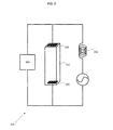
- FIG. 3 shows the pixel 102 configured in detection circuitry 300 .
- the detection circuitry 300 includes the pixel 102 (configured as a capacitor), and an inductor 302 , wherein the inductor and the capacitor formed by the pixel 102 form a resonant circuit.
- the detector may operate in either a poled (applied dc voltage bias) or non-poled configuration.
- the detection circuitry further includes circuitry 304 configured to determine at least one property of the resonant circuit, such as a resonant frequency.
- electromagnetic energy incident on the pixel 102 causes a change in dielectric constant of the pixel, thereby changing its capacitance, and thereby changing the resonant frequency of the resonant circuit, which is detected by the element 304 .
- the resonant frequency of the circuit changes according to the change in capacitance of the pixel, and thus the deviation from resonance would be a measure of the reduction in the dielectric constant, and be proportional to the intensity of the incident photons.
- FIG. 3 shows the pixel 102 configured as a capacitor, where parallel conductive plates 306 are placed at opposite ends of the pixel to form a capacitor.
- the placement and size of these conductive plates 306 are exemplary embodiments and may vary according to a particular embodiment.
- FIG. 3 shows the parallel conductive plates 306 being positioned on the short sides of the pixel, however in some embodiments the conductive plates 306 may be positioned along the longer sides of the pixel.
- the pixel may be configured as an inductor in a resonance circuit, operating on the same principals as a ferroelectric capacitor in a resonance circuit.
- FIG. 4 shows an array 400 of the pixels 102 of FIG. 1 together with detection circuitry 402 , where the detection circuitry may be configured as described with respect to FIG. 3 .
- the array of pixels is configured on a conductive ground plate 406 , and each pixel is configured with an individual conductive plate 408 such that the array of pixels forms an array of capacitors, where each of the capacitors is electrically connected to the detection circuitry.
- the pixels in the array are separated by a gap 404 , where the gap may be air or another insulator with dielectric or diamagnetic properties that do not change significantly compared to the detector material.
- the array of FIG. 4 is two dimensional, that is, the pixels are patterned along two dimensions, however this is just one exemplary embodiment, and in other embodiments, the array is one dimensional or three dimensional.
- the array 400 of pixels 102 forms an imaging system.
- the dimensions of the pixels 102 may be selected according to the considerations as previously described herein.
- the pixels are each operably connected to the detection circuitry 402 , and the detection circuitry may include a multichannel analyzer configured to identify which pixels have received photons.
- the pixel materials in the array are not all the same.
- pixels having different materials may be incorporated in an array where the materials have different ranges of electromagnetic energy they are capable of detecting, thus providing for a detector with a broader range of detection capability than a detector whose pixels are all the same.
- FIG. 5 shows another embodiment of an array 500 of pixels, where the array 500 shown in FIG. 5 is three dimensional.
- the detection circuitry is not shown in FIG. 5 , however in this embodiment each pixel 102 would be configured as a capacitor and would be operably connected to detection circuitry such that the presence of electromagnetic energy in each of the pixels could be detected.
- Such a three dimensional arrangement would allow the system to determine spatial information and information related to the energy of the incoming photons. For example, the energy of an incoming photon could determine how far the photon would travel in the detector, which could be determined according to which detectors receive electromagnetic energy.
- FIG. 6 shows an array of pixels 602 arranged in an imaging system, where in some embodiments such an imaging system is an x-ray imager.
- the system further comprises a source of x-rays 604 that is arranged to produce photons that can pass through a subject and be received by the array of pixels 602 .
- the system is a medical imaging system such as a pediatric imaging system, an emergency medical imaging system, or other type of medical imaging system.
- the system is a security system such as a system configured for airport security, for passengers or for objects.
- the system is a security system used for detection of gamma rays with energy in the range of MeV, sourced from special nuclear materials.
- the system is a medical system used to track the location of radioactive tags used in diagnostic medical imaging. There are many ways of configuring the imaging system and the system may be applied to a wide range of different subjects.
- the system includes detection circuitry (not shown) as previously described herein, where the detection circuitry is operably connected to the array of detection pixels and configured to measure a change in the first material produced by the Compton electrons, again as previously described herein.
- the detection circuitry is configured to compute a tomographic image of a subject, i.e., a CT scan.
- the source of x-rays and the array of detection pixels may be configured on a stage or other type of mount that is movable relative to a subject in order to scan the subject.
- the system may in some embodiments be configured to determine one or more properties corresponding to the incoming photons, such as an energy and/or an energy range, and/or an intensity.
- X-ray imaging for security and medicine have energies ranging from tens to hundreds of keV. In this energy range, there are two possible interaction mechanisms: Compton and photoelectric scattering.
- Compton scattering results in an ejected outer shell electron and a significant portion of the x-ray energy is transferred into the kinetic energy of the scattered electron.
- the photoelectric process involves scattering of inner-shell electrons, inducing an inner shell electronic transition where part of the energy is transferred to secondary x-ray photons.
- the Compton process results in a larger quantity of energy being dissipated in a smaller volume.
- the detector material should be of the appropriate atomic density so that the Compton process dominates the scattering at the operating energy of the x-ray source.
- the Compton process dominates at higher x-ray energies and lower (Z) detector density.
- Higher energy applications such as computed tomography and security screening, would use higher (averaged) atomic number detector materials such as PZT, whereas lower energy applications would use less dense materials such as LiNbO 3 .
- Calculation of the Compton cross-section also yields the average number of Compton electrons produced in the detector by a single photon, and thus the magnitude of the response (change in capacitance or inductance).
- k hv m e ⁇ c 2 .
- the effective scattering cross-section of the photoelectric effect in the non-relativistic treatment is:
- ⁇ photo 32 ⁇ 2 ⁇ ⁇ ⁇ ⁇ r 0 2 ⁇ ⁇ 4 3 ⁇ Z 5 ⁇ k - 7 / 2 , ( 3 )
- Compton ⁇ photo is plotted for the constituent atoms, as well as for PZT as a whole, as a function of incident photon energy.
- the data in FIG. 8 indicate that the relative contribution of Compton scattering in PZT is 5.6 at 100 keV, and 20.5 at 150 keV, yielding a Compton scattering probability of 84% and 95% respectively.
- the dielectric constant modification by local charging, as well as by the lattice distortions caused by electric charging may be obtained by quasi ab initio density functional theory (DFT) calculations.
- DFT quasi ab initio density functional theory
- the numerical calculation presented here is a concurrent cell and structure optimization performed at an externally applied isotropic pressure of 1.0 atm.
- the simulation is implemented with use of the Perdew-Burke-Ernzerhof (PBE) exchange correlation function with the appropriately selected basis functions.
- the simulation utilizes the Gaussian plane wave (GPW) approach to representing the electron wave-functions within the CP2K simulator.
- the basic structure of the calculation is the energy-optimized electrically neutral structure shown in FIG. 9 .
- Positive charge The electrically charged system (total charge +1e, or +e/8 per unit cell due to a leaving Compton electron, corresponding to the inner cone in FIG. 2 ), undergoes considerable local anisotropic strain, resulting in the following lattice periodicity values: X: 3.968 ⁇ (0.55% compression), Y: 3.932 ⁇ (1.45% compression), Z: 3.968 ⁇ (0.55% compression).
- Negative charge Extreme anisotropic strain is observed along the X-axis.
- the resulting lattice periodicity is: X: 5.06 ⁇ (27% stretching), Y: 3.86 ⁇ (3.26% compression), Z: 3.86 ⁇ (3.26% compression).
- the anisotropy of strain indicates a significant modification of the dielectric constant from direct theoretical calculations at high charge densities.
- the strain values can be used for an empirically based quantitative estimation of the dielectric constant modification. Existing experimental data or the measured PZT voltage/field-to-strain constants can be used for estimation.
- ⁇ f 1 ( 1 - E b ⁇ ⁇ i hc ) ⁇ ( ⁇ i + h mc ⁇ ( 1 - cos ⁇ ⁇ ⁇ ) ) , ( 4 )
- ⁇ i and ⁇ f are the photon wavelengths before and after a given scattering event, respectively; m, E b , and ⁇ are the electron's rest mass, the atomic binding energy, and the photon's scattering angle relative to its initial direction, respectively.
- the prefactor term does not play a significant role during the relatively early stages of the scattering process (E b ⁇ hc/ ⁇ i ), which is where Compton scattering dominates, as discussed above.
- the stochastic portion of the Monte Carlo simulation is set by the random scattering angle ⁇ of the recoiling Compton electron (relative to the photon's direction prior to each scattering event).
- the kinetic energy of the high-energy electrons is eventually converted to lattice vibrations.
- the highly transient effect of the initial lattice shockwaves generated by the electrons is of interest, as it contributes to disrupting the local polarizability of the material.
- N is the total number of perturbed regions (equal to the number of Compton electrons) and A and d are the cross-section and the height of the detector, respectively.
- a and d are the cross-section and the height of the detector, respectively.
- ⁇ ⁇ ⁇ C ⁇ 1 ⁇ ⁇ 0 ⁇ ⁇ ⁇ x ⁇ ( A - ⁇ ⁇ ⁇ ⁇ A ) + ⁇ 2 ⁇ ⁇ 0 ⁇ ⁇ ⁇ x ⁇ ( ⁇ ⁇ ⁇ ⁇ A ) , ( 7 )
- ⁇ ⁇ ⁇ C ⁇ 0 ⁇ ⁇ ⁇ x ⁇ ( A ⁇ ⁇ ⁇ 1 - N ⁇ ⁇ ⁇ ⁇ ⁇ A ⁇ ( ⁇ ⁇ ⁇ x d ) ⁇ ( ⁇ 1 - ⁇ 2 ) ) . ( 8 )
- ⁇ eff ⁇ 1 - ⁇ ⁇ t ⁇ ( ⁇ 1 - ⁇ 2 ) , ( 10 )
- ⁇ ⁇ t 10 - 3 , or 0.1%.
- the intrinsic dielectric constant of the material is high, the change is readily measurable through electronics based on resonance circuitry, or other forms.
Landscapes
- Chemical & Material Sciences (AREA)
- Health & Medical Sciences (AREA)
- General Physics & Mathematics (AREA)
- Immunology (AREA)
- Life Sciences & Earth Sciences (AREA)
- Analytical Chemistry (AREA)
- Biochemistry (AREA)
- General Health & Medical Sciences (AREA)
- Pathology (AREA)
- Physics & Mathematics (AREA)
- Crystallography & Structural Chemistry (AREA)
- Engineering & Computer Science (AREA)
- Nuclear Medicine, Radiotherapy & Molecular Imaging (AREA)
- Pulmonology (AREA)
- Radiology & Medical Imaging (AREA)
- Theoretical Computer Science (AREA)
- Measurement Of Radiation (AREA)
Abstract
Description
and wi are the mass attenuation constants of the constituent atoms and the corresponding atomic weight fractions, respectively. The resulting effective attenuation length calculated from the tabulated data is shown in
The value of k determines whether scattering occurs within the classical or the relativistic frame of reference associated with the moving electron. For the highest incoming photon energies considered below (150 keV), k=0.29, and thus relativistic effects do not play a significant role in these considerations. The effective scattering cross-section of the photoelectric effect in the non-relativistic treatment is:
is plotted for the constituent atoms, as well as for PZT as a whole, as a function of incident photon energy.
or 0.1%. As the intrinsic dielectric constant of the material is high, the change is readily measurable through electronics based on resonance circuitry, or other forms.
Claims (42)
Priority Applications (1)
| Application Number | Priority Date | Filing Date | Title |
|---|---|---|---|
| US15/379,006 US10126255B2 (en) | 2015-12-15 | 2016-12-14 | High efficiency photon detection |
Applications Claiming Priority (2)
| Application Number | Priority Date | Filing Date | Title |
|---|---|---|---|
| US201562267677P | 2015-12-15 | 2015-12-15 | |
| US15/379,006 US10126255B2 (en) | 2015-12-15 | 2016-12-14 | High efficiency photon detection |
Publications (2)
| Publication Number | Publication Date |
|---|---|
| US20170205361A1 US20170205361A1 (en) | 2017-07-20 |
| US10126255B2 true US10126255B2 (en) | 2018-11-13 |
Family
ID=59314560
Family Applications (1)
| Application Number | Title | Priority Date | Filing Date |
|---|---|---|---|
| US15/379,006 Active 2037-01-27 US10126255B2 (en) | 2015-12-15 | 2016-12-14 | High efficiency photon detection |
Country Status (3)
| Country | Link |
|---|---|
| US (1) | US10126255B2 (en) |
| CN (1) | CN108700673B (en) |
| WO (1) | WO2017155582A2 (en) |
Families Citing this family (4)
| Publication number | Priority date | Publication date | Assignee | Title |
|---|---|---|---|---|
| WO2020172861A1 (en) * | 2019-02-28 | 2020-09-03 | 深圳晶泰科技有限公司 | Quick collision detection method for crystal structure |
| CN110934604B (en) * | 2019-12-03 | 2023-06-27 | 上海联影医疗科技股份有限公司 | Compton scattering sequence recovery method, compton scattering sequence recovery device, storage medium and PET imaging system |
| CN112394072B (en) * | 2020-11-26 | 2021-10-22 | 西安石油大学 | Micro-CT-based core broadband dielectric constant characterization method and device |
| CN114355428B (en) * | 2022-01-05 | 2024-04-26 | 吉林大学 | Method for researching scintillator energy conversion mechanism |
Citations (4)
| Publication number | Priority date | Publication date | Assignee | Title |
|---|---|---|---|---|
| GB1471032A (en) * | 1973-03-26 | 1977-04-21 | Licentia Gmbh | Method of operating a pyro-electric detector |
| WO2008059425A2 (en) * | 2006-11-17 | 2008-05-22 | Koninklijke Philips Electronics N.V. | Radiation detector with multiple electrodes on a sensitive layer |
| US20090032717A1 (en) * | 2007-07-30 | 2009-02-05 | Siemens Medical Solutions Usa, Inc. | High-Resolution Depth-of-Interaction PET Detector |
| US20110122998A1 (en) * | 2008-08-07 | 2011-05-26 | Koninklijke Philips Electronics N.V. | Combined asg, cathode, and carrier for a photon detector |
Family Cites Families (9)
| Publication number | Priority date | Publication date | Assignee | Title |
|---|---|---|---|---|
| BE759910A (en) * | 1969-12-06 | 1971-06-04 | Philips Nv | MAGNETISABLE SUBSTANCE FOR DETECTION AND / OR RECORDING OF ELECTROMAGNETIC RADIATION AND ELECTRONS |
| US6448560B1 (en) * | 1996-02-02 | 2002-09-10 | Tumay O. Tumer | Method and apparatus for gamma ray detection |
| GB2401766B (en) * | 2003-03-11 | 2006-03-15 | Symetrica Ltd | Improved gamma-ray camera system |
| US8063379B2 (en) * | 2006-06-21 | 2011-11-22 | Avraham Suhami | Radiation cameras |
| US8111808B1 (en) * | 2008-08-15 | 2012-02-07 | Lockheed Martin Corporation | X-ray explosive imager |
| GB2466940B (en) * | 2008-12-12 | 2013-09-11 | Holdip Ltd | Improvements relating to resonant circuits |
| US8378310B2 (en) * | 2009-02-11 | 2013-02-19 | Prismatic Sensors Ab | Image quality in photon counting-mode detector systems |
| US10088580B2 (en) * | 2012-05-31 | 2018-10-02 | Minnesota Imaging And Engineering Llc | Detector systems for radiation imaging |
| US9057684B2 (en) * | 2013-04-05 | 2015-06-16 | The Arizona Board Of Regents On Behalf Of The University Of Arizona | Gamma ray imaging systems and methods |
-
2016
- 2016-12-14 CN CN201680081918.0A patent/CN108700673B/en not_active Expired - Fee Related
- 2016-12-14 WO PCT/US2016/066546 patent/WO2017155582A2/en active Application Filing
- 2016-12-14 US US15/379,006 patent/US10126255B2/en active Active
Patent Citations (4)
| Publication number | Priority date | Publication date | Assignee | Title |
|---|---|---|---|---|
| GB1471032A (en) * | 1973-03-26 | 1977-04-21 | Licentia Gmbh | Method of operating a pyro-electric detector |
| WO2008059425A2 (en) * | 2006-11-17 | 2008-05-22 | Koninklijke Philips Electronics N.V. | Radiation detector with multiple electrodes on a sensitive layer |
| US20090032717A1 (en) * | 2007-07-30 | 2009-02-05 | Siemens Medical Solutions Usa, Inc. | High-Resolution Depth-of-Interaction PET Detector |
| US20110122998A1 (en) * | 2008-08-07 | 2011-05-26 | Koninklijke Philips Electronics N.V. | Combined asg, cathode, and carrier for a photon detector |
Non-Patent Citations (4)
| Title |
|---|
| A.A. de Carvalho, A.L. Brassalotti, M.H. de Paula and A.J. Alter, Use of lithium niobate detector for measuring X-ray intensity in mammographic range, Electronics Letters Sep. 2, 2004, vol. 40, No. 18, 2 pages. |
| D.B. Li, D.R. Strachan, J.H. Ferris and D.A. Bonnell, Polarization reorientation in ferroelectric lead zirconate titanate thin films with electrons beams, J. Mater. Res., vol. 21, No. 4, April, pp. 935-940. |
| M J Yaffe and J A Rowlands, Imaging Research Program, Sunnybrook Health Science Centre, The University of Toronto, Phys. Med. Biol. 42 (1997)1-39. Printed in the UK, n final form Aug. 16, 1996, 30 pages. |
| W. Lee et al., Letters, Individually addressable epitaxial ferroelectric nanocapacitor arrays with near Tb inch-2 density, Published online: Jun. 15, 2008; doi: 10.1038/nnano/2008.161, nature nanotechnology, vol. 3, Jul. 2008, 6 pages. |
Also Published As
| Publication number | Publication date |
|---|---|
| US20170205361A1 (en) | 2017-07-20 |
| WO2017155582A2 (en) | 2017-09-14 |
| WO2017155582A3 (en) | 2017-11-23 |
| CN108700673A (en) | 2018-10-23 |
| CN108700673B (en) | 2022-05-31 |
Similar Documents
| Publication | Publication Date | Title |
|---|---|---|
| US10126255B2 (en) | High efficiency photon detection | |
| Baldwin et al. | X-ray yield curves for γ− n reactions | |
| US10031244B2 (en) | Detectors, system and method for detecting ionizing radiation using high energy current | |
| Behm et al. | A spectrometer for ultrashort gamma-ray pulses with photon energies greater than 10 MeV | |
| Bilki et al. | Measurement of the rate capability of Resistive Plate Chambers | |
| Suliman et al. | Gamma beam industrial applications at ELI-NP | |
| Salgado et al. | Single particle detection system for strong-field QED experiments | |
| Prencipe et al. | Efficient laser-driven proton and bremsstrahlung generation from cluster-assembled foam targets | |
| Deppner et al. | The CBM Time-of-Flight wall—a conceptual design | |
| Tsuzuki et al. | An application of a Si/CdTe Compton camera for the polarization measurement of hard x rays from highly charged heavy ions | |
| Manuel et al. | Enhanced spatial resolution of Eljen-204 plastic scintillators for use in rep-rated proton diagnostics | |
| Cester et al. | A compact neutron–gamma spectrometer | |
| Tao et al. | Simulation studies to understand sensitivity and timing characteristics of an optical property modulation-based radiation detection concept for PET | |
| Brivio et al. | Nanoporous aerogel-based periodic high-energy electron current x-ray sensors | |
| Harkness et al. | Characterisation of a Si (Li) orthogonal-strip detector | |
| Zahradnik et al. | A diamond guard ring microdosimeter for ion beam therapy | |
| Muraro et al. | Performance of the full size nGEM detector for the SPIDER experiment | |
| Rathore et al. | Calculation of spatial response of a collimated segmented HPGe detector for gamma emission tomography by MCNP simulations | |
| Persson et al. | Simulation model for evaluating energy-resolving photon-counting CT detectors based on generalized linear-systems framework | |
| Morris et al. | A new method for imaging nuclear threats using cosmic ray muons | |
| Quiter et al. | Developing a diagnostic for energetic laser-Compton produced photon beams | |
| Spicer et al. | The Giant Resonance of Photodisintegration of Tantalum | |
| Miyachi et al. | Acoustic signals generated in piezoelectric lead–zirconate–titanate elements by direct bombardment with xenon ions | |
| Miyachi et al. | Response of acoustic signals generated in water by energetic xenon ions | |
| Weber et al. | Compton polarimeters for the study of hard X-rays arising from energetic collisions of electrons and ions with matter |
Legal Events
| Date | Code | Title | Description |
|---|---|---|---|
| AS | Assignment |
Owner name: ELWHA LLC, WASHINGTON Free format text: ASSIGNMENT OF ASSIGNORS INTEREST;ASSIGNORS:CANNARA, RACHEL;SARIFI, FRED;SMOLYANITSKY, ALEX;SIGNING DATES FROM 20170221 TO 20170310;REEL/FRAME:041562/0188 |
|
| STCF | Information on status: patent grant |
Free format text: PATENTED CASE |
|
| AS | Assignment |
Owner name: GOVERNMENT OF THE UNITED STATES OF AMERICA, AS REP Free format text: ASSIGNMENT OF ASSIGNORS INTEREST;ASSIGNOR:SMOLYANITSKY, ALEX;REEL/FRAME:048784/0832 Effective date: 20190320 |
|
| MAFP | Maintenance fee payment |
Free format text: PAYMENT OF MAINTENANCE FEE, 4TH YEAR, LARGE ENTITY (ORIGINAL EVENT CODE: M1551); ENTITY STATUS OF PATENT OWNER: LARGE ENTITY Year of fee payment: 4 |
|
| AS | Assignment |
Owner name: THE INVENTION SCIENCE FUND II, LLC, WASHINGTON Free format text: ASSIGNMENT OF ASSIGNORS INTEREST;ASSIGNOR:ELWHA LLC;REEL/FRAME:066732/0618 Effective date: 20240220 Owner name: CARILLON TECHNOLOGIES LLC, VIRGINIA Free format text: ASSIGNMENT OF ASSIGNORS INTEREST;ASSIGNOR:THE INVENTION SCIENCE FUND II, LLC;REEL/FRAME:066733/0579 Effective date: 20240220 |