US10125014B2 - Integrated circuit package and method of forming same - Google Patents
Integrated circuit package and method of forming same Download PDFInfo
- Publication number
- US10125014B2 US10125014B2 US15/843,372 US201715843372A US10125014B2 US 10125014 B2 US10125014 B2 US 10125014B2 US 201715843372 A US201715843372 A US 201715843372A US 10125014 B2 US10125014 B2 US 10125014B2
- Authority
- US
- United States
- Prior art keywords
- die
- dies
- contact
- encapsulant
- rdls
- Prior art date
- Legal status (The legal status is an assumption and is not a legal conclusion. Google has not performed a legal analysis and makes no representation as to the accuracy of the status listed.)
- Active
Links
Images


Classifications
-
- B—PERFORMING OPERATIONS; TRANSPORTING
- B81—MICROSTRUCTURAL TECHNOLOGY
- B81C—PROCESSES OR APPARATUS SPECIALLY ADAPTED FOR THE MANUFACTURE OR TREATMENT OF MICROSTRUCTURAL DEVICES OR SYSTEMS
- B81C1/00—Manufacture or treatment of devices or systems in or on a substrate
- B81C1/00015—Manufacture or treatment of devices or systems in or on a substrate for manufacturing microsystems
- B81C1/00222—Integrating an electronic processing unit with a micromechanical structure
- B81C1/0023—Packaging together an electronic processing unit die and a micromechanical structure die
-
- H—ELECTRICITY
- H01—ELECTRIC ELEMENTS
- H01L—SEMICONDUCTOR DEVICES NOT COVERED BY CLASS H10
- H01L24/00—Arrangements for connecting or disconnecting semiconductor or solid-state bodies; Methods or apparatus related thereto
- H01L24/01—Means for bonding being attached to, or being formed on, the surface to be connected, e.g. chip-to-package, die-attach, "first-level" interconnects; Manufacturing methods related thereto
- H01L24/02—Bonding areas ; Manufacturing methods related thereto
- H01L24/03—Manufacturing methods
-
- B—PERFORMING OPERATIONS; TRANSPORTING
- B81—MICROSTRUCTURAL TECHNOLOGY
- B81B—MICROSTRUCTURAL DEVICES OR SYSTEMS, e.g. MICROMECHANICAL DEVICES
- B81B7/00—Microstructural systems; Auxiliary parts of microstructural devices or systems
- B81B7/0032—Packages or encapsulation
- B81B7/007—Interconnections between the MEMS and external electrical signals
-
- B—PERFORMING OPERATIONS; TRANSPORTING
- B81—MICROSTRUCTURAL TECHNOLOGY
- B81C—PROCESSES OR APPARATUS SPECIALLY ADAPTED FOR THE MANUFACTURE OR TREATMENT OF MICROSTRUCTURAL DEVICES OR SYSTEMS
- B81C1/00—Manufacture or treatment of devices or systems in or on a substrate
- B81C1/00865—Multistep processes for the separation of wafers into individual elements
- B81C1/00888—Multistep processes involving only mechanical separation, e.g. grooving followed by cleaving
-
- H—ELECTRICITY
- H01—ELECTRIC ELEMENTS
- H01L—SEMICONDUCTOR DEVICES NOT COVERED BY CLASS H10
- H01L21/00—Processes or apparatus adapted for the manufacture or treatment of semiconductor or solid state devices or of parts thereof
- H01L21/02—Manufacture or treatment of semiconductor devices or of parts thereof
- H01L21/04—Manufacture or treatment of semiconductor devices or of parts thereof the devices having at least one potential-jump barrier or surface barrier, e.g. PN junction, depletion layer or carrier concentration layer
- H01L21/50—Assembly of semiconductor devices using processes or apparatus not provided for in a single one of the subgroups H01L21/06 - H01L21/326, e.g. sealing of a cap to a base of a container
- H01L21/56—Encapsulations, e.g. encapsulation layers, coatings
- H01L21/561—Batch processing
-
- H—ELECTRICITY
- H01—ELECTRIC ELEMENTS
- H01L—SEMICONDUCTOR DEVICES NOT COVERED BY CLASS H10
- H01L21/00—Processes or apparatus adapted for the manufacture or treatment of semiconductor or solid state devices or of parts thereof
- H01L21/02—Manufacture or treatment of semiconductor devices or of parts thereof
- H01L21/04—Manufacture or treatment of semiconductor devices or of parts thereof the devices having at least one potential-jump barrier or surface barrier, e.g. PN junction, depletion layer or carrier concentration layer
- H01L21/50—Assembly of semiconductor devices using processes or apparatus not provided for in a single one of the subgroups H01L21/06 - H01L21/326, e.g. sealing of a cap to a base of a container
- H01L21/56—Encapsulations, e.g. encapsulation layers, coatings
- H01L21/565—Moulds
-
- H—ELECTRICITY
- H01—ELECTRIC ELEMENTS
- H01L—SEMICONDUCTOR DEVICES NOT COVERED BY CLASS H10
- H01L23/00—Details of semiconductor or other solid state devices
- H01L23/12—Mountings, e.g. non-detachable insulating substrates
- H01L23/13—Mountings, e.g. non-detachable insulating substrates characterised by the shape
-
- H—ELECTRICITY
- H01—ELECTRIC ELEMENTS
- H01L—SEMICONDUCTOR DEVICES NOT COVERED BY CLASS H10
- H01L23/00—Details of semiconductor or other solid state devices
- H01L23/28—Encapsulations, e.g. encapsulating layers, coatings, e.g. for protection
- H01L23/31—Encapsulations, e.g. encapsulating layers, coatings, e.g. for protection characterised by the arrangement or shape
- H01L23/3107—Encapsulations, e.g. encapsulating layers, coatings, e.g. for protection characterised by the arrangement or shape the device being completely enclosed
- H01L23/3121—Encapsulations, e.g. encapsulating layers, coatings, e.g. for protection characterised by the arrangement or shape the device being completely enclosed a substrate forming part of the encapsulation
-
- H—ELECTRICITY
- H01—ELECTRIC ELEMENTS
- H01L—SEMICONDUCTOR DEVICES NOT COVERED BY CLASS H10
- H01L23/00—Details of semiconductor or other solid state devices
- H01L23/48—Arrangements for conducting electric current to or from the solid state body in operation, e.g. leads, terminal arrangements ; Selection of materials therefor
- H01L23/481—Internal lead connections, e.g. via connections, feedthrough structures
-
- H—ELECTRICITY
- H01—ELECTRIC ELEMENTS
- H01L—SEMICONDUCTOR DEVICES NOT COVERED BY CLASS H10
- H01L23/00—Details of semiconductor or other solid state devices
- H01L23/48—Arrangements for conducting electric current to or from the solid state body in operation, e.g. leads, terminal arrangements ; Selection of materials therefor
- H01L23/488—Arrangements for conducting electric current to or from the solid state body in operation, e.g. leads, terminal arrangements ; Selection of materials therefor consisting of soldered or bonded constructions
- H01L23/498—Leads, i.e. metallisations or lead-frames on insulating substrates, e.g. chip carriers
- H01L23/49838—Geometry or layout
-
- H—ELECTRICITY
- H01—ELECTRIC ELEMENTS
- H01L—SEMICONDUCTOR DEVICES NOT COVERED BY CLASS H10
- H01L23/00—Details of semiconductor or other solid state devices
- H01L23/52—Arrangements for conducting electric current within the device in operation from one component to another, i.e. interconnections, e.g. wires, lead frames
- H01L23/538—Arrangements for conducting electric current within the device in operation from one component to another, i.e. interconnections, e.g. wires, lead frames the interconnection structure between a plurality of semiconductor chips being formed on, or in, insulating substrates
- H01L23/5383—Multilayer substrates
-
- H—ELECTRICITY
- H01—ELECTRIC ELEMENTS
- H01L—SEMICONDUCTOR DEVICES NOT COVERED BY CLASS H10
- H01L23/00—Details of semiconductor or other solid state devices
- H01L23/52—Arrangements for conducting electric current within the device in operation from one component to another, i.e. interconnections, e.g. wires, lead frames
- H01L23/538—Arrangements for conducting electric current within the device in operation from one component to another, i.e. interconnections, e.g. wires, lead frames the interconnection structure between a plurality of semiconductor chips being formed on, or in, insulating substrates
- H01L23/5384—Conductive vias through the substrate with or without pins, e.g. buried coaxial conductors
-
- H—ELECTRICITY
- H01—ELECTRIC ELEMENTS
- H01L—SEMICONDUCTOR DEVICES NOT COVERED BY CLASS H10
- H01L23/00—Details of semiconductor or other solid state devices
- H01L23/52—Arrangements for conducting electric current within the device in operation from one component to another, i.e. interconnections, e.g. wires, lead frames
- H01L23/538—Arrangements for conducting electric current within the device in operation from one component to another, i.e. interconnections, e.g. wires, lead frames the interconnection structure between a plurality of semiconductor chips being formed on, or in, insulating substrates
- H01L23/5385—Assembly of a plurality of insulating substrates
-
- H—ELECTRICITY
- H01—ELECTRIC ELEMENTS
- H01L—SEMICONDUCTOR DEVICES NOT COVERED BY CLASS H10
- H01L24/00—Arrangements for connecting or disconnecting semiconductor or solid-state bodies; Methods or apparatus related thereto
- H01L24/01—Means for bonding being attached to, or being formed on, the surface to be connected, e.g. chip-to-package, die-attach, "first-level" interconnects; Manufacturing methods related thereto
- H01L24/02—Bonding areas ; Manufacturing methods related thereto
- H01L24/07—Structure, shape, material or disposition of the bonding areas after the connecting process
- H01L24/09—Structure, shape, material or disposition of the bonding areas after the connecting process of a plurality of bonding areas
-
- H—ELECTRICITY
- H01—ELECTRIC ELEMENTS
- H01L—SEMICONDUCTOR DEVICES NOT COVERED BY CLASS H10
- H01L24/00—Arrangements for connecting or disconnecting semiconductor or solid-state bodies; Methods or apparatus related thereto
- H01L24/01—Means for bonding being attached to, or being formed on, the surface to be connected, e.g. chip-to-package, die-attach, "first-level" interconnects; Manufacturing methods related thereto
- H01L24/18—High density interconnect [HDI] connectors; Manufacturing methods related thereto
- H01L24/19—Manufacturing methods of high density interconnect preforms
-
- H—ELECTRICITY
- H01—ELECTRIC ELEMENTS
- H01L—SEMICONDUCTOR DEVICES NOT COVERED BY CLASS H10
- H01L24/00—Arrangements for connecting or disconnecting semiconductor or solid-state bodies; Methods or apparatus related thereto
- H01L24/01—Means for bonding being attached to, or being formed on, the surface to be connected, e.g. chip-to-package, die-attach, "first-level" interconnects; Manufacturing methods related thereto
- H01L24/18—High density interconnect [HDI] connectors; Manufacturing methods related thereto
- H01L24/20—Structure, shape, material or disposition of high density interconnect preforms
-
- H—ELECTRICITY
- H01—ELECTRIC ELEMENTS
- H01L—SEMICONDUCTOR DEVICES NOT COVERED BY CLASS H10
- H01L24/00—Arrangements for connecting or disconnecting semiconductor or solid-state bodies; Methods or apparatus related thereto
- H01L24/01—Means for bonding being attached to, or being formed on, the surface to be connected, e.g. chip-to-package, die-attach, "first-level" interconnects; Manufacturing methods related thereto
- H01L24/26—Layer connectors, e.g. plate connectors, solder or adhesive layers; Manufacturing methods related thereto
- H01L24/27—Manufacturing methods
-
- H—ELECTRICITY
- H01—ELECTRIC ELEMENTS
- H01L—SEMICONDUCTOR DEVICES NOT COVERED BY CLASS H10
- H01L24/00—Arrangements for connecting or disconnecting semiconductor or solid-state bodies; Methods or apparatus related thereto
- H01L24/93—Batch processes
- H01L24/95—Batch processes at chip-level, i.e. with connecting carried out on a plurality of singulated devices, i.e. on diced chips
- H01L24/96—Batch processes at chip-level, i.e. with connecting carried out on a plurality of singulated devices, i.e. on diced chips the devices being encapsulated in a common layer, e.g. neo-wafer or pseudo-wafer, said common layer being separable into individual assemblies after connecting
-
- H—ELECTRICITY
- H01—ELECTRIC ELEMENTS
- H01L—SEMICONDUCTOR DEVICES NOT COVERED BY CLASS H10
- H01L25/00—Assemblies consisting of a plurality of individual semiconductor or other solid state devices ; Multistep manufacturing processes thereof
- H01L25/16—Assemblies consisting of a plurality of individual semiconductor or other solid state devices ; Multistep manufacturing processes thereof the devices being of types provided for in two or more different main groups of groups H01L27/00 - H01L33/00, or in a single subclass of H10K, H10N, e.g. forming hybrid circuits
-
- H—ELECTRICITY
- H01—ELECTRIC ELEMENTS
- H01L—SEMICONDUCTOR DEVICES NOT COVERED BY CLASS H10
- H01L25/00—Assemblies consisting of a plurality of individual semiconductor or other solid state devices ; Multistep manufacturing processes thereof
- H01L25/18—Assemblies consisting of a plurality of individual semiconductor or other solid state devices ; Multistep manufacturing processes thereof the devices being of types provided for in two or more different subgroups of the same main group of groups H01L27/00 - H01L33/00, or in a single subclass of H10K, H10N
-
- H—ELECTRICITY
- H05—ELECTRIC TECHNIQUES NOT OTHERWISE PROVIDED FOR
- H05K—PRINTED CIRCUITS; CASINGS OR CONSTRUCTIONAL DETAILS OF ELECTRIC APPARATUS; MANUFACTURE OF ASSEMBLAGES OF ELECTRICAL COMPONENTS
- H05K999/00—PRINTED CIRCUITS; CASINGS OR CONSTRUCTIONAL DETAILS OF ELECTRIC APPARATUS; MANUFACTURE OF ASSEMBLAGES OF ELECTRICAL COMPONENTS dummy group
- H05K999/99—PRINTED CIRCUITS; CASINGS OR CONSTRUCTIONAL DETAILS OF ELECTRIC APPARATUS; MANUFACTURE OF ASSEMBLAGES OF ELECTRICAL COMPONENTS dummy group dummy group
-
- B—PERFORMING OPERATIONS; TRANSPORTING
- B81—MICROSTRUCTURAL TECHNOLOGY
- B81B—MICROSTRUCTURAL DEVICES OR SYSTEMS, e.g. MICROMECHANICAL DEVICES
- B81B2207/00—Microstructural systems or auxiliary parts thereof
- B81B2207/01—Microstructural systems or auxiliary parts thereof comprising a micromechanical device connected to control or processing electronics, i.e. Smart-MEMS
- B81B2207/012—Microstructural systems or auxiliary parts thereof comprising a micromechanical device connected to control or processing electronics, i.e. Smart-MEMS the micromechanical device and the control or processing electronics being separate parts in the same package
-
- B—PERFORMING OPERATIONS; TRANSPORTING
- B81—MICROSTRUCTURAL TECHNOLOGY
- B81B—MICROSTRUCTURAL DEVICES OR SYSTEMS, e.g. MICROMECHANICAL DEVICES
- B81B2207/00—Microstructural systems or auxiliary parts thereof
- B81B2207/07—Interconnects
-
- B—PERFORMING OPERATIONS; TRANSPORTING
- B81—MICROSTRUCTURAL TECHNOLOGY
- B81C—PROCESSES OR APPARATUS SPECIALLY ADAPTED FOR THE MANUFACTURE OR TREATMENT OF MICROSTRUCTURAL DEVICES OR SYSTEMS
- B81C2203/00—Forming microstructural systems
- B81C2203/07—Integrating an electronic processing unit with a micromechanical structure
- B81C2203/0785—Transfer and j oin technology, i.e. forming the electronic processing unit and the micromechanical structure on separate substrates and joining the substrates
- B81C2203/0792—Forming interconnections between the electronic processing unit and the micromechanical structure
-
- H—ELECTRICITY
- H01—ELECTRIC ELEMENTS
- H01L—SEMICONDUCTOR DEVICES NOT COVERED BY CLASS H10
- H01L21/00—Processes or apparatus adapted for the manufacture or treatment of semiconductor or solid state devices or of parts thereof
- H01L21/02—Manufacture or treatment of semiconductor devices or of parts thereof
- H01L21/04—Manufacture or treatment of semiconductor devices or of parts thereof the devices having at least one potential-jump barrier or surface barrier, e.g. PN junction, depletion layer or carrier concentration layer
- H01L21/50—Assembly of semiconductor devices using processes or apparatus not provided for in a single one of the subgroups H01L21/06 - H01L21/326, e.g. sealing of a cap to a base of a container
- H01L21/56—Encapsulations, e.g. encapsulation layers, coatings
- H01L21/568—Temporary substrate used as encapsulation process aid
-
- H—ELECTRICITY
- H01—ELECTRIC ELEMENTS
- H01L—SEMICONDUCTOR DEVICES NOT COVERED BY CLASS H10
- H01L2224/00—Indexing scheme for arrangements for connecting or disconnecting semiconductor or solid-state bodies and methods related thereto as covered by H01L24/00
- H01L2224/01—Means for bonding being attached to, or being formed on, the surface to be connected, e.g. chip-to-package, die-attach, "first-level" interconnects; Manufacturing methods related thereto
- H01L2224/02—Bonding areas; Manufacturing methods related thereto
- H01L2224/023—Redistribution layers [RDL] for bonding areas
- H01L2224/0231—Manufacturing methods of the redistribution layers
-
- H—ELECTRICITY
- H01—ELECTRIC ELEMENTS
- H01L—SEMICONDUCTOR DEVICES NOT COVERED BY CLASS H10
- H01L2224/00—Indexing scheme for arrangements for connecting or disconnecting semiconductor or solid-state bodies and methods related thereto as covered by H01L24/00
- H01L2224/01—Means for bonding being attached to, or being formed on, the surface to be connected, e.g. chip-to-package, die-attach, "first-level" interconnects; Manufacturing methods related thereto
- H01L2224/02—Bonding areas; Manufacturing methods related thereto
- H01L2224/04—Structure, shape, material or disposition of the bonding areas prior to the connecting process
- H01L2224/0401—Bonding areas specifically adapted for bump connectors, e.g. under bump metallisation [UBM]
-
- H—ELECTRICITY
- H01—ELECTRIC ELEMENTS
- H01L—SEMICONDUCTOR DEVICES NOT COVERED BY CLASS H10
- H01L2224/00—Indexing scheme for arrangements for connecting or disconnecting semiconductor or solid-state bodies and methods related thereto as covered by H01L24/00
- H01L2224/01—Means for bonding being attached to, or being formed on, the surface to be connected, e.g. chip-to-package, die-attach, "first-level" interconnects; Manufacturing methods related thereto
- H01L2224/02—Bonding areas; Manufacturing methods related thereto
- H01L2224/04—Structure, shape, material or disposition of the bonding areas prior to the connecting process
- H01L2224/04105—Bonding areas formed on an encapsulation of the semiconductor or solid-state body, e.g. bonding areas on chip-scale packages
-
- H—ELECTRICITY
- H01—ELECTRIC ELEMENTS
- H01L—SEMICONDUCTOR DEVICES NOT COVERED BY CLASS H10
- H01L2224/00—Indexing scheme for arrangements for connecting or disconnecting semiconductor or solid-state bodies and methods related thereto as covered by H01L24/00
- H01L2224/01—Means for bonding being attached to, or being formed on, the surface to be connected, e.g. chip-to-package, die-attach, "first-level" interconnects; Manufacturing methods related thereto
- H01L2224/02—Bonding areas; Manufacturing methods related thereto
- H01L2224/04—Structure, shape, material or disposition of the bonding areas prior to the connecting process
- H01L2224/05—Structure, shape, material or disposition of the bonding areas prior to the connecting process of an individual bonding area
- H01L2224/05001—Internal layers
- H01L2224/0502—Disposition
- H01L2224/05024—Disposition the internal layer being disposed on a redistribution layer on the semiconductor or solid-state body
-
- H—ELECTRICITY
- H01—ELECTRIC ELEMENTS
- H01L—SEMICONDUCTOR DEVICES NOT COVERED BY CLASS H10
- H01L2224/00—Indexing scheme for arrangements for connecting or disconnecting semiconductor or solid-state bodies and methods related thereto as covered by H01L24/00
- H01L2224/01—Means for bonding being attached to, or being formed on, the surface to be connected, e.g. chip-to-package, die-attach, "first-level" interconnects; Manufacturing methods related thereto
- H01L2224/02—Bonding areas; Manufacturing methods related thereto
- H01L2224/04—Structure, shape, material or disposition of the bonding areas prior to the connecting process
- H01L2224/05—Structure, shape, material or disposition of the bonding areas prior to the connecting process of an individual bonding area
- H01L2224/05001—Internal layers
- H01L2224/0502—Disposition
- H01L2224/05025—Disposition the internal layer being disposed on a via connection of the semiconductor or solid-state body
-
- H—ELECTRICITY
- H01—ELECTRIC ELEMENTS
- H01L—SEMICONDUCTOR DEVICES NOT COVERED BY CLASS H10
- H01L2224/00—Indexing scheme for arrangements for connecting or disconnecting semiconductor or solid-state bodies and methods related thereto as covered by H01L24/00
- H01L2224/01—Means for bonding being attached to, or being formed on, the surface to be connected, e.g. chip-to-package, die-attach, "first-level" interconnects; Manufacturing methods related thereto
- H01L2224/02—Bonding areas; Manufacturing methods related thereto
- H01L2224/07—Structure, shape, material or disposition of the bonding areas after the connecting process
- H01L2224/08—Structure, shape, material or disposition of the bonding areas after the connecting process of an individual bonding area
- H01L2224/081—Disposition
- H01L2224/0812—Disposition the bonding area connecting directly to another bonding area, i.e. connectorless bonding, e.g. bumpless bonding
- H01L2224/08151—Disposition the bonding area connecting directly to another bonding area, i.e. connectorless bonding, e.g. bumpless bonding the bonding area connecting between a semiconductor or solid-state body and an item not being a semiconductor or solid-state body, e.g. chip-to-substrate, chip-to-passive
- H01L2224/08221—Disposition the bonding area connecting directly to another bonding area, i.e. connectorless bonding, e.g. bumpless bonding the bonding area connecting between a semiconductor or solid-state body and an item not being a semiconductor or solid-state body, e.g. chip-to-substrate, chip-to-passive the body and the item being stacked
- H01L2224/08225—Disposition the bonding area connecting directly to another bonding area, i.e. connectorless bonding, e.g. bumpless bonding the bonding area connecting between a semiconductor or solid-state body and an item not being a semiconductor or solid-state body, e.g. chip-to-substrate, chip-to-passive the body and the item being stacked the item being non-metallic, e.g. insulating substrate with or without metallisation
-
- H—ELECTRICITY
- H01—ELECTRIC ELEMENTS
- H01L—SEMICONDUCTOR DEVICES NOT COVERED BY CLASS H10
- H01L2224/00—Indexing scheme for arrangements for connecting or disconnecting semiconductor or solid-state bodies and methods related thereto as covered by H01L24/00
- H01L2224/01—Means for bonding being attached to, or being formed on, the surface to be connected, e.g. chip-to-package, die-attach, "first-level" interconnects; Manufacturing methods related thereto
- H01L2224/10—Bump connectors; Manufacturing methods related thereto
- H01L2224/11—Manufacturing methods
- H01L2224/113—Manufacturing methods by local deposition of the material of the bump connector
- H01L2224/1131—Manufacturing methods by local deposition of the material of the bump connector in liquid form
- H01L2224/1132—Screen printing, i.e. using a stencil
-
- H—ELECTRICITY
- H01—ELECTRIC ELEMENTS
- H01L—SEMICONDUCTOR DEVICES NOT COVERED BY CLASS H10
- H01L2224/00—Indexing scheme for arrangements for connecting or disconnecting semiconductor or solid-state bodies and methods related thereto as covered by H01L24/00
- H01L2224/01—Means for bonding being attached to, or being formed on, the surface to be connected, e.g. chip-to-package, die-attach, "first-level" interconnects; Manufacturing methods related thereto
- H01L2224/10—Bump connectors; Manufacturing methods related thereto
- H01L2224/11—Manufacturing methods
- H01L2224/113—Manufacturing methods by local deposition of the material of the bump connector
- H01L2224/1133—Manufacturing methods by local deposition of the material of the bump connector in solid form
- H01L2224/11334—Manufacturing methods by local deposition of the material of the bump connector in solid form using preformed bumps
-
- H—ELECTRICITY
- H01—ELECTRIC ELEMENTS
- H01L—SEMICONDUCTOR DEVICES NOT COVERED BY CLASS H10
- H01L2224/00—Indexing scheme for arrangements for connecting or disconnecting semiconductor or solid-state bodies and methods related thereto as covered by H01L24/00
- H01L2224/01—Means for bonding being attached to, or being formed on, the surface to be connected, e.g. chip-to-package, die-attach, "first-level" interconnects; Manufacturing methods related thereto
- H01L2224/10—Bump connectors; Manufacturing methods related thereto
- H01L2224/11—Manufacturing methods
- H01L2224/114—Manufacturing methods by blanket deposition of the material of the bump connector
- H01L2224/1141—Manufacturing methods by blanket deposition of the material of the bump connector in liquid form
- H01L2224/11424—Immersion coating, e.g. in a solder bath
-
- H—ELECTRICITY
- H01—ELECTRIC ELEMENTS
- H01L—SEMICONDUCTOR DEVICES NOT COVERED BY CLASS H10
- H01L2224/00—Indexing scheme for arrangements for connecting or disconnecting semiconductor or solid-state bodies and methods related thereto as covered by H01L24/00
- H01L2224/01—Means for bonding being attached to, or being formed on, the surface to be connected, e.g. chip-to-package, die-attach, "first-level" interconnects; Manufacturing methods related thereto
- H01L2224/10—Bump connectors; Manufacturing methods related thereto
- H01L2224/11—Manufacturing methods
- H01L2224/114—Manufacturing methods by blanket deposition of the material of the bump connector
- H01L2224/11444—Manufacturing methods by blanket deposition of the material of the bump connector in gaseous form
- H01L2224/1145—Physical vapour deposition [PVD], e.g. evaporation, or sputtering
-
- H—ELECTRICITY
- H01—ELECTRIC ELEMENTS
- H01L—SEMICONDUCTOR DEVICES NOT COVERED BY CLASS H10
- H01L2224/00—Indexing scheme for arrangements for connecting or disconnecting semiconductor or solid-state bodies and methods related thereto as covered by H01L24/00
- H01L2224/01—Means for bonding being attached to, or being formed on, the surface to be connected, e.g. chip-to-package, die-attach, "first-level" interconnects; Manufacturing methods related thereto
- H01L2224/10—Bump connectors; Manufacturing methods related thereto
- H01L2224/11—Manufacturing methods
- H01L2224/114—Manufacturing methods by blanket deposition of the material of the bump connector
- H01L2224/1146—Plating
- H01L2224/11462—Electroplating
-
- H—ELECTRICITY
- H01—ELECTRIC ELEMENTS
- H01L—SEMICONDUCTOR DEVICES NOT COVERED BY CLASS H10
- H01L2224/00—Indexing scheme for arrangements for connecting or disconnecting semiconductor or solid-state bodies and methods related thereto as covered by H01L24/00
- H01L2224/01—Means for bonding being attached to, or being formed on, the surface to be connected, e.g. chip-to-package, die-attach, "first-level" interconnects; Manufacturing methods related thereto
- H01L2224/10—Bump connectors; Manufacturing methods related thereto
- H01L2224/11—Manufacturing methods
- H01L2224/114—Manufacturing methods by blanket deposition of the material of the bump connector
- H01L2224/1146—Plating
- H01L2224/11464—Electroless plating
-
- H—ELECTRICITY
- H01—ELECTRIC ELEMENTS
- H01L—SEMICONDUCTOR DEVICES NOT COVERED BY CLASS H10
- H01L2224/00—Indexing scheme for arrangements for connecting or disconnecting semiconductor or solid-state bodies and methods related thereto as covered by H01L24/00
- H01L2224/01—Means for bonding being attached to, or being formed on, the surface to be connected, e.g. chip-to-package, die-attach, "first-level" interconnects; Manufacturing methods related thereto
- H01L2224/10—Bump connectors; Manufacturing methods related thereto
- H01L2224/11—Manufacturing methods
- H01L2224/118—Post-treatment of the bump connector
- H01L2224/11848—Thermal treatments, e.g. annealing, controlled cooling
- H01L2224/11849—Reflowing
-
- H—ELECTRICITY
- H01—ELECTRIC ELEMENTS
- H01L—SEMICONDUCTOR DEVICES NOT COVERED BY CLASS H10
- H01L2224/00—Indexing scheme for arrangements for connecting or disconnecting semiconductor or solid-state bodies and methods related thereto as covered by H01L24/00
- H01L2224/01—Means for bonding being attached to, or being formed on, the surface to be connected, e.g. chip-to-package, die-attach, "first-level" interconnects; Manufacturing methods related thereto
- H01L2224/10—Bump connectors; Manufacturing methods related thereto
- H01L2224/12—Structure, shape, material or disposition of the bump connectors prior to the connecting process
- H01L2224/12105—Bump connectors formed on an encapsulation of the semiconductor or solid-state body, e.g. bumps on chip-scale packages
-
- H—ELECTRICITY
- H01—ELECTRIC ELEMENTS
- H01L—SEMICONDUCTOR DEVICES NOT COVERED BY CLASS H10
- H01L2224/00—Indexing scheme for arrangements for connecting or disconnecting semiconductor or solid-state bodies and methods related thereto as covered by H01L24/00
- H01L2224/01—Means for bonding being attached to, or being formed on, the surface to be connected, e.g. chip-to-package, die-attach, "first-level" interconnects; Manufacturing methods related thereto
- H01L2224/10—Bump connectors; Manufacturing methods related thereto
- H01L2224/12—Structure, shape, material or disposition of the bump connectors prior to the connecting process
- H01L2224/13—Structure, shape, material or disposition of the bump connectors prior to the connecting process of an individual bump connector
- H01L2224/13001—Core members of the bump connector
- H01L2224/13075—Plural core members
- H01L2224/1308—Plural core members being stacked
- H01L2224/13082—Two-layer arrangements
-
- H—ELECTRICITY
- H01—ELECTRIC ELEMENTS
- H01L—SEMICONDUCTOR DEVICES NOT COVERED BY CLASS H10
- H01L2224/00—Indexing scheme for arrangements for connecting or disconnecting semiconductor or solid-state bodies and methods related thereto as covered by H01L24/00
- H01L2224/01—Means for bonding being attached to, or being formed on, the surface to be connected, e.g. chip-to-package, die-attach, "first-level" interconnects; Manufacturing methods related thereto
- H01L2224/10—Bump connectors; Manufacturing methods related thereto
- H01L2224/12—Structure, shape, material or disposition of the bump connectors prior to the connecting process
- H01L2224/13—Structure, shape, material or disposition of the bump connectors prior to the connecting process of an individual bump connector
- H01L2224/13001—Core members of the bump connector
- H01L2224/13075—Plural core members
- H01L2224/1308—Plural core members being stacked
- H01L2224/13083—Three-layer arrangements
-
- H—ELECTRICITY
- H01—ELECTRIC ELEMENTS
- H01L—SEMICONDUCTOR DEVICES NOT COVERED BY CLASS H10
- H01L2224/00—Indexing scheme for arrangements for connecting or disconnecting semiconductor or solid-state bodies and methods related thereto as covered by H01L24/00
- H01L2224/01—Means for bonding being attached to, or being formed on, the surface to be connected, e.g. chip-to-package, die-attach, "first-level" interconnects; Manufacturing methods related thereto
- H01L2224/10—Bump connectors; Manufacturing methods related thereto
- H01L2224/12—Structure, shape, material or disposition of the bump connectors prior to the connecting process
- H01L2224/13—Structure, shape, material or disposition of the bump connectors prior to the connecting process of an individual bump connector
- H01L2224/13001—Core members of the bump connector
- H01L2224/13075—Plural core members
- H01L2224/1308—Plural core members being stacked
- H01L2224/13084—Four-layer arrangements
-
- H—ELECTRICITY
- H01—ELECTRIC ELEMENTS
- H01L—SEMICONDUCTOR DEVICES NOT COVERED BY CLASS H10
- H01L2224/00—Indexing scheme for arrangements for connecting or disconnecting semiconductor or solid-state bodies and methods related thereto as covered by H01L24/00
- H01L2224/01—Means for bonding being attached to, or being formed on, the surface to be connected, e.g. chip-to-package, die-attach, "first-level" interconnects; Manufacturing methods related thereto
- H01L2224/10—Bump connectors; Manufacturing methods related thereto
- H01L2224/12—Structure, shape, material or disposition of the bump connectors prior to the connecting process
- H01L2224/13—Structure, shape, material or disposition of the bump connectors prior to the connecting process of an individual bump connector
- H01L2224/13001—Core members of the bump connector
- H01L2224/13099—Material
- H01L2224/131—Material with a principal constituent of the material being a metal or a metalloid, e.g. boron [B], silicon [Si], germanium [Ge], arsenic [As], antimony [Sb], tellurium [Te] and polonium [Po], and alloys thereof
- H01L2224/13101—Material with a principal constituent of the material being a metal or a metalloid, e.g. boron [B], silicon [Si], germanium [Ge], arsenic [As], antimony [Sb], tellurium [Te] and polonium [Po], and alloys thereof the principal constituent melting at a temperature of less than 400°C
- H01L2224/13109—Indium [In] as principal constituent
-
- H—ELECTRICITY
- H01—ELECTRIC ELEMENTS
- H01L—SEMICONDUCTOR DEVICES NOT COVERED BY CLASS H10
- H01L2224/00—Indexing scheme for arrangements for connecting or disconnecting semiconductor or solid-state bodies and methods related thereto as covered by H01L24/00
- H01L2224/01—Means for bonding being attached to, or being formed on, the surface to be connected, e.g. chip-to-package, die-attach, "first-level" interconnects; Manufacturing methods related thereto
- H01L2224/10—Bump connectors; Manufacturing methods related thereto
- H01L2224/12—Structure, shape, material or disposition of the bump connectors prior to the connecting process
- H01L2224/13—Structure, shape, material or disposition of the bump connectors prior to the connecting process of an individual bump connector
- H01L2224/13001—Core members of the bump connector
- H01L2224/13099—Material
- H01L2224/131—Material with a principal constituent of the material being a metal or a metalloid, e.g. boron [B], silicon [Si], germanium [Ge], arsenic [As], antimony [Sb], tellurium [Te] and polonium [Po], and alloys thereof
- H01L2224/13101—Material with a principal constituent of the material being a metal or a metalloid, e.g. boron [B], silicon [Si], germanium [Ge], arsenic [As], antimony [Sb], tellurium [Te] and polonium [Po], and alloys thereof the principal constituent melting at a temperature of less than 400°C
- H01L2224/13111—Tin [Sn] as principal constituent
-
- H—ELECTRICITY
- H01—ELECTRIC ELEMENTS
- H01L—SEMICONDUCTOR DEVICES NOT COVERED BY CLASS H10
- H01L2224/00—Indexing scheme for arrangements for connecting or disconnecting semiconductor or solid-state bodies and methods related thereto as covered by H01L24/00
- H01L2224/01—Means for bonding being attached to, or being formed on, the surface to be connected, e.g. chip-to-package, die-attach, "first-level" interconnects; Manufacturing methods related thereto
- H01L2224/10—Bump connectors; Manufacturing methods related thereto
- H01L2224/12—Structure, shape, material or disposition of the bump connectors prior to the connecting process
- H01L2224/13—Structure, shape, material or disposition of the bump connectors prior to the connecting process of an individual bump connector
- H01L2224/13001—Core members of the bump connector
- H01L2224/13099—Material
- H01L2224/131—Material with a principal constituent of the material being a metal or a metalloid, e.g. boron [B], silicon [Si], germanium [Ge], arsenic [As], antimony [Sb], tellurium [Te] and polonium [Po], and alloys thereof
- H01L2224/13117—Material with a principal constituent of the material being a metal or a metalloid, e.g. boron [B], silicon [Si], germanium [Ge], arsenic [As], antimony [Sb], tellurium [Te] and polonium [Po], and alloys thereof the principal constituent melting at a temperature of greater than or equal to 400°C and less than 950°C
- H01L2224/13124—Aluminium [Al] as principal constituent
-
- H—ELECTRICITY
- H01—ELECTRIC ELEMENTS
- H01L—SEMICONDUCTOR DEVICES NOT COVERED BY CLASS H10
- H01L2224/00—Indexing scheme for arrangements for connecting or disconnecting semiconductor or solid-state bodies and methods related thereto as covered by H01L24/00
- H01L2224/01—Means for bonding being attached to, or being formed on, the surface to be connected, e.g. chip-to-package, die-attach, "first-level" interconnects; Manufacturing methods related thereto
- H01L2224/10—Bump connectors; Manufacturing methods related thereto
- H01L2224/12—Structure, shape, material or disposition of the bump connectors prior to the connecting process
- H01L2224/13—Structure, shape, material or disposition of the bump connectors prior to the connecting process of an individual bump connector
- H01L2224/13001—Core members of the bump connector
- H01L2224/13099—Material
- H01L2224/131—Material with a principal constituent of the material being a metal or a metalloid, e.g. boron [B], silicon [Si], germanium [Ge], arsenic [As], antimony [Sb], tellurium [Te] and polonium [Po], and alloys thereof
- H01L2224/13138—Material with a principal constituent of the material being a metal or a metalloid, e.g. boron [B], silicon [Si], germanium [Ge], arsenic [As], antimony [Sb], tellurium [Te] and polonium [Po], and alloys thereof the principal constituent melting at a temperature of greater than or equal to 950°C and less than 1550°C
- H01L2224/13139—Silver [Ag] as principal constituent
-
- H—ELECTRICITY
- H01—ELECTRIC ELEMENTS
- H01L—SEMICONDUCTOR DEVICES NOT COVERED BY CLASS H10
- H01L2224/00—Indexing scheme for arrangements for connecting or disconnecting semiconductor or solid-state bodies and methods related thereto as covered by H01L24/00
- H01L2224/01—Means for bonding being attached to, or being formed on, the surface to be connected, e.g. chip-to-package, die-attach, "first-level" interconnects; Manufacturing methods related thereto
- H01L2224/10—Bump connectors; Manufacturing methods related thereto
- H01L2224/12—Structure, shape, material or disposition of the bump connectors prior to the connecting process
- H01L2224/13—Structure, shape, material or disposition of the bump connectors prior to the connecting process of an individual bump connector
- H01L2224/13001—Core members of the bump connector
- H01L2224/13099—Material
- H01L2224/131—Material with a principal constituent of the material being a metal or a metalloid, e.g. boron [B], silicon [Si], germanium [Ge], arsenic [As], antimony [Sb], tellurium [Te] and polonium [Po], and alloys thereof
- H01L2224/13138—Material with a principal constituent of the material being a metal or a metalloid, e.g. boron [B], silicon [Si], germanium [Ge], arsenic [As], antimony [Sb], tellurium [Te] and polonium [Po], and alloys thereof the principal constituent melting at a temperature of greater than or equal to 950°C and less than 1550°C
- H01L2224/13144—Gold [Au] as principal constituent
-
- H—ELECTRICITY
- H01—ELECTRIC ELEMENTS
- H01L—SEMICONDUCTOR DEVICES NOT COVERED BY CLASS H10
- H01L2224/00—Indexing scheme for arrangements for connecting or disconnecting semiconductor or solid-state bodies and methods related thereto as covered by H01L24/00
- H01L2224/01—Means for bonding being attached to, or being formed on, the surface to be connected, e.g. chip-to-package, die-attach, "first-level" interconnects; Manufacturing methods related thereto
- H01L2224/10—Bump connectors; Manufacturing methods related thereto
- H01L2224/12—Structure, shape, material or disposition of the bump connectors prior to the connecting process
- H01L2224/13—Structure, shape, material or disposition of the bump connectors prior to the connecting process of an individual bump connector
- H01L2224/13001—Core members of the bump connector
- H01L2224/13099—Material
- H01L2224/131—Material with a principal constituent of the material being a metal or a metalloid, e.g. boron [B], silicon [Si], germanium [Ge], arsenic [As], antimony [Sb], tellurium [Te] and polonium [Po], and alloys thereof
- H01L2224/13138—Material with a principal constituent of the material being a metal or a metalloid, e.g. boron [B], silicon [Si], germanium [Ge], arsenic [As], antimony [Sb], tellurium [Te] and polonium [Po], and alloys thereof the principal constituent melting at a temperature of greater than or equal to 950°C and less than 1550°C
- H01L2224/13147—Copper [Cu] as principal constituent
-
- H—ELECTRICITY
- H01—ELECTRIC ELEMENTS
- H01L—SEMICONDUCTOR DEVICES NOT COVERED BY CLASS H10
- H01L2224/00—Indexing scheme for arrangements for connecting or disconnecting semiconductor or solid-state bodies and methods related thereto as covered by H01L24/00
- H01L2224/01—Means for bonding being attached to, or being formed on, the surface to be connected, e.g. chip-to-package, die-attach, "first-level" interconnects; Manufacturing methods related thereto
- H01L2224/10—Bump connectors; Manufacturing methods related thereto
- H01L2224/12—Structure, shape, material or disposition of the bump connectors prior to the connecting process
- H01L2224/13—Structure, shape, material or disposition of the bump connectors prior to the connecting process of an individual bump connector
- H01L2224/13001—Core members of the bump connector
- H01L2224/13099—Material
- H01L2224/131—Material with a principal constituent of the material being a metal or a metalloid, e.g. boron [B], silicon [Si], germanium [Ge], arsenic [As], antimony [Sb], tellurium [Te] and polonium [Po], and alloys thereof
- H01L2224/13138—Material with a principal constituent of the material being a metal or a metalloid, e.g. boron [B], silicon [Si], germanium [Ge], arsenic [As], antimony [Sb], tellurium [Te] and polonium [Po], and alloys thereof the principal constituent melting at a temperature of greater than or equal to 950°C and less than 1550°C
- H01L2224/13155—Nickel [Ni] as principal constituent
-
- H—ELECTRICITY
- H01—ELECTRIC ELEMENTS
- H01L—SEMICONDUCTOR DEVICES NOT COVERED BY CLASS H10
- H01L2224/00—Indexing scheme for arrangements for connecting or disconnecting semiconductor or solid-state bodies and methods related thereto as covered by H01L24/00
- H01L2224/01—Means for bonding being attached to, or being formed on, the surface to be connected, e.g. chip-to-package, die-attach, "first-level" interconnects; Manufacturing methods related thereto
- H01L2224/10—Bump connectors; Manufacturing methods related thereto
- H01L2224/12—Structure, shape, material or disposition of the bump connectors prior to the connecting process
- H01L2224/13—Structure, shape, material or disposition of the bump connectors prior to the connecting process of an individual bump connector
- H01L2224/13001—Core members of the bump connector
- H01L2224/13099—Material
- H01L2224/131—Material with a principal constituent of the material being a metal or a metalloid, e.g. boron [B], silicon [Si], germanium [Ge], arsenic [As], antimony [Sb], tellurium [Te] and polonium [Po], and alloys thereof
- H01L2224/13163—Material with a principal constituent of the material being a metal or a metalloid, e.g. boron [B], silicon [Si], germanium [Ge], arsenic [As], antimony [Sb], tellurium [Te] and polonium [Po], and alloys thereof the principal constituent melting at a temperature of greater than 1550°C
- H01L2224/13164—Palladium [Pd] as principal constituent
-
- H—ELECTRICITY
- H01—ELECTRIC ELEMENTS
- H01L—SEMICONDUCTOR DEVICES NOT COVERED BY CLASS H10
- H01L2224/00—Indexing scheme for arrangements for connecting or disconnecting semiconductor or solid-state bodies and methods related thereto as covered by H01L24/00
- H01L2224/01—Means for bonding being attached to, or being formed on, the surface to be connected, e.g. chip-to-package, die-attach, "first-level" interconnects; Manufacturing methods related thereto
- H01L2224/10—Bump connectors; Manufacturing methods related thereto
- H01L2224/15—Structure, shape, material or disposition of the bump connectors after the connecting process
- H01L2224/16—Structure, shape, material or disposition of the bump connectors after the connecting process of an individual bump connector
- H01L2224/161—Disposition
- H01L2224/16135—Disposition the bump connector connecting between different semiconductor or solid-state bodies, i.e. chip-to-chip
- H01L2224/16145—Disposition the bump connector connecting between different semiconductor or solid-state bodies, i.e. chip-to-chip the bodies being stacked
-
- H—ELECTRICITY
- H01—ELECTRIC ELEMENTS
- H01L—SEMICONDUCTOR DEVICES NOT COVERED BY CLASS H10
- H01L2224/00—Indexing scheme for arrangements for connecting or disconnecting semiconductor or solid-state bodies and methods related thereto as covered by H01L24/00
- H01L2224/01—Means for bonding being attached to, or being formed on, the surface to be connected, e.g. chip-to-package, die-attach, "first-level" interconnects; Manufacturing methods related thereto
- H01L2224/10—Bump connectors; Manufacturing methods related thereto
- H01L2224/15—Structure, shape, material or disposition of the bump connectors after the connecting process
- H01L2224/16—Structure, shape, material or disposition of the bump connectors after the connecting process of an individual bump connector
- H01L2224/161—Disposition
- H01L2224/16151—Disposition the bump connector connecting between a semiconductor or solid-state body and an item not being a semiconductor or solid-state body, e.g. chip-to-substrate, chip-to-passive
- H01L2224/16221—Disposition the bump connector connecting between a semiconductor or solid-state body and an item not being a semiconductor or solid-state body, e.g. chip-to-substrate, chip-to-passive the body and the item being stacked
- H01L2224/16225—Disposition the bump connector connecting between a semiconductor or solid-state body and an item not being a semiconductor or solid-state body, e.g. chip-to-substrate, chip-to-passive the body and the item being stacked the item being non-metallic, e.g. insulating substrate with or without metallisation
- H01L2224/16227—Disposition the bump connector connecting between a semiconductor or solid-state body and an item not being a semiconductor or solid-state body, e.g. chip-to-substrate, chip-to-passive the body and the item being stacked the item being non-metallic, e.g. insulating substrate with or without metallisation the bump connector connecting to a bond pad of the item
-
- H—ELECTRICITY
- H01—ELECTRIC ELEMENTS
- H01L—SEMICONDUCTOR DEVICES NOT COVERED BY CLASS H10
- H01L2224/00—Indexing scheme for arrangements for connecting or disconnecting semiconductor or solid-state bodies and methods related thereto as covered by H01L24/00
- H01L2224/91—Methods for connecting semiconductor or solid state bodies including different methods provided for in two or more of groups H01L2224/80 - H01L2224/90
- H01L2224/92—Specific sequence of method steps
- H01L2224/922—Connecting different surfaces of the semiconductor or solid-state body with connectors of different types
- H01L2224/9222—Sequential connecting processes
- H01L2224/92242—Sequential connecting processes the first connecting process involving a layer connector
- H01L2224/92244—Sequential connecting processes the first connecting process involving a layer connector the second connecting process involving a build-up interconnect
-
- H—ELECTRICITY
- H01—ELECTRIC ELEMENTS
- H01L—SEMICONDUCTOR DEVICES NOT COVERED BY CLASS H10
- H01L2224/00—Indexing scheme for arrangements for connecting or disconnecting semiconductor or solid-state bodies and methods related thereto as covered by H01L24/00
- H01L2224/93—Batch processes
- H01L2224/95—Batch processes at chip-level, i.e. with connecting carried out on a plurality of singulated devices, i.e. on diced chips
- H01L2224/96—Batch processes at chip-level, i.e. with connecting carried out on a plurality of singulated devices, i.e. on diced chips the devices being encapsulated in a common layer, e.g. neo-wafer or pseudo-wafer, said common layer being separable into individual assemblies after connecting
-
- H—ELECTRICITY
- H01—ELECTRIC ELEMENTS
- H01L—SEMICONDUCTOR DEVICES NOT COVERED BY CLASS H10
- H01L23/00—Details of semiconductor or other solid state devices
- H01L23/12—Mountings, e.g. non-detachable insulating substrates
- H01L23/14—Mountings, e.g. non-detachable insulating substrates characterised by the material or its electrical properties
- H01L23/15—Ceramic or glass substrates
-
- H—ELECTRICITY
- H01—ELECTRIC ELEMENTS
- H01L—SEMICONDUCTOR DEVICES NOT COVERED BY CLASS H10
- H01L24/00—Arrangements for connecting or disconnecting semiconductor or solid-state bodies; Methods or apparatus related thereto
- H01L24/01—Means for bonding being attached to, or being formed on, the surface to be connected, e.g. chip-to-package, die-attach, "first-level" interconnects; Manufacturing methods related thereto
- H01L24/10—Bump connectors ; Manufacturing methods related thereto
- H01L24/11—Manufacturing methods
-
- H—ELECTRICITY
- H01—ELECTRIC ELEMENTS
- H01L—SEMICONDUCTOR DEVICES NOT COVERED BY CLASS H10
- H01L24/00—Arrangements for connecting or disconnecting semiconductor or solid-state bodies; Methods or apparatus related thereto
- H01L24/01—Means for bonding being attached to, or being formed on, the surface to be connected, e.g. chip-to-package, die-attach, "first-level" interconnects; Manufacturing methods related thereto
- H01L24/10—Bump connectors ; Manufacturing methods related thereto
- H01L24/12—Structure, shape, material or disposition of the bump connectors prior to the connecting process
- H01L24/13—Structure, shape, material or disposition of the bump connectors prior to the connecting process of an individual bump connector
-
- H—ELECTRICITY
- H01—ELECTRIC ELEMENTS
- H01L—SEMICONDUCTOR DEVICES NOT COVERED BY CLASS H10
- H01L24/00—Arrangements for connecting or disconnecting semiconductor or solid-state bodies; Methods or apparatus related thereto
- H01L24/01—Means for bonding being attached to, or being formed on, the surface to be connected, e.g. chip-to-package, die-attach, "first-level" interconnects; Manufacturing methods related thereto
- H01L24/10—Bump connectors ; Manufacturing methods related thereto
- H01L24/15—Structure, shape, material or disposition of the bump connectors after the connecting process
- H01L24/16—Structure, shape, material or disposition of the bump connectors after the connecting process of an individual bump connector
-
- H—ELECTRICITY
- H01—ELECTRIC ELEMENTS
- H01L—SEMICONDUCTOR DEVICES NOT COVERED BY CLASS H10
- H01L2924/00—Indexing scheme for arrangements or methods for connecting or disconnecting semiconductor or solid-state bodies as covered by H01L24/00
- H01L2924/10—Details of semiconductor or other solid state devices to be connected
- H01L2924/11—Device type
- H01L2924/14—Integrated circuits
-
- H—ELECTRICITY
- H01—ELECTRIC ELEMENTS
- H01L—SEMICONDUCTOR DEVICES NOT COVERED BY CLASS H10
- H01L2924/00—Indexing scheme for arrangements or methods for connecting or disconnecting semiconductor or solid-state bodies as covered by H01L24/00
- H01L2924/10—Details of semiconductor or other solid state devices to be connected
- H01L2924/146—Mixed devices
- H01L2924/1461—MEMS
-
- H—ELECTRICITY
- H01—ELECTRIC ELEMENTS
- H01L—SEMICONDUCTOR DEVICES NOT COVERED BY CLASS H10
- H01L2924/00—Indexing scheme for arrangements or methods for connecting or disconnecting semiconductor or solid-state bodies as covered by H01L24/00
- H01L2924/15—Details of package parts other than the semiconductor or other solid state devices to be connected
- H01L2924/151—Die mounting substrate
- H01L2924/1515—Shape
- H01L2924/15151—Shape the die mounting substrate comprising an aperture, e.g. for underfilling, outgassing, window type wire connections
-
- H—ELECTRICITY
- H01—ELECTRIC ELEMENTS
- H01L—SEMICONDUCTOR DEVICES NOT COVERED BY CLASS H10
- H01L2924/00—Indexing scheme for arrangements or methods for connecting or disconnecting semiconductor or solid-state bodies as covered by H01L24/00
- H01L2924/15—Details of package parts other than the semiconductor or other solid state devices to be connected
- H01L2924/181—Encapsulation
- H01L2924/1815—Shape
- H01L2924/1816—Exposing the passive side of the semiconductor or solid-state body
- H01L2924/18161—Exposing the passive side of the semiconductor or solid-state body of a flip chip
-
- H—ELECTRICITY
- H01—ELECTRIC ELEMENTS
- H01L—SEMICONDUCTOR DEVICES NOT COVERED BY CLASS H10
- H01L2924/00—Indexing scheme for arrangements or methods for connecting or disconnecting semiconductor or solid-state bodies as covered by H01L24/00
- H01L2924/15—Details of package parts other than the semiconductor or other solid state devices to be connected
- H01L2924/181—Encapsulation
- H01L2924/1815—Shape
- H01L2924/1816—Exposing the passive side of the semiconductor or solid-state body
- H01L2924/18162—Exposing the passive side of the semiconductor or solid-state body of a chip with build-up interconnect
Abstract
Integrated circuit packages and methods of forming same are provided. A method includes attaching a first die and a second die to a carrier, the first die having a first contact pad, the second die having a second contact pad, the first contact pad and the second contact pad having different structures. A release layer is formed over the first die and the second die. An encapsulant is injected between the carrier and the release layer. One or more redistribution layers (RDLs) are formed over the first die, the second die and the encapsulant, the first contact pad and the second contact pad being in electrical contact with the one or more RDLs.
Description
This application is a divisional of U.S. application Ser. No. 14/986,189, filed on Dec. 31, 2015, entitled “Integrated Circuit Package and Method of Forming Same,” which application is hereby incorporated by reference.
Semiconductor devices are used in a variety of electronic applications, such as personal computers, cell phones, digital cameras, and other electronic equipment. Semiconductor devices are typically fabricated by sequentially depositing insulating or dielectric layers, conductive layers, and semiconductive layers of material over a semiconductor substrate, and patterning the various material layers using lithography to form circuit components and elements thereon. Dozens or hundreds of integrated circuits are typically manufactured on a single semiconductor wafer. The individual dies are singulated by sawing the integrated circuits along scribe lines. The individual dies are then packaged separately, in multi-chip modules, or in other types of packaging.
The semiconductor industry has experienced rapid growth due to continuous improvement in the integration density of a variety of electronic components (e.g., transistors, diodes, resistors, capacitors, etc.). For the most part, this improvement in integration density has come from repeated reductions in minimum feature size (e.g., shrinking the semiconductor process node towards the sub-20 nm node), which allows more components to be integrated into a given area. As the demand for miniaturization, higher speed, and greater bandwidth, as well as lower power consumption and latency has grown recently, there has grown a need for smaller and more creative packaging techniques for semiconductor dies.
As semiconductor technologies further advance, stacked semiconductor devices, e.g., three dimensional integrated circuits (3DICs), have emerged as an effective alternative to further reduce the physical size of semiconductor devices. In a stacked semiconductor device, active circuits such as logic, memory, processor circuits, and the like are fabricated on different semiconductor wafers. Two or more semiconductor wafers may be installed or stacked on top of one another to further reduce the form factor of the semiconductor device. Package-on-package (POP) devices are one type of 3DICs where dies are packaged and are then packaged together with another packaged die or dies. Chip-on-package (POP) devices are another type of 3DICs where dies are packaged and are then packaged together with another die or dies.
Aspects of the present disclosure are best understood from the following detailed description when read with the accompanying figures. It is noted that, in accordance with the standard practice in the industry, various features are not drawn to scale. In fact, the dimensions of the various features may be arbitrarily increased or reduced for clarity of discussion.
The following disclosure provides many different embodiments, or examples, for implementing different features of the invention. Specific examples of components and arrangements are described below to simplify the present disclosure. These are, of course, merely examples and are not intended to be limiting. For example, the formation of a first feature over or on a second feature in the description that follows may include embodiments in which the first and second features are formed in direct contact, and may also include embodiments in which additional features may be formed between the first and second features, such that the first and second features may not be in direct contact. In addition, the present disclosure may repeat reference numerals and/or letters in the various examples. This repetition is for the purpose of simplicity and clarity and does not in itself dictate a relationship between the various embodiments and/or configurations discussed.
Further, spatially relative terms, such as “beneath,” “below,” “lower,” “above,” “upper” and the like, may be used herein for ease of description to describe one element or feature's relationship to another element(s) or feature(s) as illustrated in the figures. The spatially relative terms are intended to encompass different orientations of the device in use or operation in addition to the orientation depicted in the figures. The apparatus may be otherwise oriented (rotated 90 degrees or at other orientations) and the spatially relative descriptors used herein may likewise be interpreted accordingly.
Before addressing the illustrated embodiments specifically, certain advantageous features and aspects of the disclosed embodiments will be addressed generally. Described below are various integrated circuit packages and methods for forming the same. Methods such as described below allow for packaging integrated circuit dies having different contact pad structures into a same integrated circuit package. Accordingly, such methods allow for greater flexibly for packaging integrated circuit dies having different functionalities into a same integrated circuit package. Moreover, methods such as described below allow for eliminating certain process steps and allow for reducing manufacturing costs. Throughout the various views and illustrative embodiments, like reference numbers are used to designate like elements.
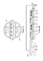
Referring first to FIGS. 1A and 1B , a carrier 101 having a plurality of first integrated circuit (IC) dies 107 and a plurality of second IC dies 109 attached thereon is illustrated in accordance with some embodiments. In some embodiments, a release layer 103 is formed over the carrier 101, an adhesive layer 105 is formed over the release layer 103, and the first IC dies 107 and the second IC dies 109 are attached to the adhesive layer 105. In some embodiments, the carrier 101 may be formed of silicon, quartz, glass, or the like, and provides mechanical support for subsequent operations. In some embodiments, the release layer 103 may comprise a light to heat conversion (LTHC) material, a ultraviolet (UV) glue (which loses its adhesive property when exposed to UV radiation), or the like, and may be formed using a spin-on coating process, a printing process, a lamination process, or the like. In some embodiments in which the release layer 103 is formed of an LTHC material, the release layer 103 partially or fully loses its adhesive strength when exposed to light and the carrier 101 can be easily detached from the first IC dies 107 and the second IC dies 109. The adhesive layer 105 may be a die attach film (DAF) or any suitable adhesive, epoxy, UV glue, or the like, and may be formed using a spin-on coating process, a printing process, a lamination process, or the like. In some embodiments, the first IC dies 107 and the second IC dies 109 are attached to the carrier 101 using, for example, a pick and place apparatus. In other embodiments, the first IC dies 107 and the second IC dies 109 may be attached to the carrier 101 manually, or using any other suitable method.
In some embodiments, the first IC dies 107 and the second IC dies 109 may be complementary metal-oxide-semiconductor (CMOS) dies, micro-electro-mechanical systems (MEMS) dies, or the like. The first IC dies 107 and the second IC dies 109 may have variety of functionalities and may include memory dies, microcontroller unit (MCU) chips, power management integrated circuit (PMIC) chips, radio frequency (RF) chips, application-specific integrated circuit (ASIC) chips, liquid crystal displays (LCDs), light emitting diode (LED) displays, touch sensors, motion sensors, heart rate sensors, ambient sensors such as temperature sensors, pressure sensors, humidity sensors, particle sensors, and the like. In some embodiments, the first IC dies 107 and the second IC dies 109 may be formed as part of a wafer, which is subsequently singulated into individual first IC dies 107 and individual second IC dies 109. In some embodiments, the wafer is singulated by sawing, laser ablation, or the like. Subsequently, functional testing may be performed on the first IC dies 107 and the second IC dies 109. Thus, the first IC dies 107 and the second IC dies 109 illustrated in FIGS. 1A and 1B may include only known good dies (KGDs), which have passed one or more functional quality tests. In the illustrated embodiment, the first IC dies 107 are CMOS dies and the second IC dies 109 are MEMS dies. In other embodiments, the first IC dies 107 and the second IC dies 109 may be MEMS dies. In yet other embodiments, the first IC dies 107 and the second IC dies 109 may be CMOS dies. Furthermore, as illustrated in FIG. 1B , top sides of the first IC dies 107 and the second IC dies 109 have different contact pad structures. However, in other embodiments, the first IC dies 107 and the second IC dies 109 have similar contact pad structures.
Referring further to FIGS. 1A and 1B , in some embodiments in which the first IC dies 107 are CMOS dies, each of the first IC dies 107 comprises a substrate 111, one or more active and/or passive devices 113 on the substrate 111, and one or more metallization layers 115 over the substrate 111 and the one or more active and/or passive devices 113. In some embodiments, the substrate 111 may be formed of silicon, although it may also be formed of other group III, group IV, and/or group V elements, such as silicon, germanium, gallium, arsenic, and combinations thereof. The substrate 111 may also be in the form of silicon-on-insulator (SOI). The SOI substrate may comprise a layer of a semiconductor material (e.g., silicon, germanium and/or the like) formed over an insulator layer (e.g., buried oxide and/or the like), which is formed on a silicon substrate. In addition, other substrates that may be used include multi-layered substrates, gradient substrates, hybrid orientation substrates, any combinations thereof and/or the like.
In some embodiments, the one or more active and/or passive devices 113 may include various n-type metal-oxide semiconductor (NMOS) and/or p-type metal-oxide semiconductor (PMOS) devices such as transistors, capacitors, resistors, diodes, photo-diodes, fuses and/or the like. The one or more metallization layers 115 may include an inter-layer dielectric (ILD)/inter-metal dielectric layers (IMDs) and conductive layers (not shown) separated by neighboring ILD/IMDs formed over the substrate 111. The ILD/IMDs may be formed, for example, of a low-K dielectric material, such as phosphosilicate glass (PSG), borophosphosilicate glass (BPSG), FSG, SiOxCy, Spin-On-Glass, Spin-On-Polymers, silicon carbon material, compounds thereof, composites thereof, combinations thereof, or the like, by any suitable method known in the art, such as a spin-on coating method, chemical vapor deposition (CVD), plasma enhanced CVD (PECVD), the like, or a combination thereof. In some embodiments, interconnect structures may be formed in the ILD/IMDs using, for example, a damascene process, a dual damascene process, or the like. In some embodiments, interconnect structures may comprise copper, a copper alloy, silver, gold, tungsten, tantalum, aluminum, or the like. In some embodiments, the interconnect structures may provide electrical connections between the one or more active and/or passive devices 113 formed on the substrate 111.
In some embodiments, each of the first IC dies 107 further includes contact pads 117 formed over the one or more metallization layers 115 and may be electrically coupled to the one or more active and/or passive devices 113 through various interconnect structures of the one or more metallization layers 115. In some embodiments, the contact pads 117 may comprise a conductive material such as aluminum, copper, tungsten, silver, gold, nickel, the like, or a combination thereof. In some embodiments, a conductive material may be formed over the one or more metallization layers 115 using, for example, physical vapor deposition (PVD), atomic layer deposition (ALD), electro-chemical plating, electroless plating, the like, or a combination thereof. In some embodiments in which the conductive material is aluminum, the conductive material is patterned to form the contact pads 117. In some embodiments, the conductive material may be patterned using photolithography techniques. Generally, photolithography techniques involve depositing a photoresist material (not shown), which is subsequently irradiated (exposed) and developed to remove a portion of the photoresist material. The remaining photoresist material protects the underlying material, such as the conductive material of the contact pads 117 from subsequent processing steps, such as etching. A suitable etching process, such as a reactive ion etch (RIE) or other dry etch, an isotropic or anisotropic wet etch, or any other suitable etch or patterning process may be applied to the conductive material to remove exposed portions of the conductive material and form the contact pads 117. In some embodiments in which the conductive material is aluminum, the conductive material may be etched using a mixture of 80% phosphoric acid, 5% nitric acid, 5% acetic acid, and 10% de-ionized (DI) water. Subsequently, the photoresist material may be removed using, for example, an ashing process followed by a wet clean process.
Referring further to FIGS. 1A and 1B , a passivation layer 119 is formed over the substrate 111 and the contact pads 117. In some embodiments, the passivation layer 119 may comprise one or more layers of photo-patternable dielectric materials such as polybenzoxazole (PBO), polyimide (PI), benzocyclobutene (BCB), or the like, and may be formed using a spin-on coating process, or the like. Such photo-patternable dielectric materials may be easily patterned using similar photolithography methods as a photoresist material. In other embodiments, the passivation layer 119 may comprise one or more layers of non-photo-patternable dielectric materials such as silicon nitride, silicon oxide, silicon oxynitride, phosphosilicate glass (PSG), borosilicate glass (BSG), boron-doped phosphosilicate glass (BPSG), or the like, and may be formed using CVD, PVD, ALD, a spin-on coating process, the like, or a combination thereof.
In some embodiments, openings 121 are formed in the passivation layer 119 to expose the contact pads 117. In some embodiments in which the passivation layer 119 is formed of a photo-patternable dielectric material, the passivation layer 119 may be patterned using similar photolithography methods as a photoresist material. In other embodiments in which the passivation layer 119 is formed of a non-photo-patternable dielectric material, a photoresist material (not shown) is formed over the passivation layer 119. The photoresist material is subsequently irradiated (exposed) and developed to remove a portion of the photoresist material. Subsequently, exposed portions of the passivation layer 119 are removed using, for example, a suitable etching process to form the openings 121. In some embodiments in which the passivation layer 119 is formed of silicon oxide, the passivation layer 119 is etched using, for example, buffered hydrofluoric acid (HF). In some embodiments in which the passivation layer 119 is formed of silicon nitride, the passivation layer 119 is etched using, for example, hot phosphoric acid (H3PO4). Subsequently, the photoresist material may be removed using, for example, an ashing process followed by a wet clean process.
Referring further to FIGS. 1A and 1B , in some embodiments in which the second IC dies 109 are MEMS dies, each of the second IC dies 109 comprises a MEMS substrate 123 bonded to a cap 125 and enclosing one or more cavities 127. In some embodiments, the MEMS substrate 123 and the cap 125 are bonded such that a front side 125A of the cap 125 faces a front side 123A of the MEMS substrate 123. The MEMS substrate 123 may be bonded to the cap 125 using any suitable technique such as fusion bonding (e.g., oxide-to-oxide bonding, metal-to-metal bonding, hybrid bonding, etc.), anodic bonding, eutectic bonding, the like, or a combination thereof. In some embodiments, the one or more cavities 127 may have a low pressure (high vacuum) as the bonding process may be performed in a low-pressure environment. In other embodiments, the one or more cavities 127 may have any suitable pressure depending on design requirements of the second IC dies 109.
In some embodiments, the MEMS substrate 123 may be formed using similar materials and methods as the substrate 111 and the description is not repeated herein. In some embodiments, each of the second IC dies 109 further includes various MEMS devices 129 on the front side 123A of the MEMS substrate 123 in the one or more cavities 127. The various MEMS devices 129 may include membranes, resonators, cantilevered elements, pressure sensors, accelerometers, motion sensors, gyroscopes, and the like and may be formed using suitable MEMS techniques. In some embodiments, the cap 125 may be a CMOS die and may be formed using similar materials and methods as the first IC dies 107. In other embodiments, the cap 125 may be a passive cap and may not have electrical circuits therein. In such embodiments, the cap 125 may be formed of a ceramic material, quartz, glass, or the like. The cap 125 may further include through vias (TVs) 131 extending from the front side 125A of the cap 125 to a backside 125B of the cap 125. The TVs 131 are configured to provide electrical connections between the various MEMS devices 129 and a circuitry that is external to the second IC dies 109. In the illustrated embodiment, the cap 125 further includes liner layers 133 along sidewalls of the TVs 131, a passivation layer 135 on the backside 125B of the cap 125 and contact pads 137 over the passivation layer 135 and contacting the TVs 131. In some embodiments, the liner layers 133 may comprise a suitable dielectric material and are configured to electrically isolate the TVs 131 from a material of the cap 125. In some embodiments, the TVs 131 and the contact pads 137 may comprise a conductive material such as aluminum, copper, tungsten, silver, gold, nickel, the like, or a combination thereof. In the illustrated embodiment, the TVs 131 and the contact pads 137 are formed of copper. In some embodiments, the passivation layer 135 may comprise one or more layers of silicon nitride, silicon oxide, silicon oxynitride, PSG, BSG, BPSG, or the like. Various processing steps during fabrication of the TVs 131 and the contact pads 137 are described below with reference to FIGS. 12-15 .
Referring further to FIGS. 1A and 1B , the first IC dies 107 and the second IC dies 109 have different contact pad structures. In the illustrated embodiment, the contact pad structure of the first IC dies 107 include the contact pads 117 embedded in the passivation layer 119, and the contact pad structure of the second IC dies 109 include the contact pads 137 over the passivation layer 135 and in electrical contact with TVs 131. As described below in greater detail, an encapsulant will be formed over the carrier 101 and between the first IC dies 107 and the second IC dies 109. Subsequently, one or more redistribution layers (RDLs) will be formed over the first IC dies 107, the second IC dies 109, and the encapsulant.
Referring first to FIGS. 2A and 2B , the molding tool 201 attaches a release layer 205 to the first IC dies 107 and the second IC dies 109. In some embodiments, the release layer 205 may be formed of a similar material as the release layer 103 and may be laminated on top surfaces of the first IC dies 107 and the second IC dies 109. In some embodiments, the molding tool 201 includes a plunger 203, which is configured to move in a lateral direction and transfer or inject the encapsulant 207 between the release layer 205 and the carrier 101, and in the gaps between the first IC dies 107 and the second IC dies 109.
Referring to FIG. 5 , after the encapsulation process is completed, the release layer 205 is removed and the top surfaces of the first IC dies 107 and the second IC dies 109 are exposed. By forming the encapsulant 207 using a method described above with reference to FIGS. 2A, 2B, 3A, 3B, 4A and 4B , the contact pads 117 of the first IC dies 107 and the contact pads 137 of the second IC dies 109 are not covered by the encapsulant 207 and are exposed after the release layer 205 is removed. As the encapsulant 207 is not covering the contact pads 117 of the first IC dies 107 and the contact pads 137 of the second IC dies 109, an encapsulant removal process such as a grinding process, a chemical mechanical polishing (CMP) process, or the like may be eliminated. Accordingly, top surfaces of the contact pads 117 and 137 may not be coplanar with a top surface 207A of the encapsulant 207. Furthermore, by forming the encapsulant 207 using a method described above with reference to FIGS. 2A, 2B, 3A, 3B, 4A and 4B , integrated circuit dies (such as the first IC dies 107 and the second IC dies 109) having different contact pad structures may be encapsulated without damaging the contact pad structures during the encapsulation process.
Referring to FIG. 6 , one or more redistribution layers (RDLs) 601 are formed over the first IC dies 107, the second IC dies 109, and the encapsulant 207 and are electrically coupled to the contact pads 117 of the first IC dies 107 and the contact pads 137 of the second IC dies 109. In some embodiments, the RDLs 601 comprise one or more dielectric layers 603 and one or more conductive features 605 (such as conductive lines or traces and vias) disposed within the one or more dielectric layers 603. In some embodiments, the one or more dielectric layers 603 may comprise dielectric materials such as PBO, PI, BCB, or the like, and may be formed using a spin-on coating process, or the like. In some embodiments, the one or more conductive features 605 may comprise copper, tungsten, aluminum, silver, gold, the like, or a combination thereof, may be formed using an electro-chemical plating process, an electroless plating process, ALD, PVD, the like, or a combination thereof.
Referring further to FIG. 6 , underbump metallizations (UBMs) 607 are formed over and electrically coupled to the one or more RDLs 601. In some embodiments, the UBMs 607 may include three layers of conductive materials, such as a layer of titanium, a layer of copper, and a layer of nickel. However, one of ordinary skill in the art will recognize that there are many suitable arrangements of materials and layers, such as an arrangement of chrome/chrome-copper alloy/copper/gold, an arrangement of titanium/titanium tungsten/copper, or an arrangement of copper/nickel/gold, that are suitable for the formation of the UBMs 607. Any suitable materials or layers of materials that may be used for the UBMs 607 are fully intended to be included within the scope of the current application.
Referring to FIG. 7 , connectors 701 are formed over and are electrically coupled to the UBMs 607. In some embodiments, the connectors 701 may be solder balls, metal pillars, controlled collapse chip connection (C4) bumps, ball grid array (BGA) balls, micro bumps, electroless nickel-electroless palladium-immersion gold technique (ENEPIG) formed bumps, or the like. The connectors 701 may include a conductive material such as solder, copper, aluminum, gold, nickel, silver, palladium, tin, the like, or a combination thereof. In some embodiments in which the connectors 701 are solder bumps, the connectors 701 may be formed by initially forming a layer of solder through commonly used methods such as evaporation, electroplating, printing, solder transfer, ball placement, or the like. Once the layer of solder has been formed on the structure, a reflow may be performed in order to shape the material into the desired bump shapes. In other embodiments, the connectors 701 may be metal pillars (such as, for example, copper pillars) formed by a sputtering, printing, electro-chemical plating, electroless plating, PVD, or the like. The metal pillars may be solder free and have substantially vertical sidewalls. In some embodiments, a metal cap layer (not shown) is formed on the top of the metal pillars. The metal cap layer may include a solder, nickel, tin, tin-lead, gold, silver, palladium, indium, nickel-palladium-gold, nickel-gold, the like, or a combination thereof and may be formed by a plating process, or the like.
Referring further to FIG. 7 , the carrier 101 is removed from encapsulated first IC dies 107 and second IC dies 109 and the encapsulated first IC dies 107 and second IC dies 109 is diced to form individual integrated circuit packages 703. In some embodiments in which the release layer 103 is formed of an LTHC material, the release layer 103 is exposed to light. The exposure to light causes the release layer 103 to lose its adhesive strength and the carrier 101 is easily detached from the first IC dies 107, the second IC dies 109 and the encapsulant 207. Subsequently, the adhesive layer 105 may be removed to expose the first IC dies 107, the second IC dies 109 and the encapsulant 207. In some embodiments, the encapsulated first IC dies 107 and second IC dies 109 may be diced using, for example, etching, sawing, laser ablation, the like, or a combination thereof. Subsequently, each of the IC packages 703 may be tested to identify known good packages (KGPs) for further processing.
Referring further to FIG. 12 , a liner layer 133 is conformally formed over the front side 125A of the cap 125 and in the openings. In some embodiments, the liner layer 133 may comprise a suitable dielectric material and may be formed using CVD, PECVD, sub atmospheric CVD (SACVD), ALD, the like, or combination thereof. The liner layer 133 is configured to electrically isolate subsequently formed TVs 131 from a material of the cap 125. In some embodiments, a barrier/adhesion layer (not shown) is conformally formed over the liner layer 133. The barrier/adhesion layer may be formed using sputtering, PVD, CVD, ALD, the like or a combination thereof. The barrier/adhesion layer is configured to act a diffusion barrier and protect the cap 125 from metal diffusion. The TVs 131 are formed by filling the openings with a conductive material such as aluminum, copper, tungsten, silver, gold, the like, or a combination thereof. In some embodiment, the conductive material is deposited using an electro-chemical plating process, an electroless plating process, ALD, PVD, the like, or a combination thereof. In some embodiments, before filling the openings with the conductive material, a seed layer (not shown) is conformally formed over the barrier/adhesion layer, and the conductive material is deposited over the seed layer. The seed layer may comprise copper, titanium, nickel, gold, manganese, the like, or a combination thereof, and may be formed by ALD, PVD, sputtering, the like, or a combination thereof. In some embodiments, the openings on the front side 125A of the cap 125 are over-filled with the conductive material, which may be removed using an etch process, a CMP process, or the like. After forming the TVs 131 in the cap 125, the cap 125 and the MEMS substrate 123 are boded to form the wafer 1200 having the second IC dies 109. The MEMS substrate 123 may be bonded to the cap 125 using any suitable technique such as fusion bonding (e.g., oxide-to-oxide bonding, metal-to-metal bonding, hybrid bonding, etc.), anodic bonding, eutectic bonding, the like, or a combination thereof.
Referring to FIG. 13 , the backside 125B of the cap 125 is thinned until the TVs 131 are exposed. In some embodiments, the backside 125B of the cap 125 may be thinned using a grinding process, an etching process, a CMP process, or the like. In some embodiments, the process continues to form contact pads 137 over the backside 125B of the cap 125 and in electrical contact with the TVs 121 as described in greater detail below with reference to FIGS. 14 and 15 . In other embodiments, the process stops here and the wafer 1200 may be singulated along the scribe line 1201 before forming contact pads 137. In such embodiments, individual dies such as the IC die 903 illustrated in FIGS. 9A and 9B may be formed.
Referring to FIG. 14 , a passivation layer 135 is formed on the backside 125B of the cap 125 and over the TVs 131. In some embodiments, the passivation layer 135 may comprise one or more layers of silicon nitride, silicon oxide, silicon oxynitride, PSG, BSG, BPSG, or the like, and may be formed using CVD, PVD, ALD, a spin-on coating process, the like, or a combination thereof. In some embodiments, the passivation layer 135 is planarized until TVs 131 are exposed. In some embodiments, the passivation layer 135 may be planarized using a grinding process, an etching process, a CMP process, or the like. Subsequently, the passivation layer 135 is recessed to expose at least portion of a sidewall of the TVs 131 and form via protrusions extending above a top surface of the passivation layer 135. In some embodiments, the passivation layer 135 may be recessed using a selective etching process, or the like.
Referring to FIG. 15 , contact pads 137 are formed over the passivation layer 135 and in electrical contact with TVs 131. In some embodiments, a sacrificial layer (not shown) may be formed over the passivation layer 135 and patterned to form openings in the sacrificial layer. In some embodiments, the sacrificial layer may comprise a photoresist material, or the like. The openings in the sacrificial layer expose the via protrusions of the TVs 131. In some embodiments, a conductive material such as aluminum, copper, tungsten, silver, gold, nickel, the like, or a combination thereof is deposited in the openings in the sacrificial layer to form the contact pads 137. In other embodiments, a conductive material may be formed over the passivation layer and subsequently patterned to form the contact pads. After completing the formation of the contact pads 137, the wafer 1200 is diced to form individual second IC dies 109. In some embodiments, the wafer may be diced using, for example, etching, sawing, laser ablation, the like, or a combination thereof. Subsequently, each of the second IC dies 109 may be tested to identify known good packages (KGPs) for further processing.
Various embodiments presented herein may provide several advantages. Embodiments such as described herein allow for packaging integrated circuit dies having different contact pad structures into a same integrated circuit package. Furthermore, embodiments such as described herein allow for eliminating certain process steps and allow for reducing manufacturing costs during formation of integrated circuit package. In addition, embodiments such a described herein allow for encapsulation of integrated circuit dies having different contact pad structures without damaging the contact pad structures during the encapsulation process.
In accordance with an embodiment, a method includes attaching a first die and a second die to a carrier, the first die having a first contact pad, the second die having a second contact pad, the first contact pad and the second contact pad having different structures. A release layer is formed over the first die and the second die. An encapsulant is injected between the carrier and the release layer. One or more redistribution layers (RDLs) are formed over the first die, the second die and the encapsulant, the first contact pad and the second contact pad being in electrical contact with the one or more RDLs.
In accordance with another embodiment, a method includes attaching a first side of a first die to a carrier. The first die includes a first contact pad on a second side of the first die, the second side of the first die being opposite the first side of the first die. The first die further includes a first insulating layer on the second side of the first die, at least a portion of the first contact pad being exposed through an opening in the first insulating layer. A first side of a second die is attached to the carrier. The second die includes a through via, the through via extending from the first side of the second die to a second side of the second die, the second side of the second die being opposite the first side of the second die. The second die further includes a second insulating layer on the second side of the second die, at least a portion of the through via extending through the second insulating layer, and a second contact pad over the second insulating layer, the second contact pad contacting the through via. A release layer is laminated over top surfaces of the first contact pad, the second contact pad, the first insulating layer and the second insulating layer. A first encapsulant is injected between the carrier and the release layer, and in a gap between the first die and the second die. One or more redistribution layers (RDLs) are formed over the first die, the second die and the first encapsulant, the first contact pad and the second contact pad being in electrical contact with the one or more RDLs.
In accordance with yet another embodiment, a device includes one or more redistribution layers (RDLs), and a first die on a first side of the one or more RDLs, the first die comprising a first contact pad embedded in a first insulating layer, a conductive feature of the one or more RDLs extending through the first insulating layer and contacting the first contact pad. The device further includes a second die on the first side of the one or more RDLs. The second die includes a through via extending through a second insulating layer, and a second contact pad over the second insulating layer, the second contact pad contacting the through via, at least a portion of a third insulating layer of the one or more RDLs extending along a sidewall of the second contact pad. The device further includes a first encapsulant on the first side of the one or more RDLs, at least a portion of the first encapsulant being interposed between the first die and the second die.
The foregoing outlines features of several embodiments so that those skilled in the art may better understand the aspects of the present disclosure. Those skilled in the art should appreciate that they may readily use the present disclosure as a basis for designing or modifying other processes and structures for carrying out the same purposes and/or achieving the same advantages of the embodiments introduced herein. Those skilled in the art should also realize that such equivalent constructions do not depart from the spirit and scope of the present disclosure, and that they may make various changes, substitutions, and alterations herein without departing from the spirit and scope of the present disclosure.
Claims (20)
1. A device comprising:
one or more redistribution layers (RDLs);
a first die on a first side of the one or more RDLs, the first die comprising a first contact pad embedded in a first insulating layer, a conductive feature of the one or more RDLs extending through the first insulating layer and contacting the first contact pad;
a second die on the first side of the one or more RDLs, the second die comprising:
a through via extending through a second insulating layer; and
a second contact pad over the second insulating layer, the second contact pad contacting the through via, at least a portion of a third insulating layer of the one or more RDLs extending along a sidewall of the second contact pad; and
a first encapsulant on the first side of the one or more RDLs, at least a portion of the first encapsulant being interposed between the first die and the second die.
2. The device of claim 1 , further comprising:
a third die on a second side of the one or more RDLs, the second side of the one or more RDLs being opposite the first side of the one or more RDLs;
a second encapsulant on the second side of the one or more RDLs, the third die extending through the second encapsulant; and
a circuit board on the second side of the one or more RDLs, the second encapsulant extending through an opening in the circuit board.
3. The device of claim 2 , wherein at least a portion of the second encapsulant is interposed between the third die and the one or more RDLs.
4. The device of claim 1 , wherein a topmost surface of the first encapsulant is below a topmost surface of the first insulating layer.
5. The device of claim 4 , wherein the topmost surface of the first encapsulant is below a topmost surface of the second contact pad.
6. The device of claim 1 , wherein the first encapsulant extends over a major surface of the second die, the second die being interposed between the first encapsulant and the one or more redistribution layers.
7. The device of claim 6 , wherein a portion of the major surface is exposed through the first encapsulant.
8. A device comprising:
a first die, the first die having a first contact and a first dielectric layer, the first dielectric layer covering at least a portion of the first contact;
a second die, the second die having a second contact, the first contact having a different topography than the second contact;
a molding compound interposed between the first die and the second die; and
a first redistribution structure extending over the first die, the second die, and the molding compound, the first redistribution structure comprising a second dielectric layer, the second dielectric layer extending along sidewalls of the second contact, sidewalls of the first contact being free of the second dielectric layer.
9. The device of claim 8 , wherein the second die comprises through via and a passivation layer, the passivation layer having a tapered section adjacent the through via.
10. The device of claim 9 , wherein the second die further comprises a contact pad over the through via, the contact pad extending over the tapered section.
11. The device of claim 10 , wherein at least a portion of the tapered section of the passivation layer is interposed between the contact pad and the through via.
12. The device of claim 8 , wherein the second die comprises a first surface and a second surface, the first surface being interposed between the second surface and the first redistribution structure, the molding compound extending along a portion of the second surface of the second die.
13. The device of claim 12 , wherein the second die is a MEMS device, and wherein at least a portion of the second surface of the second die is exposed through the molding compound.
14. The device of claim 8 , wherein the first redistribution structure is directly coupled to a board, wherein the first redistribution structure is interposed between the board and the first die.
15. The device of claim 14 , further comprising a third die, the third die being directly coupled to the first redistribution structure.
16. A device comprising:
a first die, the first die having a first contact and a first dielectric layer, the first dielectric layer covering at least a portion of the first contact;
a second die, the second die having a second contact on a first surface;
a molding compound interposed between the first die and the second die; and
a first redistribution structure extending over the first die, the second die, and the molding compound, the first redistribution structure comprising a second dielectric layer, the second dielectric layer extending along sidewalls of the second contact and at least a portion of a major surface of the second contact, the first redistribution structure comprising a first conductive element and a second conductive element, the first conductive element extending through the first dielectric layer and the second dielectric layer to the first contact, the second conductive element extending through the second dielectric layer to the second contact.
17. The device of claim 16 , wherein the second contact comprises a through via protruding from a surface of the second die.
18. The device of claim 17 , further comprising a pad interposed between the through via and the second conductive element of the first redistribution structure.
19. The device of claim 16 , wherein the molding compound covers at least a portion of a second surface of the second die.
20. The device of claim 19 , further comprising:
a printed circuit board coupled to the first redistribution structure; and
a third die coupled to the first redistribution structure, the first redistribution structure being interposed between the first die and the third die.
Priority Applications (1)
| Application Number | Priority Date | Filing Date | Title |
|---|---|---|---|
| US15/843,372 US10125014B2 (en) | 2015-12-31 | 2017-12-15 | Integrated circuit package and method of forming same |
Applications Claiming Priority (2)
| Application Number | Priority Date | Filing Date | Title |
|---|---|---|---|
| US14/986,189 US9850126B2 (en) | 2015-12-31 | 2015-12-31 | Integrated circuit package and method of forming same |
| US15/843,372 US10125014B2 (en) | 2015-12-31 | 2017-12-15 | Integrated circuit package and method of forming same |
Related Parent Applications (1)
| Application Number | Title | Priority Date | Filing Date |
|---|---|---|---|
| US14/986,189 Division US9850126B2 (en) | 2015-12-31 | 2015-12-31 | Integrated circuit package and method of forming same |
Publications (2)
| Publication Number | Publication Date |
|---|---|
| US20180111827A1 US20180111827A1 (en) | 2018-04-26 |
| US10125014B2 true US10125014B2 (en) | 2018-11-13 |
Family
ID=59227059
Family Applications (2)
| Application Number | Title | Priority Date | Filing Date |
|---|---|---|---|
| US14/986,189 Active US9850126B2 (en) | 2015-12-31 | 2015-12-31 | Integrated circuit package and method of forming same |
| US15/843,372 Active US10125014B2 (en) | 2015-12-31 | 2017-12-15 | Integrated circuit package and method of forming same |
Family Applications Before (1)
| Application Number | Title | Priority Date | Filing Date |
|---|---|---|---|
| US14/986,189 Active US9850126B2 (en) | 2015-12-31 | 2015-12-31 | Integrated circuit package and method of forming same |
Country Status (3)
| Country | Link |
|---|---|
| US (2) | US9850126B2 (en) |
| CN (1) | CN106997855A (en) |
| TW (1) | TW201724418A (en) |
Families Citing this family (43)
| Publication number | Priority date | Publication date | Assignee | Title |
|---|---|---|---|---|
| US8832283B1 (en) * | 2010-09-16 | 2014-09-09 | Google Inc. | Content provided DNS resolution validation and use |
| US9583414B2 (en) | 2013-10-31 | 2017-02-28 | Qorvo Us, Inc. | Silicon-on-plastic semiconductor device and method of making the same |
| US9812350B2 (en) | 2013-03-06 | 2017-11-07 | Qorvo Us, Inc. | Method of manufacture for a silicon-on-plastic semiconductor device with interfacial adhesion layer |
| US10085352B2 (en) | 2014-10-01 | 2018-09-25 | Qorvo Us, Inc. | Method for manufacturing an integrated circuit package |
| US9530709B2 (en) | 2014-11-03 | 2016-12-27 | Qorvo Us, Inc. | Methods of manufacturing a printed circuit module having a semiconductor device with a protective layer in place of a low-resistivity handle layer |
| US9613831B2 (en) | 2015-03-25 | 2017-04-04 | Qorvo Us, Inc. | Encapsulated dies with enhanced thermal performance |
| US9960145B2 (en) | 2015-03-25 | 2018-05-01 | Qorvo Us, Inc. | Flip chip module with enhanced properties |
| US20160343604A1 (en) | 2015-05-22 | 2016-11-24 | Rf Micro Devices, Inc. | Substrate structure with embedded layer for post-processing silicon handle elimination |
| US10276495B2 (en) | 2015-09-11 | 2019-04-30 | Qorvo Us, Inc. | Backside semiconductor die trimming |
| US10020405B2 (en) | 2016-01-19 | 2018-07-10 | Qorvo Us, Inc. | Microelectronics package with integrated sensors |
| US10062583B2 (en) | 2016-05-09 | 2018-08-28 | Qorvo Us, Inc. | Microelectronics package with inductive element and magnetically enhanced mold compound component |
| US10784149B2 (en) | 2016-05-20 | 2020-09-22 | Qorvo Us, Inc. | Air-cavity module with enhanced device isolation |
| US10773952B2 (en) | 2016-05-20 | 2020-09-15 | Qorvo Us, Inc. | Wafer-level package with enhanced performance |
| US10103080B2 (en) | 2016-06-10 | 2018-10-16 | Qorvo Us, Inc. | Thermally enhanced semiconductor package with thermal additive and process for making the same |
| US10079196B2 (en) | 2016-07-18 | 2018-09-18 | Qorvo Us, Inc. | Thermally enhanced semiconductor package having field effect transistors with back-gate feature |
| EP3497717A1 (en) | 2016-08-12 | 2019-06-19 | Qorvo Us, Inc. | Wafer-level package with enhanced performance |
| US10486963B2 (en) | 2016-08-12 | 2019-11-26 | Qorvo Us, Inc. | Wafer-level package with enhanced performance |
| WO2018031999A1 (en) * | 2016-08-12 | 2018-02-15 | Qorvo Us, Inc. | Wafer-level package with enhanced performance |
| US10109502B2 (en) | 2016-09-12 | 2018-10-23 | Qorvo Us, Inc. | Semiconductor package with reduced parasitic coupling effects and process for making the same |
| US10090339B2 (en) | 2016-10-21 | 2018-10-02 | Qorvo Us, Inc. | Radio frequency (RF) switch |
| US10749518B2 (en) | 2016-11-18 | 2020-08-18 | Qorvo Us, Inc. | Stacked field-effect transistor switch |
| US10068831B2 (en) | 2016-12-09 | 2018-09-04 | Qorvo Us, Inc. | Thermally enhanced semiconductor package and process for making the same |
| US10755992B2 (en) | 2017-07-06 | 2020-08-25 | Qorvo Us, Inc. | Wafer-level packaging for enhanced performance |
| US10784233B2 (en) | 2017-09-05 | 2020-09-22 | Qorvo Us, Inc. | Microelectronics package with self-aligned stacked-die assembly |
| US10366972B2 (en) | 2017-09-05 | 2019-07-30 | Qorvo Us, Inc. | Microelectronics package with self-aligned stacked-die assembly |
| US11152363B2 (en) | 2018-03-28 | 2021-10-19 | Qorvo Us, Inc. | Bulk CMOS devices with enhanced performance and methods of forming the same utilizing bulk CMOS process |
| US20190326232A1 (en) * | 2018-04-23 | 2019-10-24 | Wei-Cheng Lin | Receiver and transmitter chips packaging structure and automotive radar detector device using same |
| US10804246B2 (en) | 2018-06-11 | 2020-10-13 | Qorvo Us, Inc. | Microelectronics package with vertically stacked dies |
| US10964554B2 (en) | 2018-10-10 | 2021-03-30 | Qorvo Us, Inc. | Wafer-level fan-out package with enhanced performance |
| US11069590B2 (en) | 2018-10-10 | 2021-07-20 | Qorvo Us, Inc. | Wafer-level fan-out package with enhanced performance |
| US11646242B2 (en) | 2018-11-29 | 2023-05-09 | Qorvo Us, Inc. | Thermally enhanced semiconductor package with at least one heat extractor and process for making the same |
| CN111377391B (en) * | 2018-12-27 | 2023-08-25 | 中芯集成电路(宁波)有限公司上海分公司 | MEMS packaging structure and manufacturing method thereof |
| EP3915134A1 (en) | 2019-01-23 | 2021-12-01 | Qorvo US, Inc. | Rf semiconductor device and manufacturing method thereof |
| US20200235066A1 (en) | 2019-01-23 | 2020-07-23 | Qorvo Us, Inc. | Rf devices with enhanced performance and methods of forming the same |
| US11387157B2 (en) | 2019-01-23 | 2022-07-12 | Qorvo Us, Inc. | RF devices with enhanced performance and methods of forming the same |
| US20200235040A1 (en) | 2019-01-23 | 2020-07-23 | Qorvo Us, Inc. | Rf devices with enhanced performance and methods of forming the same |
| US11610846B2 (en) * | 2019-04-12 | 2023-03-21 | Adeia Semiconductor Bonding Technologies Inc. | Protective elements for bonded structures including an obstructive element |
| US10950551B2 (en) * | 2019-04-29 | 2021-03-16 | Advanced Semiconductor Engineering, Inc. | Embedded component package structure and manufacturing method thereof |
| US11296062B2 (en) * | 2019-06-25 | 2022-04-05 | Taiwan Semiconductor Manufacturing Company, Ltd. | Three-dimension large system integration |
| US10978338B1 (en) * | 2019-11-13 | 2021-04-13 | Nanya Technology Corporation | Semiconductor device and manufacture method thereof |
| US11646289B2 (en) | 2019-12-02 | 2023-05-09 | Qorvo Us, Inc. | RF devices with enhanced performance and methods of forming the same |
| US11923238B2 (en) | 2019-12-12 | 2024-03-05 | Qorvo Us, Inc. | Method of forming RF devices with enhanced performance including attaching a wafer to a support carrier by a bonding technique without any polymer adhesive |
| DE102020211741A1 (en) * | 2020-09-21 | 2022-03-24 | Robert Bosch Gesellschaft mit beschränkter Haftung | Micromechanical sensor |
Citations (23)
| Publication number | Priority date | Publication date | Assignee | Title |
|---|---|---|---|---|
| US7993941B2 (en) | 2008-12-05 | 2011-08-09 | Stats Chippac, Ltd. | Semiconductor package and method of forming Z-direction conductive posts embedded in structurally protective encapsulant |
| US8039304B2 (en) * | 2009-08-12 | 2011-10-18 | Stats Chippac, Ltd. | Semiconductor device and method of dual-molding die formed on opposite sides of build-up interconnect structures |
| US20110291288A1 (en) | 2010-05-26 | 2011-12-01 | Taiwan Semiconductor Manufacturing Company, Ltd. | Package systems having interposers |
| US8361842B2 (en) | 2010-07-30 | 2013-01-29 | Taiwan Semiconductor Manufacturing Company, Ltd. | Embedded wafer-level bonding approaches |
| US20130026468A1 (en) | 2010-04-07 | 2013-01-31 | Shimadzu Corporation | Radiation detector and method of manufacturing the same |
| US20130062760A1 (en) | 2010-10-14 | 2013-03-14 | Taiwan Semiconductor Manufacturing Company, Ltd. | Packaging Methods and Structures Using a Die Attach Film |
| US20130062761A1 (en) | 2011-09-09 | 2013-03-14 | Taiwan Semiconductor Manufacturing Company, Ltd. | Packaging Methods and Structures for Semiconductor Devices |
| US20130168848A1 (en) | 2011-12-28 | 2013-07-04 | Taiwan Semiconductor Manufacturing Company, Ltd. | Packaged semiconductor device and method of packaging the semiconductor device |
| US20130307140A1 (en) | 2012-05-18 | 2013-11-21 | Taiwan Semiconductor Manufacturing Company, Ltd. | Packaging with interposer frame |
| US8680647B2 (en) | 2011-12-29 | 2014-03-25 | Taiwan Semiconductor Manufacturing Company, Ltd. | Packages with passive devices and methods of forming the same |
| US8703542B2 (en) | 2012-05-18 | 2014-04-22 | Taiwan Semiconductor Manufacturing Company, Ltd. | Wafer-level packaging mechanisms |
| US8759964B2 (en) | 2007-07-17 | 2014-06-24 | Taiwan Semiconductor Manufacturing Company, Ltd. | Wafer level package structure and fabrication methods |
| US8778738B1 (en) | 2013-02-19 | 2014-07-15 | Taiwan Semiconductor Manufacturing Company, Ltd. | Packaged semiconductor devices and packaging devices and methods |
| US8785299B2 (en) | 2012-11-30 | 2014-07-22 | Taiwan Semiconductor Manufacturing Company, Ltd. | Package with a fan-out structure and method of forming the same |
| US20140203429A1 (en) | 2013-01-18 | 2014-07-24 | Taiwan Semiconductor Manufacturing Company, Ltd. | Fan-out package structure and methods for forming the same |
| US20140225222A1 (en) | 2013-02-11 | 2014-08-14 | Taiwan Semiconductor Manufacturing Company, Ltd. | Package with metal-insulator-metal capacitor and method of manufacturing the same |
| US8809996B2 (en) | 2012-06-29 | 2014-08-19 | Taiwan Semiconductor Manufacturing Company, Ltd. | Package with passive devices and method of forming the same |
| US8829676B2 (en) | 2011-06-28 | 2014-09-09 | Taiwan Semiconductor Manufacturing Company, Ltd. | Interconnect structure for wafer level package |
| US20140252646A1 (en) | 2013-03-06 | 2014-09-11 | Taiwan Semiconductor Manufacturing Company, Ltd. | Interconnect Structure for Package-on-Package Devices |
| US20140264930A1 (en) | 2013-03-15 | 2014-09-18 | Taiwan Semiconductor Manufacturing Company, Ltd. | Fan-Out Interconnect Structure and Method for Forming Same |
| US8877554B2 (en) | 2013-03-15 | 2014-11-04 | Taiwan Semiconductor Manufacturing Company, Ltd. | Packaged semiconductor devices, methods of packaging semiconductor devices, and PoP devices |
| US8916481B2 (en) | 2011-11-02 | 2014-12-23 | Stmicroelectronics Pte Ltd. | Embedded wafer level package for 3D and package-on-package applications, and method of manufacture |
| US9583472B2 (en) * | 2015-03-03 | 2017-02-28 | Apple Inc. | Fan out system in package and method for forming the same |
-
2015
- 2015-12-31 US US14/986,189 patent/US9850126B2/en active Active
-
2016
- 2016-11-23 TW TW105138499A patent/TW201724418A/en unknown
- 2016-12-27 CN CN201611222981.XA patent/CN106997855A/en active Pending
-
2017
- 2017-12-15 US US15/843,372 patent/US10125014B2/en active Active
Patent Citations (24)
| Publication number | Priority date | Publication date | Assignee | Title |
|---|---|---|---|---|
| US8759964B2 (en) | 2007-07-17 | 2014-06-24 | Taiwan Semiconductor Manufacturing Company, Ltd. | Wafer level package structure and fabrication methods |
| US7993941B2 (en) | 2008-12-05 | 2011-08-09 | Stats Chippac, Ltd. | Semiconductor package and method of forming Z-direction conductive posts embedded in structurally protective encapsulant |
| US8039304B2 (en) * | 2009-08-12 | 2011-10-18 | Stats Chippac, Ltd. | Semiconductor device and method of dual-molding die formed on opposite sides of build-up interconnect structures |
| US20130026468A1 (en) | 2010-04-07 | 2013-01-31 | Shimadzu Corporation | Radiation detector and method of manufacturing the same |
| US20110291288A1 (en) | 2010-05-26 | 2011-12-01 | Taiwan Semiconductor Manufacturing Company, Ltd. | Package systems having interposers |
| US8361842B2 (en) | 2010-07-30 | 2013-01-29 | Taiwan Semiconductor Manufacturing Company, Ltd. | Embedded wafer-level bonding approaches |
| US20130062760A1 (en) | 2010-10-14 | 2013-03-14 | Taiwan Semiconductor Manufacturing Company, Ltd. | Packaging Methods and Structures Using a Die Attach Film |
| US8829676B2 (en) | 2011-06-28 | 2014-09-09 | Taiwan Semiconductor Manufacturing Company, Ltd. | Interconnect structure for wafer level package |
| US20130062761A1 (en) | 2011-09-09 | 2013-03-14 | Taiwan Semiconductor Manufacturing Company, Ltd. | Packaging Methods and Structures for Semiconductor Devices |
| US8916481B2 (en) | 2011-11-02 | 2014-12-23 | Stmicroelectronics Pte Ltd. | Embedded wafer level package for 3D and package-on-package applications, and method of manufacture |
| US20130168848A1 (en) | 2011-12-28 | 2013-07-04 | Taiwan Semiconductor Manufacturing Company, Ltd. | Packaged semiconductor device and method of packaging the semiconductor device |
| US8680647B2 (en) | 2011-12-29 | 2014-03-25 | Taiwan Semiconductor Manufacturing Company, Ltd. | Packages with passive devices and methods of forming the same |
| US8703542B2 (en) | 2012-05-18 | 2014-04-22 | Taiwan Semiconductor Manufacturing Company, Ltd. | Wafer-level packaging mechanisms |
| US20130307140A1 (en) | 2012-05-18 | 2013-11-21 | Taiwan Semiconductor Manufacturing Company, Ltd. | Packaging with interposer frame |
| US8809996B2 (en) | 2012-06-29 | 2014-08-19 | Taiwan Semiconductor Manufacturing Company, Ltd. | Package with passive devices and method of forming the same |
| US8785299B2 (en) | 2012-11-30 | 2014-07-22 | Taiwan Semiconductor Manufacturing Company, Ltd. | Package with a fan-out structure and method of forming the same |
| US8803306B1 (en) | 2013-01-18 | 2014-08-12 | Taiwan Semiconductor Manufacturing Company, Ltd. | Fan-out package structure and methods for forming the same |
| US20140203429A1 (en) | 2013-01-18 | 2014-07-24 | Taiwan Semiconductor Manufacturing Company, Ltd. | Fan-out package structure and methods for forming the same |
| US20140225222A1 (en) | 2013-02-11 | 2014-08-14 | Taiwan Semiconductor Manufacturing Company, Ltd. | Package with metal-insulator-metal capacitor and method of manufacturing the same |
| US8778738B1 (en) | 2013-02-19 | 2014-07-15 | Taiwan Semiconductor Manufacturing Company, Ltd. | Packaged semiconductor devices and packaging devices and methods |
| US20140252646A1 (en) | 2013-03-06 | 2014-09-11 | Taiwan Semiconductor Manufacturing Company, Ltd. | Interconnect Structure for Package-on-Package Devices |
| US20140264930A1 (en) | 2013-03-15 | 2014-09-18 | Taiwan Semiconductor Manufacturing Company, Ltd. | Fan-Out Interconnect Structure and Method for Forming Same |
| US8877554B2 (en) | 2013-03-15 | 2014-11-04 | Taiwan Semiconductor Manufacturing Company, Ltd. | Packaged semiconductor devices, methods of packaging semiconductor devices, and PoP devices |
| US9583472B2 (en) * | 2015-03-03 | 2017-02-28 | Apple Inc. | Fan out system in package and method for forming the same |
Also Published As
| Publication number | Publication date |
|---|---|
| CN106997855A (en) | 2017-08-01 |
| TW201724418A (en) | 2017-07-01 |
| US20180111827A1 (en) | 2018-04-26 |
| US20170190572A1 (en) | 2017-07-06 |
| US9850126B2 (en) | 2017-12-26 |
Similar Documents
| Publication | Publication Date | Title |
|---|---|---|
| US10125014B2 (en) | Integrated circuit package and method of forming same | |
| US11443995B2 (en) | Integrated circuit package and method | |
| US20220301889A1 (en) | Integrated Circuit Packages and Methods of Forming Same | |
| US10510629B2 (en) | Integrated circuit package and method of forming same | |
| US10090284B2 (en) | Semiconductor device and method of manufacture | |
| US10529698B2 (en) | Semiconductor packages and methods of forming same | |
| US10854552B2 (en) | Semiconductor device and method of manufacture | |
| US9728522B2 (en) | Integrated circuit packages and methods of forming same | |
| US10163661B2 (en) | Stacked semiconductor devices and methods of forming same | |
| KR101823225B1 (en) | Package structures and method of forming the same | |
| US9209048B2 (en) | Two step molding grinding for packaging applications | |
| CN111799227B (en) | Semiconductor device and method of forming the same | |
| US11862605B2 (en) | Integrated circuit package and method of forming same | |
| US20170084544A1 (en) | Integrated Circuit Dies Having Alignment Marks and Methods of Forming Same | |
| US9455236B2 (en) | Integrated circuit packages and methods of forming same | |
| US11101260B2 (en) | Method of forming a dummy die of an integrated circuit having an embedded annular structure | |
| US9391028B1 (en) | Integrated circuit dies having alignment marks and methods of forming same | |
| US20230109128A1 (en) | Heat Dissipation in Semiconductor Packages and Methods of Forming Same | |
| US20220301970A1 (en) | Semiconductor package and method of manufacturing semiconductor package | |
| US11715646B2 (en) | Semiconductor structure and method for forming the same | |
| TW202230646A (en) | Semiconductor packages |
Legal Events
| Date | Code | Title | Description |
|---|---|---|---|
| FEPP | Fee payment procedure |
Free format text: ENTITY STATUS SET TO UNDISCOUNTED (ORIGINAL EVENT CODE: BIG.); ENTITY STATUS OF PATENT OWNER: LARGE ENTITY |
|
| STCF | Information on status: patent grant |
Free format text: PATENTED CASE |
|
| MAFP | Maintenance fee payment |
Free format text: PAYMENT OF MAINTENANCE FEE, 4TH YEAR, LARGE ENTITY (ORIGINAL EVENT CODE: M1551); ENTITY STATUS OF PATENT OWNER: LARGE ENTITY Year of fee payment: 4 |