US10115669B2 - High density nonvolatile memory cell unit array - Google Patents
High density nonvolatile memory cell unit array Download PDFInfo
- Publication number
- US10115669B2 US10115669B2 US15/509,575 US201515509575A US10115669B2 US 10115669 B2 US10115669 B2 US 10115669B2 US 201515509575 A US201515509575 A US 201515509575A US 10115669 B2 US10115669 B2 US 10115669B2
- Authority
- US
- United States
- Prior art keywords
- memory cell
- control circuit
- cell unit
- wires
- layer
- Prior art date
- Legal status (The legal status is an assumption and is not a legal conclusion. Google has not performed a legal analysis and makes no representation as to the accuracy of the status listed.)
- Expired - Fee Related
Links
Images


Classifications
-
- G—PHYSICS
- G11—INFORMATION STORAGE
- G11C—STATIC STORES
- G11C5/00—Details of stores covered by group G11C11/00
- G11C5/02—Disposition of storage elements, e.g. in the form of a matrix array
- G11C5/025—Geometric lay-out considerations of storage- and peripheral-blocks in a semiconductor storage device
-
- G—PHYSICS
- G11—INFORMATION STORAGE
- G11C—STATIC STORES
- G11C13/00—Digital stores characterised by the use of storage elements not covered by groups G11C11/00, G11C23/00, or G11C25/00
- G11C13/0002—Digital stores characterised by the use of storage elements not covered by groups G11C11/00, G11C23/00, or G11C25/00 using resistive RAM [RRAM] elements
- G11C13/0021—Auxiliary circuits
-
- H—ELECTRICITY
- H01—ELECTRIC ELEMENTS
- H01L—SEMICONDUCTOR DEVICES NOT COVERED BY CLASS H10
- H01L23/00—Details of semiconductor or other solid state devices
- H01L23/52—Arrangements for conducting electric current within the device in operation from one component to another, i.e. interconnections, e.g. wires, lead frames
- H01L23/522—Arrangements for conducting electric current within the device in operation from one component to another, i.e. interconnections, e.g. wires, lead frames including external interconnections consisting of a multilayer structure of conductive and insulating layers inseparably formed on the semiconductor body
- H01L23/528—Layout of the interconnection structure
-
- G—PHYSICS
- G11—INFORMATION STORAGE
- G11C—STATIC STORES
- G11C5/00—Details of stores covered by group G11C11/00
- G11C5/06—Arrangements for interconnecting storage elements electrically, e.g. by wiring
- G11C5/063—Voltage and signal distribution in integrated semi-conductor memory access lines, e.g. word-line, bit-line, cross-over resistance, propagation delay
-
- H01L27/222—
-
- H01L27/2481—
-
- H—ELECTRICITY
- H10—SEMICONDUCTOR DEVICES; ELECTRIC SOLID-STATE DEVICES NOT OTHERWISE PROVIDED FOR
- H10B—ELECTRONIC MEMORY DEVICES
- H10B53/00—Ferroelectric RAM [FeRAM] devices comprising ferroelectric memory capacitors
-
- H—ELECTRICITY
- H10—SEMICONDUCTOR DEVICES; ELECTRIC SOLID-STATE DEVICES NOT OTHERWISE PROVIDED FOR
- H10B—ELECTRONIC MEMORY DEVICES
- H10B61/00—Magnetic memory devices, e.g. magnetoresistive RAM [MRAM] devices
-
- H—ELECTRICITY
- H10—SEMICONDUCTOR DEVICES; ELECTRIC SOLID-STATE DEVICES NOT OTHERWISE PROVIDED FOR
- H10B—ELECTRONIC MEMORY DEVICES
- H10B61/00—Magnetic memory devices, e.g. magnetoresistive RAM [MRAM] devices
- H10B61/10—Magnetic memory devices, e.g. magnetoresistive RAM [MRAM] devices comprising components having two electrodes, e.g. diodes or MIM elements
-
- H—ELECTRICITY
- H10—SEMICONDUCTOR DEVICES; ELECTRIC SOLID-STATE DEVICES NOT OTHERWISE PROVIDED FOR
- H10B—ELECTRONIC MEMORY DEVICES
- H10B61/00—Magnetic memory devices, e.g. magnetoresistive RAM [MRAM] devices
- H10B61/20—Magnetic memory devices, e.g. magnetoresistive RAM [MRAM] devices comprising components having three or more electrodes, e.g. transistors
- H10B61/22—Magnetic memory devices, e.g. magnetoresistive RAM [MRAM] devices comprising components having three or more electrodes, e.g. transistors of the field-effect transistor [FET] type
-
- H—ELECTRICITY
- H10—SEMICONDUCTOR DEVICES; ELECTRIC SOLID-STATE DEVICES NOT OTHERWISE PROVIDED FOR
- H10B—ELECTRONIC MEMORY DEVICES
- H10B63/00—Resistance change memory devices, e.g. resistive RAM [ReRAM] devices
- H10B63/20—Resistance change memory devices, e.g. resistive RAM [ReRAM] devices comprising selection components having two electrodes, e.g. diodes
-
- H—ELECTRICITY
- H10—SEMICONDUCTOR DEVICES; ELECTRIC SOLID-STATE DEVICES NOT OTHERWISE PROVIDED FOR
- H10B—ELECTRONIC MEMORY DEVICES
- H10B63/00—Resistance change memory devices, e.g. resistive RAM [ReRAM] devices
- H10B63/80—Arrangements comprising multiple bistable or multi-stable switching components of the same type on a plane parallel to the substrate, e.g. cross-point arrays
- H10B63/84—Arrangements comprising multiple bistable or multi-stable switching components of the same type on a plane parallel to the substrate, e.g. cross-point arrays arranged in a direction perpendicular to the substrate, e.g. 3D cell arrays
-
- H—ELECTRICITY
- H10—SEMICONDUCTOR DEVICES; ELECTRIC SOLID-STATE DEVICES NOT OTHERWISE PROVIDED FOR
- H10K—ORGANIC ELECTRIC SOLID-STATE DEVICES
- H10K19/00—Integrated devices, or assemblies of multiple devices, comprising at least one organic element specially adapted for rectifying, amplifying, oscillating or switching, covered by group H10K10/00
-
- H10W20/43—
-
- G—PHYSICS
- G11—INFORMATION STORAGE
- G11C—STATIC STORES
- G11C11/00—Digital stores characterised by the use of particular electric or magnetic storage elements; Storage elements therefor
- G11C11/02—Digital stores characterised by the use of particular electric or magnetic storage elements; Storage elements therefor using magnetic elements
- G11C11/16—Digital stores characterised by the use of particular electric or magnetic storage elements; Storage elements therefor using magnetic elements using elements in which the storage effect is based on magnetic spin effect
-
- G—PHYSICS
- G11—INFORMATION STORAGE
- G11C—STATIC STORES
- G11C11/00—Digital stores characterised by the use of particular electric or magnetic storage elements; Storage elements therefor
- G11C11/21—Digital stores characterised by the use of particular electric or magnetic storage elements; Storage elements therefor using electric elements
- G11C11/22—Digital stores characterised by the use of particular electric or magnetic storage elements; Storage elements therefor using electric elements using ferroelectric elements
-
- G—PHYSICS
- G11—INFORMATION STORAGE
- G11C—STATIC STORES
- G11C13/00—Digital stores characterised by the use of storage elements not covered by groups G11C11/00, G11C23/00, or G11C25/00
- G11C13/0002—Digital stores characterised by the use of storage elements not covered by groups G11C11/00, G11C23/00, or G11C25/00 using resistive RAM [RRAM] elements
- G11C13/0007—Digital stores characterised by the use of storage elements not covered by groups G11C11/00, G11C23/00, or G11C25/00 using resistive RAM [RRAM] elements comprising metal oxide memory material, e.g. perovskites
-
- G—PHYSICS
- G11—INFORMATION STORAGE
- G11C—STATIC STORES
- G11C13/00—Digital stores characterised by the use of storage elements not covered by groups G11C11/00, G11C23/00, or G11C25/00
- G11C13/0002—Digital stores characterised by the use of storage elements not covered by groups G11C11/00, G11C23/00, or G11C25/00 using resistive RAM [RRAM] elements
- G11C13/0009—RRAM elements whose operation depends upon chemical change
- G11C13/0014—RRAM elements whose operation depends upon chemical change comprising cells based on organic memory material
-
- G—PHYSICS
- G11—INFORMATION STORAGE
- G11C—STATIC STORES
- G11C19/00—Digital stores in which the information is moved stepwise, e.g. shift registers
- G11C19/02—Digital stores in which the information is moved stepwise, e.g. shift registers using magnetic elements
- G11C19/08—Digital stores in which the information is moved stepwise, e.g. shift registers using magnetic elements using thin films in plane structure
- G11C19/0875—Organisation of a plurality of magnetic shift registers
- G11C19/0883—Means for switching magnetic domains from one path into another path, i.e. transfer switches, swap gates or decoders
-
- G—PHYSICS
- G11—INFORMATION STORAGE
- G11C—STATIC STORES
- G11C2213/00—Indexing scheme relating to G11C13/00 for features not covered by this group
- G11C2213/70—Resistive array aspects
- G11C2213/71—Three dimensional array
-
- H01L27/101—
-
- H01L27/1021—
-
- H01L45/085—
-
- H01L45/145—
-
- H—ELECTRICITY
- H10—SEMICONDUCTOR DEVICES; ELECTRIC SOLID-STATE DEVICES NOT OTHERWISE PROVIDED FOR
- H10N—ELECTRIC SOLID-STATE DEVICES NOT OTHERWISE PROVIDED FOR
- H10N70/00—Solid-state devices having no potential barriers, and specially adapted for rectifying, amplifying, oscillating or switching
- H10N70/20—Multistable switching devices, e.g. memristors
- H10N70/24—Multistable switching devices, e.g. memristors based on migration or redistribution of ionic species, e.g. anions, vacancies
- H10N70/245—Multistable switching devices, e.g. memristors based on migration or redistribution of ionic species, e.g. anions, vacancies the species being metal cations, e.g. programmable metallization cells
-
- H—ELECTRICITY
- H10—SEMICONDUCTOR DEVICES; ELECTRIC SOLID-STATE DEVICES NOT OTHERWISE PROVIDED FOR
- H10N—ELECTRIC SOLID-STATE DEVICES NOT OTHERWISE PROVIDED FOR
- H10N70/00—Solid-state devices having no potential barriers, and specially adapted for rectifying, amplifying, oscillating or switching
- H10N70/801—Constructional details of multistable switching devices
- H10N70/821—Device geometry
- H10N70/826—Device geometry adapted for essentially vertical current flow, e.g. sandwich or pillar type devices
-
- H—ELECTRICITY
- H10—SEMICONDUCTOR DEVICES; ELECTRIC SOLID-STATE DEVICES NOT OTHERWISE PROVIDED FOR
- H10N—ELECTRIC SOLID-STATE DEVICES NOT OTHERWISE PROVIDED FOR
- H10N70/00—Solid-state devices having no potential barriers, and specially adapted for rectifying, amplifying, oscillating or switching
- H10N70/801—Constructional details of multistable switching devices
- H10N70/881—Switching materials
- H10N70/883—Oxides or nitrides
- H10N70/8833—Binary metal oxides, e.g. TaOx
Definitions
- the present disclosure relates to a memory cell unit array and more particularly to a memory cell unit array constituted of a plurality of nonvolatile memory cells.
- cross-point memory cell unit constituted of a plurality of nonvolatile memory cells is well-known.
- the cross-point memory cell unit is constituted of
- a plurality of second wires that are disposed separately from the first wires in upper and lower directions and extend in a second direction unlike the first wires
- nonvolatile memory cell that is disposed in a region in which the first wires and the second wires overlap one another and connected to the first wires and the second wires.
- Information is written in and erased from the nonvolatile memory cell on the basis of a direction of voltage applied between the first wires and the second wires or a direction of current flowing between the first wires and the second wires.
- a memory cell unit as disclosed in Japanese Patent Application Laid-open No. 2009-223971 includes two column-related control circuits and two row-related control circuits directly below a plurality of nonvolatile memory cells that constitutes it.
- the two column-related control circuits and the two row-related control circuits are arranged in a checker board form.
- an indication generally used for expressing integration of semiconductor apparatuses is a minimum feature size “F”.
- a configuration that can provide highest-density memory cells in the cross-point memory cell unit is a configuration in which the pitch of the bit line is 2F, the pitch of the word line is 2F, and an occupation area of a single memory cell is 4F 2 . It is necessary to form contact holes for connect the control circuits to the bit and word lines. It is often necessary to set a width between the wires to be larger than the minimum feature size “F” around the contact holes due to constraints (design rules) for enhancing manufacturing yield in manufacturing processes for semiconductor apparatuses.
- FIG. 49 In order to connect all the bit lines to the control circuits, an arrangement as schematically shown in FIG. 49 is employed, for example.
- contact holes of odd-numbered bit lines as viewed in a plane are provided at end portions thereof on an upper side of FIG. 49 .
- contact holes of even-numbered bit lines as viewed in the plane are provided at end portions thereof on a lower side of FIG. 49 .
- Patent Literature 1 Japanese Patent Application Laid-open No. 2009-223971
- FIG. 50A and FIG. 50B schematically show an arrangement of control circuits, contact holes, etc. in a cross-point memory cell unit as disclosed in the unexamined patent application publication above.
- FIG. 51A schematically shows an arrangement of the first wires (bit lines).
- FIG. 51B and FIG. 51C are schematic, partial cross-sectional views thereof which are taken along an arrow mark B-B and an arrow mark C-C of FIG. 50A .
- this memory cell unit an example in which a column-related control circuit 101 A is connected to bit lines will be considered.
- the column-related control circuit 101 A regarding odd-numbered bit lines 115 as viewed in a plane, one end portion of the column-related control circuit 101 A is provided with contact holes 111 .
- the odd-numbered bit lines 115 and the column-related control circuit 101 A are connected to one another via the contact holes 111 .
- contact holes 112 have to be provided at the other end portion of the column-related control circuit 101 A.
- the column-related control circuit 101 A and the even-numbered bit lines 116 are connected to one another via the contact holes 112 , 113 . If the contact holes 111 , 112 are not arranged in this manner, a highest-density arrangement cannot be provided for the above-mentioned reason.
- the contact holes 112 and the contact holes 113 have to be connected to one another via wires 114 formed on an inter-layer insulating layer covering the column-related control circuits 101 A, 101 B and row-related control circuits 102 A, 102 B.
- the wires 114 are provided above the row-related control circuit 102 B via the inter-layer insulating layer. Therefore, problems of occurrence of parasitic capacitance caused by the wires 114 , noise occurrence in the wires 114 , and interference between the wires 114 and the row-related control circuit 102 B are likely to occur.
- similar problems occur also in wires that connect the column-related control circuit 101 B and the odd-numbered bit lines to one another.
- similar problems occur also in wires that connect word lines and the row-related control circuits 102 A, 102 B to one another.
- a memory cell unit array according to the present disclosure for accomplishing the above-mentioned object includes
- memory cell units arranged in a two-dimensional matrix form in a first direction and a second direction, the memory cell units being each constituted of
- each of the memory cell units includes, below the memory cell unit, a control circuit that controls an operation of the memory cell unit,
- control circuit is constituted of
- the second wires that constitute the memory cell unit are connected to the second control circuit that constitutes the memory cell unit,
- first wires that constitute the memory cell unit are connected to a first control circuit that constitutes an adjacent memory cell unit adjacent thereto in the first direction.
- the memory cell unit array In the memory cell unit array according to the present disclosure, some of the first wires that constitute the memory cell unit are connected to the first control circuit that constitutes this memory cell unit, and others of the first wires that constitute the memory cell unit are connected to the first control circuit that constitutes the adjacent memory cell unit adjacent thereto in the first direction. Therefore, it is possible to provide a memory cell unit array in which cross-point memory cell units are arranged in a two-dimensional matrix form, which has configurations and structures that can provide a highest-density arrangement of nonvolatile memory cells. Note that effects described herein are merely examples and not limitative and additional effects may be provided.
- FIG. 1 is a plan view schematically showing a part of a memory cell unit array according to Example 1 and some of first wires.
- FIG. 2 is a plan view schematically showing a part of the memory cell unit array according to Example 1 and shows some of second wires.
- FIG. 3A is a perspective view schematically showing nonvolatile memory cells in Example 1 and FIG. 3B and FIG. 3C are equivalent circuit diagrams of the nonvolatile memory cells in Example 1.
- FIG. 4 is a perspective view conceptually showing the nonvolatile memory cells in Example 1.
- FIG. 5 is a plan view schematically showing a part of the memory cell unit array according to Example 1 and shows some of the first wires.
- FIG. 6 is a schematic, partial cross-sectional view of the memory cell unit array according to Example 1 as it is cut along a virtual perpendicular plane parallel to a first direction.
- FIG. 7 is a schematic, partial cross-sectional view of the memory cell unit array according to Example 1 as it is cut along another virtual perpendicular plane parallel to the first direction.
- FIG. 8 is a schematic, partial cross-sectional view of the memory cell unit array according to Example 1 as it is cut along another virtual perpendicular plane parallel to the first direction.
- FIG. 9 is a schematic, partial cross-sectional view of the memory cell unit array according to Example 1 as it is cut along another virtual perpendicular plane parallel to the first direction.
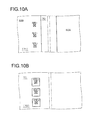
- FIG. 10A and FIG. 10B are schematic, partial plan views of the memory cell unit array according to Example 1 as viewed along an arrow mark 10 A and an arrow mark 10 B of FIG. 6 .
- FIG. 11A and FIG. 11B are schematic, partial plan views of the memory cell unit array according to Example 1 as viewed along an arrow mark 11 A and an arrow mark 11 B of FIG. 6 .
- FIG. 12A and FIG. 12B are schematic, partial cross-sectional views of the memory cell unit array according to Example 1 as it is cut along a virtual perpendicular plane parallel to a second direction.
- FIG. 13A and FIG. 13B are schematic, partial plan views of the memory cell unit array according to Example 1 as viewed along an arrow mark 13 A and an arrow mark 13 B of FIG. 12A and FIG. 12B .
- FIG. 14A and FIG. 14B are schematic, partial plan views of the memory cell unit array according to Example 1 as viewed along an arrow mark 14 A and an arrow mark 14 B of FIG. 12A and FIG. 12B .
- FIG. 15 is a schematic, partial plan view of the memory cell unit array according to Example 1 as viewed along an arrow mark 15 of FIG. 12A and FIG. 12B .
- FIG. 16 is a schematic, partial cross-sectional view of a modified example of the memory cell unit array according to Example 1 as it is cut along the virtual perpendicular plane parallel to the first direction.
- FIG. 17A and FIG. 17B are schematic, partial plan views of the modified example of the memory cell unit array according to Example 1 as it is viewed an arrow mark 17 A and an arrow mark 17 B of FIG. 16 .
- FIG. 18A and FIG. 18B are schematic, partial plan views of the modified example of the memory cell unit array according to Example 1 as viewed along an arrow mark 18 A and an arrow mark 18 B of FIG. 16 .
- FIG. 19 is a perspective view schematically showing nonvolatile memory cells in Example 2.
- FIG. 20 is a conceptual, partial cross-sectional view for describing components of a memory cell unit array according to Example 2.
- FIG. 21A and FIG. 21B are schematic, partial plan views of the memory cell unit array according to Example 2 as viewed along an arrow mark 21 A and an arrow mark 21 B of FIG. 20 .
- FIG. 22A and FIG. 22B are schematic, partial plan views of the memory cell unit array according to Example 2 as viewed along an arrow mark 22 A and an arrow mark 22 B of FIG. 20 .
- FIG. 23A and FIG. 23B are schematic, partial plan views of the memory cell unit array according to Example 2 as viewed along an arrow mark 23 A and an arrow mark 23 B of FIG. 20 .
- FIG. 24A and FIG. 24B are schematic, partial plan views of the memory cell unit array according to Example 2 as viewed along an arrow mark 24 A and an arrow mark 24 B of FIG. 20 .
- FIG. 25A and FIG. 25B are schematic, partial plan views of the memory cell unit array according to Example 2 as viewed along an arrow mark 25 A and an arrow mark 25 B of FIG. 20 .
- FIG. 26 is a schematic, partial plan view of the memory cell unit array according to Example 2 as viewed along an arrow mark 26 of FIG. 20 .
- FIG. 27 is a conceptual, partial cross-sectional view for describing components of the memory cell unit array according to Example 2.
- FIG. 28A and FIG. 28B are schematic, partial plan views of the memory cell unit array according to Example 2 as viewed along an arrow mark 28 A and an arrow mark 28 B of FIG. 27 .
- FIG. 29A and FIG. 29B are schematic, partial plan views of the memory cell unit array according to Example 2 as viewed along an arrow mark 29 A and an arrow mark 29 B of FIG. 27 .
- FIG. 30A and FIG. 30B are schematic, partial plan views of the memory cell unit array according to Example 2 as viewed along an arrow mark 30 A and an arrow mark 30 B of FIG. 27 .
- FIG. 31A and FIG. 31B are schematic, partial plan views of the memory cell unit array according to Example 2 as viewed along an arrow mark 31 A and an arrow mark 31 B of FIG. 27 .
- FIG. 32A and FIG. 3B are schematic, partial plan views of the memory cell unit array according to Example 2 as viewed along an arrow mark 32 A and an arrow mark 32 B of FIG. 27 .
- FIG. 33 is a perspective view schematically showing nonvolatile memory cells in Example 3.
- FIG. 34 is a conceptual, partial cross-sectional view for describing components of a memory cell unit array according to Example 3.
- FIG. 35 is a schematic, partial plan view of the memory cell unit array according to Example 3 as viewed along an arrow mark 35 of FIG. 34 .
- FIG. 36 is a schematic, partial plan views of the memory cell unit array according to Example 3 as viewed along an arrow mark 36 of FIG. 34 .
- FIG. 37 is a schematic, partial plan view of the memory cell unit array according to Example 3 as viewed along an arrow mark 37 of FIG. 34 .
- FIG. 38 is a schematic, partial plan views of the memory cell unit array according to Example 3 as viewed along an arrow mark 38 of FIG. 34 .
- FIG. 39 is a schematic, partial plan view of the memory cell unit array according to Example 3 as viewed along an arrow mark 39 of FIG. 34 .
- FIG. 40 is a schematic, partial plan view of the memory cell unit array according to Example 3 as viewed along an arrow mark 40 of FIG. 34 .
- FIG. 41 is a schematic, partial plan view of the memory cell unit array according to Example 3 as viewed along an arrow mark 41 of FIG. 34 .
- FIG. 42 is a schematic, partial plan view of the memory cell unit array according to Example 3 as viewed along an arrow mark 42 of FIG. 34 .
- FIG. 43 is a schematic, partial plan view of the memory cell unit array according to Example 3 as viewed along an arrow mark 43 of FIG. 34 .
- FIG. 44 is a perspective view schematically showing nonvolatile memory cells in Example 4.
- FIG. 45 is a diagram describing modified examples of an arrangement of memory cell units of Example 5.
- FIG. 46 is a diagram describing modified examples of the arrangement of the memory cell units of Example 5.
- FIG. 47 is a diagram describing a modified example of the arrangement of the memory cell units of Example 5.
- FIG. 48 is a diagram describing a modified example of the arrangement of the memory cell units of Example 5.
- FIG. 49 is a view schematically showing of an arrangement of a bit line, a word line, a contact hole in a conventional cross-point memory cell unit.
- FIG. 50A and FIG. 50B are views schematically showing an arrangement of control circuits, contact holes, and the like in a cross-point memory cell unit as disclosed in Japanese Patent Application Laid-open No. 2009-223971.
- FIG. 51A is a view schematically showing an arrangement of first wires (bit lines) in the cross-point memory cell unit as disclosed in Japanese Patent Application Laid-open No. 2009-223971 shown in FIG. 50A and FIG. 50B
- FIG. 51B and FIG. 51C are schematic, partial cross-sectional views taken along an arrow mark B-B and an arrow mark C-C of FIG. 50A .
- Example 1 Memory Cell Unit Array According to Present Disclosure
- Example 5 Modified Example of Arrangement of Control Circuit
- first wires connected to a first control circuit that constitutes a memory cell unit and first wires connected to a first control circuit that constitutes an adjacent memory cell unit are alternately disposed.
- control circuit is covered with an inter-layer insulating layer
- the first control circuit and the first wires are connected to one another via a first contact hole formed in the inter-layer insulating layer, and
- a second control circuit and second wires are connected to one another via a second contact hole formed in the inter-layer insulating layer.
- control circuit is covered with an inter-layer insulating layer
- the first control circuit and the first wires are connected to one another via a first control wire and a first contact hole formed in the inter-layer insulating layer,
- the second control circuit and the second wires are connected to one another via a second control wire and a second contact hole formed in the inter-layer insulating layer,
- the first control circuit and the second control wire do not overlap each other in upper and lower directions
- the second control circuit and the first control wire do not overlap each other in the upper and lower directions.
- positions of projection images of the first contact holes are positioned at equal intervals along the second direction.
- the second wires are, at end portions thereof, connected to the second control circuit.
- One ends of odd-numbered second wires as viewed in a plane are connected to one of second control circuits (to be described later), and one ends of even-numbered second wires as viewed in the plane are connected to the other of the second control circuits (to be described later).
- First wires belonging to one of the memory cell units are common to the first wires belonging to a memory cell unit adjacent to this memory cell unit along the first direction.
- the first wires are connected to a first control circuit at appropriately center portions of the first wires.
- the memory cell unit array including the various favorable embodiments described above, it is possible to employ an embodiment in which the memory cell units are arranged in-line along the second direction and arranged offset from each other along the first direction. In this case, it is possible to employ a configuration in which the memory cell units are arranged in-line along the second direction and arranged offset from each other along the first direction by 1 ⁇ 2 of a length of the memory cell unit along the second direction.
- the memory cell unit array including the various favorable embodiments described above, it is possible to employ a configuration in which the memory cell units are arranged in a stretcher bond pattern of brick patterns. In this case, it is possible to employ a configuration in which half of the first wires that constitute the memory cell unit are connected to the first control circuit that constitutes the memory cell unit, and the other half of the first wires that constitute the memory cell unit are connected to the first control circuit that constitutes an adjacent memory cell unit adjacent thereto in the first direction.
- the first control circuit is constituted of two circuits, a first(I) control circuit and a first(II) control circuit,
- the second control circuit is constituted of two circuits, a second(I) control circuit and a second(II) control circuit,
- the first(I) control circuit is disposed along a first side, which extends in parallel to the second direction,
- the first(II) control circuit extends in parallel to the second direction and is disposed along a third side of the control circuit, which is opposed to the first side,
- the second(I) control circuit is disposed along a second side of the control circuit, which extends in parallel to the first direction, and
- the second(II) control circuit extends in parallel to the first direction and is disposed along a fourth of the control circuit, which is opposed to the second side.
- the second(II) control circuit extends in parallel to the first direction and is disposed along a fourth of the control circuit, which is opposed to the second side.
- the second(I) control circuit is disposed to occupy the entire second side and occupy a part of the first side and a part of the third side,
- the second(II) control circuit is disposed to occupy the entire fourth side and occupy a part of the first side and a part of the third side,
- the first(I) control circuit is disposed to occupy a part of the first side
- the first(II) control circuit is disposed to occupy a part of the third side.
- the second control circuit is constituted of two circuits, a second(I) control circuit and a second(II) control circuit,
- the second(I) control circuit is disposed along a second side of the control circuit, which extends in parallel to the first direction,
- the second(II) control circuit extends in parallel to the first direction and is disposed along a fourth side of the control circuit, which is opposed to the second side, and
- the first control circuit is disposed to extend from the first side of the control circuit, which extends in parallel to the second direction, to the third side of the control circuit, which is opposed to the first side.
- the first control circuit is constituted of two circuits, a first(I) control circuit and a first(II) control circuit,
- the second control circuit is disposed to extend from a second side of the control circuit, which extends in parallel to the first direction, to a fourth side of the control circuit, which is opposed to the second side,
- the first(I) control circuit is disposed along a first side of the control circuit, which extends in parallel to the second direction, and
- the first(II) control circuit extends in parallel to the first direction and is disposed along a third side of the control circuit, which is opposed to the first side.
- the nonvolatile memory cell is multi-layered having N layers (where N ⁇ 2).
- N where N ⁇ 2
- the first wires are formed in first wire layers that are N layers
- the second wires are formed in second wire layers that are N layers
- the nonvolatile memory cell is formed between the first wire layer and the second wire layer.
- the first wires are formed in first wire layers that are (N/2+1) layers (where N is an even number equal to two or more), the second wires are formed in a second wire layer that is (N/2) layer, and
- the nonvolatile memory cell is formed between the first wire layer and the second wire layer.
- the first wires are formed in a first wire layer that is (N/2) layer (where N is an even number equal to two or more), the second wires are formed in second wire layers that are (N/2+1) layers, and
- the nonvolatile memory cell is formed between the first wire layer and the second wire layer.
- the first wires are formed in first wire layers that are ⁇ (N+1)/2 ⁇ layers (where N is an odd number equal to three or more), the second wires are formed in second wire layers that are ⁇ (N+1)/2 ⁇ layers, and
- the nonvolatile memory cell is formed between the first wire layer and the second wire layer.
- the nonvolatile memory cell includes a nonvolatile memory device.
- the nonvolatile memory device can include
- phase-change nonvolatile memory device Phase Change RAM, PCRAM
- (C) a spin-transfer torque magnetoresistance effect device that writes and erases information using magnetization reversal of a storage layer due to spin torque, i.e., application of magnetization reversal due to spin transfer torque
- These configurations and structures of the nonvolatile memory devices can be well-known configurations and structures.
- the phase-change nonvolatile memory device has a structure in which a memory unit that functions as a resistance-change layer is disposed between two electrodes.
- a resistance-change layer information is stored using changes in electrical resistance value (hereinafter, sometimes simply referred to as “resistance value”).
- the phase-change (resistance-change) nonvolatile memory device can have, for example,
- a resistance-change layer formed of a material having a Colossal Magneto-Resistance effect (CMR effect).
- CMR effect Colossal Magneto-Resistance effect
- a phase-change memory device PRAM
- PMC Programmable metallization Cell
- ReRAM Resistance Random Access Memory
- the resistance-change layer when the resistance-change layer is constituted of an ion conductor including metal, specifically, the resistance-change layer can be constituted of an electrically conductive or semi-electrically conductive, thin film (e.g., thin film formed of GeSbTe, GeTe, GeSe, GeS, SiGeTe, SiGeSbTe) containing at least one kind of element (atom) selected from a group of copper (Cu), silver (Ag), and zinc (Zn) and at least one kind of element (chalcogen) (atom) selected from a group of tellurium (Te), sulfur (S), and selenium (Se).
- an electrically conductive or semi-electrically conductive, thin film e.g., thin film formed of GeSbTe, GeTe, GeSe, GeS, SiGeTe, SiGeSbTe
- a laminate structure of such a thin film and a thin film formed of, for example, Ag, an Ag alloy, Cu, a Cu alloy, Zn, or a Zn alloy can be employed or it is also possible to employ a configuration in which a film (rare earth oxide thin film) formed of an oxide of at least one kind of rare earth elements selected from a group of La, Ce, Pr, Nd, Sm, Eu, Gd, Tb, Dy, Ho, Er, Yb and Y of rare earth elements or an oxide film such as Hf, Ta, and W is formed in the whole of that thin film or a part of that thin film in a film-thickness direction.
- a film (rare earth oxide thin film) formed of an oxide of at least one kind of rare earth elements selected from a group of La, Ce, Pr, Nd, Sm, Eu, Gd, Tb, Dy, Ho, Er, Yb and Y of rare earth elements or an oxide film such as Hf, Ta, and W is formed in the whole of that thin film or
- the resistance-change layer can be constituted of an electrically conductive or semi-electrically conductive, thin film (e.g., amorphous thin film formed of GeSbTeGd) containing at least one kind of element (atom) selected from a group of germanium (Ge), silicon (Si), antimony (Sb), and indium (In) and at least one kind of element (chalcogen) (atom) selected from a group of tellurium (Te), sulfur (S), and selenium (Se).
- an electrically conductive or semi-electrically conductive, thin film e.g., amorphous thin film formed of GeSbTeGd
- the resistance-change layer is formed of a laminate structure of a high-resistance layer and an ion source layer, specifically, it can have a configuration in which the ion source layer includes at least one kind of a metal element as an element that can be positively ionized and further includes at least one kind of element (chalcogen) (atom) selected from a group of tellurium (Te), sulfur (S), and selenium (Se) as an element negatively ionized.
- a metal element and chalcogen are coupled to form a metal chalcogenide layer (chalcogenide-based material layer).
- the metal chalcogenide layer mainly has an amorphous structure and functions as an ion supply source.
- the ion source layer is formed having a resistance value lower than the high-resistance layer in an initial state or erasing state.
- the metal element that constitutes the metal chalcogenide layer is favorably a chemically stable element that can be present in a metal state in the ion source layer containing chalcogen described above such that it is deoxidized on an electrode during writing operation and forms a conduction path (filament) in the metal state.
- Examples of such a metal element can include copper (Cu), aluminum (Al), germanium (Ge), and zinc (Zn), and, for example, transition metals of the 4A, 5A, and 6A Groups in the periodic table of the elements, i.e., Ti (titanium), Zr (zirconium), Hf (hafnium), V (vanadium), Nb (niobium), Ta (tantalum), Cr (chromium), Mo (molybdenum), and W (tungsten).
- Ti titanium
- Zr zirconium
- Hf hafnium
- V vanadium
- Nb niobium
- Ta tantalum
- Cr chromium
- Mo mobdenum
- W tungsten
- Al (aluminum), Cu (copper), Ge (germanium), Si (silicon), or the like may be an additive element added to the ion source layer.
- a constituent material of the ion source layer can include ZrTeAl, TiTeAl, CrTeAl, WTeAl, TaTeAl, and CuTe. Further, such examples can also include CuZrTeAl obtained by adding Cu to ZrTeAl, CuZrTeAlGe obtained by further adding Ge to it, and CuZrTeAlSiGe obtained by further adding Si to it as an additive element. Alternatively, such examples can also include ZrTeMg obtained by replacing Al by Mg.
- a similar additive element can be used.
- a constituent material of the ion source layer can also include TaTeAlGe.
- sulfur (S), selenium (Se), or iodine (I) may be used other than tellurium (Te).
- Specific examples of a constituent material of the ion source layer can include ZrSAl, ZrSeAl, and ZrIAl.
- the metal element that constitutes the metal chalcogenide layer is constituted of a metal element (M) that easily reacts with tellurium (Te) contained in the high-resistance layer and a laminate structure, that is, a Te/ion source layer (including the metal element M) is used, a stabilized structure, that is, M-Te/ion source layer can be obtained due to heat treatment after film deposition.
- the metal element (M) that easily reacts with tellurium (Te) can include aluminum (Al) and magnesium (Mg).
- silicon (Si) is an additive element also capable of improving a retaining characteristic, and hence favorably added to the ion source layer together with zirconium (Zr), for example. It should be noted that the effect of preventing the film from being pealed off cannot be expected if added silicon (Si) is too little, and a favorable memory operation characteristic cannot be obtained if it is too much. Silicon (Si) content of the ion source layer is favorably within a range of approximately 10 to 45 atomic %.
- the high-resistance layer When a predetermined voltage is applied on the nonvolatile memory device, at least one kind of metal element is diffused in the high-resistance layer as an element that can be positively ionized, and a resistance value of the high-resistance layer is lowered.
- the high-resistance layer has a function as a barrier in electric conduction.
- the high-resistance layer has a resistance value higher than that of the ion source layer when a predetermined voltage is applied between the electrode and the electrically conductive material layer (or wires) in an initialized state or erasing state.
- the high-resistance layer includes a layer formed of a compound having tellurium (Te) as a main component, which behaves as a negative ion component, for example, as described above.
- a compound having tellurium (Te) can include AlTe, MgTe, and ZnTe.
- content of aluminum (Al) in AlTe is favorably 20 atomic % or more, 60 atomic % or less, for example.
- the high-resistance layer may contain an oxide such as an aluminum oxide (AlO x ).
- an initial resistance value of the high-resistance layer is favorably 1 M ⁇ or more and a resistance value of the low-resistance state is favorably several hundreds k ⁇ or less. That is to say, the nonvolatile memory device stores information or the like by changing the resistance value of this high-resistance layer. In order to read out a resistance state of a miniaturized nonvolatile memory device at high speed, it is favorable to lower the resistance value in a low-resistance state as much as possible. However, a resistance value is 40 k ⁇ to 100 k ⁇ when information (data) or the like is written under a condition of 20 ⁇ A to 50 ⁇ A, 2V.
- the initial resistance value of the nonvolatile memory device is higher than this value.
- the above-mentioned resistance value is considered as being appropriate.
- the high-resistance layer can have not only a mono-layer configuration but also a multi-layer configuration, in this case, a lower layer containing tellurium as a main, negative ion component is held in contact with an electrode on a high-resistance layer side and an upper layer contains an element that is a negative ion component other than tellurium.
- examples of the high-resistance layer can also include SiN, SiO 2 , Gd 2 O 3 , and a material containing fluorine (e.g., MgF 2 , AlF 3 , CaF 2 , LiF).
- a material containing fluorine e.g., MgF 2 , AlF 3 , CaF 2 , LiF.
- the high-resistance layer contains tellurium (Te) as a main, negative ion component
- Te tellurium
- a metal element diffused in the high-resistance layer is stabilized when the resistance of the high-resistance layer is lowered, it becomes easy to retain the low-resistance state.
- tellurium (Te) has coupling force with the metal element, which is smaller than that of an oxide or silicon compound, and the metal element diffused in the high-resistance layer easily moves to the ion source layer. Therefore, an erasing characteristic is improved. That is to say, the retaining characteristic of writing data in the low-resistance state is improved and it becomes possible to lower the voltage when data is erased.
- variations in the resistance value in the erasing state can be reduced with respect to multiple writing/erasing operations.
- electronegativity for chalcogenide compound, an absolute value generally increases in the order of tellurium ⁇ selenium ⁇ sulfur ⁇ oxygen. Therefore, as less oxygen is present in the high-resistance layer and chalcogenide having a lower electronegativity is used, the effect of improvement is higher.
- Examples of a constituent material of the electrode can include W (tungsten), WN (tungsten nitride), Cu (copper), Al (aluminum), Mo (molybdenum), Au (gold), Pt (platinum), Ti (titanium), TiN (titanium nitride), TiW (titanium-tungsten), Mo (molybdenum), Ta (tantalum), and silicide.
- the electrode is constituted of a material such as copper (Cu), in which ion conduction may occur due to an electrical field, the surface of the electrode may be covered with a material such as tungsten (W), a tungsten nitride (WN), a titanium nitride (TiN), and a tantalum nitride (TaN), in which ion conduction and thermophoresis hardly occur.
- a material such as tungsten (W), a tungsten nitride (WN), a titanium nitride (TiN), and a tantalum nitride (TaN), in which ion conduction and thermophoresis hardly occur.
- examples of a constituent material of the electrode can include a material more hardly ionized in comparison with Al (aluminum), for example, a metal film containing at least one kind of Cr (chromium), W (tungsten), Co (cobalt), Si (silicon), Au (gold), Pd (palladium), Mo (molybdenum), Ir (iridium), and Ti (titanium), and an oxide film or nitride film thereof.
- a well-known electrically conductive material including an electrically conductive material similar to the electrode can be used for the electrically conductive material layer (or wires).
- it may include a laminate structure of a base layer formed of Cr, Ti, or the like and a Cu layer, an Au layer, a Pt layer, or the like, which is formed thereon.
- it can also be constituted of a mono-layer of Ta or the like or a laminate structure of Cu, Ti, and the like.
- the electrode and the electrically conductive material layer (or wires) can be formed by a PVD method or CVD method including sputtering, for example.
- a voltage pulse in a “positive direction” (e.g., the high-resistance layer is set to have a negative potential while the ion source layer is set to have a positive potential) is applied on the nonvolatile memory device in an initial state (high-resistance state).
- the metal element contained in the ion source layer is ionized, diffused in the high-resistance layer, coupled with electrons and precipitated on the electrode, or remains in the high-resistance layer and forms an impurity state.
- a conduction path including the metal element is formed in the information storage layer, more specifically, the high-resistance layer, the resistance of the information storage layer is lowered (information-storing state).
- the information storage layer is retained in the low-resistance state. In this manner, the information is written and retained.
- a write once storage apparatus i.e., a so-called PROM (Programmable Read Only Memory)
- PROM Programmable Read Only Memory
- storing (recording) of information is completed only by this information storing process.
- a rewriting process is required for the use of a storage apparatus capable of rewriting information multiple times, i.e., a RAM (Random Access Memory) or EEPROM, for example.
- a voltage pulse in a “negative direction” (e.g., the high-resistance layer is set to have a positive potential while the ion source layer is set to have a negative potential) is applied on the nonvolatile memory device in the low-resistance state.
- the metal element precipitated on the electrode is ionized and dissolved in the ion source layer.
- the conduction path including the metal element disappears, and a state in which the resistance of the high-resistance layer is high (initial state or erasing state) is obtained. After that, even when the application of voltage on the nonvolatile memory device is cancelled, the information storage layer is retained in the high-resistance state.
- the written information is erased.
- voltage in, for example, a “positive direction” e.g., the high-resistance layer is set to have a negative potential while the ion source layer is set to have a positive potential
- that value is lower than the value of voltage applied when information is stored (written).
- the high-resistance state is set corresponding to information of “0” and the low-resistance state is set corresponding to information of “1”, “0” is changed to in the information-writing process and “1” is changed to “0” in the information-erasing process.
- the operation of providing the low-resistance state and the operation of providing the high-resistance state are respectively set corresponding to the writing operation and the erasing operation, the erasing operation and the writing operation may be set corresponding to opposite resistance states.
- the resistance-change layer is constituted of a chalcogenide-based material
- examples of the chalcogenide-based material can include a compound of metal and Se or Te, such as GeSbTe, ZnSe, and GaSnTe.
- the resistance-change layer is constituted of a material having a Colossal Electro-Resistance effect (CER effect)
- examples of such a material can include a 3-element-based perovskite type transition metal oxide (PrCaMnO 3 or SrTiO 3 ) and a 2-element-based transition metal oxide (CiO, NiO, CuO, TiO 2 , Fe 3 O 4 ).
- the resistance-change layer is constituted of a chalcogenide-based material. Pulsed, large current (e.g., 200 microamperes, 20 nanoseconds) is allowed to flow through the resistance-change layer in short time. After that, rapid cooling is performed, and the phase-change material that constitutes the resistance-change layer is brought into an amorphous state and exhibits high-resistance.
- Pulsed, large current e.g. 200 microamperes, 20 nanoseconds
- pulsed, small current e.g., 100 microamperes, 100 nanoseconds
- slow cooling is performed, and the phase-change material that constitutes the resistance-change layer is brought into a crystalline state and exhibits low-resistance.
- the ReRAM is formed of a multi-element-based metal oxide constituted of a plurality of metal elements and oxygen such as a perovskite-type metal oxide or formed of a 2-element-based metal oxide constituted of one kind of metal element and oxygen.
- the ReRAM can be of a unipolar (non-polar) type or bipolar type or can also be of a filament type (fuse-antifuse type) or an interface type.
- the nonvolatile memory device can be constituted of a nonvolatile, magnetic memory device having a so-called magnetoresistance effect.
- a nonvolatile memory device can include a tunnel magnetoresistance effect device (MRAM) using a current/magnetic field-inverting method.
- MRAM tunnel magnetoresistance effect device
- spin-RAM spin-transfer torque magnetoresistance effect device
- the latter includes an in-plane magnetization method and a perpendicular magnetization method.
- a storage layer for storing information also called recording layer, magnetization reversal layer, or magnetization free layer
- a middle layer also called magnetization reference layer, magnetization fixed layer, or magnetization fixation layer
- TMR Tunnelnel Magnetoresistance
- GMR Giant Magnetoresistance
- spin polarization current When a writing current (hereinafter, sometimes referred to as “spin polarization current”) is allowed to flow from the storage layer to the fixation layer in an anti-parallel magnetization state, the magnetization of the storage layer is inverted due to spin torque that acts when electrons are implanted into the storage layer from the fixation layer, and the direction of magnetization of the storage layer, the direction of magnetization of the fixation layer, and the direction of magnetization of the storage layer become parallel.
- the spin polarization current is allowed to flow from the fixation layer to the storage layer in a parallel magnetization state
- the magnetization of the storage layer is inverted due to spin torque that acts when electrons are implanted into the fixation layer from the storage layer, and the direction of magnetization of the storage layer and the direction of magnetization of the fixation layer become anti-parallel.
- a structure double spin filter structure in which a plurality of fixation layers, a middle layer, a storage layer, a middle layer, and a plurality of fixation layers constitute a laminate structure having a TMR effect or GMR effect.
- the fixation layers, the middle layer, and the storage layer constitute a laminate structure having a TMR effect” refer to a structure in which a middle layer formed of a non-magnetic film that functions as a tunnel insulating film is sandwiched between the fixation layer formed of a magnetic material and the storage layer formed of a magnetic material.
- a middle layer serves to interrupt magnetic coupling between the storage layer and the fixation layer and allow a tunnel current to flow.
- Examples of a constituent material of the storage layer can include a ferromagnetic material such as nickel (Ni), iron (Fe), and cobalt (Co), an alloy (e.g., Co—Fe, Co—Fe—B, Co—Fe—Ni, Fe—Pt, Ni—Fe) of such a ferromagnetic material, an alloy obtained by adding gadolinium (Gd) to the alloy thereof, an alloy (e.g., Co—Fe—B) obtained by mixing a non-magnetic element (e.g., tantalum, boron, chromium, platinum, silicon, carbon, nitrogen) in the alloy thereof, an oxide (e.g., ferrite: Fe—MnO) including one or more kinds of Co, Fe, and Ni, a group of intermetallic compounds (Heusler alloy: NiMnSb, Co 2 MnGe, Co 2 MnSi, Co 2 CrAl, etc.) called half-metallic ferromagnetic material, and an oxide (
- the perpendicular magnetization type for further increasing the perpendicular magnetic anisotropy, heavy rare-earth elements such as terbium (Tb), dysprosium (Dy), and holmium (Ho) may be added to such an alloy or an alloy containing them may be laminated.
- the storage layer and the fixation layer can essentially have any crystallinity. It may be polycrystalline, monocrystalline, or amorphous. Further, the storage layer can also have a mono-layer configuration, a lamination configuration in which a plurality of different ferromagnetic material layers described above are laminated, or a lamination configuration in which a ferromagnetic material layer and a non-magnetic material layer are laminated.
- the fixation layer can include the above-mentioned constituent material (ferromagnetic material) of the storage layer.
- the fixation layer can be formed of a laminate of a Co layer and a Pt layer, a laminate of a Co layer and a Pd layer, a laminate of a Co layer and a Ni layer, a laminate of a Co layer and a Tb layer, a Co—Pt alloy layer, a Co—Pd alloy layer, a Co—Ni alloy layer, a Co—Fe alloy layer, a Co—Tb alloy layer, a Co layer, a Fe layer, or a Co—Fe—B alloy layer.
- the fixation layer can be formed of a Co—Fe—B alloy layer.
- the direction of magnetization of the fixation layer is a reference of information. Therefore, the direction of magnetization has not be changed by storing (recording) or reading information. However, it does not necessarily need to be fixed in a particular direction.
- the fixation layer can also have a structure formed of a plurality of fixation layers. Such a structure is called lamination ferrimagnetic structure.
- the lamination ferrimagnetic structure is a laminate structure having antiferromagnetic coupling, i.e., a structure in which inter-layer exchange coupling between two magnetic material layers becomes antiferromagnetic. It is also called synthetic antiferromagnetic coupling (SAF: Synthetic Antiferromagnet). It refers to a structure in which inter-layer exchange coupling between the two magnetic material layers becomes antiferromagnetic or ferromagnetic in a manner that depends on a non-magnetic layer and has been reported in, for example, pp 2304-2307 of Physical Review Letters by S. S. Parkin et.
- Examples of a constituent material of the non-magnetic layer can include ruthenium (Ru) and an alloy thereof and can also include Os, Re, Ir, Au, Ag, Cu, Al, Bi, Si, B, C, Cr, Ta, Pd, Pt, Zr, Hf, W, Mo, and Nb, and alloys thereof.
- ruthenium ruthenium
- Os, Re, Ir, Au, Ag, Cu, Al, Bi, Si, B, C, Cr, Ta, Pd, Pt, Zr, Hf, W, Mo, and Nb and alloys thereof.
- the fixation layer can have a magnetostatic coupling structure, and an antiferromagnetic layer may be disposed adjacent to the fixation layer.
- the magnetostatic coupling structure is a structure by which antiferromagnetic coupling can be obtained due to a magnetic field leaked from end surfaces of two magnetic material layers.
- examples of a constituent material of the antiferromagnetic layer can include an iron-manganese alloy, a nickel-manganese alloy, a platinum-manganese alloy, a platinum-chromium-manganese alloy, an iridium-manganese alloy, a rhodium-manganese alloy, a cobalt oxide, a nickel oxide, and an iron oxide (Fe 2 O 3 ).
- the middle layer is favorably formed of a non-magnetic film. That is to say, in the spin-transfer torque magnetoresistance effect device, the middle layer, which constitutes the laminate structure having the TMR effect, is favorably constituted of a non-magnetic film formed of an insulating material.
- examples of a constituent material of the non-magnetic film formed of the insulating material can include various insulating materials, dielectric materials, and semiconductor materials such as a magnesium oxide (MgO), a magnesium nitride, a magnesium fluoride, an aluminum oxide (AlO x ), an aluminum nitride (AlN), a silicon oxide (SiO x ), a silicon nitride (SiN), TiO 2 , Cr 2 O 3 , Ge, NiO, CdO x , HfO 2 , Ta 2 O 5 , Bi 2 O 3 , CaF, SrTiO 3 , AlLaO 3 , Al—N—O, BN, and ZnS.
- MgO magnesium oxide
- AlO x aluminum oxide
- AlN aluminum nitride
- SiO x silicon oxide
- SiN silicon nitride
- examples of a constituent material of the non-magnetic film that constitutes the laminate structure having the GMR effect can include electrically conductive materials such as Cu, Ru, Cr, Au, Ag, Pt, Ta, and an alloy thereof. If the electrical conductivity is high (the resistivity is several hundreds ⁇ cm or less), an arbitrary non-metal material may be employed. It is desirable to appropriately select a material in which interfacial reaction with the storage layer and the fixation layer hardly occurs.
- the middle layer formed of the insulating material can be obtained by oxidation or nitriding of a metal film formed by sputtering, for example. More specifically, when an aluminum oxide (AlO x ) or magnesium oxide (MgO) is used as an insulating material that constitutes the middle layer, there can be, for example, a method of oxidizing aluminum or magnesium formed by sputtering in the atmosphere, a method of oxidizing aluminum or magnesium formed by sputtering in plasma, a method of oxidizing aluminum or magnesium formed by sputtering in IPC plasma, a method of naturally oxidizing aluminum or magnesium formed by sputtering in oxygen, a method of oxidizing aluminum or magnesium formed by sputtering with oxygen radicals, a method of emitting a ultraviolet ray when aluminum or magnesium formed by sputtering is subjected to natural oxidation in oxygen, a method of depositing a film of aluminum or magnesium by reactive sputtering, and a method of depositing a
- the above-mentioned various layers can be formed by a physical vapor deposition method (PVD method), for example, sputtering, an ion beam deposition method, or a vacuum vapor deposition method or by a chemical vapor deposition method (CVD method) represented by an ALD (Atomic Layer Deposition) method.
- PVD method physical vapor deposition method
- CVD method chemical vapor deposition method
- patterning of the above-mentioned layers can be performed by a reactive ion etching method (RIE method) or an ion milling method (ion beam etching method). It is favorable to continuously form various layers in a vacuum apparatus. It is favorable to perform patterning thereafter.
- RIE method reactive ion etching method
- ion milling method ion milling method
- the fixation layer As an electrically connection state between the fixation layer and the first wires (or the second wires), there can be, for example, an embodiment in which the first wires (or the second wires) are directly connected to the fixation layer or an embodiment in which the first wires (or the second wires) are connected to the fixation layer via the antiferromagnetic layer.
- the direction of magnetization in the storage layer is defined. In this manner, information is written in the storage layer.
- a base layer formed of Ta, Cr, Ru, Ti, or the like may be formed between the first wires (or the second wires) and the antiferromagnetic layer.
- cap layer between the storage layer and the wires in order to prevent mutual diffusion of atoms that constitutes the wires and the connection portion and atoms that constitutes the storage layer, to lower contact resistance, and to prevent oxidation of the storage layer.
- the cap layer can include a laminate structure of a Ta layer, an Ru layer, a Pt layer, a Ti layer, a W layer, an MgO layer, and an Ru film/Ta film.
- a stereoscopic shape of the laminate structure be columnar (cylindrical), from the perspective of easiness of machining and for the purpose of ensuring directional uniformity of an axis of easy magnetization in the storage layer.
- a triangular cylinder, a quadrangular prism, a hexagonal prism, or an octagonal prism (including those having rounded lateral sides or lateral edges), or an elliptic cylinder can also be employed.
- a base layer formed of Ta, Cr, Ru, Ti, or the like may be formed between the laminate structure and the wires in order to enhance the crystallinity of a magnetic layer of the laminate structure, which is brought into contact with the wires.
- a redox-active substance layer is constituted of at least one kind of a group of nickel (Ni), cobalt (Co), chromium (Cr), titanium (Ti), tantalum (Ta), iron (Fe), aluminum (Al), vanadium (V), a reductant (H x WO 3 ) of a tungsten oxide (WO 3 ), and an oxide of vanadium (V).
- the inter-electrode material layer includes an amorphous thin film as a base material, the amorphous thin film containing at least one kind of chalcogenide-based materials such as sulfur (S), selenium (Se), and tellurium (Te) and at least one kind of germanium (Ge), silicon (Si), antimony (Sb), and indium (In).
- chalcogenide-based materials such as sulfur (S), selenium (Se), and tellurium (Te) and at least one kind of germanium (Ge), silicon (Si), antimony (Sb), and indium (In).
- the first wires and the second wires may be formed of a mono-layer structure of copper (Cu), aluminum (Al), gold (Au), platinum (Pt), titanium (Ti), molybdenum (Mo), tantalum (Ta), tungsten (W), TiN, TiW, WN, silicide, or the like.
- the first wires and the second wires may have a laminate structure of a base layer formed of Cr, Ti, or the like and a Cu layer, an Au layer, a Pt layer, or the like formed thereon.
- it can also be constituted of a mono-layer of Ta or the like or a laminate structure of Cu, Ti, and the like.
- Those wires can be formed by the PVD method including sputtering, for example.
- the first wires, the second wires are formed on the inter-layer insulating layer.
- a constituent material of the inter-layer insulating layer can include a silicon oxide (SiO 2 ), a silicon nitride (SiN), SiON, SOG, NSG, BPSG, PSG, BSG, and LTO.
- the inter-layer insulating layer can be formed by the CVD method or the PVD method including sputtering, for example.
- Examples of a constituent material of the contact hole can include polysilicon doped with impurities, tungsten, metal having a high-melting point such Ti, Pt, Pd, Cu, TiW, TiNW, WSi 2 , and MoSi 2 , and metal silicide.
- the contact hole be formed by the CVD method or the PVD method including sputtering, for example.
- the nonvolatile memory cell is formed between the first wires and the second wires.
- a selection device for controlling current flowing the nonvolatile memory cell is provided between the first wires and the nonvolatile memory cell or between the second wires and the nonvolatile memory cell.
- the selection device can include a device having a non-linear current-voltage characteristic, such as a bidirectional diode and a varistor.
- Examples of the control circuit can include a well-known circuit formed on a silicon semiconductor substrate.
- the control circuit includes, for example, various decoders and a sense amplifier.
- Example 1 relates to a memory cell unit array according to the present disclosure.
- FIG. 1 and FIG. 2 show schematic plan views of a part of a memory cell unit array according to Example 1. Note that FIG. 1 shows some of first wires and FIG. 2 shows some of second wires. Further, a perspective view of FIG. 3A schematically shows nonvolatile memory cells. FIG. 3B and FIG. 3C show equivalent circuit diagrams of the nonvolatile memory cells. In addition, FIG. 4 shows a perspective view conceptually showing the nonvolatile memory cells. FIG. 5 shows a plan view schematically showing a part of the memory cell unit array, which is a plan view showing some of the first wires. In addition, FIG. 6 , FIG. 7 , FIG. 8 , and FIG.
- FIG. 9 show schematic, partial cross-sectional views of the memory cell unit array as it is cut along the virtual perpendicular plane parallel to the first direction.
- FIG. 10A , FIG. 10B , FIG. 11A , and FIG. 11B show schematic, partial plan views thereof as viewed along an arrow mark 10 , an arrow mark 10 B, an arrow mark 11 A, and an arrow mark 11 B of FIG. 6A .
- FIG. 12A and FIG. 12B show schematic, partial cross-sectional views of the memory cell unit array as it is cut along another virtual perpendicular plane parallel to the second direction.
- FIG. 15 show schematic, partial plan views of the memory cell unit array as viewed along an arrow mark 13 A, an arrow mark 13 B, an arrow mark 14 A, an arrow mark 14 B, and an arrow mark 15 of each of FIG. 12A and FIG. 12B .
- boundaries of the memory cell unit are indicated by long dashed short dashed lines and these schematic, partial plan views are schematic, partial plan views of a portion of a region “A” of FIG. 8 .
- memory cell units 10 are arranged in a two-dimensional matrix form in the first direction and the second direction, the memory cell units 10 being each constituted of
- nonvolatile memory cells 20 that are disposed in a region in which the first wires 31 and the second wires 41 overlap one another and connected to the first wires 31 and the second wires 41 .
- Each of the memory cell units 10 includes, below the memory cell unit 10 , a control circuit that controls an operation of the memory cell unit 10 .
- the control circuit is constituted of a first control circuit that controls an operation of the nonvolatile memory cell 20 that constitutes the memory cell unit 10 via the first wires 31 , and a second control circuit that controls an operation of the nonvolatile memory cell 20 that constitutes the memory cell unit 10 via the second wires 41 .
- the second wires 41 that constitute the memory cell unit 10 are connected to the second control circuit that constitutes this memory cell unit 10 .
- the control circuit is disposed below the memory cell unit 10 .
- a projection image of the control circuit may be positioned in a projection image of the memory cell unit 10 , the projection image of the control circuit and the projection image of the memory cell unit 10 may overlap each other, or a part of the projection image of the control circuit may be positioned in the projection image of the memory cell unit 10 (i.e., the control circuit and the memory cell unit 10 may be slightly offset from each other in the upper and lower directions).
- first wires 31 that constitute the memory cell unit 10 are connected to the first control circuit that constitutes this memory cell unit 10 and others of the first wires 31 that constitute the memory cell unit 10 are connected to the first control circuit that constitutes an adjacent memory cell unit 10 adjacent thereto in the first direction.
- first wires 31 connected to the first control circuit that constitutes this memory cell unit 10 and the first wires 31 connected to the first control circuit that constitutes the adjacent memory cell unit 10 are alternately disposed.
- first wires 31 B shown by the dotted lines
- first wires 31 A shown by the thin, solid lines
- control circuit is covered with inter-layer insulating layers 71 , 72 , 73 , 74 .
- the first control circuit and first wires 31 A, 31 B are connected to one another via first contact holes 32 A, 32 B formed in the inter-layer insulating layers (in some cases, subscripts will be omitted).
- the second control circuit and the second wires 41 are connected to one another via second contact holes formed in the inter-layer insulating layers 42 A, 42 B (in some cases, subscripts will be omitted).
- positions of projection images of the first contact holes are positioned at equal intervals along the second direction (e.g., see first contact holes 32 A and first contact holes 32 B shown by white circle symbols “A” and white square symbols “B” of FIG. 5 ). Note that, although the contact holes are positioned outside of the control circuit in FIG. 1 , FIG. 2 , FIG. 5 , and FIG. 16 , they are actually provided within the control circuit.
- the second wires 41 are, at end portions thereof, connected to the second control circuit. Note that one ends of odd-numbered second wires 41 as viewed in a plane are connected to a second(I) control circuit 60 A (to be described later) and one ends of even-numbered second wires 41 as viewed in the plane are connected to a second(II) control circuit 60 B (to be described later).
- the memory cell units 10 are arranged in-line along the second direction and arranged offset from each other along the first direction. Specifically, the memory cell units 10 are arranged in-line along the second direction and arranged offset from each other along the first direction by 1 ⁇ 2 of a length of the memory cell unit 10 along the second direction. Alternatively, the memory cell units 10 are arranged in a stretcher bond pattern of brick patterns.
- Example 1 half of the first wires 31 that constitute the memory cell unit 10 are connected to the first control circuit that constitutes this memory cell unit 10 .
- the other half of the first wires 31 that constitute the memory cell unit 10 are connected to the first control circuit that constitutes the adjacent memory cell unit 10 adjacent thereto in the first direction.
- the first control circuit is constituted of two circuits, the first(I) control circuit 50 A and the first(II) control circuit 50 B.
- the second control circuit is constituted of two circuits, the second(I) control circuit 60 A and the second(II) control circuit 60 B.
- the first(I) control circuit 50 A is disposed along a first side 10 a of the control circuit, which extends in parallel to the second direction.
- the first(II) control circuit 50 B extends in parallel to the second direction and is disposed along a third side 10 c of the control circuit, which is opposed to the first side 10 a.
- the second(I) control circuit 60 A is disposed along a second side 10 b of the control circuit, which extends in parallel to the first direction.
- the second(II) control circuit 60 B extends in parallel to the first direction and is disposed along a fourth side 10 d of the control circuit, which is opposed to the second side 10 b .
- a fourth side 10 d of the control circuit which is opposed to the second side 10 b .
- the second(I) control circuit 60 A is disposed to occupy the entire second side 10 b and occupy a part of the first side 10 a and a part of the third side 10 c.
- the second(II) control circuit 60 B is disposed to occupy the entire fourth side 10 d and occupy a part of the first side 10 a and a part of the third side 10 c.
- the first(I) control circuit 50 A is disposed to occupy a part of the first side 10 a.
- the first(II) control circuit 50 B is disposed to occupy a part of the third side 10 c . Note that, in Example 1, a region occupied by the first(I) control circuit 50 A and a region occupied by the first(II) control circuit 50 B are arranged in point symmetry with respect to a center of the control circuit. A region occupied by the second(I) control circuit 60 A and a region occupied by the second(II) control circuit 60 B are arranged in point symmetry with respect to the center of the control circuit.
- a region occupied by the first(I) control circuit 50 A and a region occupied by the first(II) control circuit 50 B are arranged in line symmetry with respect to an axis parallel to the second direction, the axis passing through the center of the control circuit.
- the first wires 31 are formed in a first wire layer that is (N/2) layer (one layer, first wire layer 30 ).
- the second wires 41 are formed in second wire layers that are (N/2+1) layers (two layers, second wire layers 40 1 , 40 2 ).
- the nonvolatile memory cells 20 are formed between the first wire layer and the second wire layers. That is to say, one of the nonvolatile memory cell 20 is formed between the first wires 31 and the second wires 41 1 . Further, the other of the nonvolatile memory cell 20 is formed between the first wires 31 and the second wires 41 2 .
- the first wire 41 1 and the second wires 41 2 are independently and separately driven. Writing, reading, and erasing of information are independently performed in the two nonvolatile memory cells 20 provided sandwiching two first wires 31 .
- the nonvolatile memory cell 20 according to Example 1 is formed of a phase-change nonvolatile memory device, specifically, a resistance-change nonvolatile memory device. More specifically, a resistance-change layer is formed of a laminate structure of a high-resistance layer and an ion source layer. Further, in Example 1, the nonvolatile memory cell 20 is constituted of nonvolatile memory devices 21 and selection devices 22 each having a non-linear current-voltage characteristic, such as bidirectional diodes. The selection devices 22 are provided between the first wires 31 and the nonvolatile memory devices 21 or between the second wires 41 and the nonvolatile memory devices 21 . The selection devices 22 control current flowing through the nonvolatile memory devices 21 .
- the high-resistance layer is formed of an aluminum oxide (AlO x ) and the ion source layer is formed of a copper-tellurium (Cu—Te) alloy film.
- the first wires 31 and the second wires 41 are formed of copper (Cu)
- the contact holes are formed of tungsten (W)
- the inter-layer insulating layer is formed of SiO 2 .
- the control circuit having well-known configuration and structure is formed in a silicon semiconductor substrate 70 on the basis of a well-known method.
- a power supply line and various signal lines are provided in a portion of the silicon semiconductor substrate 70 between the memory cell unit and the memory cell unit and a drive circuit that drives the memory cell unit is provided as a peripheral circuit in a periphery of the memory cell unit array, illustrations thereof are omitted.
- FIG. 6 , FIG. 7 , FIG. 8 , and FIG. 9 are schematic, partial cross-sectional views of the memory cell unit according to Example 1 as it is cut along the virtual perpendicular plane parallel to the first direction
- FIG. 12A and FIG. 12B are schematic, partial cross-sectional views of the memory cell unit array according to Example 1 as it is cut along another virtual perpendicular plane parallel to the second direction
- FIG. 10A , FIG. 10B , FIG. 11A , FIG. 11B , FIG. 13A , FIG. 13B , FIG. 14A , FIG. 14B , and FIG. 15 that are schematic, partial plan views thereof.
- FIG. 10A , FIG. 10B , FIG. 11A , FIG. 11B , FIG. 13A , FIG. 13B , FIG. 14A , FIG. 14B , and FIG. 15 are schematic, partial plan views thereof.
- FIG. 6 is a schematic, partial cross-sectional view of the memory cell unit as it is cut along a perpendicular virtual plane including a first wire 31 B indicated as “ ⁇ ” of FIG. 5 .
- FIG. 7 is a schematic, partial cross-sectional view of the memory cell unit as it is cut along a perpendicular virtual plane including a first wire 31 A indicated as “ ⁇ ” of FIG. 5 .
- FIG. 8 is a schematic, partial cross-sectional view of the memory cell unit as it is cut along a perpendicular virtual plane including a first wire 31 B indicated as “ ⁇ ” of FIG. 5 .
- FIG. 9 is a schematic, partial cross-sectional view of the memory cell unit as it is cut along a perpendicular virtual plane including a first wire 31 A indicated as “ ⁇ ” of FIG. 5 .
- first contact holes 32 B 1 extend upwardly from the first(II) control circuit 50 B through the inter-layer insulating layer 71 .
- second contact holes 42 A 11 , 42 A 12 extend upwardly from the second(I) control circuit 60 A through the inter-layer insulating layer 71 .
- first contact holes 32 B 2 extend upwardly from the first contact holes 32 B 1 through the inter-layer insulating layer 72 .
- second contact holes 42 A 21 , 42 22 extend upwardly from second contact holes 42 A 11 , 42 12 through the inter-layer insulating layer 72 .
- FIG. 10A first contact holes 32 B 1 extend upwardly from the first(II) control circuit 50 B through the inter-layer insulating layer 71 .
- second contact holes 42 A 11 , 42 A 12 extend upwardly from the second(I) control circuit 60 A through the inter-layer insulating layer 71 .
- first contact holes 32 B 2 extend upwardly from the first contact holes 32 B 1 through the inter-layer insulating layer 72 .
- first contact holes 32 B 3 extend upwardly from the first contact holes 32 B 2 through the inter-layer insulating layer 73 .
- the second wires 41 1 extend in the second direction from the second contact holes 42 A 22 on the inter-layer insulating layer 72 and second contact holes 42 A 31 extend upwardly from the second contact holes 42 A 21 through the inter-layer insulating layer 73 .
- the first wires 31 extend in the first direction from the first contact holes 32 B 3 on the inter-layer insulating layer 73 .
- second contact holes 42 A 41 extend upwardly from the second contact holes 42 A 31 through the inter-layer insulating layer 74 .
- the second wires 41 1 extend in the second direction from the second contact holes 42 A 41 on the inter-layer insulating layer 74 .
- one first wire 31 is connected to the first(II) control circuit 50 B via one set of the first contact holes 32 B 1 , 32 B 2 , 32 B 3 upwardly extending from the first(II) control circuit 50 B. It should be noted that it is not limited to such a configuration.
- FIG. 16 shows a schematic, partial cross-sectional view of a modified example of the memory cell unit array according to Example 1 as it is cut along the virtual perpendicular plane parallel to the first direction.
- FIG. 17A , FIG. 17B , FIG. 18A , and FIG. 18B show schematic, partial plan views of the modified example of the memory cell unit array according to Example 1 as viewed along an arrow mark 17 , an arrow mark 17 B, an arrow mark 18 A, and an arrow mark 18 B of FIG. 16A .
- FIG. 16 is a schematic, partial cross-sectional view similar to FIG. 6 , and further, those schematic, partial plan views are schematic, partial plan views of a portion of a region “A” of FIG. 16 .
- the first contact holes 32131 extend upwardly from the first(II) control circuit 50 B through the inter-layer insulating layer 71 as shown in FIG. 17A and first control wires 33 extend from the first contact holes 32 B 1 on the inter-layer insulating layer 71 toward the adjacent memory cell unit, as shown in FIG. 17B .
- the first contact holes 32 B 2 extend upwardly from the first control wires 33 through the inter-layer insulating layer 72 .
- the first contact holes 32 B 3 extend upwardly from the first contact holes 32 B 2 through the inter-layer insulating layer 73 .
- first wires 31 B extend in the first direction from the first contact holes 32 B 3 on the inter-layer insulating layer 73 . Note that the first wires 31 B are separated from one another but electrically connected to one another through the first control wires 33 .
- the plurality of nonvolatile memory cells and the control circuit overlap one another in upper and lower directions. Therefore, a highest-density arrangement of nonvolatile memory cells can be provided.
- a memory cell unit array in which cross-point memory cell units are arranged in a two-dimensional matrix form, which has configuration and structure with high area efficiency, can be provided. Thus, manufacturing yield can be improved.
- wires (control wires) are not basically provided directly on the control circuit. Therefore, without problems of occurrence of parasitic capacitance caused by wires, noise occurrence in wires, and interference between wires and the control circuit, a memory cell unit array having a high reliability can be provided.
- Example 2 is a modification of Example 1.
- FIG. 19 shows a perspective view schematically showing nonvolatile memory cells in Example 2.
- FIG. 20 and FIG. 27 show conceptual, partial cross-sectional views for describing components of a memory cell unit array according to Example 2.
- FIG. 32B show schematic, partial plan views of the memory cell unit array according to Example 2 as it is viewed along an arrow mark 21 , an arrow mark 21 B, an arrow mark 22 A, an arrow mark 22 B, an arrow mark 23 A, an arrow mark 23 B, an arrow mark 24 A, an arrow mark 24 B, an arrow mark 25 A, an arrow mark 25 B, and an arrow mark 26 of FIG. 20A and an arrow mark 28 , an arrow mark 28 B, an arrow mark 29 A, an arrow mark 29 B, an arrow mark 30 A, an arrow mark 30 B, an arrow mark 31 A, an arrow mark 31 B, an arrow mark 32 A, and an arrow mark 32 B of FIG. 27A .
- a nonvolatile memory cell 20 is formed between the first wire layer and the second wire layer.
- the second wires 41 1 , 41 2 , 41 3 , 41 4 are independently and separately driven.
- the first wires 31 1 , 31 2 , 31 3 , 31 4 are similarly driven at the same time, they may be independently and separately driven.
- connection of the first wires 31 1 , 31 2 , 31 3 , 31 4 to first control circuits 50 A, 50 B is as follows.
- control circuits are covered with inter-layer insulating layers 71 , 72 , 73 , 74 and the first control circuits 50 A, 50 B and the first wires 31 are connected to one another via the first control wires 33 and first contact holes 32 A, 32 B formed in the inter-layer insulating layers.
- Second control circuits 60 A, 60 B and the second wires 41 are connected to one another via second control wires 43 and second contact holes 42 A, 42 B formed in inter-layer insulating layers.
- the first control circuits 50 A, 50 B and the second control wires 43 do not overlap each other in the upper and lower directions and the second control circuits 60 A, 60 B and the first control wires 33 do not overlap each other in the upper and lower directions.
- first contact holes 32 A, 32 B in one of the memory cell units 10 and first contact holes 32 A, 32 B in a memory cell unit 10 adjacent to this memory cell unit 10 in the first direction are projected in the virtual perpendicular plane parallel to the second direction, positions of projection images of the first contact holes 32 A, 32 B are positioned at equal intervals along the second direction.
- first contact holes 32 B 1 extend upwardly from the first(II) control circuit 50 B through the inter-layer insulating layer 71 .
- the first control wires 33 extend from the first contact holes 32 B 1 on the inter-layer insulating layer 71 toward the adjacent memory cell unit.
- the first contact holes 32 B 2 extend upwardly from the first control wires 33 through the inter-layer insulating layer 72 .
- the first contact holes 32 B 3 extend upwardly from the first contact holes 32 B 2 through the inter-layer insulating layer 73 . As shown in FIG.
- the first contact holes 32 B 4 extend upwardly from the first contact holes 32 B 3 through the inter-layer insulating layer 74 .
- the first wires 31 1 extend in the first direction from the first contact holes 32 B 4 on the inter-layer insulating layer 74 .
- first contact holes 32 B 5 extend upwardly from the first wires 31 1 through an inter-layer insulating layer 75 .
- first contact holes 32 B 6 extend upwardly from the first contact holes 32 B 5 through an inter-layer insulating layer 76 .
- the first wires 31 2 extend in the first direction from the first contact holes 32 B 6 on the inter-layer insulating layer 76 .
- first contact holes 32 B 7 extend upwardly from the first wires 31 2 through an inter-layer insulating layer 77 .
- first contact holes 32 B 8 extend upwardly from the first contact holes 32 B 7 through an inter-layer insulating layer 78 .
- the first wires 31 3 extend in the first direction from the first contact holes 32 B 8 on the inter-layer insulating layer 78 .
- first contact holes 32 B 9 extend upwardly from the first wires 31 3 through an inter-layer insulating layer 79 .
- first contact holes 32 B 10 extend upwardly from the first contact holes 32 B 9 through an inter-layer insulating layer 80 .
- the first wires 31 4 extend in the first direction from the first contact holes 32 B 10 on the inter-layer insulating layer 80 . Note that, although the first wires 31 1 , 31 2 , 31 3 , 31 4 are separated from one another, they are electrically connected to one another through the first control wires 33 .
- connection of the second control circuits 60 A, 60 B of the second wires 41 1 , 41 2 , 41 3 , 41 4 is as follows. That is to say, as shown in FIG. 28A , the second contact holes 42 A 11 , 42 A 12 extend upwardly from the second(I) control circuit 60 B through the inter-layer insulating layer 71 . Further, second contact holes 42 A 13 , 42 A 14 (not shown) upwardly extend. As shown in FIG. 28B , first control wires 43 3 extend from second contact holes 42 A 13 (not shown) on the inter-layer insulating layer 71 up to regions in which second contact holes 42 A 23 should be formed. As shown in FIG.
- the second contact holes 42 A 21 , 42 A 22 , 42 A 23 , second contact holes 42 A 24 (not shown) upwardly extend through the inter-layer insulating layer 72 .
- first control wires 43 4 extend from the second contact holes 42 A 24 (not shown) on the inter-layer insulating layer 72 up to regions in which second contact holes 42 A 34 should be formed.
- the first control wires 43 3 , 43 4 are connected to the second(I) control circuit 60 B.
- second contact holes 42 A 31 , 42 A 32 , 42 A 33 , 42 A 34 upwardly extend through the inter-layer insulating layer 73 .
- the second wires 41 1 extend in the second direction from the second contact holes 42 A 34 on the inter-layer insulating layer 73 .
- second contact holes 42 A 41 , 42 A 42 , 42 A 43 upwardly extend through the inter-layer insulating layer 74 .
- second contact holes 42 A 51 , 42 A 52 , 42 A 53 extend upwardly from the second contact holes 42 A 41 , 42 A 42 , 42 A 43 through the inter-layer insulating layer 75 .
- the second wires 41 2 extend in the second direction from the second contact holes 42 A 53 on the inter-layer insulating layer 75 .
- second contact holes 42 A 61 , 42 A 62 upwardly extend through the inter-layer insulating layer 76 .
- second contact holes 42 A 71 , 42 A 72 extend upwardly from the second contact holes 42 A 61 , 42 A 62 through the inter-layer insulating layer 77 .
- the second wires 41 3 extend in the second direction from the second contact holes 42 A 72 on the inter-layer insulating layer 77 .
- second contact holes 42 A 81 upwardly extend through the inter-layer insulating layer 78 .
- second contact holes 42 A 91 extend upwardly from the second contact holes 42 A 81 through the inter-layer insulating layer 79 .
- the second wires 41 4 extend in the second direction from the second contact holes 42 A 91 on the inter-layer insulating layer 79 .
- Example 2 configuration and structure of the memory cell unit array according to Example 2 can be similar to the configuration and structure of the memory cell unit array described in Example 1, and hence detailed descriptions thereof will be omitted.
- Example 3 is also a modification of Example 1.
- FIG. 33 shows a perspective view schematically showing nonvolatile memory cells in Example 3.
- FIG. 34 shows a conceptual, partial cross-sectional view for describing components of a memory cell unit array according to Example 3.
- FIG. 35 , FIG. 36 , FIG. 37 , FIG. 38 , FIG. 39 , FIG. 40 , FIG. 41 , FIG. 42 , and FIG. 43 show schematic, partial plan views of the memory cell unit array according to Example 3 as it is viewed along an arrow mark 35 , an arrow mark 36 , an arrow mark 37 , an arrow mark 38 , an arrow mark 39 , an arrow mark 40 , an arrow mark 41 , an arrow mark 42 , and an arrow mark 43 of FIG. 34 .
- first wires 31 are formed in first wire layers that are (N/2+1) layers (where N is an even number equal to two or more).
- Second wires 41 are formed in a second wire layer that is (N/2) layer and a nonvolatile memory cell 20 is formed between each of the first wire layers and the second wire layer.
- first wires 31 1 , 31 2 , 31 3 , 31 4 , 31 5 are formed in first wire layers that are five layers and second wires 41 1 , 41 2 , 41 3 , 41 4 are formed in second wire layers that are four layers.
- the nonvolatile memory cell 20 is formed between the first wire layer and the second wire layer.
- the second wires 41 1 , 41 2 , 41 3 , 41 4 are independently and separately driven.
- the first wires 31 1 , 31 3 , 31 5 are similarly driven at the same time.
- the first wires 31 2 , 31 4 are similarly driven at the same time.
- the first wires 31 1 , 31 3 , 31 5 and the first wires 31 2 , 31 4 are separately driven. Note that the first wires 31 1 , 31 2 , 31 3 , 31 4 , 31 5 may be separately driven.
- the first contact holes 32 B extend upwardly from, for example, the first(II) control circuit 50 B through an inter-layer insulating layer and the first control wires extend toward an adjacent memory cell unit on the inter-layer insulating layer.
- first contact holes 32 B 11 , 32 B 12 , 32 B 13 , 32 B 14 extend upwardly from the first control wires (not shown) through an inter-layer insulating layer 72 .
- first wires 31 1-1 , 31 1-3 extend in the first direction from the first contact holes 32 B 11 , 32 B 13 on the inter-layer insulating layer 72 .
- first contact holes 32 B 21 , 32 B 22 , 32 B 23 , 32 B 24 extend upwardly from the first contact holes 32 B 11 , 32 B 12 , 32 B 13 , 32 B 14 through an inter-layer insulating layer 73 .
- first contact holes 32 B 31 , 32 B 32 , 32 B 33 , 32 B 34 extend upwardly from the first contact holes 32 B 21 , 32 B 22 , 32 B 23 , 32 B 24 through an inter-layer insulating layer 74 .
- first wires 31 2-1 , 31 2-3 extend in the first direction from the first contact holes 32 B 32 , 32 B 34 on the inter-layer insulating layer 74 .
- first contact holes 32 B 31 , 32 B 32 , 32 B 33 , 32 B 34 extend upwardly from the first contact holes 32 B 21 , 32 B 22 , 32 B 23 , 32 B 24 through an inter-layer insulating layer 75 .
- first contact holes 32 B 41 , 32 B 42 , 32 B 43 , 32 B 44 extend upwardly from the first contact holes 32 B 31 , 32 B 32 , 32 B 33 , 32 B 34 through an inter-layer insulating layer 76 .
- first wires 31 3 - 1 , 31 3 - 3 extend in the first direction from first contact holes 32 B 41 , 32 B 43 on the inter-layer insulating layer 76 .
- first contact holes 32 B 51 , 32 B 52 , 32 B 53 , 32 B 54 extend upwardly from the first contact holes 32 B 41 , 32 B 42 , 32 B 43 , 32 B 44 through an inter-layer insulating layer 77 .
- first contact holes 32 B 61 , 32 B 62 , 32 B 63 , 32 B 64 extend upwardly from the first contact holes 32 B 51 , 32 B 52 , 32 B 53 , 32 B 54 through an inter-layer insulating layer 78 .
- first wires 31 4-1 , 31 4-3 extend in the first direction from first contact holes 32 B 62 , 32 B 64 on the inter-layer insulating layer 78 .
- first contact holes 32 B 71 , 32 B 73 extend upwardly from first contact holes 32 B 61 , 32 B 63 through the inter-layer insulating layer 79 .
- first contact holes 32 B 81 , 32 B 83 extend upwardly from the first contact holes 32 B 71 , 32 B 73 through an inter-layer insulating layer 80 .
- first wires 31 5-1 , 31 5-3 extend in the first direction from the first contact holes 32 B 81 , 32 B 83 on the inter-layer insulating layer 80 .
- Example 3 configuration and structure of the memory cell unit array according to Example 3 can be similar to the configuration and structure of the memory cell unit array described in Example 1, and hence detailed descriptions thereof will be omitted.
- Example 4 is also a modification of Example 1.
- a perspective view of FIG. 44 schematically shows nonvolatile memory cells in Example 4.
- first wires 31 are formed in first wire layers that are ⁇ (N+1)/2 ⁇ layers (where N is an odd number equal to three or more)
- second wires 41 are formed in second wire layers that are ⁇ (N+1)/2 ⁇ layers
- a nonvolatile memory cell is formed between the first wire layer and the second wire layer.
- the first wires 31 are formed in first wire layers that are four layers and the second wires 41 are formed second wire layers that are four layers.
- a total of seven nonvolatile memory cells 20 are formed between the first wire layers and the second wire layers in the upper and lower directions.
- the second wires are independently and separately driven. Further, odd-numbered first wires in the upper and lower directions are similarly driven at the same time while even-numbered first wires in the upper and lower directions are similarly driven at the same time. That is to say, the odd-numbered first wires in the upper and lower directions and the even-numbered first wires in the upper and lower directions are separately driven. All the odd- and even-numbered first wires in the upper and lower directions may be separately driven.
- Connection of the first wires 31 to first control circuits 50 A, 50 B and connection of the second wires 41 to second control circuits 60 A, 60 B can be similar to those described in Example 2 or Example 3. Except for the above-mentioned points, configuration and structure of a memory cell unit array according to Example 4 can be similar to the configuration and structure of the memory cell unit array described in Example 1, and hence detailed descriptions thereof will be omitted.
- Example 5 is a modification of Example 1 to Example 4.
- Example 5 is a modification relating to planar shape and arrangement of the first control circuit and the second control circuit.
- FIG. 45 and FIG. 46 two memory cell units arranged in the first direction are shown in each of examples of memory cell units. Further, in FIG. 47 and FIG. 48 , a number of memory cell units arranged in the first direction and the second direction are shown.
- a second control circuit is constituted of two circuits, a second(I) control circuit 60 A and a second(II) control circuit 60 B.
- the second(I) control circuit 60 A is disposed along a second side 10 b of the control circuit, which extends in parallel to the first direction.
- the second(II) control circuit 60 B extends in parallel to the first direction and is disposed along a fourth side 10 d of the control circuit, which is opposed to the second side 10 b.
- a first control circuit 50 is disposed to extend from a first side 10 a of the control circuit, which extends in parallel to the second direction, to a third side 10 c of the control circuit, which is opposed to the first side 10 a.
- a first control circuit is constituted of two circuits, a first(I) control circuit 50 A and a first( ) control circuit 50 B.
- a second control circuit 60 is disposed to extend from a second side 10 b of the control circuit, which extends in parallel to the first direction, to a fourth side 10 d of the control circuit, which is opposed to the second side 10 b.
- the first( ) control circuit 50 A is disposed along the first side 10 a of the control circuit, which extends in parallel to the second direction.
- the first(II) control circuit 50 B extends in parallel to the first direction and is disposed along a third side 10 c of the control circuit, which is opposed to the first side 10 a.
- a length of a first control circuit along the second direction in a certain memory cell unit and a length of a first control circuit along the second direction in a memory cell unit adjacent to this memory cell unit are different from each other.
- each of the first(I) control circuit and the first(II) control circuit is divided into two parts. Division regions 51 and a region 52 between the memory cell unit and the memory cell unit are continuous with each other in the first direction. Such an arrangement makes it easy to dispose a power supply line and various signal lines, for example.
- FIG. 45 a length of a first control circuit along the second direction in a certain memory cell unit and a length of a first control circuit along the second direction in a memory cell unit adjacent to this memory cell unit are different from each other.
- each of the first(I) control circuit and the first(II) control circuit is divided into two parts. Division regions 51 and a region 52 between the memory cell unit and the memory cell unit are continuous with each other in the first direction. Such an arrangement makes it easy to dispose a power supply line and various signal
- a region occupied by the first(I) control circuit 50 A and a region occupied by the first(II) control circuit 50 B are arranged in point symmetry with respect to a center of the control circuit
- a region occupied by the second(I) control circuit 60 A and a region occupied by the second(II) control circuit 60 B are arranged in point symmetry with respect to the center of the control circuit.
- the region occupied by the first(I) control circuit 50 A and the region occupied by the first(II) control circuit 50 B are arranged in line symmetry with respect to an axis parallel to the second direction, the axis passing through the center of the control circuit.
- the region occupied by the second(I) control circuit 60 A and the region occupied by the second(II) control circuit 60 B are arranged in line symmetry with respect to an axis parallel to the first direction, the axis passing through the center of the control circuit.
- a region occupied by a first(I) control circuit 50 A and a region occupied by a first(II) control circuit 50 B are arranged in line symmetry with respect to an axis parallel to the second direction, the axis passing through a center of a control circuit.
- a region occupied by a second(I) control circuit 60 A and a region occupied by a second(II) control circuit 60 B are arranged in line symmetry with respect to an axis parallel to the first direction, the axis passing through the center of the control circuit.
- a region occupied by a first(I) control circuit 50 A and a region occupied by a first(II) control circuit 50 B are arranged in point symmetry with respect to a center of a control circuit and a region occupied by a second(I) control circuit 60 A and a region occupied by a second(II) control circuit 60 B are arranged in point symmetry with respect to the center of the control circuit.
- first(I) control circuits 50 A and first(II) control circuits 50 B are different among memory cell units A, memory cell units B, memory cell units C, and memory cell units D.
- the memory cell unit array according to the present disclosure has been described above on the basis of the favorable Examples. However, the memory cell unit array according to the present disclosure is not limited to those Examples.
- the arrangements of the first control circuits and the second control circuits, the configurations and structures of the memory cell unit arrays, which have been described in those Examples, are examples.
- the configurations and structures of the nonvolatile memory cells are also examples. They can be appropriately changed.
- the planar shapes of the first control circuits and the second control circuits, the planar shapes and wirings of the first wires and the second wires, the first control wires, and the second control wires, and the like are examples. They can be appropriately changed.
- a memory cell unit array including
- memory cell units arranged in a two-dimensional matrix form in a first direction and a second direction, the memory cell units being each constituted of
- each of the memory cell units includes, below the memory cell unit, a control circuit that controls an operation of the memory cell unit,
- control circuit is constituted of
- the second wires that constitute the memory cell unit are connected to the second control circuit that constitutes the memory cell unit,
- first wires that constitute the memory cell unit are connected to a first control circuit that constitutes an adjacent memory cell unit adjacent thereto in the first direction.
- the first wires connected to the first control circuit that constitutes the memory cell unit and the first wires connected to the first control circuit that constitutes the adjacent memory cell unit are alternately disposed.
- control circuit is covered with an inter-layer insulating layer
- the first control circuit and the first wires are connected to one another via a first contact hole formed in the inter-layer insulating layer, and
- the second control circuit and the second wires are connected to one another via a second contact hole formed in the inter-layer insulating layer.
- control circuit is covered with an inter-layer insulating layer
- the first control circuit and the first wires are connected to one another via a first control wire and a first contact hole formed in the inter-layer insulating layer,
- the second control circuit and the second wires are connected to one another via a second control wire and a second contact hole formed in the inter-layer insulating layer,
- the first control circuit and the second control wire do not overlap each other in the upper and lower directions
- the second control circuit and the first control wire do not overlap each other in the upper and lower directions.
- positions of projection images of the first contact holes are positioned at equal intervals along the second direction.
- the second wires are, at end portions thereof, connected to the second control circuit.
- the memory cell units are arranged in-line along the second direction and arranged offset from each other along the first direction.
- the memory cell units are arranged in-line along the second direction and arranged offset from each other along the first direction by 1 ⁇ 2 of a length of the memory cell unit along the second direction.
- the other half of the first wires that constitute the memory cell unit are connected to the first control circuit that constitutes the adjacent memory cell unit adjacent thereto in the first direction.
- the memory cell units are arranged in a stretcher bond pattern of brick patterns.
- the other half of the first wires that constitute the memory cell unit are connected to the first control circuit that constitutes the adjacent memory cell unit adjacent thereto in the first direction.
- the first control circuit is constituted of two circuits, a first(I) control circuit and a first(II) control circuit,
- the second control circuit is constituted of two circuits, a second(I) control circuit and a second(II) control circuit,
- the first(I) control circuit is disposed along a first side of the control circuit, which extends in parallel to the second direction,
- the first(II) control circuit extends in parallel to the second direction and is disposed along a third side of the control circuit, which is opposed to the first side,
- the second(I) control circuit is disposed along a second side of the control circuit, which extends in parallel to the first direction, and
- the second(II) control circuit extends in parallel to the first direction and is disposed along a fourth side of the control circuit, which is opposed to the second side.
- the second(I) control circuit is disposed to occupy the entire second side and occupy a part of the first side and a part of the third side,
- the second(II) control circuit is disposed to occupy the entire fourth side and occupy a part of the first side and a part of the third side,
- the first(I) control circuit is disposed to occupy a part of the first side
- the first(II) control circuit is disposed to occupy a part of the third side.
- the second control circuit is constituted of two circuits, a second(I) control circuit and a second(II) control circuit,
- the second(I) control circuit is disposed along a second side of the control circuit, which extends in parallel to the first direction,
- the second(II) control circuit extends in parallel to the first direction and is disposed along a fourth side of the control circuit, which is opposed to the second side, and
- the first control circuit is disposed to extend from the first side of the control circuit, which extends in parallel to the second direction, to the third side of the control circuit, which is opposed to the first side.
- the first control circuit is constituted of two circuits, a first(I) control circuit and a first(II) control circuit,
- the second control circuit is disposed to extend from a second side of the control circuit, which extends in parallel to the first direction, to a fourth side of the control circuit, which is opposed to the second side,
- the first(I) control circuit is disposed along a first side of the control circuit, which extends in parallel to the second direction, and
- the first(II) control circuit extends in parallel to the first direction and is disposed along a third side of the control circuit, which is opposed to the first side.
- a region occupied by the first(I) control circuit and a region occupied by the first(II) control circuit are arranged in point symmetry with respect to a center of the control circuit.
- [A17] The memory cell unit array according to any one of [A12], [A13], [A15], and [A16], in which
- a region occupied by the first(I) control circuit and a region occupied by the first(II) control circuit are arranged in line symmetry with respect to an axis parallel to the second direction, the axis passing through a center of the control circuit.
- a region occupied by the second(I) control circuit and a region occupied by the second(II) control circuit are arranged in point symmetry with respect to a center of the control circuit.
- a region occupied by the second(I) control circuit and a region occupied by the second(II) control circuit are arranged in line symmetry with respect to an axis parallel to the first direction, the axis passing through a center of the control circuit.
- a ratio of (a length of the first control circuit along the second direction)/(an entire length of the control circuit along the second direction) is 1 ⁇ 3 to 2 ⁇ 3.
- a ratio of (a length of the first control circuit along the second direction)/(an entire length of the control circuit along the second direction) is 1 ⁇ 2.
- a length of a first control circuit along the second direction in one of the memory cell units is L 1
- a length of a first control circuit along the second direction in an adjacent memory cell unit adjacent to the one memory cell unit is L 1 ′
- an entire length of the control circuit along the second direction is L 0
- L 0 L 1 +L 1 ′ is satisfied.
- the nonvolatile memory cell is multi-layered having N layers (where N ⁇ 2).
- the first wires are formed in first wire layers that are N layers,
- the second wires are formed in second wire layers that are N layers, and
- the nonvolatile memory cell is formed between the first wire layer and the second wire layer.
- the first wires are formed in first wire layers that are (N/2+1) layers (where N is an even number equal to two or more),
- the second wires are formed in a second wire layer that is (N/2) layer, and
- the nonvolatile memory cell is formed between the first wire layer and the second wire layer.
- the first wires are formed in a first wire layer that is (N/2) layer (where N is an even number equal to two or more),
- the second wires are formed in second wire layers that are (N/2+1) layers, and
- the nonvolatile memory cell is formed between the first wire layer and the second wire layer.
- the first wires are formed in first wire layers that are ⁇ (N+1)/2 ⁇ layers (where N is an odd number equal to three or more),
- the second wires are formed in second wire layers that are ⁇ (N+1)/2 ⁇ layers, and
- the nonvolatile memory cell is formed between the first wire layer and the second wire layer.
- the nonvolatile memory cell includes a nonvolatile memory device and a selection device, and
- the nonvolatile memory device includes a phase-change nonvolatile memory device.
- 10 . . . memory cell unit 10 a . . . first side of control circuit, 10 b . . . second side of control circuit, 10 c . . . third side of control circuit, 10 d . . . fourth side of control circuit, 20 . . . nonvolatile memory cell, 21 . . . nonvolatile memory device, 22 . . . selection device, 30 . . . first wire layer, 31 , 31 A, 32 B . . . first wire, 32 A, 32 B . . . first contact hole, 33 . . . first control wire, 40 . . . second wire layer, 41 . . . second wire, 42 A, 42 B .
Landscapes
- Engineering & Computer Science (AREA)
- Microelectronics & Electronic Packaging (AREA)
- Semiconductor Memories (AREA)
- Physics & Mathematics (AREA)
- Geometry (AREA)
- Condensed Matter Physics & Semiconductors (AREA)
- General Physics & Mathematics (AREA)
- Computer Hardware Design (AREA)
- Power Engineering (AREA)
- Mram Or Spin Memory Techniques (AREA)
Abstract
Description
-
- a plurality of first wires extending in the first direction,
- a plurality of second wires that are disposed separately from the first wires in upper and lower directions and extend in the second direction unlike the first wires, and
- a nonvolatile memory cell that is disposed in a region in which the first wires and the second wires overlap one another and connected to the first wires and the second wires, in which
-
- a first control circuit that controls an operation of the nonvolatile memory cell that constitutes the memory cell unit via the first wires, and
- a second control circuit that controls an operation of the nonvolatile memory cell that constitutes the memory cell unit via the second wires,
-
- is favorably satisfied. However, in some cases, L0>L1+L1′ may be possible.
(F) a carbon nanotube memory device (memory device that is constituted of a carbon nanotube itself or includes wires and electrodes in various nonvolatile memory cells (various nonvolatile memory devices), which are constituted of carbon nanotubes), and
(G) an organic thin-film memory device (using an organic material for an organic compound layer that stores information). These configurations and structures of the nonvolatile memory devices can be well-known configurations and structures.
(g) an ReRAM (Resistance Random Access Memory) in which a metal oxide is sandwiched by two electrodes and a pulse voltage is applied on the electrodes.
L 0 =L 1 +L 1′
is satisfied and
L 1 =L 1′
is satisfied.
-
- a plurality of first wires extending in the first direction,
- a plurality of second wires that are disposed separately from the first wires in upper and lower directions and extend in the second direction unlike the first wires, and
- a nonvolatile memory cell that is disposed in a region in which the first wires and the second wires overlap one another and connected to the first wires and the second wires, in which
-
- a first control circuit that controls an operation of the nonvolatile memory cell that constitutes the memory cell unit via the first wires, and
- a second control circuit that controls an operation of the nonvolatile memory cell that constitutes the memory cell unit via the second wires,
Claims (20)
Applications Claiming Priority (3)
| Application Number | Priority Date | Filing Date | Title |
|---|---|---|---|
| JP2014-192269 | 2014-09-22 | ||
| JP2014192269 | 2014-09-22 | ||
| PCT/JP2015/070393 WO2016047254A1 (en) | 2014-09-22 | 2015-07-16 | Memory cell unit array |
Publications (2)
| Publication Number | Publication Date |
|---|---|
| US20170294375A1 US20170294375A1 (en) | 2017-10-12 |
| US10115669B2 true US10115669B2 (en) | 2018-10-30 |
Family
ID=55580788
Family Applications (1)
| Application Number | Title | Priority Date | Filing Date |
|---|---|---|---|
| US15/509,575 Expired - Fee Related US10115669B2 (en) | 2014-09-22 | 2015-07-16 | High density nonvolatile memory cell unit array |
Country Status (6)
| Country | Link |
|---|---|
| US (1) | US10115669B2 (en) |
| JP (1) | JP6640097B2 (en) |
| KR (1) | KR20170057254A (en) |
| CN (1) | CN106688097B (en) |
| TW (1) | TWI668807B (en) |
| WO (1) | WO2016047254A1 (en) |
Cited By (3)
| Publication number | Priority date | Publication date | Assignee | Title |
|---|---|---|---|---|
| US20180351084A1 (en) * | 2015-11-27 | 2018-12-06 | Tdk Corporation | Spin current magnetization reversal-type magnetoresistive effect element and method for producing spin current magnetization reversal-type magnetoresistive effect element |
| US20220366941A1 (en) * | 2021-05-14 | 2022-11-17 | Taiwan Semiconductor Manufacturing Company, Ltd. | Memory device and method of forming the same |
| US11735231B2 (en) | 2017-12-01 | 2023-08-22 | Samsung Electronics Co., Ltd. | Memory devices |
Families Citing this family (17)
| Publication number | Priority date | Publication date | Assignee | Title |
|---|---|---|---|---|
| US10923187B2 (en) * | 2016-12-26 | 2021-02-16 | Sony Semiconductor Solutions Corporation | Storage device and control method for controlling operations of the storage device |
| US10347333B2 (en) * | 2017-02-16 | 2019-07-09 | Micron Technology, Inc. | Efficient utilization of memory die area |
| US9792958B1 (en) | 2017-02-16 | 2017-10-17 | Micron Technology, Inc. | Active boundary quilt architecture memory |
| JP2018200967A (en) * | 2017-05-29 | 2018-12-20 | ソニーセミコンダクタソリューションズ株式会社 | Semiconductor device |
| JP2019047119A (en) * | 2017-09-04 | 2019-03-22 | Tdk株式会社 | Magnetoresistive effect element, magnetic memory, and magnetic device |
| JP2019057636A (en) | 2017-09-21 | 2019-04-11 | 東芝メモリ株式会社 | Magnetic memory device |
| JP2019192321A (en) * | 2018-04-25 | 2019-10-31 | ルネサスエレクトロニクス株式会社 | Semiconductor device |
| JP7068110B2 (en) * | 2018-09-06 | 2022-05-16 | キオクシア株式会社 | Semiconductor storage device |
| JP2020043134A (en) * | 2018-09-06 | 2020-03-19 | キオクシア株式会社 | Magnetic storage device |
| JP2020043289A (en) * | 2018-09-13 | 2020-03-19 | キオクシア株式会社 | Magnetic storage device |
| JP2020047757A (en) * | 2018-09-19 | 2020-03-26 | キオクシア株式会社 | Semiconductor storage device |
| US10658427B2 (en) * | 2018-10-18 | 2020-05-19 | Micron Technology, Inc. | Memory for embedded applications |
| JP7318916B2 (en) * | 2018-11-05 | 2023-08-01 | 国立大学法人信州大学 | Spin texture control device, spin texture control method, and memory device |
| US10884917B2 (en) * | 2018-12-05 | 2021-01-05 | Western Digital Technologies, Inc | Dual media packaging targeted for SSD usage |
| JP2020155442A (en) | 2019-03-18 | 2020-09-24 | キオクシア株式会社 | Magnetic device |
| JP2021103749A (en) * | 2019-12-25 | 2021-07-15 | キオクシア株式会社 | Resistance change element |
| WO2025197924A1 (en) * | 2024-03-21 | 2025-09-25 | ソニーセミコンダクタソリューションズ株式会社 | Semiconductor device, electronic apparatus, and method for producing semiconductor device |
Citations (3)
| Publication number | Priority date | Publication date | Assignee | Title |
|---|---|---|---|---|
| JP2009223971A (en) | 2008-03-17 | 2009-10-01 | Toshiba Corp | Semiconductor storage device |
| JP2011154754A (en) | 2010-01-27 | 2011-08-11 | Elpida Memory Inc | Semiconductor memory device |
| US20140056055A1 (en) * | 2011-11-22 | 2014-02-27 | Panasonic Corporation | Variable resistance nonvolatile memory device, and accessing method for variable resistance nonvolatile memory device |
Family Cites Families (2)
| Publication number | Priority date | Publication date | Assignee | Title |
|---|---|---|---|---|
| JP4913188B2 (en) * | 2009-09-18 | 2012-04-11 | 株式会社東芝 | Nonvolatile semiconductor memory device |
| CN103915113A (en) * | 2010-12-14 | 2014-07-09 | 桑迪士克3D有限责任公司 | Three-dimensional non-volatile storage with dual layers of select devices |
-
2015
- 2015-07-16 KR KR1020177006607A patent/KR20170057254A/en not_active Abandoned
- 2015-07-16 US US15/509,575 patent/US10115669B2/en not_active Expired - Fee Related
- 2015-07-16 CN CN201580049869.8A patent/CN106688097B/en not_active Expired - Fee Related
- 2015-07-16 JP JP2016550002A patent/JP6640097B2/en not_active Expired - Fee Related
- 2015-07-16 WO PCT/JP2015/070393 patent/WO2016047254A1/en not_active Ceased
- 2015-08-04 TW TW104125283A patent/TWI668807B/en not_active IP Right Cessation
Patent Citations (3)
| Publication number | Priority date | Publication date | Assignee | Title |
|---|---|---|---|---|
| JP2009223971A (en) | 2008-03-17 | 2009-10-01 | Toshiba Corp | Semiconductor storage device |
| JP2011154754A (en) | 2010-01-27 | 2011-08-11 | Elpida Memory Inc | Semiconductor memory device |
| US20140056055A1 (en) * | 2011-11-22 | 2014-02-27 | Panasonic Corporation | Variable resistance nonvolatile memory device, and accessing method for variable resistance nonvolatile memory device |
Non-Patent Citations (1)
| Title |
|---|
| International Search Report prepared by the Japan Patent Office dated Aug. 20, 2015, for International Application No. PCT/JP2015/070393. |
Cited By (9)
| Publication number | Priority date | Publication date | Assignee | Title |
|---|---|---|---|---|
| US20180351084A1 (en) * | 2015-11-27 | 2018-12-06 | Tdk Corporation | Spin current magnetization reversal-type magnetoresistive effect element and method for producing spin current magnetization reversal-type magnetoresistive effect element |
| US20220223786A1 (en) | 2015-11-27 | 2022-07-14 | Tdk Corporation | Spin current magnetization rotational element, magnetoresistance effect element, and magnetic memory |
| US11637237B2 (en) | 2015-11-27 | 2023-04-25 | Tdk Corporation | Spin current magnetization rotational element |
| US12096699B2 (en) | 2015-11-27 | 2024-09-17 | Tdk Corporation | Magnetoresistive effect element |
| USRE50517E1 (en) | 2015-11-27 | 2025-08-05 | Tdk Corporation | Spin current magnetization reversal element, magnetoresistance effect element, and magnetic memory |
| US12501838B2 (en) | 2015-11-27 | 2025-12-16 | Tdk Corporation | Spin current magnetization rotational element, magnetoresistance effect element, and magnetic memory |
| US11735231B2 (en) | 2017-12-01 | 2023-08-22 | Samsung Electronics Co., Ltd. | Memory devices |
| US20220366941A1 (en) * | 2021-05-14 | 2022-11-17 | Taiwan Semiconductor Manufacturing Company, Ltd. | Memory device and method of forming the same |
| US11763857B2 (en) * | 2021-05-14 | 2023-09-19 | Taiwan Semiconductor Manufacturing Company, Ltd. | Memory device and method of forming the same |
Also Published As
| Publication number | Publication date |
|---|---|
| JPWO2016047254A1 (en) | 2017-06-29 |
| JP6640097B2 (en) | 2020-02-05 |
| TWI668807B (en) | 2019-08-11 |
| CN106688097A (en) | 2017-05-17 |
| US20170294375A1 (en) | 2017-10-12 |
| KR20170057254A (en) | 2017-05-24 |
| CN106688097B (en) | 2020-08-21 |
| TW201626507A (en) | 2016-07-16 |
| WO2016047254A1 (en) | 2016-03-31 |
Similar Documents
| Publication | Publication Date | Title |
|---|---|---|
| US10115669B2 (en) | High density nonvolatile memory cell unit array | |
| US11735231B2 (en) | Memory devices | |
| US10644069B2 (en) | Memory devices having crosspoint memory arrays therein with multi-level word line and bit line structures | |
| US9991315B2 (en) | Memory device including ovonic threshold switch adjusting threshold voltage thereof | |
| US8853663B2 (en) | Nonvolatile memory device and manufacturing method thereof | |
| KR102507303B1 (en) | Memory device | |
| KR20180109287A (en) | Memory device | |
| TWI888489B (en) | Memory cells and memory cell arrays | |
| KR102845218B1 (en) | Nonvolatile memory cells, nonvolatile memory cell arrays, and methods for writing information to nonvolatile memory cell arrays | |
| US12101942B2 (en) | Semiconductor device including chalcogen compound and semiconductor apparatus including the same | |
| US12068014B2 (en) | Semiconductor apparatus and method for manufacturing the same | |
| KR102299928B1 (en) | Memory device comprising selector electrode and memory array |
Legal Events
| Date | Code | Title | Description |
|---|---|---|---|
| AS | Assignment |
Owner name: SONY SEMICONDUCTOR SOLUTIONS CORPORATION, JAPAN Free format text: ASSIGNMENT OF ASSIGNORS INTEREST;ASSIGNORS:TERADA, HARUHIKO;KITAGAWA, MAKOTO;SIGNING DATES FROM 20170201 TO 20170207;REEL/FRAME:041989/0650 |
|
| STCF | Information on status: patent grant |
Free format text: PATENTED CASE |
|
| FEPP | Fee payment procedure |
Free format text: MAINTENANCE FEE REMINDER MAILED (ORIGINAL EVENT CODE: REM.); ENTITY STATUS OF PATENT OWNER: LARGE ENTITY |
|
| LAPS | Lapse for failure to pay maintenance fees |
Free format text: PATENT EXPIRED FOR FAILURE TO PAY MAINTENANCE FEES (ORIGINAL EVENT CODE: EXP.); ENTITY STATUS OF PATENT OWNER: LARGE ENTITY |
|
| STCH | Information on status: patent discontinuation |
Free format text: PATENT EXPIRED DUE TO NONPAYMENT OF MAINTENANCE FEES UNDER 37 CFR 1.362 |
|
| FP | Lapsed due to failure to pay maintenance fee |
Effective date: 20221030 |