US10101649B2 - Mask plate - Google Patents
Mask plate Download PDFInfo
- Publication number
- US10101649B2 US10101649B2 US15/298,376 US201615298376A US10101649B2 US 10101649 B2 US10101649 B2 US 10101649B2 US 201615298376 A US201615298376 A US 201615298376A US 10101649 B2 US10101649 B2 US 10101649B2
- Authority
- US
- United States
- Prior art keywords
- mask plate
- via hole
- body portion
- protruding portions
- plate according
- Prior art date
- Legal status (The legal status is an assumption and is not a legal conclusion. Google has not performed a legal analysis and makes no representation as to the accuracy of the status listed.)
- Active, expires
Links
Images


Classifications
-
- G—PHYSICS
- G03—PHOTOGRAPHY; CINEMATOGRAPHY; ANALOGOUS TECHNIQUES USING WAVES OTHER THAN OPTICAL WAVES; ELECTROGRAPHY; HOLOGRAPHY
- G03F—PHOTOMECHANICAL PRODUCTION OF TEXTURED OR PATTERNED SURFACES, e.g. FOR PRINTING, FOR PROCESSING OF SEMICONDUCTOR DEVICES; MATERIALS THEREFOR; ORIGINALS THEREFOR; APPARATUS SPECIALLY ADAPTED THEREFOR
- G03F1/00—Originals for photomechanical production of textured or patterned surfaces, e.g., masks, photo-masks, reticles; Mask blanks or pellicles therefor; Containers specially adapted therefor; Preparation thereof
- G03F1/38—Masks having auxiliary features, e.g. special coatings or marks for alignment or testing; Preparation thereof
Definitions
- Embodiments of the present invention relate to a mask plate.
- At least one embodiment of the present invention provides a mask plate which effectively reduces an electric resistance of a via hole as formed.
- a mask plate including a via hole pattern, the via hole pattern includes a body portion and at least two protruding portions extending outward from the body portion; a dimension of the body portion is greater than a resolution dimension of an exposure machine, each of the protruding portions includes a first protruding portion, and a dimension of the first protruding portion is greater than the resolution dimension of the exposure machine.
- FIG. 1 is a structural schematic view illustrating a via hole for conductive connection
- FIG. 2 a illustrates a mask plate including a square via hole pattern
- FIG. 2 b illustrates a via hole profile formed upon exposure of the mask plate in FIG. 2 a
- FIG. 3 a illustrates an improved mask plate including a square via hole pattern
- FIG. 3 b illustrates a via hole profile formed upon exposure of the mask plate in FIG. 3 a
- FIG. 4 a is a schematic view of a mask plate including a square via hole pattern composed of four isosceles trapezoidal protruding portions as provided by an embodiment of present invention
- FIG. 4 b illustrates a via hole profile formed upon exposure of the in FIG. 4 a
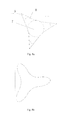
- FIG. 5 a is a schematic view of a mask plate including a square via hole pattern composed of four isosceles triangular protruding portions as provided by an embodiment of present invention
- FIG. 5 b illustrates a via hole profile formed upon exposure of the mask plate in FIG. 5 a
- FIG. 6 a is a schematic view of a mask plate including a square via hole pattern composed of four oval protruding portions as provided by an embodiment of present invention
- FIG. 6 b illustrates a via hole profile formed upon exposure of the mask plate in FIG. 6 a
- FIG. 7 a is a schematic view of a mask plate including a square via hole pattern composed of three isosceles trapezoidal protruding portions as provided by an embodiment of present invention
- FIG. 7 b illustrates a via hole profile formed upon exposure of the mask plate in FIG. 7 a
- FIG. 8 a is a schematic view of a mask plate including a square via hole pattern composed of three isosceles triangular protruding portions as provided by an embodiment of present invention
- FIG. 8 b illustrates a via hole profile formed upon exposure of the mask plate in FIG. 8 a
- FIG. 9 a is a schematic view of a mask plate including a square via hole pattern composed of three oval protruding portions as provided by an embodiment of present invention.
- FIG. 9 b illustrates a via hole profile formed upon exposure of the mask plate in FIG. 9 a.
- FIG. 1 illustrates a design concept of a via hole bridging a metal layer and an indium tin oxide (ITO) layer thereby achieving circuit conduction, wherein a metal layer 2 , a second insulating layer 3 and an ITO layer 4 arc stacked in this order on a first insulating layer 1 , and the second insulating layer 3 is provided with a via hole A (as indicated by the dashed box in FIG. 1 ) therein so as to bridge the metal layer 2 and the ITO layer 4 .
- ITO indium tin oxide
- the square via hole having a greater circumference and edge zone has smaller resistance while the circular via hole having smaller circumference and edge zone has larger resistance.
- FIGS. 2 a and 2 b illustrate a comparison diagram of the mask plate including a square via hole pattern before and after its exposure, wherein FIG. 2 a is the square via hole pattern before the exposure, and the FIG. 2 b is the via hole profile as formed after the exposure.
- the square via hole pattern forms a via hole of approximate circular shape after the exposure, and accordingly, its resistance will become greater; this is because an angular position has a smaller amount of transmitted light so that a photoresist corresponding to the angular position can not be exposed sufficiently, which makes it difficult to form an angular profile.
- FIG. 3 a illustrates a mask plate including an improved square via hole pattern
- FIG. 3 b illustrates a via hole as formed by the mask plate in FIG. 3 a upon exposure.
- FIG. 3 b tells that the improved design enhances the formation of angular profile of a via hole as compared with the normal design; however, a rounded profile at corners thereof substantively maintains unchanged, which still causes a greater via hole resistance as normally does.
- the inventor of the present application has realized that, given the same via hole area, the key to reduce the via hole resistance is to increase the circumference.
- an embodiment of the present invention provides a mask plate including a via hole pattern, the via hole pattern includes a body portion 7 and at least two protruding portions extending outward from the body portion 7 ; wherein a dimension of the body portion 7 is greater than a resolution dimension of an exposure machine as used, and each of the protruding portion includes a first protruding portion 8 with a dimension greater than the resolution dimension of the exposure machine.
- the mask plate provided by this embodiment has a via hole pattern including the body portion 7 and at least two protruding portions extending outward from the body portion 7 , so that the protruding portions themselves and zones between adjacent protruding portions, upon exposure by the exposure machine, will form convex portions and concave portions of a resulting via hole respectively, as illustrated in FIG. 4 b , thereby increasing a circumference of the resulting via hole, enlarging an area of edge zone of the resulting via hole and effectively reducing the resistance of the resulting via hole.
- each of the protruding portions of the via hole pattern further includes a second protruding portion 9 away from the body portion 7 , and a dimension of the second protruding portion 9 is smaller than the resolution dimension of the exposure machine. In this way, during exposure, an amount of transmitted light at the first protruding portion 8 with greater dimension than the exposure machine is further increased.
- FIGS. 4 a , 5 a , 6 a , 7 a , 8 a and 9 a three or four protruding portions are provided.
- the number of the protruding portions provided in these examples is configured for purpose of facilitating manufacturing process of the mask plate only and can be otherwise adjusted to further increase the circumference of the resulting via hole without particularly limited herein.
- the via holes formed upon exposing the via hole patterns as illustrated in FIGS. 4 a , 5 a , 6 a , 7 a , 8 a and 9 a are illustrated in FIGS. 4 b , 5 b , 6 b , 7 b , 8 b and 9 b , respectively.
- the protruding portions have equal, included angles therebetween. It should be understood that these equal, included angles ensure a uniform distribution of convex portions at a peripheral region of the via hole as formed upon exposure of the via hole pattern and hence to increase the circumference of the via hole while ensuring a convenience in manufacturing process. Still, as illustrated in FIGS. 4 b , 5 b , 6 b , 7 b , 8 b and 9 b , plural convex portions are distributed evenly at the peripheral region of the via hole as formed upon exposure.
- three protruding portions are provided for the via hole pattern, and the included angles between the three protruding portions are 120°.
- four protruding portions are provided for the via hole pattern, and the included angles between the four protruding portions arc 90°.
- the protruding portions have identical shapes and dimensions. In this way, it facilitates the manufacturing process of the mask plate.
- each of the protruding portions has a shape of any one of isosceles trapezoid, isosceles triangle and oval.
- the second protruding portion 9 and the first protruding portion 8 can be easily contained in a single pattern simultaneously, and a dimension gradually varied from the first protruding portion 8 to the second protruding portion 9 can also be provided, thereby ensuring a continuity of the profile of the resulting via hole formed upon exposure.
- the isosceles trapezoidal-shaped protruding portion includes a first protruding portion 8 close to the body portion 7 and a second protruding portion 9 away from the body portion 7 .
- the isosceles triangular-shaped protruding portion includes a first protruding portion 8 close to the body portion 7 and a second protruding portion 9 away from the body portion 7 .
- the oval-shaped protruding portion further includes a first protruding portion 8 close to the body portion 7 and a second protruding portion 9 away from the body portion 7 .
- the protruding portion of the via hole pattern has a portion with a greater dimension disposed to be close to the body portion 7 and a portion with a smaller dimension disposed to be away from the body portion 7 .
- the dimension of the protruding portion can be configured to be tapered from the portion close to the body portion 7 to the portion away from the body portion 7 .
- the body portion 7 and each of the protruding portion have their edges matching with each other. In this way, a location where the body portion 7 meshes with the protruding portion is relatively smooth, which allows a profile of the via hole as formed upon exposure smooth.
- a square equivalent to the via hole pattern has its side length in a range of 3 to 15 ⁇ m. As illustrated in FIG. 4 a , the square indicated by the dashed line is just the square equivalent to the via hole pattern and has its side length in an extent adapted to requirements of most of the pattern designs and manufacturing technologies.
Landscapes
- Physics & Mathematics (AREA)
- General Physics & Mathematics (AREA)
- Preparing Plates And Mask In Photomechanical Process (AREA)
- Electron Beam Exposure (AREA)
Abstract
Description
Claims (14)
Applications Claiming Priority (3)
| Application Number | Priority Date | Filing Date | Title |
|---|---|---|---|
| CN201510714183.8A CN105159025B (en) | 2015-10-29 | 2015-10-29 | a mask |
| CN201510714183 | 2015-10-29 | ||
| CN201510714183.8 | 2015-10-29 |
Publications (2)
| Publication Number | Publication Date |
|---|---|
| US20170123307A1 US20170123307A1 (en) | 2017-05-04 |
| US10101649B2 true US10101649B2 (en) | 2018-10-16 |
Family
ID=54799915
Family Applications (1)
| Application Number | Title | Priority Date | Filing Date |
|---|---|---|---|
| US15/298,376 Active 2036-12-09 US10101649B2 (en) | 2015-10-29 | 2016-10-20 | Mask plate |
Country Status (2)
| Country | Link |
|---|---|
| US (1) | US10101649B2 (en) |
| CN (1) | CN105159025B (en) |
Families Citing this family (2)
| Publication number | Priority date | Publication date | Assignee | Title |
|---|---|---|---|---|
| US9927698B2 (en) * | 2016-08-11 | 2018-03-27 | Globalfoundries Inc. | Dual exposure patterning of a photomask to print a contact, a via or curvilinear shape on an integrated circuit |
| CN107247386A (en) * | 2017-06-14 | 2017-10-13 | 京东方科技集团股份有限公司 | Mask plate, the forming method of via and display base plate, display base plate and device |
Citations (1)
| Publication number | Priority date | Publication date | Assignee | Title |
|---|---|---|---|---|
| US20060147813A1 (en) * | 2005-01-03 | 2006-07-06 | Tan Sya K | Mask and method to pattern chromeless phase lithography contact hole |
Family Cites Families (2)
| Publication number | Priority date | Publication date | Assignee | Title |
|---|---|---|---|---|
| CN103633027B (en) * | 2012-08-23 | 2016-12-21 | 中芯国际集成电路制造(上海)有限公司 | A kind of method forming the double epitaxial layer of source-drain area |
| CN103412462B (en) * | 2013-07-26 | 2016-03-02 | 北京京东方光电科技有限公司 | A kind of mask plate and liquid crystal panel |
-
2015
- 2015-10-29 CN CN201510714183.8A patent/CN105159025B/en not_active Expired - Fee Related
-
2016
- 2016-10-20 US US15/298,376 patent/US10101649B2/en active Active
Patent Citations (1)
| Publication number | Priority date | Publication date | Assignee | Title |
|---|---|---|---|---|
| US20060147813A1 (en) * | 2005-01-03 | 2006-07-06 | Tan Sya K | Mask and method to pattern chromeless phase lithography contact hole |
Also Published As
| Publication number | Publication date |
|---|---|
| US20170123307A1 (en) | 2017-05-04 |
| CN105159025A (en) | 2015-12-16 |
| CN105159025B (en) | 2019-07-23 |
Similar Documents
| Publication | Publication Date | Title |
|---|---|---|
| US11226550B2 (en) | Mask plate, method for forming via-hole, method for forming display substrate, the display substrate, and display device | |
| CN104407742B (en) | Touch base plate and preparation method thereof, display device | |
| JP7096257B2 (en) | Touch board and display device | |
| KR101910306B1 (en) | Mutual capacitance type ogs touch panel and manufacturing method therefor | |
| CN103296033B (en) | A kind of array base palte and preparation method thereof | |
| CN108170323B (en) | Display panels and display devices | |
| KR20220133833A (en) | Touch Panel | |
| CN109947305B (en) | Touch panel, preparation method thereof and touch display device | |
| US20210365151A1 (en) | Touch substrate, method of manufacturing the same, and touch apparatus | |
| US20150114815A1 (en) | Touch panel and method for manufacturing the same | |
| US10101649B2 (en) | Mask plate | |
| US20190101819A1 (en) | Mask plate | |
| US20150029411A1 (en) | Touch panel, conductive film and method for manufacturing the same | |
| US20180301467A1 (en) | Array substrate and display device | |
| US20220214767A9 (en) | Touch substrate and method for manufacturing the same | |
| CN108010445A (en) | Flexible Displays cover board and preparation method thereof, display device | |
| CN103412462B (en) | A kind of mask plate and liquid crystal panel | |
| CN106019733A (en) | Array substrate, display panel and display device | |
| CN108461505A (en) | Array substrate and preparation method thereof, display panel | |
| CN107577375A (en) | Touch-screen and its manufacture method | |
| WO2016165253A1 (en) | Array substrate and display device | |
| US20190012025A1 (en) | Touch Screen, Display Panel, and Display Device | |
| CN104766819B (en) | Pixel substrate and manufacturing method thereof | |
| US20220075467A1 (en) | Touch display panel and touch display device | |
| CN104317457B (en) | Bridging structure and contact panel for contact panel |
Legal Events
| Date | Code | Title | Description |
|---|---|---|---|
| AS | Assignment |
Owner name: CHONGQING BOE OPTOELECTRONICS TECHNOLOGY CO., LTD. Free format text: ASSIGNMENT OF ASSIGNORS INTEREST;ASSIGNOR:XU, ZHUO;REEL/FRAME:040073/0424 Effective date: 20160530 Owner name: CHONGQING BOE OPTOELECTRONICS TECHNOLOGY CO., LTD. Free format text: ASSIGNMENT OF ASSIGNORS INTEREST;ASSIGNOR:BAI, YAJIE;REEL/FRAME:040073/0512 Effective date: 20160530 Owner name: CHONGQING BOE OPTOELECTRONICS TECHNOLOGY CO., LTD. Free format text: ASSIGNMENT OF ASSIGNORS INTEREST;ASSIGNOR:KIM, JAIKWANG;REEL/FRAME:040073/0672 Effective date: 20160531 Owner name: CHONGQING BOE OPTOELECTRONICS TECHNOLOGY CO., LTD. Free format text: ASSIGNMENT OF ASSIGNORS INTEREST;ASSIGNOR:SHANG, FEI;REEL/FRAME:040073/0839 Effective date: 20160530 Owner name: BOE TECHNOLOGY GROUP CO., LTD., CHINA Free format text: ASSIGNMENT OF ASSIGNORS INTEREST;ASSIGNOR:KIM, JAIKWANG;REEL/FRAME:040073/0672 Effective date: 20160531 Owner name: BOE TECHNOLOGY GROUP CO., LTD., CHINA Free format text: ASSIGNMENT OF ASSIGNORS INTEREST;ASSIGNOR:BAI, YAJIE;REEL/FRAME:040073/0512 Effective date: 20160530 Owner name: BOE TECHNOLOGY GROUP CO., LTD., CHINA Free format text: ASSIGNMENT OF ASSIGNORS INTEREST;ASSIGNOR:SHANG, FEI;REEL/FRAME:040073/0839 Effective date: 20160530 Owner name: BOE TECHNOLOGY GROUP CO., LTD., CHINA Free format text: ASSIGNMENT OF ASSIGNORS INTEREST;ASSIGNOR:XU, ZHUO;REEL/FRAME:040073/0424 Effective date: 20160530 Owner name: CHONGQING BOE OPTOELECTRONICS TECHNOLOGY CO., LTD. Free format text: ASSIGNMENT OF ASSIGNORS INTEREST;ASSIGNOR:WANG, XIAOYUAN;REEL/FRAME:040427/0013 Effective date: 20160530 Owner name: BOE TECHNOLOGY GROUP CO., LTD., CHINA Free format text: ASSIGNMENT OF ASSIGNORS INTEREST;ASSIGNOR:WANG, XIAOYUAN;REEL/FRAME:040427/0013 Effective date: 20160530 |
|
| STCF | Information on status: patent grant |
Free format text: PATENTED CASE |
|
| MAFP | Maintenance fee payment |
Free format text: PAYMENT OF MAINTENANCE FEE, 4TH YEAR, LARGE ENTITY (ORIGINAL EVENT CODE: M1551); ENTITY STATUS OF PATENT OWNER: LARGE ENTITY Year of fee payment: 4 |