US10096579B2 - Thermal pads between stacked semiconductor dies and associated systems and methods - Google Patents
Thermal pads between stacked semiconductor dies and associated systems and methods Download PDFInfo
- Publication number
- US10096579B2 US10096579B2 US15/683,336 US201715683336A US10096579B2 US 10096579 B2 US10096579 B2 US 10096579B2 US 201715683336 A US201715683336 A US 201715683336A US 10096579 B2 US10096579 B2 US 10096579B2
- Authority
- US
- United States
- Prior art keywords
- silicon material
- die
- tsv
- semiconductor die
- thermal pad
- Prior art date
- Legal status (The legal status is an assumption and is not a legal conclusion. Google has not performed a legal analysis and makes no representation as to the accuracy of the status listed.)
- Active, expires
Links
Images


Classifications
-
- H10W90/00—
-
- H—ELECTRICITY
- H01—ELECTRIC ELEMENTS
- H01L—SEMICONDUCTOR DEVICES NOT COVERED BY CLASS H10
- H01L25/00—Assemblies consisting of a plurality of semiconductor or other solid state devices
- H01L25/03—Assemblies consisting of a plurality of semiconductor or other solid state devices all the devices being of a type provided for in a single subclass of subclasses H10B, H10D, H10F, H10H, H10K or H10N, e.g. assemblies of rectifier diodes
- H01L25/04—Assemblies consisting of a plurality of semiconductor or other solid state devices all the devices being of a type provided for in a single subclass of subclasses H10B, H10D, H10F, H10H, H10K or H10N, e.g. assemblies of rectifier diodes the devices not having separate containers
- H01L25/065—Assemblies consisting of a plurality of semiconductor or other solid state devices all the devices being of a type provided for in a single subclass of subclasses H10B, H10D, H10F, H10H, H10K or H10N, e.g. assemblies of rectifier diodes the devices not having separate containers the devices being of a type provided for in group H10D89/00
- H01L25/0657—Stacked arrangements of devices
-
- H—ELECTRICITY
- H01—ELECTRIC ELEMENTS
- H01L—SEMICONDUCTOR DEVICES NOT COVERED BY CLASS H10
- H01L24/00—Arrangements for connecting or disconnecting semiconductor or solid-state bodies; Methods or apparatus related thereto
- H01L24/01—Means for bonding being attached to, or being formed on, the surface to be connected, e.g. chip-to-package, die-attach, "first-level" interconnects; Manufacturing methods related thereto
- H01L24/02—Bonding areas ; Manufacturing methods related thereto
- H01L24/03—Manufacturing methods
-
- H—ELECTRICITY
- H01—ELECTRIC ELEMENTS
- H01L—SEMICONDUCTOR DEVICES NOT COVERED BY CLASS H10
- H01L24/00—Arrangements for connecting or disconnecting semiconductor or solid-state bodies; Methods or apparatus related thereto
- H01L24/01—Means for bonding being attached to, or being formed on, the surface to be connected, e.g. chip-to-package, die-attach, "first-level" interconnects; Manufacturing methods related thereto
- H01L24/02—Bonding areas ; Manufacturing methods related thereto
- H01L24/04—Structure, shape, material or disposition of the bonding areas prior to the connecting process
- H01L24/06—Structure, shape, material or disposition of the bonding areas prior to the connecting process of a plurality of bonding areas
-
- H—ELECTRICITY
- H01—ELECTRIC ELEMENTS
- H01L—SEMICONDUCTOR DEVICES NOT COVERED BY CLASS H10
- H01L25/00—Assemblies consisting of a plurality of semiconductor or other solid state devices
- H01L25/50—Multistep manufacturing processes of assemblies consisting of devices, the devices being individual devices of subclass H10D or integrated devices of class H10
-
- H10W20/023—
-
- H10W20/0249—
-
- H10W20/20—
-
- H10W40/228—
-
- H10W72/019—
-
- H—ELECTRICITY
- H01—ELECTRIC ELEMENTS
- H01L—SEMICONDUCTOR DEVICES NOT COVERED BY CLASS H10
- H01L2224/00—Indexing scheme for arrangements for connecting or disconnecting semiconductor or solid-state bodies and methods related thereto as covered by H01L24/00
- H01L2224/01—Means for bonding being attached to, or being formed on, the surface to be connected, e.g. chip-to-package, die-attach, "first-level" interconnects; Manufacturing methods related thereto
- H01L2224/02—Bonding areas; Manufacturing methods related thereto
- H01L2224/04—Structure, shape, material or disposition of the bonding areas prior to the connecting process
- H01L2224/0401—Bonding areas specifically adapted for bump connectors, e.g. under bump metallisation [UBM]
-
- H—ELECTRICITY
- H01—ELECTRIC ELEMENTS
- H01L—SEMICONDUCTOR DEVICES NOT COVERED BY CLASS H10
- H01L2224/00—Indexing scheme for arrangements for connecting or disconnecting semiconductor or solid-state bodies and methods related thereto as covered by H01L24/00
- H01L2224/01—Means for bonding being attached to, or being formed on, the surface to be connected, e.g. chip-to-package, die-attach, "first-level" interconnects; Manufacturing methods related thereto
- H01L2224/02—Bonding areas; Manufacturing methods related thereto
- H01L2224/04—Structure, shape, material or disposition of the bonding areas prior to the connecting process
- H01L2224/05—Structure, shape, material or disposition of the bonding areas prior to the connecting process of an individual bonding area
- H01L2224/05001—Internal layers
- H01L2224/0502—Disposition
- H01L2224/05025—Disposition the internal layer being disposed on a via connection of the semiconductor or solid-state body
-
- H—ELECTRICITY
- H01—ELECTRIC ELEMENTS
- H01L—SEMICONDUCTOR DEVICES NOT COVERED BY CLASS H10
- H01L2224/00—Indexing scheme for arrangements for connecting or disconnecting semiconductor or solid-state bodies and methods related thereto as covered by H01L24/00
- H01L2224/01—Means for bonding being attached to, or being formed on, the surface to be connected, e.g. chip-to-package, die-attach, "first-level" interconnects; Manufacturing methods related thereto
- H01L2224/02—Bonding areas; Manufacturing methods related thereto
- H01L2224/04—Structure, shape, material or disposition of the bonding areas prior to the connecting process
- H01L2224/05—Structure, shape, material or disposition of the bonding areas prior to the connecting process of an individual bonding area
- H01L2224/05001—Internal layers
- H01L2224/05099—Material
- H01L2224/051—Material with a principal constituent of the material being a metal or a metalloid, e.g. boron [B], silicon [Si], germanium [Ge], arsenic [As], antimony [Sb], tellurium [Te] and polonium [Po], and alloys thereof
- H01L2224/05138—Material with a principal constituent of the material being a metal or a metalloid, e.g. boron [B], silicon [Si], germanium [Ge], arsenic [As], antimony [Sb], tellurium [Te] and polonium [Po], and alloys thereof the principal constituent melting at a temperature of greater than or equal to 950°C and less than 1550°C
- H01L2224/05147—Copper [Cu] as principal constituent
-
- H—ELECTRICITY
- H01—ELECTRIC ELEMENTS
- H01L—SEMICONDUCTOR DEVICES NOT COVERED BY CLASS H10
- H01L2224/00—Indexing scheme for arrangements for connecting or disconnecting semiconductor or solid-state bodies and methods related thereto as covered by H01L24/00
- H01L2224/01—Means for bonding being attached to, or being formed on, the surface to be connected, e.g. chip-to-package, die-attach, "first-level" interconnects; Manufacturing methods related thereto
- H01L2224/02—Bonding areas; Manufacturing methods related thereto
- H01L2224/04—Structure, shape, material or disposition of the bonding areas prior to the connecting process
- H01L2224/06—Structure, shape, material or disposition of the bonding areas prior to the connecting process of a plurality of bonding areas
- H01L2224/0651—Function
- H01L2224/06515—Bonding areas having different functions
- H01L2224/06519—Bonding areas having different functions including bonding areas providing primarily thermal dissipation
-
- H—ELECTRICITY
- H01—ELECTRIC ELEMENTS
- H01L—SEMICONDUCTOR DEVICES NOT COVERED BY CLASS H10
- H01L2225/00—Details relating to assemblies covered by the group H01L25/00 but not provided for in its subgroups
- H01L2225/03—All the devices being of a type provided for in the same main group of the same subclass of class H10, e.g. assemblies of rectifier diodes
- H01L2225/04—All the devices being of a type provided for in the same main group of the same subclass of class H10, e.g. assemblies of rectifier diodes the devices not having separate containers
- H01L2225/065—All the devices being of a type provided for in the same main group of the same subclass of class H10
- H01L2225/06503—Stacked arrangements of devices
- H01L2225/06513—Bump or bump-like direct electrical connections between devices, e.g. flip-chip connection, solder bumps
-
- H—ELECTRICITY
- H01—ELECTRIC ELEMENTS
- H01L—SEMICONDUCTOR DEVICES NOT COVERED BY CLASS H10
- H01L2225/00—Details relating to assemblies covered by the group H01L25/00 but not provided for in its subgroups
- H01L2225/03—All the devices being of a type provided for in the same main group of the same subclass of class H10, e.g. assemblies of rectifier diodes
- H01L2225/04—All the devices being of a type provided for in the same main group of the same subclass of class H10, e.g. assemblies of rectifier diodes the devices not having separate containers
- H01L2225/065—All the devices being of a type provided for in the same main group of the same subclass of class H10
- H01L2225/06503—Stacked arrangements of devices
- H01L2225/06541—Conductive via connections through the device, e.g. vertical interconnects, through silicon via [TSV]
-
- H—ELECTRICITY
- H01—ELECTRIC ELEMENTS
- H01L—SEMICONDUCTOR DEVICES NOT COVERED BY CLASS H10
- H01L2225/00—Details relating to assemblies covered by the group H01L25/00 but not provided for in its subgroups
- H01L2225/03—All the devices being of a type provided for in the same main group of the same subclass of class H10, e.g. assemblies of rectifier diodes
- H01L2225/04—All the devices being of a type provided for in the same main group of the same subclass of class H10, e.g. assemblies of rectifier diodes the devices not having separate containers
- H01L2225/065—All the devices being of a type provided for in the same main group of the same subclass of class H10
- H01L2225/06503—Stacked arrangements of devices
- H01L2225/06589—Thermal management, e.g. cooling
-
- H—ELECTRICITY
- H01—ELECTRIC ELEMENTS
- H01L—SEMICONDUCTOR DEVICES NOT COVERED BY CLASS H10
- H01L2924/00—Indexing scheme for arrangements or methods for connecting or disconnecting semiconductor or solid-state bodies as covered by H01L24/00
- H01L2924/01—Chemical elements
- H01L2924/01022—Titanium [Ti]
-
- H—ELECTRICITY
- H01—ELECTRIC ELEMENTS
- H01L—SEMICONDUCTOR DEVICES NOT COVERED BY CLASS H10
- H01L2924/00—Indexing scheme for arrangements or methods for connecting or disconnecting semiconductor or solid-state bodies as covered by H01L24/00
- H01L2924/01—Chemical elements
- H01L2924/01074—Tungsten [W]
-
- H—ELECTRICITY
- H01—ELECTRIC ELEMENTS
- H01L—SEMICONDUCTOR DEVICES NOT COVERED BY CLASS H10
- H01L2924/00—Indexing scheme for arrangements or methods for connecting or disconnecting semiconductor or solid-state bodies as covered by H01L24/00
- H01L2924/06—Polymers
- H01L2924/07—Polyamine or polyimide
- H01L2924/07025—Polyimide
-
- H—ELECTRICITY
- H01—ELECTRIC ELEMENTS
- H01L—SEMICONDUCTOR DEVICES NOT COVERED BY CLASS H10
- H01L2924/00—Indexing scheme for arrangements or methods for connecting or disconnecting semiconductor or solid-state bodies as covered by H01L24/00
- H01L2924/10—Details of semiconductor or other solid state devices to be connected
- H01L2924/102—Material of the semiconductor or solid state bodies
- H01L2924/1025—Semiconducting materials
- H01L2924/10251—Elemental semiconductors, i.e. Group IV
- H01L2924/10253—Silicon [Si]
-
- H10W72/221—
-
- H10W72/227—
-
- H10W72/242—
-
- H10W72/244—
-
- H10W72/247—
-
- H10W72/265—
-
- H10W72/267—
-
- H10W72/29—
-
- H10W72/923—
-
- H10W72/942—
-
- H10W72/944—
-
- H10W72/952—
-
- H10W72/965—
-
- H10W72/967—
-
- H10W90/288—
-
- H10W90/297—
-
- H10W90/722—
Definitions
- the present technology generally relates to stacked semiconductor dies having through-silicon vias (TSVs).
- TSVs through-silicon vias
- Several embodiments of the present technology are related to improving heat dissipation of the stacked semiconductor dies by including metallic thermal pads between the dies in the stack.
- Stacked semiconductor dies are used in a wide variety of applications that require high data transfer rates and/or small footprints.
- many systems require a processor die (e.g., logic die) and one or more memory dies.
- the processor and memory dies are packaged in separate packages and are electrically interconnected through a motherboard.
- the processor and memory dies are placed next to each other on a common packaging substrate that provides electrical connectivity between the processor and memory dies. Nonetheless, in such applications a relatively large distance from one die to another limits the data transfer rates among the dies.
- the data transfer rates are additionally limited by the capacitance and inductance of the traces that electrically interconnect the dies.
- each die e.g., a processor or a memory die
- a processor and several memory dies can be stacked vertically and electrically interconnected using TSVs.
- the TSVs enable stacked dies to be stacked close to each other such that the dies are spaced apart from each other by only relatively small vertical distances, which in combination with the relatively low inductance of the TSVs enables higher data transfer rates. Also, since the dies are stacked vertically, the total footprint of the stack corresponds to the footprint of the largest die in the stack.
- FIG. 1 is a partially schematic cross-sectional view of a vertically stacked die arrangement in accordance with the prior art.
- a stacked die assembly 1000 has a processor die 110 , three memory dies 120 a - c stacked on the processor die 110 , and TSVs 150 that electrically connect the processor die 110 with the memory dies 120 a - c .
- the processor die 110 can have several functional areas, for example a processor core 116 , read/write logic 117 and/or I/O buffer 118 . These functional areas can be electrically interconnected through metallization traces 119 .
- the processor die 110 also includes pads 115 for electrically connecting the stacked die assembly 1000 to a package substrate (not shown) through, for example, wirebonds.
- the closely spaced, vertically stacked dies 110 and 120 a - c are suitable for relatively high data transfer rates while occupying only a relatively small total area.
- the close spacing of the semiconductor dies also increases the density of power dissipated by the semiconductor dies. Therefore, thermal management is typically more difficult for stacked semiconductor dies than for other arrangements.
- One possible improvement in the thermal management of the stacked semiconductor dies includes placing thermal pads (dummy pads, outrigger pads) between the dies in the stack to enhance heat transfer through and ultimately out of the stack.
- FIGS. 2A-2G illustrate a manufacturing process for thermal pads of a semiconductor die stack in accordance with the prior art.
- FIG. 2A illustrates a semiconductor die 201 attached to a carrier wafer 225 by an adhesive 220 .
- the carrier wafer 225 can be used to improve handling and to protect the semiconductor dies during the manufacturing process. Suitable carrier materials are, for example, ceramic or silicon. In a typical semiconductor manufacturing process, the carrier wafer will be removed from the semiconductor dies before packaging the individual semiconductor dies.
- the semiconductor die 201 can have a silicon material 210 , an active structure 215 that includes electrical circuits, and TSVs 230 interconnecting the electrical circuits of the active structure 215 to an area at a peripheral surface 211 of the silicon material 210 . As explained in relation to FIG.
- the peripheral surface 211 faces additional die or dies in the stack.
- the die 210 can also have an isolation lining 235 ( FIGS. 2A-2C ) that electrically isolates a conductive material 231 of the TSV 230 from the silicon material 210 . Only one TSV 230 is shown in FIG. 2A for clarity, but a typical semiconductor die would include many TSVs.
- FIG. 2B illustrates the semiconductor die 201 after planarizing or grinding the peripheral surface 211 . This can thin the die and roughen the peripheral surface 211 , which improves adhesion of mask layers used in subsequent processing steps.
- FIG. 2C illustrates the semiconductor die 201 after the peripheral surface 211 has been etched to expose one end portion of the TSV 230 .
- Suitable silicon etching techniques include, for example, selectively etching silicon while not etching metals, for example copper. After etching, a portion of the TSV 230 projects above the peripheral surface 211 of the semiconductor die 201 .
- FIGS. 2D and 2E illustrate the semiconductor die 201 with a passivation material 280 before and after patterning, respectively.
- the passivation material 280 can be a polymer, for example, a polyimide.
- Suitable patterning techniques include, for example, photo patterning and developing a resist material to etch indentations 285 in the passivation material 280 .
- a leaky chrome process can be used to pattern the indentations 285 .
- the indentations 285 in the passivation material 280 provide locations for subsequent metal deposition.
- sputtering techniques can be used to deposit metal into the indentations 285 .
- FIG. 2F illustrates the semiconductor die 201 after depositing metal into the indentations 285 to form thermal pads 250 and an under-bump metallization (UBM) structure 255 .
- the thermal pads 250 and UBM structure 255 are formed during the same metal deposition process.
- the thermal pads 250 have a relatively high thermal conductivity that improves heat dissipation from the semiconductor die 201 when the thermal pads 250 contact the next semiconductor die in the stack.
- the thermal pads 250 transfer heat through the stack and ultimately to the environment.
- the UBM structure 255 that caps the exposed end of the TSV 230 electrically connects signal, power and/or ground lines with other semiconductor dies in the stack.
- the thermal pads 250 are formed over a thin portion of the passivation material 280 that separates the thermal pads 250 from the silicon material 210 by a thickness T. Additionally, since the thermal pads 250 and UBM structure 255 are formed in a same semiconductor manufacturing step (e.g., metal deposition), approximately same thickness of material is added to the target areas of the semiconductor die corresponding to the pattern of indentations 285 . As such, after forming the UBM structures 255 and the thermal pads 250 , the top of the UBM structure 255 may be higher than the top of the thermal pad. For example, the top of the UBM structure 255 may be separated from the top of the thermal pad 250 by a distance L.
- FIG. 2G illustrates stacking of the semiconductor dies 201 and 202 stacked after the carrier wafer 225 and adhesive 220 have been removed.
- the semiconductor dies 201 and 202 are aligned such that the TSV 230 of the semiconductor die 201 connects to a TSV 232 of the semiconductor die 202 through a die pad 270 when the semiconductor dies are brought into contact in a direction of arrows 251 .
- the thermal pads 250 help to transfer heat Q from the stack in addition to the heat transferred through the TSV 230 .
- the illustrated conventional thermal pads 250 suffer from several deficiencies.
- the passivation material 280 (e.g., a polymer) has a relatively low thermal conductivity that inhibits heat transfer from the semiconductor die 202 in proportion to a thickness T of the passivation material that separates the thermal pads 250 from the silicon material 210 .
- the uneven height (e.g., distance L) of the UBM structure 255 and the thermal pads 250 generally reduces the stacking yield of the semiconductor dies because contact between the UBM structure 255 and the die pad 270 can prevent the thermal pads 250 from contacting the semiconductor die 202 .
- FIG. 1 is a partially schematic cross-sectional view of vertically stacked dies in accordance with the prior art.
- FIGS. 2A-2G illustrate a manufacturing process for forming thermal pads of a semiconductor die stack in accordance with the prior art.
- FIGS. 3A-3I illustrate a manufacturing process for forming thermal pads of a semiconductor die stack in accordance with an embodiment of the present technology.
- FIGS. 4A-4G illustrate a manufacturing process for forming thermal pads of a semiconductor die stack in accordance with another embodiment of the present technology.
- FIG. 5 is a comparison graph of die temperatures in conventional die stacks compared to embodiments of the present technology.
- the stacked die assemblies may include vertical stacks of memory dies, processor dies, and/or other dies that are electrically interconnected using through-substrate vias (TSVs).
- TSVs through-substrate vias
- thermal pads can contact the adjacent silicon dies in the stack to improve heat transfer through the semiconductor die stack.
- thermal pads having a relatively high thermal conductivity can directly contact the adjacent silicon dies in the stack without the intervening layers of the low thermal conductivity materials (e.g., passivation materials).
- the thermal pads and UBM structures of a semiconductor die can have generally coplanar top surfaces to improve adhesion of the thermal pads and UBM structures with the next die of the stack and thereby improve the overall die stacking yield (e.g., manufacturing yield).
- FIGS. 3A-3I illustrate a manufacturing process for forming thermal pads of a semiconductor die stack in accordance with an embodiment of the present technology.
- FIG. 3A illustrates a semiconductor die 301 having a silicon material 310 with a peripheral surface 311 and an active structure 315 .
- the semiconductor die 301 can be attached to a carrier wafer 325 by an adhesive 320 .
- the carrier wafer 325 can be used for improved handling and protection of the semiconductor dies during the manufacturing process, and the carrier wafer 325 can be removed from the semiconductor die 301 before packaging the individual semiconductor dies in a stack.
- the die 301 can also include a plurality of TSVs 330 (only one shown) that electrically connect integrated circuits of the active structure 315 with other semiconductor dies in the stack, and each TSV 330 can have a conductive material 331 and an isolation lining 335 that electrically isolates the conductive material 331 from the silicon material 310 .
- FIG. 3B illustrates the semiconductor die 301 after planarizing the peripheral surface 311 and the top of the TSV 330 .
- the planarization thins the die to reduce the overall height of the die stack. Additionally, the planarization can roughen the peripheral surface 311 to improve adhesion of the mask layers and metallization of the subsequent manufacturing steps.
- Suitable planarization and grinding techniques include, for example, chemical-mechanical planarization and mechanical grinding.
- FIG. 3C illustrates the semiconductor die 301 after applying a mask 390 over the peripheral surface 311 and forming an opening 395 in the mask 390 aligned with the TSV 330 .
- the opening 395 exposes the TSV 330 and a portion of the peripheral surface 311 around the TSV 330 (e.g., laterally from the TSV 330 ).
- the exposed portion of the peripheral surface 311 can be etched while the remaining areas of the peripheral surface 311 covered by the mask 390 are protected from the etchant.
- FIG. 3D illustrates the semiconductor die 301 after the silicon material 310 around the TSV 330 has been etched to form an indentation 345 .
- Suitable silicon etchants can selectively etch the silicon material 310 while not etching the conductive material 331 of the TSV 330 or at least etching the conductive material 331 at a slower rate than that of the silicon material 310 .
- a non-isotropic etchant can create inclined surfaces of the indentation 345 , but isotropic etchants can also be used. After etching a portion of the silicon material 310 around the TSV 330 , the TSV 330 projects above the floor of the indentation 345 .
- the exposed end of the TSV 330 can be generally co-planar with the areas of peripheral surface 311 covered by the mask 390 ( FIG. 3C ), which can promote a generally uniform height of a subsequently deposited metal material as explained in more detail with reference to FIGS. 3G and 3H below.
- FIGS. 3E and 3F illustrate the semiconductor die 301 after a passivation material 380 has been deposited ( FIG. 3E ) and then patterned ( FIG. 3F ).
- the passivation material 380 covers the peripheral surface 311 of the semiconductor die 301 , but does not cover the top of the TSV 330 .
- Suitable passivation materials may include polyimide or nitrogen oxide. In some embodiments, the passivation material can have a thickness of about 2 ⁇ m.
- the passivation material 380 has openings 385 ( FIG. 3F ) that expose locations for metal deposition on or otherwise at the peripheral surface 311 .
- FIG. 3G illustrates the semiconductor die 301 after thermal pads 350 and UBM structures 355 (only one shown) have been formed.
- the thermal pads 350 can be formed by depositing metal into the openings 385
- the UBM structure 355 can be formed by depositing metal over the exposed end of the TSV 330 .
- sputtering techniques can be used to deposit metal into the openings and over the exposed end of the TSV 330 in a single process.
- an adhesion material 352 e.g., Ti and/or TiW
- the top surfaces of the UBM structure 355 and the thermal pads 350 are generally coplanar (e.g., at generally the same height (H)) because the exposed end of the TSV 330 and the peripheral surface 311 are at least substantially coplanar at the onset of the metal deposition process.
- FIG. 3H shows the semiconductor die 310 after the carrier wafer 325 has been removed.
- coplanarity between the tops of the thermal pads 350 and UBM structures 355 can improve attachment of the semiconductor die 301 to the next semiconductor die in the stack.
- FIG. 3I illustrates stacking of the semiconductor dies 301 and 302 .
- the UBM structure 355 of the semiconductor die 301 can be aligned with a corresponding die pad 370 of the semiconductor die 302 .
- the thermal pads 350 of the semiconductor die 301 contact an active structure 316 of the semiconductor die 302
- the UBM structure 355 contacts the die pad 370 .
- heat transfer (Q) between the dies 301 , 302 (and ultimately away from the stack) can be improved by a relatively high thermal conductivity of the thermal pads 350 that directly contact semiconductor dies 301 and 302 .
- the thermal pads 350 can be formed of copper, aluminum and/or other metals. Furthermore, since the top surfaces of the thermal pads 350 and UBM structure 355 are at least substantially coplanar, the stacking yields of the semiconductor dies can be improved because of better alignment of the thermal pads 350 and UBM structure 355 with the corresponding structures of the semiconductor die 302 . Additional semiconductor dies (not shown) can also be added to the stack. For example, the stack can include 4, 8, 10, or more semiconductor dies.
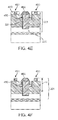
- FIGS. 4A-4G illustrate a manufacturing process for forming thermal pads of a semiconductor die stack in accordance with an additional embodiment of the present technology.
- FIG. 4A corresponds to FIG. 3C described above, and like reference number refer to the same or similar components in FIGS. 3A-4G .
- FIG. 4B illustrates the semiconductor die 301 after etching the exposed portion of the peripheral surface 311 to form an indentation 445 in the semiconductor material 310 around the exposed end of the TSV 330 .
- the indentation 445 is formed using an isotropic etchant that forms generally vertical walls in the silicon material 310 , but non-isotropic etchants can also be used.
- the etchant can selectively remove the silicon material 310 such that the TSV 330 remains substantially unchanged by etching. Therefore, the TSV 330 can have a top surface that is generally coplanar with the peripheral surface 311 of the silicon material 310 .
- FIGS. 4C and 4D illustrate the semiconductor die 301 after a passivation material 480 has been deposited ( FIG. 4C ) and then patterned ( FIG. 4D ).
- the passivation material 480 is patterned to have openings 485 that expose areas the peripheral surface 311 of the semiconductor material 310 to a subsequent metal deposition.
- FIG. 4E illustrates the semiconductor die 301 after thermal pads 450 have been formed in the openings 485 ( FIG. 4D ) of the passivation material 480 and UBM structure 455 has been formed on the TSV 330 .
- the thermal pads 450 and the UBM structure 455 can be formed concurrently such that they have approximately the same thickness. Since the exposed end of the TSV 330 (where the UBM structure 455 is formed) is generally coplanar with the peripheral surface 311 (where the thermal pads 450 are formed), the resulting vertical height of the UBM structure 455 and the thermal pads 450 can also be generally same, e.g., the UBM structure 455 and the thermal pads 450 can be at a generally same height (H).
- FIG. 4F illustrates the semiconductor die 301 after the passivation material around the thermal pads has been stripped away (e.g., by etching).
- FIG. 4G illustrates stacking of the semiconductor dies 301 and 302 where the semiconductor die 301 is made as shown in FIGS. 4A-4F .
- the thermal pads 450 and the UBM structure 455 of the semiconductor die 301 can contact the semiconductor die 302 at the active structure 316 and the die pad 370 , respectively, as indicated by arrows 451 .
- a direct contact between the thermal pads 450 and the active structure 316 improves heat transfer (Q) between the dies 301 and 302 due to a relatively high thermal conductivity of the thermal pads 450 that are in direct contact with semiconductor dies.
- the stacking yields of the semiconductor dies can be improved.
- the stacking process may be repeated for additional dies in the stack. However, in accordance with an embodiments of the present technology, only some dies in the stack may be directly contacted with the thermal pads 450 , while others are not.
- FIG. 5 is a comparison graph of die temperatures obtained by a numerical simulation of the conventional die stacks and die stacks in accordance with the present technology.
- Each simulation test case includes a semiconductor die stack having a logic semiconductor die and several memory dies.
- the horizontal axis includes three test cases: (a) a die stack having conventional thermal pad technology, (b) an embodiment of the present technology that includes thermal pads between the individual memory dies, and (c) an embodiment of the present technology that includes thermal pads between the individual memory dies and also between the logic die and the stack of the memory dies.
- the vertical axis indicates the maximum temperature simulated on the logic die and on the memory die that is next to the logic die.
- the thermal pads according to the present technology were used between all the dies in the stack (logic and memory, test case c), the heat dissipation from the stack was additionally improved and the temperatures simulated on the logic and memory dies were further lowered to 94° C. and 90.9° C., respectively. Therefore, the thermal pads according to the present technology produced lower temperature of the semiconductor dies in comparison to the conventional thermal pads in the same die stack.
- materials of the thermal pads can differ from the materials of the UBM structures.
- the heights of the thermal pads and the UBM structures can be different if the structures of the next die in the stack have correspondingly adjusted heights.
- a UBM structure that is higher than the thermal pads can be mated to a die pad that is recessed into an active surface of the next die by an appropriate depth, while still resulting in relatively good stacking yields.
Landscapes
- Engineering & Computer Science (AREA)
- Microelectronics & Electronic Packaging (AREA)
- Power Engineering (AREA)
- Computer Hardware Design (AREA)
- Physics & Mathematics (AREA)
- Condensed Matter Physics & Semiconductors (AREA)
- General Physics & Mathematics (AREA)
- Manufacturing & Machinery (AREA)
- Internal Circuitry In Semiconductor Integrated Circuit Devices (AREA)
- Chemical & Material Sciences (AREA)
- Materials Engineering (AREA)
Abstract
Description
Claims (17)
Priority Applications (4)
| Application Number | Priority Date | Filing Date | Title |
|---|---|---|---|
| US15/683,336 US10096579B2 (en) | 2014-02-03 | 2017-08-22 | Thermal pads between stacked semiconductor dies and associated systems and methods |
| US16/122,280 US10651155B2 (en) | 2014-02-03 | 2018-09-05 | Thermal pads between stacked semiconductor dies and associated systems and methods |
| US16/871,443 US12033980B2 (en) | 2014-02-03 | 2020-05-11 | Thermal pads between stacked semiconductor dies and associated systems and methods |
| US18/751,061 US20240347511A1 (en) | 2014-02-03 | 2024-06-21 | Thermal pads between stacked semiconductor dies and associated systems and methods |
Applications Claiming Priority (2)
| Application Number | Priority Date | Filing Date | Title |
|---|---|---|---|
| US14/171,169 US9768147B2 (en) | 2014-02-03 | 2014-02-03 | Thermal pads between stacked semiconductor dies and associated systems and methods |
| US15/683,336 US10096579B2 (en) | 2014-02-03 | 2017-08-22 | Thermal pads between stacked semiconductor dies and associated systems and methods |
Related Parent Applications (1)
| Application Number | Title | Priority Date | Filing Date |
|---|---|---|---|
| US14/171,169 Division US9768147B2 (en) | 2014-02-03 | 2014-02-03 | Thermal pads between stacked semiconductor dies and associated systems and methods |
Related Child Applications (1)
| Application Number | Title | Priority Date | Filing Date |
|---|---|---|---|
| US16/122,280 Continuation US10651155B2 (en) | 2014-02-03 | 2018-09-05 | Thermal pads between stacked semiconductor dies and associated systems and methods |
Publications (2)
| Publication Number | Publication Date |
|---|---|
| US20170352645A1 US20170352645A1 (en) | 2017-12-07 |
| US10096579B2 true US10096579B2 (en) | 2018-10-09 |
Family
ID=53755481
Family Applications (5)
| Application Number | Title | Priority Date | Filing Date |
|---|---|---|---|
| US14/171,169 Active US9768147B2 (en) | 2014-02-03 | 2014-02-03 | Thermal pads between stacked semiconductor dies and associated systems and methods |
| US15/683,336 Active 2034-02-10 US10096579B2 (en) | 2014-02-03 | 2017-08-22 | Thermal pads between stacked semiconductor dies and associated systems and methods |
| US16/122,280 Active US10651155B2 (en) | 2014-02-03 | 2018-09-05 | Thermal pads between stacked semiconductor dies and associated systems and methods |
| US16/871,443 Active US12033980B2 (en) | 2014-02-03 | 2020-05-11 | Thermal pads between stacked semiconductor dies and associated systems and methods |
| US18/751,061 Pending US20240347511A1 (en) | 2014-02-03 | 2024-06-21 | Thermal pads between stacked semiconductor dies and associated systems and methods |
Family Applications Before (1)
| Application Number | Title | Priority Date | Filing Date |
|---|---|---|---|
| US14/171,169 Active US9768147B2 (en) | 2014-02-03 | 2014-02-03 | Thermal pads between stacked semiconductor dies and associated systems and methods |
Family Applications After (3)
| Application Number | Title | Priority Date | Filing Date |
|---|---|---|---|
| US16/122,280 Active US10651155B2 (en) | 2014-02-03 | 2018-09-05 | Thermal pads between stacked semiconductor dies and associated systems and methods |
| US16/871,443 Active US12033980B2 (en) | 2014-02-03 | 2020-05-11 | Thermal pads between stacked semiconductor dies and associated systems and methods |
| US18/751,061 Pending US20240347511A1 (en) | 2014-02-03 | 2024-06-21 | Thermal pads between stacked semiconductor dies and associated systems and methods |
Country Status (1)
| Country | Link |
|---|---|
| US (5) | US9768147B2 (en) |
Families Citing this family (11)
| Publication number | Priority date | Publication date | Assignee | Title |
|---|---|---|---|---|
| WO2014183287A1 (en) * | 2013-05-16 | 2014-11-20 | Advanced Micro Devices, Inc. | Memory system with region-specific memory access scheduling |
| US9653442B2 (en) * | 2014-01-17 | 2017-05-16 | Taiwan Semiconductor Manufacturing Company, Ltd. | Integrated circuit package and methods of forming same |
| US9768147B2 (en) | 2014-02-03 | 2017-09-19 | Micron Technology, Inc. | Thermal pads between stacked semiconductor dies and associated systems and methods |
| US10256203B2 (en) * | 2017-07-27 | 2019-04-09 | Taiwan Semiconductor Manufacturing Co., Ltd. | Semiconductor device and semiconductor package |
| US20200006272A1 (en) * | 2018-06-29 | 2020-01-02 | Andreas Augustin | Through-silicon via pillars for connecting dice and methods of assembling same |
| KR102629405B1 (en) * | 2018-11-09 | 2024-01-25 | 삼성전자주식회사 | Memory devices, memory systems and methods of operating memory devices |
| US11581280B2 (en) * | 2019-12-27 | 2023-02-14 | Stmicroelectronics Pte Ltd | WLCSP package with different solder volumes |
| US11063012B1 (en) * | 2020-04-24 | 2021-07-13 | Nanya Technology Corporation | Semiconductor structure having buffer under bump pad and manufacturing method thereof |
| CN113964091A (en) | 2020-07-20 | 2022-01-21 | 长鑫存储技术有限公司 | Semiconductor device, manufacturing method thereof and three-dimensional integrated circuit |
| KR20230039214A (en) | 2021-09-14 | 2023-03-21 | 삼성전자주식회사 | Thermal pad, semiconductor chip including the same and method of manufacturing the semiconductor chip |
| KR20230052367A (en) | 2021-10-12 | 2023-04-20 | 삼성전자주식회사 | Semiconductor packages and method for manufacturing the same |
Citations (23)
| Publication number | Priority date | Publication date | Assignee | Title |
|---|---|---|---|---|
| US5424245A (en) | 1994-01-04 | 1995-06-13 | Motorola, Inc. | Method of forming vias through two-sided substrate |
| US5528080A (en) | 1993-03-05 | 1996-06-18 | Goldstein; Edward F. | Electrically conductive interconnection through a body of semiconductor material |
| US20040259325A1 (en) | 2003-06-19 | 2004-12-23 | Qing Gan | Wafer level chip scale hermetic package |
| US7109068B2 (en) | 2004-08-31 | 2006-09-19 | Micron Technology, Inc. | Through-substrate interconnect fabrication methods |
| US7179740B1 (en) | 1999-05-03 | 2007-02-20 | United Microelectronics Corporation | Integrated circuit with improved interconnect structure and process for making same |
| US20070045836A1 (en) | 2005-08-31 | 2007-03-01 | Samsung Electronics Co., Ltd. | Stacked chip package using warp preventing insulative material and manufacturing method thereof |
| US7387949B2 (en) | 2004-12-21 | 2008-06-17 | Seiko Epson Corporation | Semiconductor device manufacturing method, semiconductor device, laminated semiconductor device, circuit substrate, and electronic apparatus |
| US20090160050A1 (en) | 2005-08-26 | 2009-06-25 | Honda Motor Co., Ltd. | Semiconductor device manufacturing method, semiconductor device and wafer |
| US20090283898A1 (en) | 2008-05-15 | 2009-11-19 | Janzen Jeffery W | Disabling electrical connections using pass-through 3d interconnects and associated systems and methods |
| US20100171197A1 (en) | 2009-01-05 | 2010-07-08 | Hung-Pin Chang | Isolation Structure for Stacked Dies |
| US7786573B2 (en) | 2005-07-15 | 2010-08-31 | Samsung Electronics Co., Ltd. | Packaging chip having interconnection electrodes directly connected to plural wafers |
| US20100330798A1 (en) | 2009-06-26 | 2010-12-30 | Taiwan Semiconductor Manufacturing Company, Ltd. | Formation of TSV Backside Interconnects by Modifying Carrier Wafers |
| US8030780B2 (en) | 2008-10-16 | 2011-10-04 | Micron Technology, Inc. | Semiconductor substrates with unitary vias and via terminals, and associated systems and methods |
| US20110291265A1 (en) | 2010-05-27 | 2011-12-01 | Sin-Hyun Jin | Semiconductor integrated circuit having a multi-chip structure |
| US8159065B2 (en) | 2009-03-06 | 2012-04-17 | Hynix Semiconductor Inc. | Semiconductor package having an internal cooling system |
| US8395057B2 (en) | 2006-09-04 | 2013-03-12 | Nanospace Ab | Substrate-penetrating electrical connections |
| US20130157436A1 (en) | 2011-12-14 | 2013-06-20 | Sematech, Inc. | Forming through substrate vias |
| US20130168740A1 (en) * | 2012-01-02 | 2013-07-04 | Kun-Lung Chen | Integrated compact mems device with deep trench contacts |
| US20130193527A1 (en) * | 2012-01-31 | 2013-08-01 | Taiwan Semiconductor Manufacturing Company, Ltd. | Micro-electro mechanical system (mems) structures with through substrate vias and methods of forming the same |
| US20140027920A1 (en) | 2012-07-30 | 2014-01-30 | Fujitsu Semiconductor Limited | Semiconductor device and method for manufacturing the same |
| US20140197541A1 (en) | 2013-01-15 | 2014-07-17 | Freescale Semiconductor, Inc. | Microelectronic assembly having a heat spreader for a plurality of die |
| US20140239457A1 (en) | 2013-02-28 | 2014-08-28 | International Business Machines Corporation | Thermal via for 3d integrated circuits structures |
| US20150221612A1 (en) | 2014-02-03 | 2015-08-06 | Micron Technology, Inc. | Thermal pads between stacked semiconductor dies and associated systems and methods |
Family Cites Families (12)
| Publication number | Priority date | Publication date | Assignee | Title |
|---|---|---|---|---|
| SG111972A1 (en) * | 2002-10-17 | 2005-06-29 | Agency Science Tech & Res | Wafer-level package for micro-electro-mechanical systems |
| JP4415984B2 (en) * | 2006-12-06 | 2010-02-17 | ソニー株式会社 | Manufacturing method of semiconductor device |
| US8154134B2 (en) * | 2008-05-12 | 2012-04-10 | Texas Instruments Incorporated | Packaged electronic devices with face-up die having TSV connection to leads and die pad |
| US8399987B2 (en) * | 2009-12-04 | 2013-03-19 | Samsung Electronics Co., Ltd. | Microelectronic devices including conductive vias, conductive caps and variable thickness insulating layers |
| US8928159B2 (en) * | 2010-09-02 | 2015-01-06 | Taiwan Semiconductor Manufacturing & Company, Ltd. | Alignment marks in substrate having through-substrate via (TSV) |
| US8193039B2 (en) * | 2010-09-24 | 2012-06-05 | Advanced Micro Devices, Inc. | Semiconductor chip with reinforcing through-silicon-vias |
| US8900994B2 (en) * | 2011-06-09 | 2014-12-02 | Taiwan Semiconductor Manufacturing Company, Ltd. | Method for producing a protective structure |
| US9065358B2 (en) * | 2011-07-11 | 2015-06-23 | Taiwan Semiconductor Manufacturing Company, Ltd. | MEMS structure and method of forming same |
| US8466062B2 (en) * | 2011-11-02 | 2013-06-18 | Globalfoundries Singapore Pte Ltd | TSV backside processing using copper damascene interconnect technology |
| KR101870155B1 (en) * | 2012-02-02 | 2018-06-25 | 삼성전자주식회사 | Via Connection Structures and Semiconductor Devices Having the Same, and methods of Fabricating the Sames |
| US9269664B2 (en) * | 2012-04-10 | 2016-02-23 | Mediatek Inc. | Semiconductor package with through silicon via interconnect and method for fabricating the same |
| US20130299950A1 (en) * | 2012-05-11 | 2013-11-14 | Sematech, Inc. | Semiconductor structure with buried through substrate vias |
-
2014
- 2014-02-03 US US14/171,169 patent/US9768147B2/en active Active
-
2017
- 2017-08-22 US US15/683,336 patent/US10096579B2/en active Active
-
2018
- 2018-09-05 US US16/122,280 patent/US10651155B2/en active Active
-
2020
- 2020-05-11 US US16/871,443 patent/US12033980B2/en active Active
-
2024
- 2024-06-21 US US18/751,061 patent/US20240347511A1/en active Pending
Patent Citations (24)
| Publication number | Priority date | Publication date | Assignee | Title |
|---|---|---|---|---|
| US5528080A (en) | 1993-03-05 | 1996-06-18 | Goldstein; Edward F. | Electrically conductive interconnection through a body of semiconductor material |
| US5424245A (en) | 1994-01-04 | 1995-06-13 | Motorola, Inc. | Method of forming vias through two-sided substrate |
| US7179740B1 (en) | 1999-05-03 | 2007-02-20 | United Microelectronics Corporation | Integrated circuit with improved interconnect structure and process for making same |
| US20040259325A1 (en) | 2003-06-19 | 2004-12-23 | Qing Gan | Wafer level chip scale hermetic package |
| US7109068B2 (en) | 2004-08-31 | 2006-09-19 | Micron Technology, Inc. | Through-substrate interconnect fabrication methods |
| US7387949B2 (en) | 2004-12-21 | 2008-06-17 | Seiko Epson Corporation | Semiconductor device manufacturing method, semiconductor device, laminated semiconductor device, circuit substrate, and electronic apparatus |
| US7786573B2 (en) | 2005-07-15 | 2010-08-31 | Samsung Electronics Co., Ltd. | Packaging chip having interconnection electrodes directly connected to plural wafers |
| US20090160050A1 (en) | 2005-08-26 | 2009-06-25 | Honda Motor Co., Ltd. | Semiconductor device manufacturing method, semiconductor device and wafer |
| US20070045836A1 (en) | 2005-08-31 | 2007-03-01 | Samsung Electronics Co., Ltd. | Stacked chip package using warp preventing insulative material and manufacturing method thereof |
| US8395057B2 (en) | 2006-09-04 | 2013-03-12 | Nanospace Ab | Substrate-penetrating electrical connections |
| US20090283898A1 (en) | 2008-05-15 | 2009-11-19 | Janzen Jeffery W | Disabling electrical connections using pass-through 3d interconnects and associated systems and methods |
| US8030780B2 (en) | 2008-10-16 | 2011-10-04 | Micron Technology, Inc. | Semiconductor substrates with unitary vias and via terminals, and associated systems and methods |
| US20100171197A1 (en) | 2009-01-05 | 2010-07-08 | Hung-Pin Chang | Isolation Structure for Stacked Dies |
| US8159065B2 (en) | 2009-03-06 | 2012-04-17 | Hynix Semiconductor Inc. | Semiconductor package having an internal cooling system |
| US20100330798A1 (en) | 2009-06-26 | 2010-12-30 | Taiwan Semiconductor Manufacturing Company, Ltd. | Formation of TSV Backside Interconnects by Modifying Carrier Wafers |
| US20110291265A1 (en) | 2010-05-27 | 2011-12-01 | Sin-Hyun Jin | Semiconductor integrated circuit having a multi-chip structure |
| US20130157436A1 (en) | 2011-12-14 | 2013-06-20 | Sematech, Inc. | Forming through substrate vias |
| US8614145B2 (en) | 2011-12-14 | 2013-12-24 | Sematech, Inc. | Through substrate via formation processing using sacrificial material |
| US20130168740A1 (en) * | 2012-01-02 | 2013-07-04 | Kun-Lung Chen | Integrated compact mems device with deep trench contacts |
| US20130193527A1 (en) * | 2012-01-31 | 2013-08-01 | Taiwan Semiconductor Manufacturing Company, Ltd. | Micro-electro mechanical system (mems) structures with through substrate vias and methods of forming the same |
| US20140027920A1 (en) | 2012-07-30 | 2014-01-30 | Fujitsu Semiconductor Limited | Semiconductor device and method for manufacturing the same |
| US20140197541A1 (en) | 2013-01-15 | 2014-07-17 | Freescale Semiconductor, Inc. | Microelectronic assembly having a heat spreader for a plurality of die |
| US20140239457A1 (en) | 2013-02-28 | 2014-08-28 | International Business Machines Corporation | Thermal via for 3d integrated circuits structures |
| US20150221612A1 (en) | 2014-02-03 | 2015-08-06 | Micron Technology, Inc. | Thermal pads between stacked semiconductor dies and associated systems and methods |
Also Published As
| Publication number | Publication date |
|---|---|
| US10651155B2 (en) | 2020-05-12 |
| US9768147B2 (en) | 2017-09-19 |
| US12033980B2 (en) | 2024-07-09 |
| US20240347511A1 (en) | 2024-10-17 |
| US20200411482A1 (en) | 2020-12-31 |
| US20150221612A1 (en) | 2015-08-06 |
| US20190006323A1 (en) | 2019-01-03 |
| US20170352645A1 (en) | 2017-12-07 |
Similar Documents
| Publication | Publication Date | Title |
|---|---|---|
| US20240347511A1 (en) | Thermal pads between stacked semiconductor dies and associated systems and methods | |
| US11532567B2 (en) | Electric magnetic shielding structure in packages | |
| US10636678B2 (en) | Semiconductor die assemblies with heat sink and associated systems and methods | |
| US8829666B2 (en) | Semiconductor packages and methods of packaging semiconductor devices | |
| US20190122946A1 (en) | System and Method for Bonding Package Lid | |
| US11276667B2 (en) | Heat removal between top and bottom die interface | |
| US10593568B2 (en) | Thrumold post package with reverse build up hybrid additive structure | |
| US10607860B2 (en) | Package structure and chip structure | |
| CN114902406B (en) | Three-dimensional stacked semiconductor assembly with near-zero bond wire thickness | |
| US20250167149A1 (en) | Manufacturing method of semiconductor structure | |
| US10361171B2 (en) | Stacked package structure and manufacturing method thereof | |
| CN113950738B (en) | Three-dimensional stacked semiconductor assembly and method of manufacturing the same | |
| JP5559773B2 (en) | Manufacturing method of laminated semiconductor device | |
| US20250343100A1 (en) | Semiconductor package and method | |
| US20250167072A1 (en) | Semiconductor device assemblies including monolithic silicon structures for thermal dissipation and methods of making the same | |
| CN114334912A (en) | Package structure and method for manufacturing the same |
Legal Events
| Date | Code | Title | Description |
|---|---|---|---|
| AS | Assignment |
Owner name: MICRON TECHNOLOGY, INC., IDAHO Free format text: ASSIGNMENT OF ASSIGNORS INTEREST;ASSIGNORS:GANDHI, JASPREET S.;KOOPMANS, MICHEL;SIGNING DATES FROM 20140127 TO 20140130;REEL/FRAME:043358/0164 |
|
| AS | Assignment |
Owner name: U.S. BANK NATIONAL ASSOCIATION, AS COLLATERAL AGENT, MINNESOTA Free format text: SUPPLEMENT NO. 6 TO PATENT SECURITY AGREEMENT;ASSIGNOR:MICRON TECHNOLOGY, INC.;REEL/FRAME:044348/0253 Effective date: 20171023 Owner name: MORGAN STANLEY SENIOR FUNDING, INC., AS COLLATERAL AGENT, MARYLAND Free format text: SUPPLEMENT NO. 6 TO PATENT SECURITY AGREEMENT;ASSIGNOR:MICRON TECHNOLOGY, INC.;REEL/FRAME:044653/0333 Effective date: 20171023 Owner name: U.S. BANK NATIONAL ASSOCIATION, AS COLLATERAL AGEN Free format text: SUPPLEMENT NO. 6 TO PATENT SECURITY AGREEMENT;ASSIGNOR:MICRON TECHNOLOGY, INC.;REEL/FRAME:044348/0253 Effective date: 20171023 Owner name: MORGAN STANLEY SENIOR FUNDING, INC., AS COLLATERAL Free format text: SUPPLEMENT NO. 6 TO PATENT SECURITY AGREEMENT;ASSIGNOR:MICRON TECHNOLOGY, INC.;REEL/FRAME:044653/0333 Effective date: 20171023 |
|
| AS | Assignment |
Owner name: JPMORGAN CHASE BANK, N.A., AS COLLATERAL AGENT, ILLINOIS Free format text: SECURITY INTEREST;ASSIGNORS:MICRON TECHNOLOGY, INC.;MICRON SEMICONDUCTOR PRODUCTS, INC.;REEL/FRAME:047540/0001 Effective date: 20180703 Owner name: JPMORGAN CHASE BANK, N.A., AS COLLATERAL AGENT, IL Free format text: SECURITY INTEREST;ASSIGNORS:MICRON TECHNOLOGY, INC.;MICRON SEMICONDUCTOR PRODUCTS, INC.;REEL/FRAME:047540/0001 Effective date: 20180703 |
|
| AS | Assignment |
Owner name: MICRON TECHNOLOGY, INC., IDAHO Free format text: RELEASE BY SECURED PARTY;ASSIGNOR:U.S. BANK NATIONAL ASSOCIATION, AS AGENT;REEL/FRAME:046597/0333 Effective date: 20180629 |
|
| STCF | Information on status: patent grant |
Free format text: PATENTED CASE |
|
| AS | Assignment |
Owner name: MICRON TECHNOLOGY, INC., CALIFORNIA Free format text: RELEASE BY SECURED PARTY;ASSIGNOR:MORGAN STANLEY SENIOR FUNDING, INC., AS COLLATERAL AGENT;REEL/FRAME:050709/0838 Effective date: 20190731 |
|
| AS | Assignment |
Owner name: MICRON TECHNOLOGY, INC., IDAHO Free format text: RELEASE BY SECURED PARTY;ASSIGNOR:JPMORGAN CHASE BANK, N.A., AS COLLATERAL AGENT;REEL/FRAME:051028/0001 Effective date: 20190731 Owner name: MICRON SEMICONDUCTOR PRODUCTS, INC., IDAHO Free format text: RELEASE BY SECURED PARTY;ASSIGNOR:JPMORGAN CHASE BANK, N.A., AS COLLATERAL AGENT;REEL/FRAME:051028/0001 Effective date: 20190731 |
|
| MAFP | Maintenance fee payment |
Free format text: PAYMENT OF MAINTENANCE FEE, 4TH YEAR, LARGE ENTITY (ORIGINAL EVENT CODE: M1551); ENTITY STATUS OF PATENT OWNER: LARGE ENTITY Year of fee payment: 4 |