US10091492B2 - Imaging apparatuses and a time of flight imaging method - Google Patents
Imaging apparatuses and a time of flight imaging method Download PDFInfo
- Publication number
- US10091492B2 US10091492B2 US14/887,400 US201514887400A US10091492B2 US 10091492 B2 US10091492 B2 US 10091492B2 US 201514887400 A US201514887400 A US 201514887400A US 10091492 B2 US10091492 B2 US 10091492B2
- Authority
- US
- United States
- Prior art keywords
- image data
- time
- flight
- sensor pixel
- sub
- Prior art date
- Legal status (The legal status is an assumption and is not a legal conclusion. Google has not performed a legal analysis and makes no representation as to the accuracy of the status listed.)
- Active, expires
Links
Images



Classifications
-
- H—ELECTRICITY
- H04—ELECTRIC COMMUNICATION TECHNIQUE
- H04N—PICTORIAL COMMUNICATION, e.g. TELEVISION
- H04N13/00—Stereoscopic video systems; Multi-view video systems; Details thereof
- H04N13/20—Image signal generators
- H04N13/204—Image signal generators using stereoscopic image cameras
- H04N13/254—Image signal generators using stereoscopic image cameras in combination with electromagnetic radiation sources for illuminating objects
-
- G—PHYSICS
- G01—MEASURING; TESTING
- G01S—RADIO DIRECTION-FINDING; RADIO NAVIGATION; DETERMINING DISTANCE OR VELOCITY BY USE OF RADIO WAVES; LOCATING OR PRESENCE-DETECTING BY USE OF THE REFLECTION OR RERADIATION OF RADIO WAVES; ANALOGOUS ARRANGEMENTS USING OTHER WAVES
- G01S17/00—Systems using the reflection or reradiation of electromagnetic waves other than radio waves, e.g. lidar systems
- G01S17/02—Systems using the reflection of electromagnetic waves other than radio waves
- G01S17/06—Systems determining position data of a target
- G01S17/08—Systems determining position data of a target for measuring distance only
-
- G—PHYSICS
- G01—MEASURING; TESTING
- G01S—RADIO DIRECTION-FINDING; RADIO NAVIGATION; DETERMINING DISTANCE OR VELOCITY BY USE OF RADIO WAVES; LOCATING OR PRESENCE-DETECTING BY USE OF THE REFLECTION OR RERADIATION OF RADIO WAVES; ANALOGOUS ARRANGEMENTS USING OTHER WAVES
- G01S17/00—Systems using the reflection or reradiation of electromagnetic waves other than radio waves, e.g. lidar systems
- G01S17/88—Lidar systems specially adapted for specific applications
- G01S17/89—Lidar systems specially adapted for specific applications for mapping or imaging
-
- G—PHYSICS
- G01—MEASURING; TESTING
- G01S—RADIO DIRECTION-FINDING; RADIO NAVIGATION; DETERMINING DISTANCE OR VELOCITY BY USE OF RADIO WAVES; LOCATING OR PRESENCE-DETECTING BY USE OF THE REFLECTION OR RERADIATION OF RADIO WAVES; ANALOGOUS ARRANGEMENTS USING OTHER WAVES
- G01S17/00—Systems using the reflection or reradiation of electromagnetic waves other than radio waves, e.g. lidar systems
- G01S17/88—Lidar systems specially adapted for specific applications
- G01S17/89—Lidar systems specially adapted for specific applications for mapping or imaging
- G01S17/894—Three-dimensional [3D] imaging with simultaneous measurement of time-of-flight at a two-dimensional [2D] array of receiver pixels, e.g. time-of-flight cameras or flash lidar
-
- G—PHYSICS
- G01—MEASURING; TESTING
- G01S—RADIO DIRECTION-FINDING; RADIO NAVIGATION; DETERMINING DISTANCE OR VELOCITY BY USE OF RADIO WAVES; LOCATING OR PRESENCE-DETECTING BY USE OF THE REFLECTION OR RERADIATION OF RADIO WAVES; ANALOGOUS ARRANGEMENTS USING OTHER WAVES
- G01S7/00—Details of systems according to groups G01S13/00, G01S15/00, G01S17/00
- G01S7/48—Details of systems according to groups G01S13/00, G01S15/00, G01S17/00 of systems according to group G01S17/00
- G01S7/481—Constructional features, e.g. arrangements of optical elements
- G01S7/4814—Constructional features, e.g. arrangements of optical elements of transmitters alone
- G01S7/4815—Constructional features, e.g. arrangements of optical elements of transmitters alone using multiple transmitters
-
- G—PHYSICS
- G01—MEASURING; TESTING
- G01S—RADIO DIRECTION-FINDING; RADIO NAVIGATION; DETERMINING DISTANCE OR VELOCITY BY USE OF RADIO WAVES; LOCATING OR PRESENCE-DETECTING BY USE OF THE REFLECTION OR RERADIATION OF RADIO WAVES; ANALOGOUS ARRANGEMENTS USING OTHER WAVES
- G01S7/00—Details of systems according to groups G01S13/00, G01S15/00, G01S17/00
- G01S7/48—Details of systems according to groups G01S13/00, G01S15/00, G01S17/00 of systems according to group G01S17/00
- G01S7/483—Details of pulse systems
- G01S7/486—Receivers
- G01S7/4861—Circuits for detection, sampling, integration or read-out
- G01S7/4863—Detector arrays, e.g. charge-transfer gates
-
- G—PHYSICS
- G01—MEASURING; TESTING
- G01S—RADIO DIRECTION-FINDING; RADIO NAVIGATION; DETERMINING DISTANCE OR VELOCITY BY USE OF RADIO WAVES; LOCATING OR PRESENCE-DETECTING BY USE OF THE REFLECTION OR RERADIATION OF RADIO WAVES; ANALOGOUS ARRANGEMENTS USING OTHER WAVES
- G01S7/00—Details of systems according to groups G01S13/00, G01S15/00, G01S17/00
- G01S7/48—Details of systems according to groups G01S13/00, G01S15/00, G01S17/00 of systems according to group G01S17/00
- G01S7/483—Details of pulse systems
- G01S7/486—Receivers
- G01S7/4865—Time delay measurement, e.g. time-of-flight measurement, time of arrival measurement or determining the exact position of a peak
-
- G—PHYSICS
- G01—MEASURING; TESTING
- G01S—RADIO DIRECTION-FINDING; RADIO NAVIGATION; DETERMINING DISTANCE OR VELOCITY BY USE OF RADIO WAVES; LOCATING OR PRESENCE-DETECTING BY USE OF THE REFLECTION OR RERADIATION OF RADIO WAVES; ANALOGOUS ARRANGEMENTS USING OTHER WAVES
- G01S7/00—Details of systems according to groups G01S13/00, G01S15/00, G01S17/00
- G01S7/48—Details of systems according to groups G01S13/00, G01S15/00, G01S17/00 of systems according to group G01S17/00
- G01S7/499—Details of systems according to groups G01S13/00, G01S15/00, G01S17/00 of systems according to group G01S17/00 using polarisation effects
-
- H04N13/0253—
Definitions
- Embodiments relate to producing three-dimensional images and in particular to imaging apparatuses and a time of flight imaging method.
- Time of flight (TOF) systems are based on three-dimensional (3D) image sensor principles. Pixels may be more complex compared to pixels of a two-dimensional (2D) imager, for example. Pixels may be larger, for example. A high resolution imager may require large chip area, large optics and a large volume camera, for example. This may result in high or increased costs, for example.
- the imaging apparatus includes an image sensor circuit comprising a time of flight sensor pixel.
- the imaging apparatus further includes a first light emitter having a first spatial offset relative to the time of flight sensor pixel.
- the imaging apparatus further includes a second light emitter having a second spatial offset relative to the time of flight sensor pixel.
- the imaging apparatus further includes an image processing circuit configured to produce an image of a region of an object based on first sensor pixel image data and second sensor pixel image data generated by the time of flight sensor pixel.
- the first sensor pixel image data is based on received light emitted by the first light emitter and reflected at the object's region and wherein the second sensor pixel image data is based on received light emitted by the second light emitter and reflected at the object's region.
- Some embodiments relate to a time of flight imaging method.
- the method includes receiving, by a time of flight sensor pixel, light emitted by a first light emitter having a first spatial offset relative to the time of flight sensor pixel and reflected by a region of an object to generate first sensor pixel image data.
- the method further includes receiving, by the time of flight sensor pixel, light emitted by a second light emitter having a second spatial offset relative to the time of flight sensor pixel and reflected by the region of the object to generate second sensor pixel image data.
- the method further includes producing an image of the object's region based on the first and second sensor pixel image data generated by the time of flight sensor pixel.
- the imaging apparatus includes an image sensor circuit comprising a plurality of time of flight sensor pixels.
- the imaging apparatus includes a first light emitter having a first spatial offset relative to the image sensor circuit.
- the imaging apparatus includes a second light emitter having a second spatial offset relative to the image sensor circuit.
- the imaging apparatus includes an image processing circuit configured to produce an image of a region of an object based on first sensor pixel image data and second sensor pixel image data generated by a time of flight sensor pixel of the plurality of time of flight sensor pixels.
- the image comprises first sub-image data of a first sub-region of the object and second sub-image data about a second sub-region of the object.
- the first sensor pixel image data is based on received light emitted by the first light emitter and reflected by the object and wherein the second sensor pixel image data is based on received light emitted by the second light emitter and reflected by the object.
- FIG. 1 shows a schematic illustration of an imaging apparatus
- FIGS. 2A to 2D show schematic illustrations of an imaging apparatus
- FIG. 3 shows a schematic illustration of an imaging apparatus
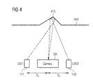
- FIG. 4 shows a schematic illustration of an imaging apparatus
- FIG. 5 shows a flowchart of a time of flight imaging method
- FIG. 6 shows a flowchart of a time of flight imaging method.
- FIG. 1 shows a schematic illustration of an imaging apparatus 100 according to an embodiment.
- the imaging apparatus 100 includes an image sensor circuit 101 including a time of flight sensor pixel 102 .
- the imaging apparatus 100 further includes a first light emitter 111 having a first spatial offset relative to the time of flight sensor pixel 102 .
- the imaging apparatus 100 further includes a second light emitter 112 having a second spatial offset relative to the time of flight sensor pixel 102 .
- the imaging apparatus 100 further includes an image processing circuit 103 configured to produce an image of a region of an object 104 based on first sensor pixel image data and second sensor pixel image data generated by the time of flight sensor pixel 102 .
- the first sensor pixel image data is based on received light emitted by the first light emitter 111 and reflected at the object's region and wherein the second sensor pixel image data is based on received light emitted by the second light emitter 112 and reflected at the object's region.
- an image of a region of an object may be produced based on first sensor pixel image data and the second sensor pixel image data. This may lead to an image of a region of the object with an improved resolution or more detailed information, for example. Furthermore, for example, multipath propagation of light transmitted from the first or second light emitter may be eliminated or reduced based on a comparison of the first and second sensor pixel image data from light emitters having different spatial offsets.
- the imaging apparatus 100 may be used to determine distance information related to an object 104 or to produce a three-dimensional image of the object 104 , for example.
- the imaging apparatus 100 may be a camera, such as a time of flight (TOF) camera.
- the object may be a person, or thing, or scenery to be photographed, for example.
- the object may be a three-dimensional (3D) scene or object, e.g. having a height, width and depth.
- the distance information related to the object may be the distance between the object or the distances between different regions of the object and at least part of the imaging apparatus, for example.
- the distance information to be determined by the apparatus 100 may be a distance between one or more different locations or one or more regions or points of the surface profile of the object and at least part of the imaging apparatus 100 , for example.
- three-dimensional information e.g. the height, width and depth
- the first 111 and second 112 light emitter may each respectively include one or more light sources, e.g. one or more light emitting diodes (LED) or lasers, for example.
- the first 111 and second 112 light emitter may each be configured to carry out active illumination of the object with a modulated optical signal, e.g. modulated infra-red light or visible light, modulated with an electrical modulation control signal, for example.
- the first 111 and the second 112 light emitter may each be configured to emit the modulated optical signal at a modulations frequency (e.g. between 1 MHz to 200 MHz) corresponding to the frequency of the modulation control signal, for example.
- a modulations frequency e.g. between 1 MHz to 200 MHz
- the first light emitter 111 may have a first spatial offset with respect to the TOF sensor pixel
- the second light emitter 112 may have a second spatial offset with respect to the TOF sensor pixel.
- the first spatial offset and the second spatial offset may be different from each other, for example.
- the first light emitter 111 and the second light emitter 112 may be arranged in different positions with respect to the imaging apparatus 100 , or with respect to the image sensor circuit 101 .
- the first light emitter 111 and the second light emitter 112 may be arranged at different equidistant positions relative to the image sensor circuit 101 (or the TOF sensor pixel).
- first light emitter 111 and the second light emitter 112 may be arranged at different non-equidistant positions relative to the time of flight sensor pixel (or the image sensor circuit 101 ). In some examples, the first light emitter and the second light emitter may be arranged symmetrically with respect to at least one axis of symmetry of the image sensor circuit 101 (or at least one axis of symmetry of the TOF sensor pixel).
- the first light emitter 111 may be configured to emit light during a first time interval and the second light emitter 112 may be configured to emit light during a second time interval.
- the first and second time interval may be different, for example.
- the first 111 and second 112 light emitter may be configured to emit light sequentially or consecutively. For example, they may be configured to emit light one after the other.
- the first light emitter 111 and the second light emitter 112 may be configured to emit differently polarized light simultaneously or sequentially.
- the image sensor circuit 101 may include a TOF sensor pixel array such as a two-dimensional array of a plurality of TOF sensor pixels.
- Each TOF sensor pixel 102 may include a photodetection circuit for the detection of light.
- the photodetection circuit may include a generation zone, e.g. a photosensitive region, such as a depletion region or space charge region, where photogenerated charge carriers (e.g. positive charge-carriers, e.g. holes, or negative charge-carriers, e.g. electrons) may be generated, for example.
- the photodetection circuit may be implemented by a photodiode, for example.
- the number of photogenerated charge carriers generated in each individual TOF sensor pixel 102 may be proportional to the intensity of light emitted from the first and/or second light emitter, subsequently reflected by the object and received by that TOF sensor pixel 102 .
- Each TOF sensor pixel 102 of the image sensor circuit 102 may produce sensor pixel image data, which may be based on an electrical signal, e.g. a voltage signal or current signal proportional to the number of photogenerated charge carriers generated by the pixel element.
- Each TOF sensor pixel may include a photonic mixing device (PMD) configured to generate the first and the second sensor pixel image data based on a respective cross-correlation measurement based on received modulated light and a reference modulation signal, for example.
- the TOF sensor pixel may be implemented as a PMD device including transparent charge collectors or photogates working in alternating bias.
- the light emitters may be configured to generate a plurality of light pulses, e.g. infra-red or visible light, at a modulation frequency of the modulation control signal.
- the reflected light pulses having the modulations frequency may be received by the image sensor circuit (e.g.
- the TOF sensor pixels which may each measure the phase delay (or phase shift) of the reflected received light with respect to modulation control signal.
- the frequency of alternating bias (push-pull signal pulses) applied to the photogates may be based on the modulation frequency of the modulation control signal which may also be used for modulation of the light emitters.
- the alternatingly biased photogates may alternatingly receive the light pulses reflected by the object. As the received light is also modulated with the same signal as the PMD image sensor circuit, the difference in the electrical signal output from the first photogate and the second photogate may be directly dependent on the phase delay between the received light and the modulation control signal and may be represented by a correlation function, for example.
- Z meas may represent amplitude information based on received light by one TOF sensor pixel.
- the amplitude information may be based on the reflectivity of the object (or the reflectivity of a region of the object from which light is reflected and received by the TOF sensor pixel), for example.
- e j ⁇ meas may represent measured phase information (indicated by ⁇ meas based on received light by the TOF sensor pixel which may include the distance information of the object.
- Each TOF sensor pixel may be configured to generate sensor pixel image data based on the cross-correlation measurement, which may be used to calculate the distance of a region of the object to the image sensor circuit 102 .
- the distance calculated may be proportional to the phase shift divided by the modulation frequency, for example.
- the distance measurement may be carried out in the time-domain by measuring the phase shift between the modulation control signal and the reflected light, for example.
- the first sensor pixel image data may be generated based on light emitted by the first light emitter 111 and received by one TOF sensor pixel, and the second sensor pixel image data may be generated based on light emitted by the second light emitter 112 and received by the TOF sensor pixel, for example.
- the image processing circuit 103 of the imaging apparatus 100 may be configured to produce an annotated depth map including an amplitude image as a depth map quality indicator, for example.
- the image processing circuit 103 may be configured to produce a 3D image of the object 104 having an increased image resolution compared to a resolution of the TOF sensor array. Furthermore, additional information from different view angles may be used for different purposes, e.g. to obtain more details from the object.
- the image processing circuit 103 may be configured to produce a three-dimensional (3D) image of the object 104 based on the first sensor pixel image data and the second sensor pixel image data generated by each TOF sensor pixel 102 of the plurality of TOF sensor pixels.
- the first sensor pixel image data may be image data generated by the TOF sensor pixel based on light emitted by the first light emitter and the second sensor pixel image data may be image data generated by the TOF sensor pixel based on light emitted by the second light emitter, for example.
- the image processing circuit 103 may be configured to produce a 3D image of the object 104 by producing a plurality of sub-image data or sub-pixel images based on the plurality of sensor pixel image data generated by one TOF sensor pixel, for example. Therefore, the 3D image of the object 104 generated by the image processing circuit 103 may be based on the generation of a plurality of sub-image data (or sub-pixel data) wherein the number of sub-image data generated is greater than the number of TOF pixels of the image sensor circuit, for example.
- the image processing circuit 103 may be configured to determine first sub-image data of a first sub-region of a region of the object (e.g. the object's region) and second sub-image data of a second sub-region of the region of the object (e.g. the object's region).
- the first sub-region and the second sub-region may be different sub-regions of the region of the object.
- the number of sub-regions, s corresponds to a number of light emitters, r, having the different spatial offsets, for example.
- the image processing circuit 103 may determine, based on a number of sensor pixel image data of a region of the object generated by one TOF sensor pixel, a number of sensor pixel sub-image data each corresponding to a respective different sub-region of the region of the object and corresponding to the number of light emitters, r, having different spatial offsets whose emitted light was used to generate the number of sensor pixel image data of the region of the object.
- the number of sensor pixel sub-image data d may correspond to (or be equal to) the number of light emitters used to emit light and may contain or include information related to the region of the object.
- the number of sensor pixel sub-image data, d may also correspond to (or be equal to) the number of number of sub-regions, s, of the object for which sensor pixel sub-image data is generated.
- the image processing circuit 103 may be configured to determine the first and the second sub-image data based on the first and the second sensor pixel image data. By subsequently or sequentially activating different illumination units (or e.g. light emitters at different positions), the resolution of a TOF system may be increased, e.g. the resolution of a 3D image produced by the imaging apparatus 100 or a TOF system may be increased.
- the image processing circuit 103 may additionally or alternatively be configured to produce a reduced-error image of the object based on a comparison of phase information of the first sensor pixel image data and the second sensor pixel image data.
- the image processing circuit may be configured to produce the image of the object's region based on a selection of one of the first sensor pixel image data and the second sensor pixel image data having a minimum phase value.
- sensor pixel image data generated by light emitters having different spatial offsets may be used to reduce multipath propagation based on the different positions of the light emitters. Images which suffer from high multipath propagation may be eliminated, or reduced, and a produced 3D image may be based on image data with minimal or reduced multipath propagation, for example.
- FIGS. 2A to 2D show a schematic illustration of an imaging apparatus 200 according to an embodiment.
- the imaging apparatus 200 includes an image sensor circuit including a plurality of time of flight sensor pixels.
- the imaging apparatus 200 further includes a first light emitter 111 having a first spatial offset relative to the image sensor circuit 101 .
- the imaging apparatus 200 further includes a second light emitter 112 having a second spatial offset relative to the image sensor circuit 101 .
- the imaging apparatus 200 further includes an image processing circuit 103 configured to produce an image of a region of an object based on first sensor pixel image data and second sensor pixel image data generated by a time of flight sensor pixel of the plurality of time of flight sensor pixels.
- the image includes first sub-image data of a first sub-region of the object and second sub-image data about a second sub-region of the object.
- the first sensor pixel image data is based on received light emitted by the first light emitter and reflected by the object and wherein the second sensor pixel image data is based on received light emitted by the second light emitter and reflected by the object.
- an image of a region of an object may be produced based on first sensor pixel image data and the second sensor pixel image data.
- the image of the region of the object may have an improved resolution or more detailed information, for example.
- the imaging apparatus 200 may be similar to the imaging apparatus described with respect to FIG. 1 , for example.
- the imaging apparatus 200 may be configured to produce a three-dimensional (3D) image having increased resolution or with increased detail, for example.
- the imaging apparatus 200 may be a TOF system, which may measure amplitude and phase (vectors), for example.
- Measured phase information may be indicative of distance information of the object (e.g. a distance from a light emitter to the object and from the object to a reference, such as to the imaging apparatus or to the imaging sensor circuit), for example.
- the measured amplitude information may be indicative of the reflectivity of the object, for example.
- unknown parameters For generating sensor pixel sub-image data information based on sensor pixel image data information, unknown parameters may be generated. For example, for splitting up one pixel into four sub-pixels, 8 unknown parameters (e.g. four amplitudes and four phases) may be calculated, for example.
- FIG. 2A shows an example of sensor pixel image data being measured by the imaging apparatus 200 .
- Light may be emitted by one light emitter (e.g. the first light emitter) during a first time interval.
- the measured sensor pixel image data by one TOF sensor pixel which may be based on light emitted by the light emitter and received by the TOF sensor pixel, may be represented by the vector Z meas , which may be a superposition of a number of sub-image data (or sub-pixels) reflected from different sub-regions (e.g. sub-regions A, B, C and D) of a region of the object.
- the superposition of the sub-image data is shown by the arrows emitted by the first light emitter 111 and reflected from the different sub-regions and received by the plurality of TOF sensor pixels, for example.
- FIG. 2B shows that the measured vector Z meas or Z measured may be a superposition (or addition) of four sub-pixels (or e.g. four sub-image data).
- Z meas Z A +Z B +Z C +Z D .
- a number of equations may be obtained from measurements by the plurality of light emitters (e.g. LEDs 1 , 2 , 3 and 4 ) having different spatial offsets.
- a different measured vector may be obtained based on received light from different light emitters at different positions.
- a number of equations may be obtained based on sensor pixel image data generated by different light emitters having different spatial offsets.
- eight equations may be obtained from four different measurements with different LED positions (for different distances and/or phase).
- FIG. 2C shows a front view of the imaging apparatus 200 according to an embodiment.
- the imaging apparatus 200 may include a plurality of light emitters e.g. four light emitters (e.g. a first, second, third and fourth light emitter), or e.g. four LEDs which may each be arranged at different equidistant positions relative to the image sensor circuit 101 or relative to the 2D sensor pixel array.
- the plurality of light emitters may be arranged symmetrically with respect to an axis of symmetry (e.g. a horizontal or vertical or diagonal line of symmetry) of the image sensor circuit 101 or of the array of TOF sensor pixels.
- the plurality of light emitters may each be arranged coplanar to a planar surface of the 2D sensor pixel array.
- the planar surface of the 2D sensor pixel array may be the surface area of the sensor pixel array receiving for receiving reflected light from the light emitters, for example.
- the distance, x 1 , between a light emitter of the plurality of light emitters and the image sensor circuit 101 may be greater than 1 cm, e.g. greater than 5 cm, or e.g. greater than 10 cm. In other examples, the distances between each of the plurality of light emitters and the image sensor circuit 101 may be different, for example. In some examples, the distance between a light emitter and a neighboring light emitter may be greater than 2 cm, e.g. greater than 5 cm, or e.g. greater than 10 cm.
- a light emitter control circuit may control the emission of light from the plurality of light emitters, for example.
- the light emitter control circuit may be configured to trigger the light emitters to emit light consecutively or sequentially at a modulations frequency of a modulation control signal.
- the light emitter control circuit may be configured to trigger the first light emitter followed by the second light emitter, followed by the third light emitter and following by the fourth light emitter.
- the image sensor circuit 101 (or each TOF sensor pixel) may be configured to receive light emitted by the first light emitter and reflected by the object during a first time interval.
- the image sensor circuit 101 (or each TOF sensor pixel) may be configured to receive light emitted by the second light emitter and reflected by the object during a second time interval.
- the image sensor circuit 101 (or each TOF sensor pixel) may be configured to receive light emitted by the third light emitter and reflected by the object during a third time interval.
- the image sensor circuit 101 (or each TOF sensor pixel) may be configured to receive light emitted by the fourth light emitter and reflected by the object during a fourth time interval, for example.
- the first to fourth time interval may be consecutive time intervals, for example.
- the first and second light emitter may be part of a single light emitting source (e.g. a single LED or a single group of LEDs).
- the light emitter control circuit may be configured to selectively control the emission of light by the single light emitting source at different exit points, where the exit points may have different spatial offsets with respect to the image sensor circuit.
- the exit points of the first light emitter and the second light emitter may be controlled by the control circuit via an optical switching board, for example.
- the first light emitter and the second light emitter may each respectively include a light emitting portion of a light transmitter or may include light emitting optical or glass fibers controlled by optical switches.
- the light emitter control circuit may further control the emission of light from the plurality of light emitters, so that in a first light emission mode, a single light emitter may be configured to emit light at the modulations frequency and the image produced by the image processing circuit may be based on light emitted by that single light emitter and received by the image sensing circuit, for example. For example, this may be when the imaging apparatus enters a low power mode and when the low power mode is detected by the light emitter control circuit, for example.
- the first light emission mode may be used for example, in the low power mode where the entire (increased) pixel resolution (e.g. the increased image resolution with more detailed information) is not necessarily needed, for example.
- a plurality of light emitters e.g.
- the low power mode may be detected by the TOF camera (e.g. the imaging apparatus) itself, for example, by gesture recognition, or e.g. by detecting that no hand is present or that the hand is at rest.
- the TOF camera may self-recognize that increased resolution is not needed, and the imaging apparatus can enter the low power mode (e.g. the first light emission mode).
- the imaging apparatus can enter the low power mode (e.g. the first light emission mode).
- only one LED may be activated.
- the light may be directed to only one light emission exit point.
- the light emitter control circuit may be configured to trigger the light emitters to emit differently polarized light simultaneously or sequentially.
- FIG. 2D shows that the measured (e.g. measured vector Z meas _ LED1 by one TOF sensor pixel based on light emitted by the first light emitter and received by the TOF sensor pixel may be a superposition (or addition) of four sub-pixels (or e.g. four sub-image data).
- Z measured _ LED1 Z A +Z B +Z C +Z D .
- Z A , Z B , Z C and Z D may each include respective phase information ⁇ A _ LED1 , ⁇ B _ LED1 , ⁇ C _ LED1 and ⁇ D _ LED1 for each of the respective sub-image data corresponding to sub-regions A, B, C and D, for example.
- the phase information ⁇ A _ LED1 , ⁇ B _ LED1 , ⁇ C _ LED1 and ⁇ D _ LED1 may each represent a phase offset with respect to a reference phase value, for example.
- four sub-image data may be obtained.
- an example is shown herein which describes how two sub-image data may be determined based on the measured sensor pixel image data using two different light emitters at different positions, for example.
- the measurement may be the superposition of sub-pixels (or sub-image data) e.g. a superposition of the first sub-image data and second sub-image data.
- Z meas
- two measurements with two subsequently (or sequentially) activated light emitters may be represented by the equations:
- Z meas1
- Z meas2
- Z m may represent measured sensor pixel image data, e.g. first and second measured sensor pixel image data represented by Z meas1 and Z meas2 respectively.
- Z meas1 and Z meas2 may include intensity and phase information related to the first and second sensor pixel image data respectively.
- the sub-image data to be determined may be represented by the vector Z wanted , which may represent first and second sub-image (or sub-pixel) data, for example.
- a set of time of flight offset values may be determined by the image processing circuit 103 , for example.
- the set of time of flight offsets ⁇ delay may include a plurality of time of flight values, e.g. 2 r time of flight offsets, where r represents the number of light emitters having different spatial offsets, or the number of measurements carried out based on the different light emitters.
- r represents the number of light emitters having different spatial offsets, or the number of measurements carried out based on the different light emitters.
- r 2
- ⁇ delay [ e j ⁇ ⁇ ⁇ ⁇ ⁇ ⁇ ⁇ a ⁇ ⁇ 1 e j ⁇ ⁇ ⁇ ⁇ ⁇ ⁇ b ⁇ ⁇ 1 e j ⁇ ⁇ ⁇ ⁇ ⁇ ⁇ a ⁇ ⁇ 2 e j ⁇ ⁇ ⁇ ⁇ ⁇ ⁇ b ⁇ ⁇ 2 ] ,
- e j ⁇ a1 , e j ⁇ b1 , e j ⁇ a2 , and e j ⁇ b2 are indicative of the first, second, third, and fourth time of flight offset values, respectively.
- Z m ⁇ delay ⁇ Z wanted ,
- the image processing circuit may be configured to determine the first and the second sub-image data based on the equation:
- Z a and Z b may each include intensity and phase information related to the first and second sub-image data respectively, for example.
- the image processing circuit 103 may be configured to obtain phase-shifted versions of the first and the second sensor pixel image data based on a combination of the first and the second sensor pixel image data with the set of time of flight offsets ⁇ delay .
- the image processing circuit 103 may be configured to produce the first sub-image data (e.g. Z a ) and the second sub-image data (e.g. Z b ) based on a linear combination of phase-shifted versions of the first and the second sensor pixel image data.
- the image processing circuit 103 may be configured to determine the first sub-image data Z a based on a first linear combination of phase-shifted versions of the first and the second sensor pixel image data.
- the image processing circuit 103 may be configured to determine the second sub-image data Z b based on at least a second linear combination of phase-shifted versions of the first and the second sensor pixel image data. For example,
- FIGS. 2A to 2D may comprise one or more optional additional features corresponding to one or more aspects mentioned in connection with the proposed concept or one or more embodiments described above (e.g. FIG. 1 ) or below (e.g. FIGS. 3 to 5 ).
- FIG. 3 shows an example of the imaging apparatus (e.g. imaging apparatus 200 ) and geometrical values used by the image processing circuit for producing an improved 3D image, according to an embodiment.
- the image processing circuit 103 may be configured to determine the time-of flight offsets.
- the image processing circuit may be configured to carry out a factor correction process to derive the time of flight offset values by multiplying each offset by a factor 2 ⁇ f/c, for example.
- the set of time of flight offset values may be derived by the image processing circuit 103 based on the following equations:
- the first time of flight offset ⁇ a1 may denote an offset (e.g. a phase offset or phase difference) between a reference time of flight ⁇ a0 of received light emitted by a reference light emitter and reflected at the object's first sub-region (e.g. region A) and a time of flight of received light ⁇ a1 emitted by the first light emitter 111 and reflected at the object's first sub-region.
- the first time of flight offset ⁇ a1 may be based on the first spatial offset, for example.
- the second time of flight offset ⁇ b1 may denote an offset (e.g. a phase offset or phase difference) between a reference time of flight ⁇ b0 of received light emitted by the reference light emitter and reflected at the object's second sub-region (e.g. region B) and a time of flight of received light ⁇ b1 emitted by the first light emitter 111 and reflected at the object's second sub-region.
- the second time of flight offset ⁇ b1 may be based on the first spatial offset, for example.
- the third time of flight offset ⁇ a2 may denote an offset (e.g. a phase offset or phase difference) between the reference time of flight ⁇ a0 of received light emitted by the reference light emitter and reflected at the object's first sub-region (e.g. region A) and a time of flight of received light ⁇ a2 emitted by the second light emitter 112 and reflected at the object's first sub-region.
- the third time of flight offset ⁇ a2 may be based on the second spatial offset, for example.
- the fourth time of flight offset ⁇ b2 may denote an offset (e.g. a phase offset or phase difference) between the reference time of flight ⁇ b0 of received light emitted by the reference light emitter and reflected at the object's second sub-region (e.g. region B) and a time of flight of received light ⁇ b2 emitted by the second light emitter 112 and reflected at the object's second sub-region.
- the fourth time of flight offset ⁇ b2 may be based on the second spatial offset, for example.
- ⁇ a1 and ⁇ b1 may be the time of flight offsets related to the first light emitter (e.g. LED 1 ) and ⁇ a2 and ⁇ b2 may be the time of flight offsets related to the second light emitter (e.g. LED 2 ).
- the reference time of flight values may be obtained, for example by carrying out a reference TOF measurement.
- all light emitters may emit light simultaneously.
- the light emitter control circuit may be configured to trigger the first and second light emitter to simultaneously emit light.
- the light reflected by the object may be received by the TOF sensor pixel, and reference sensor pixel image data including amplitude and phase information about the received light, may be generated by the TOF sensor pixel.
- the first reference sub-image data ⁇ a0 and second reference sub-image data ⁇ b0 may be determined based on the reference sensor pixel image data generated by the image processing circuit 103 based on the reference cross-correlation measurement, for example.
- the reference TOF measurement may be carried out before the sequential emission of each individual light emitter at the different positions with respect to the image sensor circuit, for example.
- the reference TOF measurement may be based on the emission of light from only one light emitter, or any combination of light emitters for example.
- the first reference sub-image data ⁇ a0 and the second reference sub-image data ⁇ b0 may each be generated or determined based on a first and second sub-image position offset, respectively.
- the imaging apparatus 200 may include a collector optic having a known angle range (e.g. a 90° angle range) for collecting or receiving light reflected by the object.
- the first reference sub-image data ⁇ a0 may be determined based on a time of flight sensor pixel position offset, a first sub-image position offset, and a distance between a region of the object and the TOF sensor pixel array, for example.
- the second reference sub-image data ⁇ b0 may be determined based on the time of flight sensor pixel position offset, a second sub-image position offset, and a distance between a region of the object and the TOF sensor pixel array, for example.
- the first reference sub-image data ⁇ a0 and the second reference sub-image data ⁇ b0 may each be denoted by
- x z 2 ⁇ R x represents a SLID-image position offset
- x z represents a distance between a region of the object and the TOF sensor pixel array.
- x x may be a time of flight sensor pixel position offset, which may be determined based on the geometry of the imaging apparatus and a position of the TOF sensor pixel in the TOF sensor pixel array, for example.
- x z may be a perpendicular distance between a region of the object and a planar surface of the TOF sensor pixel array, or a shortest distance between a region of the object and a virtual plane coplanar with the planar surface of the TOF sensor pixel array.
- the value x z may be derived from the reference measurement, for example.
- R x may be an absolute value of a first or second sub-image position offset, based on a pixel size of an image of a region of the object being based
- the first (reference) sub-image data may have a negative spatial offset with respect to a line of reference in the TOF sensor pixel and the second (reference) sub-image data may have a positive spatial offset with respect to the line of reference.
- the line of reference may be an axis of symmetry (e.g. a vertical or horizontal axis of symmetry) of the TOF sensor pixel, for example.
- x 1 may be an absolute value of a spatial offset of the first and second light emitter.
- the first spatial offset may be a negative spatial offset with respect to a line of reference 314 (or e.g. an axis of symmetry) of the image sensor circuit 103 or the imaging apparatus 100 and the second spatial offset may be a positive spatial offset with respect to the line of reference (or e.g. an axis of symmetry).
- the first time of flight offset ⁇ a1 may be associated with the first light emitter and the first sub-region.
- the second time of flight offset ⁇ b1 may be associated with the first light emitter and the second sub-region.
- the third time of flight offset ⁇ a2 may be associated with the second light emitter and the first sub-region.
- the fourth time of flight offset ⁇ b2 may be associated with the second light emitter and the second sub-region.
- the first to fourth time of flight offsets may each be derived based on a phase offset between a reference time of flight of received light emitted by a reference light emitter and reflected at a sub-region of the object and a time of flight of received light emitted respectively by the first to fourth light emitters and reflected at the sub-region of the object.
- the set of time of flight offset values derived by the image processing circuit 103 may be further based on a factor related to the speed of light c and the modulation frequency f.
- the image processing circuit may be configured to carry out a factor correction process to derive the time of flight offset values by multiplying each offset by a factor
- the first sub-image data (e.g. Z a ) and the second sub-image data (e.g. Z b ) for one TOF sensor pixel may be determined based on a linear combination of the time of flight offset values and the measured first and second sensor pixel image data by that TOF sensor pixel, for example.
- the image processing circuit may be configured to determine first sub-image data and second sub-image data for every TOF sensor pixel of the plurality of TOF sensor pixels, for example.
- a measurement of the sensor pixel image data may be (or include) the superposition of sub-pixels of sub-image data (e.g. four sub-pixels).
- Z meas
- Z meas1
- Z meas1
- Z meas2
- Z meas3
- Z meas1 Z a ⁇ e j ⁇ a1 + Z b ⁇ e j ⁇ b1 + Z c ⁇ e j ⁇ c1 + Z d ⁇ e j ⁇ d1
- Z meas2 Z a ⁇ e j ⁇ a2 + Z b ⁇ e j ⁇ b2 + Z c ⁇ e j ⁇ c2 + Z d ⁇ e j ⁇ d2
- Z meas3 Z a ⁇ e j ⁇ a3 + Z b ⁇ e j ⁇ b3 + Z c ⁇ e j ⁇ c3 + Z d ⁇ e j ⁇ d3
- Z meas4 Z a ⁇ e j ⁇ a4 + Z b ⁇ e j ⁇ b4 + Z c ⁇ e j ⁇ c4 + Z d ⁇ e j ⁇ d4
- Z m may represent measured sensor pixel image data, e.g. first to fourth sensor pixel image data represented by Z meas1 , Z meas2 , Z meas3 and Z meas4 respectively.
- Z m _ [ Z meas ⁇ ⁇ 1 _ Z meas ⁇ ⁇ 1 _ Z meas ⁇ ⁇ 3 _ Z meas ⁇ ⁇ 4 _ ]
- Each of the sub-image data to be determined may be represented by the vector Z wanted , which may represent first to fourth sub-image (or sub-pixel) data, for example.
- a set of time of flight values may be determined by the image processing circuit 103 , for example.
- the set of time of flight values ⁇ delay may include a plurality of time of flight values, e.g. 2 m number of delay values e.g. 16 delay values, for example.
- ⁇ delay [ e j ⁇ ⁇ ⁇ ⁇ ⁇ ⁇ ⁇ a ⁇ ⁇ 1 e j ⁇ ⁇ ⁇ ⁇ ⁇ b ⁇ ⁇ 1 e j ⁇ ⁇ ⁇ ⁇ ⁇ ⁇ c ⁇ ⁇ 1 e j ⁇ ⁇ ⁇ ⁇ ⁇ ⁇ d ⁇ ⁇ 1 e j ⁇ ⁇ ⁇ ⁇ ⁇ ⁇ a ⁇ ⁇ 2 e j ⁇ ⁇ ⁇ ⁇ ⁇ ⁇ b ⁇ ⁇ 2 e j ⁇ ⁇ ⁇ ⁇ ⁇ c ⁇ ⁇ 2 e j ⁇ ⁇ ⁇ ⁇ ⁇ ⁇ d ⁇ ⁇ 2 e j ⁇ ⁇ ⁇ ⁇ ⁇ ⁇ a ⁇ ⁇ 3 e j ⁇ ⁇ ⁇ ⁇ ⁇ ⁇ ⁇ ⁇ b ⁇ ⁇ 3 e j ⁇ ⁇ ⁇ ⁇ ⁇ ⁇ ⁇
- the image processing circuit 103 may be configured to produce the different sub-image data (e.g. Z a , Z b , Z c and Z d ) based on a linear combination of phase-shifted versions of the first, second, third and fourth sensor pixel image data.
- the different sub-image data e.g. Z a , Z b , Z c and Z d
- FIG. 3 may comprise one or more optional additional features corresponding to one or more aspects mentioned in connection with the proposed concept or one or more embodiments described above (e.g. FIGS. 1 to 2D ) or below (e.g. FIGS. 4 to 5 ).
- FIG. 4 shows a schematic illustration of an imaging apparatus 400 according to an embodiment.
- the imaging apparatus 400 may be similar to the imaging apparatus described with respect to FIGS. 1 to 3 , for example.
- the image processing circuit 403 may be configured to produce a reduced-error image of the object based on a comparison of phase information of the first sensor pixel image data and the second sensor pixel image data. For example, for a TOF system, it may be very challenging to measure corners 415 of an object 404 .
- the image processing circuit 403 may be configured to produce the image of the object's region based on a selection of one of the first sensor pixel image data and the second sensor pixel image data having a minimum phase value, for example. In this way, the light emitters having different spatial offsets may be used to compare multipath propagation caused by the different positions of the light emitters.
- Images which suffer from high multipath propagation may be eliminated, or reduced, and a produced 3D image may be based on image data with minimal or reduced multipath propagation, for example.
- pixel image data having a minimum phase value may be indicative of a minimal amount of multipath propagation in a TOF system
- the sensor pixel image data having the minimum (or smallest) measured phase value may be selected. In this way, multipath propagation in a TOF system may be reduced or eliminated, for example.
- FIG. 4 may comprise one or more optional additional features corresponding to one or more aspects mentioned in connection with the proposed concept or one or more embodiments described above (e.g. FIGS. 1 to 3 ) or below (e.g. FIG. 5 ).
- FIG. 5 shows a flow chart of a time of flight imaging method 500 according to an embodiment.
- the method 500 includes receiving 510 , by a time of flight sensor pixel, light emitted by a first light emitter having a first spatial offset relative to the time of flight sensor pixel and reflected by a region of an object to generate first sensor pixel image data.
- the method 500 further includes receiving 520 , by the time of flight sensor pixel, light emitted by a second light emitter having a second spatial offset relative to the time of flight sensor pixel and reflected by the region of the object to generate second sensor pixel image data.
- the method 500 further includes producing 530 an image of the object's region based on the first and second sensor pixel image data generated by the time of flight sensor pixel.
- Producing the image may include determining a first sub-image data of a first sub-region of the object's region and second sub-image data of a (different) second sub-region of the object's region.
- the number of sub-regions may correspond to a number of light emitters having different spatial offsets
- the first and the second image sub-image data may be determined based on the first and the second sensor pixel image data.
- the method may further include determining the first sub-image based on a first linear combination of phase-shifted versions of the first and the second sensor pixel image data.
- the method may further include determining the second sub-image based on a second linear combination of phase-shifted versions of the first and the second sensor pixel image data.
- the phase-shifted versions of the first and the second sensor pixel image data may be obtained based on a combination of the first and the second sensor pixel image data with a set of time of flight offsets.
- a first time of flight offset may be associated with the first light emitter and the first sub-region.
- a second time of flight offset may be associated with the first light emitter and the second sub-region.
- a third time of flight offset of the set may be associated with the second light emitter and the first sub-region.
- a fourth time of flight offset may be associated with the second light emitter and the second sub-region.
- the method may further include determining a first reference sub-image and a second reference sub-image based on a reference TOF measurement.
- the reference TOF measurement may be carried out by receiving light emitted by at least one light emitter and reflected by the object.
- FIG. 5 may comprise one or more optional additional features corresponding to one or more aspects mentioned in connection with the proposed concept or one or more embodiments described above (e.g. FIGS. 1 to 4 ) or below (e.g. FIG. 6 ).
- FIG. 6 shows a flow chart of a time of flight imaging method 600 according to an embodiment.
- the method 600 includes receiving 610 , by a time of flight sensor pixel, light emitted by a first light emitter having a first spatial offset relative to the time of flight sensor pixel and reflected by a region of an object to generate first sensor pixel image data.
- the method 600 further includes receiving 620 , by the time of flight sensor pixel, light emitted by a second light emitter having a second spatial offset relative to the time of flight sensor pixel and reflected by the region of the object to generate second sensor pixel image data.
- the method 600 further includes producing an image of the region of the object based on a selection of one of the first and second sensor pixel image data.
- the selection may be based on a comparison of phase information of the first and second sensor pixel image data, for example.
- Various embodiments relate to increasing the resolution of a time of flight (TOF) system.
- Various embodiments may include sensor shifting principles, stereoscopy principles and Radar principles with multiple transmit and receive antennas, for example.
- Example embodiments may further provide a computer program having a program code for performing one of the above methods, when the computer program is executed on a computer or processor.
- a person of skill in the art would readily recognize that acts of various above-described methods may be performed by programmed computers.
- some example embodiments are also intended to cover program storage devices, e.g., digital data storage media, which are machine or computer readable and encode machine-executable or computer-executable programs of instructions, wherein the instructions perform some or all of the acts of the above-described methods.
- the program storage devices may be, e.g., digital memories, magnetic storage media such as magnetic disks and magnetic tapes, hard drives, or optically readable digital data storage media.
- Functional blocks denoted as “means for . . . ” shall be understood as functional blocks comprising circuitry that is configured to perform a certain function, respectively.
- a “means for s.th.” may as well be understood as a “means configured to or suited for s.th.”.
- a means configured to perform a certain function does, hence, not imply that such means necessarily is performing the function (at a given time instant).
- any functional blocks labeled as “means”, “means for providing a sensor signal”, “means for generating a transmit signal.”, etc. may be provided through the use of dedicated hardware, such as “a signal provider”, “a signal processing unit”, “a processor”, “a controller”, etc. as well as hardware capable of executing software in association with appropriate software.
- any entity described herein as “means”, may correspond to or be implemented as “one or more modules”, “one or more devices”, “one or more units”, etc.
- the functions may be provided by a single dedicated processor, by a single shared processor, or by a plurality of individual processors, some of which may be shared.
- processor or “controller” should not be construed to refer exclusively to hardware capable of executing software, and may implicitly include, without limitation, digital signal processor (DSP) hardware, network processor, application specific integrated circuit (ASIC), field programmable gate array (FPGA), read only memory (ROM) for storing software, random access memory (RAM), and non-volatile storage.
- DSP digital signal processor
- ASIC application specific integrated circuit
- FPGA field programmable gate array
- ROM read only memory
- RAM random access memory
- non-volatile storage non-volatile storage.
- Other hardware conventional and/or custom, may also be included.
- each claim may stand on its own as a separate embodiment. While each claim may stand on its own as a separate embodiment, it is to be noted that—although a dependent claim may refer in the claims to a specific combination with one or more other claims—other embodiments may also include a combination of the dependent claim with the subject matter of each other dependent or independent claim. Such combinations are proposed herein unless it is stated that a specific combination is not intended. Furthermore, it is intended to include also features of a claim to any other independent claim even if this claim is not directly made dependent to the independent claim.
- a single act may include or may be broken into multiple sub acts. Such sub acts may be included and part of the disclosure of this single act unless explicitly excluded.
Landscapes
- Engineering & Computer Science (AREA)
- Physics & Mathematics (AREA)
- General Physics & Mathematics (AREA)
- Computer Networks & Wireless Communication (AREA)
- Radar, Positioning & Navigation (AREA)
- Remote Sensing (AREA)
- Electromagnetism (AREA)
- Multimedia (AREA)
- Signal Processing (AREA)
- Optical Radar Systems And Details Thereof (AREA)
- Length Measuring Devices By Optical Means (AREA)
- Computer Graphics (AREA)
- Theoretical Computer Science (AREA)
Abstract
Description
Z meas =|Z meas |·e jφ
may represent the sensor pixel image data measured by the TOF sensor pixel by the correlation measurement, for example.
Z meas =|Z meas |·e jφ
Z meas =|Z a |·e jφ
Z meas1 =|Z a |·e jφ
Z meas2 =|Z a |·e jφ
Z meas1 = Z a ·e jΔφ
Z meas2 = Z a ·e jΔφ
where xx represents the time of flight sensor pixel position offset,
represents a SLID-image position offset, and xz represents a distance between a region of the object and the TOF sensor pixel array.
may be an absolute value of a first or second sub-image position offset, based on a pixel size of an image of a region of the object being based
on the geometry of the imaging apparatus and receiving angle of the collector optic. For example, the first (reference) sub-image data may have a negative spatial offset with respect to a line of reference in the TOF sensor pixel and the second (reference) sub-image data may have a positive spatial offset with respect to the line of reference. The line of reference may be an axis of symmetry (e.g. a vertical or horizontal axis of symmetry) of the TOF sensor pixel, for example.
for example.
Z meas =|Z a |·e jφ
Z meas1 =|Z a |·e j(φ
Z meas1 =|Z a |·e jφ
Z meas2 =|Z a |·e jφ
Z meas3 =|Z a |·e jφ
Z meas4 =|Z a |·e jφ
Z meas1 = Z a ·e jΔφ
Z meas2 = Z a ·e jΔφ
Z meas3 = Z a ·e jΔφ
Z meas4 = Z a ·e jΔφ
Claims (20)
Applications Claiming Priority (3)
| Application Number | Priority Date | Filing Date | Title |
|---|---|---|---|
| DE102014115310 | 2014-10-21 | ||
| DE102014115310.3 | 2014-10-21 | ||
| DE102014115310.3A DE102014115310A1 (en) | 2014-10-21 | 2014-10-21 | Image forming apparatus and a runtime image forming method |
Publications (2)
| Publication Number | Publication Date |
|---|---|
| US20160112696A1 US20160112696A1 (en) | 2016-04-21 |
| US10091492B2 true US10091492B2 (en) | 2018-10-02 |
Family
ID=55637759
Family Applications (1)
| Application Number | Title | Priority Date | Filing Date |
|---|---|---|---|
| US14/887,400 Active 2036-11-23 US10091492B2 (en) | 2014-10-21 | 2015-10-20 | Imaging apparatuses and a time of flight imaging method |
Country Status (3)
| Country | Link |
|---|---|
| US (1) | US10091492B2 (en) |
| CN (1) | CN105554418B (en) |
| DE (1) | DE102014115310A1 (en) |
Cited By (2)
| Publication number | Priority date | Publication date | Assignee | Title |
|---|---|---|---|---|
| US10726574B2 (en) * | 2017-04-11 | 2020-07-28 | Dolby Laboratories Licensing Corporation | Passive multi-wearable-devices tracking |
| US20240134036A1 (en) * | 2022-10-12 | 2024-04-25 | Electronics And Telecommunications Research Institute | Image generating device setting virtual transmitters and receivers, and method of operating the same |
Families Citing this family (20)
| Publication number | Priority date | Publication date | Assignee | Title |
|---|---|---|---|---|
| US10225567B2 (en) * | 2013-10-08 | 2019-03-05 | Sharp Kabushiki Kaisha | Image decoder, image encoder, and encoded data converter |
| EP3193190B1 (en) * | 2016-01-15 | 2023-04-12 | Sony Depthsensing Solutions N.V. | A detector device with majority current and a circuitry for controlling the current |
| CN108572369A (en) * | 2017-03-13 | 2018-09-25 | 北醒(北京)光子科技有限公司 | A kind of micro mirror scanning probe device and detection method |
| CN110431441B (en) * | 2017-03-19 | 2023-09-15 | 科维塔公司 | System and method for modulated image capture |
| EP3654633A4 (en) * | 2017-07-12 | 2020-05-27 | Sony Corporation | IMAGING DEVICE AND IMAGE GENERATION METHOD |
| EP3521751A1 (en) * | 2018-02-01 | 2019-08-07 | Primetals Technologies Austria GmbH | Device and method for identification of equipment in metallurgical industrial installations |
| US10630384B2 (en) * | 2018-06-13 | 2020-04-21 | Infineon Technologies Ag | Dual-mode optical devices for time-of-flight sensing and information transfer, and apparatus, systems, and methods utilizing same |
| US10340116B1 (en) * | 2018-06-13 | 2019-07-02 | Applied Materials Israel Ltd. | Imaging an area that includes an upper surface and a hole |
| US11994627B2 (en) * | 2019-07-12 | 2024-05-28 | Artis, Llc | Microsecond time of flight (μTOF) sensor |
| EP3767330B1 (en) * | 2019-07-18 | 2023-06-21 | Infineon Technologies AG | Method and apparatus for determining relative motion between a time-of-flight camera and an object in a scene sensed by the time-of-flight camera |
| DE102019121340A1 (en) * | 2019-08-07 | 2021-02-11 | Infineon Technologies Ag | METHOD AND DEVICE FOR DETERMINING MALFUNCTION AND SENSOR SYSTEM |
| CN112824934B (en) * | 2019-11-20 | 2024-05-07 | 深圳市光鉴科技有限公司 | TOF multipath interference removal method, system, equipment and medium based on modulated light field |
| CN111103593B (en) * | 2019-12-31 | 2025-05-16 | 深圳市欢创科技股份有限公司 | Distance measurement module, robot, distance measurement method and non-volatile readable storage medium |
| JP2021117036A (en) * | 2020-01-23 | 2021-08-10 | 株式会社日立エルジーデータストレージ | Measurement value correction method of range-finding device |
| CN113542712B (en) * | 2020-04-16 | 2024-08-20 | 钰立微电子股份有限公司 | Multi-depth information processing method and processing system |
| US11428792B2 (en) * | 2020-06-08 | 2022-08-30 | Stmicroelectronics (Research & Development) Limited | Routing for DTOF sensors |
| DE102020120542A1 (en) * | 2020-08-04 | 2022-02-10 | Valeo Schalter Und Sensoren Gmbh | Generation of a measurement data set using an active sensor system |
| EP3964857A1 (en) * | 2020-09-07 | 2022-03-09 | Infineon Technologies AG | Method and apparatus for determining a reflectivity value indicating a reflectivity of an object |
| TWI746313B (en) * | 2020-12-15 | 2021-11-11 | 和碩聯合科技股份有限公司 | Method and system for distance detection |
| FR3132959B1 (en) * | 2022-02-22 | 2024-06-28 | St Microelectronics Grenoble 2 | Time of flight sensor |
Citations (12)
| Publication number | Priority date | Publication date | Assignee | Title |
|---|---|---|---|---|
| DE4011041A1 (en) | 1989-04-08 | 1991-10-10 | Christian Wasserthal | Detecting bodies in path of motor vehicle - illuminating data by two differentially coloured sources or with polarised light and evaluating received light |
| US6122042A (en) | 1997-02-07 | 2000-09-19 | Wunderman; Irwin | Devices and methods for optically identifying characteristics of material objects |
| DE10342800A1 (en) | 2003-09-16 | 2005-04-28 | Fraunhofer Ges Forschung | Apparatus for absorbing and / or emitting radiation, method for producing such apparatus and method for analyzing fluids |
| DE102004032489A1 (en) | 2004-07-05 | 2006-01-26 | Fraunhofer-Gesellschaft zur Förderung der angewandten Forschung e.V. | Microstructurized device, used as sensor or actor, e.g. metal oxide gas sensor, infrared radiator, flow sensor, pyrometer or other thermopile-based microsensor, has thermal decoupling polymer between thermally active zone and support |
| DE102004032176A1 (en) | 2004-07-02 | 2006-01-26 | Robert Bosch Gmbh | Coated micromechanical radiator |
| DE102006044794A1 (en) | 2006-09-14 | 2008-03-27 | Schefenacker Vision Systems Germany Gmbh | Vehicle-based light detection and ranging system for use in vehicle light i.e. rear light, has transmission unit that is integrated into vehicle light, where transmission unit has LEDs that are used as transmitters |
| WO2010012697A1 (en) | 2008-07-28 | 2010-02-04 | Lion Systems S.A. | Method and device for enhancing the resolution of a camera |
| US20100258708A1 (en) * | 2007-12-06 | 2010-10-14 | U.S. Government As Represented By The Secretary Of The Army | Method and system for lidar using quantum properties |
| DE102012205448A1 (en) | 2011-04-06 | 2012-10-11 | GM Global Technology Operations LLC (n.d. Ges. d. Staates Delaware) | Method and apparatus for an object detection system using two modulated light sources |
| CN103439295A (en) | 2013-08-16 | 2013-12-11 | 中国科学院上海光学精密机械研究所 | Full-depth frequency-domain Doppler optical coherence tomography method |
| DE102013002683A1 (en) | 2013-02-15 | 2014-08-21 | Volkswagen Aktiengesellschaft | Method for vehicle for determining distance information and for transferring of transmission data, involves generating modulated signal depending on transmission data to be transmitted from vehicle |
| US20140293262A1 (en) * | 2013-03-27 | 2014-10-02 | The Boeing Company | Imaging System for Wire Detection |
-
2014
- 2014-10-21 DE DE102014115310.3A patent/DE102014115310A1/en active Pending
-
2015
- 2015-10-19 CN CN201510681075.5A patent/CN105554418B/en active Active
- 2015-10-20 US US14/887,400 patent/US10091492B2/en active Active
Patent Citations (13)
| Publication number | Priority date | Publication date | Assignee | Title |
|---|---|---|---|---|
| DE4011041A1 (en) | 1989-04-08 | 1991-10-10 | Christian Wasserthal | Detecting bodies in path of motor vehicle - illuminating data by two differentially coloured sources or with polarised light and evaluating received light |
| US6122042A (en) | 1997-02-07 | 2000-09-19 | Wunderman; Irwin | Devices and methods for optically identifying characteristics of material objects |
| DE10342800A1 (en) | 2003-09-16 | 2005-04-28 | Fraunhofer Ges Forschung | Apparatus for absorbing and / or emitting radiation, method for producing such apparatus and method for analyzing fluids |
| DE102004032176A1 (en) | 2004-07-02 | 2006-01-26 | Robert Bosch Gmbh | Coated micromechanical radiator |
| DE102004032489A1 (en) | 2004-07-05 | 2006-01-26 | Fraunhofer-Gesellschaft zur Förderung der angewandten Forschung e.V. | Microstructurized device, used as sensor or actor, e.g. metal oxide gas sensor, infrared radiator, flow sensor, pyrometer or other thermopile-based microsensor, has thermal decoupling polymer between thermally active zone and support |
| DE102006044794A1 (en) | 2006-09-14 | 2008-03-27 | Schefenacker Vision Systems Germany Gmbh | Vehicle-based light detection and ranging system for use in vehicle light i.e. rear light, has transmission unit that is integrated into vehicle light, where transmission unit has LEDs that are used as transmitters |
| US20100258708A1 (en) * | 2007-12-06 | 2010-10-14 | U.S. Government As Represented By The Secretary Of The Army | Method and system for lidar using quantum properties |
| WO2010012697A1 (en) | 2008-07-28 | 2010-02-04 | Lion Systems S.A. | Method and device for enhancing the resolution of a camera |
| DE102012205448A1 (en) | 2011-04-06 | 2012-10-11 | GM Global Technology Operations LLC (n.d. Ges. d. Staates Delaware) | Method and apparatus for an object detection system using two modulated light sources |
| US20120256764A1 (en) * | 2011-04-06 | 2012-10-11 | GM Global Technology Operations LLC | Method and Apparatus for an Object Detection System Using Two Modulated Light Sources |
| DE102013002683A1 (en) | 2013-02-15 | 2014-08-21 | Volkswagen Aktiengesellschaft | Method for vehicle for determining distance information and for transferring of transmission data, involves generating modulated signal depending on transmission data to be transmitted from vehicle |
| US20140293262A1 (en) * | 2013-03-27 | 2014-10-02 | The Boeing Company | Imaging System for Wire Detection |
| CN103439295A (en) | 2013-08-16 | 2013-12-11 | 中国科学院上海光学精密机械研究所 | Full-depth frequency-domain Doppler optical coherence tomography method |
Cited By (5)
| Publication number | Priority date | Publication date | Assignee | Title |
|---|---|---|---|---|
| US10726574B2 (en) * | 2017-04-11 | 2020-07-28 | Dolby Laboratories Licensing Corporation | Passive multi-wearable-devices tracking |
| US11669991B2 (en) | 2017-04-11 | 2023-06-06 | Dolby Laboratories Licensing Corporation | Passive multi-wearable-devices tracking |
| US12277724B2 (en) | 2017-04-11 | 2025-04-15 | Dolby Laboratories Licensing Corporation | Passive multi-wearable-devices tracking |
| US20240134036A1 (en) * | 2022-10-12 | 2024-04-25 | Electronics And Telecommunications Research Institute | Image generating device setting virtual transmitters and receivers, and method of operating the same |
| US12566259B2 (en) * | 2022-10-12 | 2026-03-03 | Electronics And Telecommunications Research Institute | Image generating device setting virtual transmitters and receivers, and method of operating the same |
Also Published As
| Publication number | Publication date |
|---|---|
| CN105554418A (en) | 2016-05-04 |
| DE102014115310A1 (en) | 2016-04-21 |
| US20160112696A1 (en) | 2016-04-21 |
| CN105554418B (en) | 2019-06-14 |
Similar Documents
| Publication | Publication Date | Title |
|---|---|---|
| US10091492B2 (en) | Imaging apparatuses and a time of flight imaging method | |
| US12204052B2 (en) | Phase noise and methods of correction in multi-frequency mode lidar | |
| US11536804B2 (en) | Glare mitigation in LIDAR applications | |
| US10101453B2 (en) | Time of flight apparatuses and an illumination source | |
| US10509126B2 (en) | Method for driving a time-of-flight system | |
| US11294058B2 (en) | Motion correction based on phase vector components | |
| US10215857B2 (en) | Depth sensor module and depth sensing method | |
| US10430956B2 (en) | Time-of-flight (TOF) capturing apparatus and image processing method of reducing distortion of depth caused by multiple reflection | |
| KR102904495B1 (en) | Method and system for increasing the range of a time-of-flight system by explicit range toggling | |
| CN105115445A (en) | Three-dimensional imaging system and imaging method based on combination of depth camera and binocular vision | |
| US11709271B2 (en) | Time of flight sensing system and image sensor used therein | |
| US11536806B2 (en) | Light detection and ranging device and method of driving the same | |
| EP3739362A1 (en) | Reflectance sensing with time-of-flight cameras | |
| US20210247500A1 (en) | Single frame distance disambiguation | |
| CN110346781B (en) | Radar transmitting and receiving device based on multiple laser beams and laser radar system | |
| JP2017201760A (en) | Imaging device and distance measuring device | |
| WO2020221188A1 (en) | Synchronous tof discrete point cloud-based 3d imaging apparatus, and electronic device | |
| EP3552044B1 (en) | Time-of-flight imaging apparatus and method | |
| JP2023001122A (en) | Imaging device | |
| CN111505654A (en) | Object position detection method and lidar | |
| CN103697825B (en) | Super-resolution 3D laser measurement system and method | |
| CN211426798U (en) | Integrated beam splitting scanning unit | |
| KR20200139362A (en) | Distance measuring error calibration apparatus for a distance measuring camera | |
| JP2017133931A (en) | Image generation apparatus, and distance image and color image generation method | |
| Onishi et al. | 3D Position Detection with a PSD Using Frequency Modulated Light Markers |
Legal Events
| Date | Code | Title | Description |
|---|---|---|---|
| AS | Assignment |
Owner name: INFINEON TECHNOLOGIES AG, GERMANY Free format text: ASSIGNMENT OF ASSIGNORS INTEREST;ASSIGNORS:DIELACHER, MARKUS;FLATSCHER, MARTIN;MARK, MICHAEL;AND OTHERS;REEL/FRAME:036831/0465 Effective date: 20151020 |
|
| STCF | Information on status: patent grant |
Free format text: PATENTED CASE |
|
| MAFP | Maintenance fee payment |
Free format text: PAYMENT OF MAINTENANCE FEE, 4TH YEAR, LARGE ENTITY (ORIGINAL EVENT CODE: M1551); ENTITY STATUS OF PATENT OWNER: LARGE ENTITY Year of fee payment: 4 |
|
| MAFP | Maintenance fee payment |
Free format text: PAYMENT OF MAINTENANCE FEE, 8TH YEAR, LARGE ENTITY (ORIGINAL EVENT CODE: M1552); ENTITY STATUS OF PATENT OWNER: LARGE ENTITY Year of fee payment: 8 |