US10091449B2 - Imaging device and imaging system capable of performing a global electronic shutter operation - Google Patents
Imaging device and imaging system capable of performing a global electronic shutter operation Download PDFInfo
- Publication number
- US10091449B2 US10091449B2 US15/254,853 US201615254853A US10091449B2 US 10091449 B2 US10091449 B2 US 10091449B2 US 201615254853 A US201615254853 A US 201615254853A US 10091449 B2 US10091449 B2 US 10091449B2
- Authority
- US
- United States
- Prior art keywords
- pixels
- photoelectric conversion
- electric charge
- period
- time
- Prior art date
- Legal status (The legal status is an assumption and is not a legal conclusion. Google has not performed a legal analysis and makes no representation as to the accuracy of the status listed.)
- Active
Links
- 238000003384 imaging method Methods 0.000 title claims abstract description 133
- 238000006243 chemical reaction Methods 0.000 claims abstract description 190
- 238000012546 transfer Methods 0.000 claims description 127
- 230000003321 amplification Effects 0.000 claims description 46
- 238000003199 nucleic acid amplification method Methods 0.000 claims description 46
- 238000001514 detection method Methods 0.000 claims description 32
- 238000009825 accumulation Methods 0.000 claims description 29
- 238000000034 method Methods 0.000 claims description 28
- 230000003287 optical effect Effects 0.000 claims description 9
- 238000012545 processing Methods 0.000 claims description 7
- 239000004065 semiconductor Substances 0.000 description 47
- 238000010586 diagram Methods 0.000 description 24
- 239000012535 impurity Substances 0.000 description 11
- 230000000694 effects Effects 0.000 description 10
- 230000006870 function Effects 0.000 description 7
- 238000000926 separation method Methods 0.000 description 6
- 239000000758 substrate Substances 0.000 description 6
- 230000008859 change Effects 0.000 description 5
- 238000005286 illumination Methods 0.000 description 4
- 210000001747 pupil Anatomy 0.000 description 4
- 238000005096 rolling process Methods 0.000 description 4
- 230000008901 benefit Effects 0.000 description 3
- 229910052751 metal Inorganic materials 0.000 description 2
- 239000002184 metal Substances 0.000 description 2
- 230000007704 transition Effects 0.000 description 2
- 229910052782 aluminium Inorganic materials 0.000 description 1
- XAGFODPZIPBFFR-UHFFFAOYSA-N aluminium Chemical compound [Al] XAGFODPZIPBFFR-UHFFFAOYSA-N 0.000 description 1
- 230000004888 barrier function Effects 0.000 description 1
- 230000000295 complement effect Effects 0.000 description 1
- 238000012937 correction Methods 0.000 description 1
- 238000009792 diffusion process Methods 0.000 description 1
- 230000006872 improvement Effects 0.000 description 1
- 239000011159 matrix material Substances 0.000 description 1
- 238000012986 modification Methods 0.000 description 1
- 230000004048 modification Effects 0.000 description 1
- 238000005036 potential barrier Methods 0.000 description 1
- 238000004904 shortening Methods 0.000 description 1
- WFKWXMTUELFFGS-UHFFFAOYSA-N tungsten Chemical compound [W] WFKWXMTUELFFGS-UHFFFAOYSA-N 0.000 description 1
- 229910052721 tungsten Inorganic materials 0.000 description 1
- 239000010937 tungsten Substances 0.000 description 1
Images


Classifications
-
- H—ELECTRICITY
- H10—SEMICONDUCTOR DEVICES; ELECTRIC SOLID-STATE DEVICES NOT OTHERWISE PROVIDED FOR
- H10F—INORGANIC SEMICONDUCTOR DEVICES SENSITIVE TO INFRARED RADIATION, LIGHT, ELECTROMAGNETIC RADIATION OF SHORTER WAVELENGTH OR CORPUSCULAR RADIATION
- H10F39/00—Integrated devices, or assemblies of multiple devices, comprising at least one element covered by group H10F30/00, e.g. radiation detectors comprising photodiode arrays
- H10F39/80—Constructional details of image sensors
- H10F39/803—Pixels having integrated switching, control, storage or amplification elements
-
- H04N5/378—
-
- H—ELECTRICITY
- H04—ELECTRIC COMMUNICATION TECHNIQUE
- H04N—PICTORIAL COMMUNICATION, e.g. TELEVISION
- H04N23/00—Cameras or camera modules comprising electronic image sensors; Control thereof
- H04N23/60—Control of cameras or camera modules
- H04N23/67—Focus control based on electronic image sensor signals
- H04N23/672—Focus control based on electronic image sensor signals based on the phase difference signals
-
- H—ELECTRICITY
- H04—ELECTRIC COMMUNICATION TECHNIQUE
- H04N—PICTORIAL COMMUNICATION, e.g. TELEVISION
- H04N25/00—Circuitry of solid-state image sensors [SSIS]; Control thereof
- H04N25/50—Control of the SSIS exposure
- H04N25/57—Control of the dynamic range
- H04N25/58—Control of the dynamic range involving two or more exposures
- H04N25/581—Control of the dynamic range involving two or more exposures acquired simultaneously
- H04N25/585—Control of the dynamic range involving two or more exposures acquired simultaneously with pixels having different sensitivities within the sensor, e.g. fast or slow pixels or pixels having different sizes
-
- H—ELECTRICITY
- H04—ELECTRIC COMMUNICATION TECHNIQUE
- H04N—PICTORIAL COMMUNICATION, e.g. TELEVISION
- H04N25/00—Circuitry of solid-state image sensors [SSIS]; Control thereof
- H04N25/50—Control of the SSIS exposure
- H04N25/57—Control of the dynamic range
- H04N25/58—Control of the dynamic range involving two or more exposures
- H04N25/587—Control of the dynamic range involving two or more exposures acquired sequentially, e.g. using the combination of odd and even image fields
-
- H—ELECTRICITY
- H04—ELECTRIC COMMUNICATION TECHNIQUE
- H04N—PICTORIAL COMMUNICATION, e.g. TELEVISION
- H04N25/00—Circuitry of solid-state image sensors [SSIS]; Control thereof
- H04N25/70—SSIS architectures; Circuits associated therewith
- H04N25/703—SSIS architectures incorporating pixels for producing signals other than image signals
- H04N25/704—Pixels specially adapted for focusing, e.g. phase difference pixel sets
-
- H04N5/232—
-
- H04N5/3765—
-
- H—ELECTRICITY
- H10—SEMICONDUCTOR DEVICES; ELECTRIC SOLID-STATE DEVICES NOT OTHERWISE PROVIDED FOR
- H10F—INORGANIC SEMICONDUCTOR DEVICES SENSITIVE TO INFRARED RADIATION, LIGHT, ELECTROMAGNETIC RADIATION OF SHORTER WAVELENGTH OR CORPUSCULAR RADIATION
- H10F39/00—Integrated devices, or assemblies of multiple devices, comprising at least one element covered by group H10F30/00, e.g. radiation detectors comprising photodiode arrays
- H10F39/10—Integrated devices
- H10F39/12—Image sensors
- H10F39/18—Complementary metal-oxide-semiconductor [CMOS] image sensors; Photodiode array image sensors
-
- H—ELECTRICITY
- H10—SEMICONDUCTOR DEVICES; ELECTRIC SOLID-STATE DEVICES NOT OTHERWISE PROVIDED FOR
- H10F—INORGANIC SEMICONDUCTOR DEVICES SENSITIVE TO INFRARED RADIATION, LIGHT, ELECTROMAGNETIC RADIATION OF SHORTER WAVELENGTH OR CORPUSCULAR RADIATION
- H10F39/00—Integrated devices, or assemblies of multiple devices, comprising at least one element covered by group H10F30/00, e.g. radiation detectors comprising photodiode arrays
- H10F39/80—Constructional details of image sensors
- H10F39/805—Coatings
- H10F39/8057—Optical shielding
-
- H—ELECTRICITY
- H10—SEMICONDUCTOR DEVICES; ELECTRIC SOLID-STATE DEVICES NOT OTHERWISE PROVIDED FOR
- H10F—INORGANIC SEMICONDUCTOR DEVICES SENSITIVE TO INFRARED RADIATION, LIGHT, ELECTROMAGNETIC RADIATION OF SHORTER WAVELENGTH OR CORPUSCULAR RADIATION
- H10F39/00—Integrated devices, or assemblies of multiple devices, comprising at least one element covered by group H10F30/00, e.g. radiation detectors comprising photodiode arrays
- H10F39/80—Constructional details of image sensors
- H10F39/813—Electronic components shared by multiple pixels, e.g. one amplifier shared by two pixels
Definitions
- the present disclosure relates to an imaging device and an imaging system.
- CMOS complementary metal-oxide-semiconductor
- an imaging device includes a plurality of pixels each including a photoelectric conversion portion configured to accumulate an electric charge generated with incident light, a holding unit configured to hold the electric charge, an amplification unit configured to output a signal based on the electric charge, a first transfer switch configured to transfer the electric charge from the photoelectric conversion portion to the holding unit, and a second transfer switch configured to transfer the electric charge from the holding unit to the amplification unit, and an output line to which signals from the amplification units of the plurality of pixels are output, wherein the photoelectric conversion portion of each of at least some pixels of the plurality of pixels includes a plurality of accumulation regions electrically isolated from each other, wherein at a first time, the photoelectric conversion portions of the plurality of pixels starts accumulating the electric charge, wherein from the first time to a second time, the first transfer switch of at least one pixel of the plurality of pixels is maintained in an off-state, and the photoelectric conversion portion of the at least one pixel accumulates an electric charge generated during a
- an imaging device includes a plurality of pixels each including a photoelectric conversion portion configured to accumulate an electric charge generated by incident light, a holding unit configured to hold the electric charge, an amplification unit configured to output a signal based on the electric charge, a first transfer switch configured to transfer the electric charge from the photoelectric conversion portion to the holding unit, and a second transfer switch configured to transfer the electric charge from the holding unit to the amplification unit, an output line to which signals from the amplification units of the plurality of pixels are output, and light shielding portions configured to shield the photoelectric conversion portions of a pair of pixels included in the plurality of pixels from light so that the photoelectric conversion portions of the pair of pixels receive light passing through positions different from each other in a pupil, wherein at a first time, the photoelectric conversion portions of the plurality of pixels starts accumulating the electric charge, wherein from the first time to a second time, the first transfer switch of at least one pixel of the plurality of pixels is maintained in an off-state, and the photo
- an imaging device includes a plurality of pixels, each including a photoelectric conversion portion configured to accumulate an electric charge generated by incident light, a holding unit configured to hold the electric charge, an amplification unit configured to output a signal based on the electric charge, a first transfer switch configured to transfer the electric charge from the photoelectric conversion portion to the holding unit, and a second transfer switch configured to transfer the electric charge from the holding unit to the amplification unit; and an output line to which signals from the amplification units of the plurality of pixels are output, wherein at a first time, the photoelectric conversion portions of the plurality of pixels starts accumulating the electric charge, wherein from the first time to a second time, the first transfer switch of at least one pixel of the plurality of pixels is maintained in an off-state, and the photoelectric conversion portion of the at least one pixel accumulates an electric charge generated during a first period from the first time to the second time, wherein during the first period, the second transfer switches of the plurality of pixels are turned on in turns
- FIG. 1 is a diagram illustrating an equivalent circuit of pixels of an imaging device.
- FIGS. 2A, 2B, and 2C are diagrams each schematically illustrating a cross-sectional structure of a pixel of the imaging device.
- FIG. 3 is a diagram schematically illustrating an upper surface structure of pixels of the imaging device.
- FIG. 4 is a diagram illustrating driving pulses of the imaging device.
- FIG. 5 is a diagram illustrating driving pulses of the imaging device.
- FIG. 6 is a diagram schematically illustrating an operation of the imaging device.
- FIG. 7 is a diagram illustrating an equivalent circuit of pixels of an imaging device.
- FIG. 8 is a diagram illustrating driving pulses of the imaging device.
- FIG. 9 is a diagram schematically illustrating an operation of the imaging device.
- FIG. 10 is a diagram illustrating an equivalent circuit of pixels of an imaging device.
- FIG. 11 is a diagram schematically illustrating a cross-sectional structure of a pixel of the imaging device.
- FIG. 12 is a diagram schematically illustrating an upper surface structure of pixels of the imaging device.
- FIG. 13 is a diagram illustrating driving pulses of the imaging device.
- FIG. 14 is a diagram illustrating driving pulses of the imaging device.
- FIG. 15 is a diagram illustrating an equivalent circuit of pixels of an imaging device.
- FIG. 16 is a diagram schematically illustrating an upper surface structure of pixels of the imaging device.
- FIG. 17 is a diagram illustrating driving pulses of the imaging device.
- FIG. 18 is a diagram illustrating an equivalent circuit of pixels of an imaging device.
- FIG. 19 is a diagram schematically illustrating an upper surface structure of pixels of the imaging device.
- FIG. 20 is a diagram schematically illustrating an operation of the imaging device.
- FIG. 21 is a block diagram illustrating a configuration of an imaging system.
- Each of the imaging device discussed in Japanese Patent Application Laid-Open No. 2004-111590 and the imaging device discussed in Japanese Patent Application Laid-Open No. 2007-325139 accumulates in a photoelectric conversion portion all electric charges generated through photoelectric conversion for obtaining a single image or a single frame. Then, the imaging device transfers the electric charges in all pixels from the photoelectric conversion portion to a holding unit simultaneously and starts photoelectric conversion for obtaining the next image or the next frame. Therefore, to increase the amount of saturation charge of a pixel, it is necessary to secure both the amount of saturation charge of the photoelectric conversion portion and the amount of saturation charge of the holding unit to be almost the same amount. If the amount of saturation charge of the photoelectric conversion portion is made large, the area of the photoelectric conversion portion increases. As a result, the size of the pixel becomes large.
- the imaging device discussed in Japanese Patent Application Laid-Open No. 2006-246450 holds almost all electric charges in a holding unit by hardly accumulating an electric charge in a photoelectric conversion portion. Therefore, it is possible to increase the amount of saturation charge of a pixel without increasing the amount of saturation charge of the photoelectric conversion portion. In this method, however, a period during which a generated electric charge cannot be accumulated occurs. Therefore, the image quality may decrease.
- some embodiments enable improvement in the amount of saturation charge of a pixel in an imaging device capable of performing a global electronic shutter operation.
- One embodiment according to the present invention is an imaging device including a plurality of pixels and an output line to which signals from the plurality of pixels are output.
- Each of the plurality of pixels includes a photoelectric conversion portion, a holding unit configured to hold an electric charge, and an amplification unit configured to output a signal based on the electric charge.
- a first transfer switch configured to transfer the electric charge from the photoelectric conversion portion to the holding unit
- a second transfer switch configured to transfer the electric charge from the holding unit to the amplification unit are arranged.
- the pixels output signals for focus detection by an image plane phase difference method.
- the photoelectric conversion portion of each pixel includes a plurality of accumulation regions electrically isolated, or separated, from each other.
- the pixel can output a signal for focus detection by the image plane phase difference method.
- light shielding portions configured to shield the photoelectric conversion portions included in a pair of pixels from light are provided to photoelectric conversion portion so that the photoelectric conversion portions of the pair of pixels receive light passing through positions different from each other in a pupil.
- the photoelectric conversion portions of the plurality of pixels simultaneously start accumulating electric charges. From the first time to a second time, the first transfer switch of at least one of the pixels is maintained in an off-state. In the at least one pixel, the photoelectric conversion portion accumulates an electric charge generated during this period. The period from the first time to the second time is a first period.
- signals based on electric charges held in the holding portions of the plurality of pixels are sequentially output from the amplification units to the output line.
- each pixel outputs a signal at least once.
- the second transfer switches of the plurality of pixels are sequentially turned on. An electric charge generated during the first period is accumulated in the photoelectric conversion portion.
- the holding unit can hold an electric charge generated before the first time.
- the number of signals to be output in the first period can be changed depending on the format of an image to be output. For example, if a moving image is captured, as many signals as the number of horizontal lines used in a single frame may only need to be output. In such an embodiment, signals may not need to be output from all the pixels included in the imaging device.
- the holding unit of each of the plurality of pixels holds an electric charge.
- the holding unit holds an electric charge generated during the first period and an electric charge generated during the second period.
- the first transfer switches of the plurality of pixels are simultaneously controlled to shift from on-states to off-states.
- the photoelectric conversion portion only needs to be able to accumulate at least an electric charge generated during the first period. Therefore, even if the amount of saturation charge of the photoelectric conversion portion is small, it is possible to maintain the amount of saturation charge of the pixel. Thus, with such a configuration, it is possible to perform a global electronic shutter operation while maintaining the amount of saturation charge.
- the second period during which the holding unit of each of the plurality of pixels holds an electric charge is longer than the first period. This is because, since the second period is longer than the first period, it is possible to make the amount of saturation charge of the photoelectric conversion portion smaller.
- a first conductive type is an N-type
- a second conductive type is a P-type
- the first conductive type may be a P-type
- the second conductive type may be an N-type
- FIG. 1 illustrates an equivalent circuit of pixels of an imaging device. Although FIG. 1 illustrates nine pixels 20 , the imaging device includes more pixels.
- Each pixel 20 includes a photoelectric conversion portion 1 , a holding portion 2 , an amplification unit 10 , a first transfer switch 4 , and a second transfer switch 5 . Further, the pixel 20 includes a reset transistor 9 and a selection transistor 7 .
- the photoelectric conversion portion 1 accumulates an electric charge generated by incident light.
- the first transfer switch 4 transfers the electric charge in the photoelectric conversion portion 1 to the holding portion 2 .
- the holding portion 2 holds, at a location different from that of the photoelectric conversion portion 1 , the electric charge generated by incident light.
- the second transfer switch 5 transfers the electric charge in the holding portion 2 to an input node 3 of the amplification unit 10 .
- the reset transistor 9 resets the voltage of the input node 3 of the amplification unit 10 .
- the selection transistor 7 selects a pixel 20 from which a signal is to be output to the output line 8 .
- the amplification unit 10 outputs a signal based on the electric charge generated by incident light to the output line 8 .
- the amplification unit 10 includes, for example, an amplification transistor forming a source follower. Further, each of the first transfer switch 4 and the second transfer switch 5 is a metal-oxide-semiconductor (MOS) transistor.
- MOS metal
- a control line Tx 1 is connected to the first transfer switch 4 .
- a control line Tx 2 is connected to the second transfer switch 5 .
- a plurality of pixels is arranged in a matrix.
- a common control line is connected to pixels included in a single row.
- a control line connected to pixels in an m-th row for example, is referred to as a “control line Tx 1 ( m )”.
- the photoelectric conversion portion 1 can accumulate an electric charge generated while the holding portion 2 holds an electric charge. Therefore, it is possible to perform an imaging operation in which the periods of photoelectric conversion in a plurality of pixels coincide with each other, i.e., a so-called global electronic shutter operation.
- FIGS. 2A, 2B, and 2C each schematically illustrate a cross-sectional structure of the imaging device.
- Each of FIGS. 2A, 2B, and 2C illustrates a cross section of a single pixel.
- the pixel illustrated in FIG. 2A is referred to as a “pixel 20 a ”.
- the pixel illustrated in FIG. 2B is referred to as a “pixel 20 b ”
- the pixel illustrated in FIG. 2C is referred to as a “pixel 20 c ”.
- Portions having functions similar to those in FIG. 1 are denoted by the same numerals.
- FIGS. 2A, 2B, and 2C illustrate an imaging device of a front-side illumination type. Alternatively, an imaging device of a back-side illumination type may be used.
- the photoelectric conversion portion 1 has a buried-type photodiode structure.
- the photoelectric conversion portion 1 includes an N-type semiconductor region 11 and a P-type semiconductor region 12 .
- the N-type semiconductor region 11 and the P-type semiconductor region 12 form a P-N junction.
- the P-type semiconductor region 12 can suppress noise in an interface.
- the P-type semiconductor region 12 is a well. Under the N-type semiconductor region 11 , an N-type semiconductor region 13 is disposed. The impurity concentration of the N-type semiconductor region 13 is lower than the impurity concentration of the N-type semiconductor region 11 . With this configuration, an electric charge generated at a deep position is collected in the N-type semiconductor regions. In this case, the N-type semiconductor region 13 may be of a P-type. Under the N-type semiconductor region 13 , a P-type semiconductor region 17 is disposed, which serves as a potential barrier against an electric charge.
- the holding portion 2 includes an N-type semiconductor region 201 and a P-type semiconductor region 202 .
- An electric charge to be a signal is held in the N-type semiconductor region 201 .
- the impurity concentration of the N-type semiconductor region 201 is higher than the impurity concentration of the N-type semiconductor region 11 .
- the P-type semiconductor region 202 is disposed on the N-type semiconductor region 201 .
- the P-type semiconductor region 202 can suppress noise in an interface.
- a gate electrode 40 forms the gate of the first transfer switch 4 . Further, a gate electrode 50 forms the gate of the second transfer switch 5 . In some variations, a part of the gate electrode 40 is disposed on the N-type semiconductor region 201 via a gate insulating film. In this case, the P-type semiconductor region 202 is not disposed between the gate electrode 40 and the N-type semiconductor region 201 . A negative voltage is applied to the gate electrode 40 , whereby it is possible to induce holes on the surface of the N-type semiconductor region 201 . Consequently, it is possible to suppress noise generated in an interface.
- the holding portion 2 is shielded from light by a light shielding portion 203 .
- the light shielding portion 203 is formed of a metal less likely to allow visible light to pass therethrough, such as tungsten or aluminum.
- a color filter 100 and a microlens 101 are disposed on an aperture of the light shielding portion 203 .
- the pixel 20 a illustrated in FIG. 2A does not output a signal for focus detection, and outputs a signal for imaging.
- the pixel 20 b illustrated in FIG. 2B and the pixel 20 c illustrated in FIG. 2C output signals for focus detection.
- An aperture A 01 of the light shielding portion 203 of the pixel 20 a illustrated in FIG. 2A is larger than an aperture A 02 of the light shielding portion 203 of the pixel 20 b illustrated in FIG. 2B .
- the aperture A 01 of the light shielding portion 203 of the pixel 20 a illustrated in FIG. 2A is larger than an aperture A 03 of the light shielding portion 203 of the pixel 20 c illustrated in FIG. 2C .
- the aperture A 02 of the light shielding portion 203 of the pixel 20 b and the aperture A 03 of the light shielding portion 203 of the pixel 20 c are arranged so that the photoelectric conversion portions 1 of the pixels 20 b and 20 c receive light passing through positions different from each other in a pupil.
- the aperture A 02 of the light shielding portion 203 of the pixel 20 b is shifted to the right side with respect to the center of the photoelectric conversion portion 1 .
- the aperture A 02 of the light shielding portion 203 of the pixel 20 b corresponds to the right half of the aperture A 01 of the light shielding portion 203 of the pixel 20 a .
- the aperture A 03 of the light shielding portion 203 of the pixel 20 c is shifted to the left side with respect to the center of the photoelectric conversion portion 1 . Comparing the pixels 20 a and 20 c , the aperture A 03 of the light shielding portion 203 of the pixel 20 c corresponds to the left half of the aperture A 01 of the light shielding portion 203 of the pixel 20 a . With such a configuration, each of the pixels 20 b and 20 c can output a signal for focus detection. A pair of signals output from the pixels 20 b and 20 c is processed, whereby it is possible to perform focus detection by the image plane phase difference method.
- a portion disposed over the holding portion 2 and a portion disposed over the photoelectric conversion portion 1 are formed of a continuous metal layer.
- the photoelectric conversion portion 1 and the holding portion 2 are disposed on a semiconductor substrate.
- the area of the orthogonal projection of the photoelectric conversion portion 1 on a plane parallel to the surface of the semiconductor substrate is smaller than the area of the orthogonal projection of the holding portion 2 on the plane. According to such a configuration, it is possible to obtain the effect that the amount of saturation charge of a pixel can be increased while noise is reduced.
- FIG. 3 schematically illustrates an upper surface structure of the imaging device. Portions having functions similar to those in FIGS. 1, 2A, 2B, and 2C are designated by the same numerals. The other members are disposed in a circuit region Cir. Further, FIGS. 2A, 2B, and 2C schematically illustrate cross sections of the pixels 20 a , 20 b , and 20 c , respectively, taken along lines A-B.
- FIG. 3 illustrates a top view of five pixels 20 a to 20 e .
- the five pixels are different in the shape of the light shielding portion 203 .
- the light shielding portions 203 of the pixels 20 b to 20 e include portions 203 b to 203 e , respectively, disposed on parts of the respective photoelectric conversion portions 1 .
- the pixels 20 b and 20 c can form a pair of pixels of which upper and lower portions of the photoelectric conversion portions 1 are covered by the light shielding portions 203 . With this combination, it is possible to detect the phase difference between the upper and lower portions.
- the pixels 20 d and 20 e can form a pair of pixels of which left and right portions of the photoelectric conversion portions 1 are covered by the light shielding portions 203 . With this combination, it is possible to detect the phase difference between the left and right portions.
- the light shielding portions of pixels for focus detection may not necessarily need to be placed symmetrically in the up-down and left-right directions. Further, the ends of each aperture may not need to be placed in a central portion of the photoelectric conversion portion 1 . For example, in pixels for focus detection at locations away from the center of the pixel region, the angles of incident light are different. Thus, it is also possible to appropriately change the proportion of the covering areas of upper, lower, left, and right light-shielding members according to a position in the pixel region.
- the additional light shielding portions of pixels for focus detection are shaped so as to be in contact with the upper, lower, left, and right light shielding portions.
- the additional light shielding portion may be formed of light-shielding members in layers different from those of the upper, lower, left, and right light shielding portions and shaped so that the light-shielding members overlap any one of the upper, lower, left, and right light shielding portions.
- upper, lower, left, and right pixels for focus detection may not necessarily need to be used as a set of four pixels.
- the configuration may be such that according to the angle of incident light, only left and right pixels for focus detection are placed in the left-right direction of the pixel region, and only upper and lower pixels for focus detection are placed in the up-down direction of the pixel region.
- the holding portion 2 should have a large amount of saturation charge.
- the impurity concentration of the N-type semiconductor region 201 of the holding portion 2 is made high, or the area of the N-type semiconductor region 201 in a plan view is made large, whereby it is possible to increase the amount of saturation charge of the holding portion 2 .
- the impurity concentration of the N-type semiconductor region 201 is high, a leakage current is likely to become large, and therefore, noise may become large.
- the area of the N-type semiconductor region 201 in a plan view is made large, whereby it is possible to restrain the impurity concentration of the N-type semiconductor region 201 while increasing the amount of saturation charge.
- the area of the holding portion 2 in a plan view i.e., the area of the orthogonal projection of the holding portion 2 , is made large, whereby it is possible to increase the amount of saturation charge of the pixel while reducing noise. Consequently, the area of the photoelectric conversion portion 1 in a plan view is likely to be relatively small, and it is difficult to increase the amount of saturation charge of the photoelectric conversion portion 1 . Thus, the effect becomes more prominent that even if the amount of saturation charge of the photoelectric conversion portion 1 is small, it is possible to maintain the amount of saturation charge of the pixel.
- FIG. 4 schematically illustrates driving pulses used in the present exemplary embodiment.
- FIG. 4 illustrates driving pulses supplied to the control line Tx 1 of the first transfer switch 4 and the control line Tx 2 of the second transfer switch 5 of each pixel in m ⁇ 1-th to m+1-th rows.
- a driving pulse is at a high level, the corresponding transistor or switch is turned on.
- a driving pulse is at a low level, the corresponding transistor or switch is turned off.
- These driving pulses are supplied from a control unit disposed in the imaging device.
- a logic circuit such as a shift register or an address decoder is used.
- an exposure in the previous frame is made before a time T 1 .
- the exposure means that an electric charge generated by photoelectric conversion is accumulated or held as a signal.
- the electric charge generated before the time T 1 is held in the holding portion 2 .
- the exposure in the previous frame ends by controlling the first transfer switch 4 for transferring an electric charge from the photoelectric conversion portion 1 to the holding portion 2 to shift from an on-state to an off-state simultaneously in all the pixels (the time T 1 in FIG. 1 ).
- the photoelectric conversion portions 1 are transferred to the respective holding portions 2 . As a result, the photoelectric conversion portions 1 enter an initial state. Thus, at the time T 1 , the photoelectric conversion portions of the pixels in the three rows simultaneously start accumulating electric charges. As described above, in the present exemplary embodiment, the first transfer switch 4 is turned off, whereby the photoelectric conversion portion 1 starts accumulating an electric charge.
- the first transfer switch 4 is maintained in the off-state.
- the first transfer switches 4 of all the pixels are maintained in the off-state.
- the first transfer switch 4 of at least one of the pixels may only need to be maintained in the off-state from the time T 1 to the time T 2 . It is desirable that in the above combination of pixels for phase difference detection, similar operations should be performed in view of use for detecting the phase difference at the same time.
- the time when the first period has elapsed from the time T 1 is the time T 2 .
- the period from the time T 1 to the time T 2 is the first period.
- an electric charge generated during the first period is accumulated in the photoelectric conversion portion 1 .
- the electric charge generated in the previous frame is held in the holding portion 2 .
- the electric charge in the holding portion 2 is sequentially read and transferred to the input node 3 of the amplification unit 10 . More specifically, the second transfer switches 5 in the m-th row are turned on, thereby transferring the electric charge in the holding portion 2 of each of the pixels in the m-th row to the input node 3 . According to the capacity of the input node 3 and the amount of transferred electric charge, the voltage of the input node 3 changes.
- the amplification unit 10 outputs a signal based on the voltage of the input node 3 to the output line 8 .
- a similar operation is performed on the pixels in the m+1-th row. This operation is performed on each of the pixels in the first row to the pixels in the last row. After the reading is performed on the last pixel, the first transfer switches 4 and the second transfer switches 5 of all the pixels are turned off.
- the first transfer switch 4 is turned on. Consequently, the electric charge in the photoelectric conversion portion 1 is transferred to the holding portion 2 . Thus, from after the time T 2 , the electric charge generated during the first period is held in the holding portion 2 .
- the first transfer switches 4 of the plurality of pixels may only need to be turned on by the time T 2 , and the timing of the transition may be different between the plurality of pixels.
- the first transfer switch 4 may be turned on in order from a pixel of which the above reading operation is finished.
- the holding portion 2 holds both the electric charge generated during the first period and an electric charge generated during the second period.
- the first transfer switch 4 is maintained in the on-state.
- the electric charge generated during the second period is immediately transferred to the holding portion 2 . It is possible to arbitrarily set the period during which an electric charge is transferred from the photoelectric conversion portion 1 to the holding portion 2 .
- the first transfer switch 4 may be off.
- the first transfer switches 4 of the plurality of pixels may be turned on at the time T 2 and shortly thereafter may be turned off.
- the first transfer switches 4 of the plurality of pixels may be maintained in the off-state.
- a control signal used for driving of turning off the first transfer switch 4 during a part of the second period is indicated by a dotted line.
- the first transfer switches 4 of the pixels in all the rows are simultaneously controlled to shift from the on-state to off-state. Consequently, the exposure period in a single frame ends.
- the exposure periods of all the pixels coincide with each other. In other words, in all the pixels, an exposure starts at the time T 1 and ends at the time T 3 . Further, at the time T 3 , an exposure in the next frame is started, and thereafter, the operation from the time T 1 to the time T 3 is repeated.
- FIG. 5 schematically illustrates driving pulses used by the imaging device.
- FIG. 5 illustrates a driving pulse SEL, which is supplied to the selection transistor 7 , a driving pulse RES, which is supplied to the reset transistor 9 , and a driving pulse Tx 2 , which is supplied to the second transfer switch 5 .
- a driving pulse is at a high level, the corresponding transistor or switch is turned on.
- a driving pulse is at a low level, the corresponding transistor or switch is turned off.
- an output signal may be subjected to analog-to-digital (AD) conversion outside the imaging device, or may be subjected to AD conversion inside the imaging device.
- AD analog-to-digital
- FIG. 6 schematically illustrates an operation of the imaging device.
- FIG. 6 illustrates an imaging operation from an n-th frame to an n+1-th frame.
- the operation regarding the n-th frame is indicated by a solid line, and the operation regarding the n+1-th frame is indicated by a dotted line.
- FIG. 6 illustrates the exposure period, the period during which the photoelectric conversion portion 1 accumulates an electric charge, and the period during which the holding portion 2 holds an electric charge, in each frame. Further, FIG. 6 illustrates a state where, in the first period, a reading operation is performed on the plurality of pixels.
- the reading operation in FIG. 6 refers to an operation including the transfer of an electric charge by the second transfer switch 5 and the output of a signal from the amplification unit 10 , which have been described with reference to FIGS. 4 and 5 .
- the next exposure can be started. Therefore, it is possible to substantially eliminate the period of missing information. Thus, it is possible to improve image quality.
- the amount of saturation charge of the pixel is the maximum value of the amount of electric charge that can be treated as signals among electric charges generated in a single exposure.
- the amount of saturation charge of the photoelectric conversion portion 1 is the maximum value of the amount of electric charge that can be accumulated in the photoelectric conversion portion 1
- the amount of saturation charge of the holding portion 2 is the maximum value of the amount of electric charge that can be held in the holding portion 2 .
- the amount of saturation charge of the holding portion 2 is defined by the difference between the depletion voltage of the photoelectric conversion portion 1 and the depletion voltage of the holding portion 2 .
- a single exposure period is the total of the first and second periods. At this time, an electric charge of the previous frame held in the holding portion 2 is read in the first period. Thus, if the first period ends, the holding portion 2 can hold an electric charge. Therefore, the photoelectric conversion portion 1 only needs to be able to accumulate at least an electric charge generated during the first period. Typically, the amount of electric charge generated during the first period is smaller than the amount of electric charge generated during the single exposure period. Thus, it is possible to make the amount of saturation charge of the photoelectric conversion portion 1 small.
- the first period during which the photoelectric conversion portion 1 accumulates an electric charge is almost equal to the second period during which the holding portion 2 holds an electric charge.
- the second period during which the holding portion 2 holds an electric charge may be longer than the first period.
- the first period may be longer than the second period.
- FIG. 6 illustrates an example where the reading operation is performed in order from the first row.
- the order of performing the reading operation is not limited to this example.
- reading may only need to be performed at least once on each of the pixels included in a single frame.
- the period from when the holding portion 2 starts holding an electric charge in a certain frame to when the holding portion 2 starts holding an electric charge in the next frame is equal to the exposure period.
- the ratio of the total of the first and second periods to the first period should be almost equal to the ratio of the amount of saturation charge of the holding portion 2 to the amount of saturation charge of the photoelectric conversion portion 1 .
- the total of the first and second periods refers to the single exposure period.
- the ratio of the single exposure period to the first period is 2.
- the first period is 1 ⁇ 2 of the single exposure period.
- the first period is 1/120 seconds.
- the ratio of the amount of saturation charge of the holding portion 2 to the amount of saturation charge of the photoelectric conversion portion 1 should be close to 2. This is because the photoelectric conversion portion 1 only needs to hold electric charges of which the amount is 1 ⁇ 2 of the electric charges generated during the single exposure period, whereas the holding portion 2 holds all electric charges generated during the single exposure period. With such a ratio between the amounts of saturation charge, it is possible to optimize the sizes of the photoelectric conversion portion 1 and the holding portion 2 .
- the imaging device may have an operation mode for performing a rolling shutter.
- the photoelectric conversion portions 1 of the plurality of pixels sequentially start accumulating electric charges.
- the first transfer switches 4 of the plurality of pixels are sequentially controlled to be turned on.
- the imaging device may have an operation mode of another method for performing a global electronic shutter.
- the global electronic shutter of another method is an operation in which the period during which the photoelectric conversion portion 1 accumulates an electric charge is equal to the exposure period.
- the imaging device of the present exemplary embodiment it is possible to perform a global electronic shutter while improving the amount of saturation charge. Further, at the same time, it is also possible to output signals for phase difference detection of which the accumulation times are equal.
- a second exemplary embodiment is described.
- the present exemplary embodiment is different from the first exemplary embodiment in that a pixel includes a discharge switch. Therefore, only the differences from the first exemplary embodiment are described, and portions similar to those of the first exemplary embodiment are not described here.
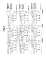
- FIG. 7 illustrates an equivalent circuit of pixels of an imaging device. Portions similar to those of FIG. 1 are designated by the same numerals.
- Each pixel 20 includes a discharge switch 18 .
- the discharge switch 18 discharges an electric charge in the photoelectric conversion portion 1 to a power supply node 15 such as an overflow drain.
- a control line OFG is connected to the discharge switch 18 .
- the discharge switch 18 is a MOS transistor, for example.
- the first transfer switch 4 is controlled to shift from an on-state to an off-state, whereby the photoelectric conversion portion 1 starts accumulating an electric charge.
- the discharge switch 18 it is also possible to control the discharge switch 18 to start an exposure. More specifically, the discharge switch 18 is controlled to shift from an on-state to an off-state, whereby the photoelectric conversion portion 1 starts accumulating an electric charge. With this operation, it is possible to arbitrarily set the exposure time.
- the configuration is such that in a part of the second period, the first transfer switch 4 is off, and the first transfer switch 4 is also driven three times. With this operation, it is possible to treat electric charges corresponding to a maximum of three times as much as those in the photoelectric conversion portion 1 .
- FIGS. 2A, 2B, 2C, and 3 illustrate cross-sectional structures and a top view of pixels of the imaging device according to the present exemplary embodiment.
- the descriptions of FIGS. 2A, 2B, 2C , and 3 are similar to those in the first exemplary embodiment and therefore are omitted.
- the discharge switch 18 discharges an electric charge in the photoelectric conversion portion 1 to the overflow drain 15 to which a predetermined voltage is supplied.
- FIG. 8 schematically illustrates driving pulses used in the present exemplary embodiment.
- FIG. 8 illustrates driving pulses supplied to the control line Tx 1 , the control line Tx 2 , and the control line OFG of each pixel in m ⁇ 1-th to m+1-th rows.
- the driving pulse supplied to the control line Tx 2 is similar to that in the first exemplary embodiment.
- driving pulses are supplied from a control unit disposed in the imaging device.
- a control unit a logic circuit such as a shift register or an address decoder is used.
- the discharge switch 18 is controlled to shift from an on-state to an off-state. While the discharge switch 18 is on, a generated electric charge is discharged.
- the exposure period is from the time T 4 to a time T 3 .
- the control line Tx 1 is driven a plurality of times, thereby transferring an electric charge from the photoelectric conversion portion 1 to the holding portion 2 a plurality of times.
- a single exposure period is the total of the period from the time T 4 to a time TA 1 (exposure period for a single transfer), the period from the time TA 1 to a time TA 2 , and the period from the time TA 2 to a time TA 3 .
- the period from the time T 4 to the time TA 1 corresponds to the first period in FIG. 4 . Further, the period from the time TA 1 to the time TA 3 corresponds to the second period in FIG. 4 .
- the time TA 3 and the time T 3 are the same time. To reduce the unevenness of accumulation in the respective exposure periods, it is desirable to set approximately equal periods as the exposure periods. Further, to shorten the exposure periods, the time T 4 may be set to, for example, the second period described in the first exemplary embodiment.
- the driving pulses in FIG. 4 can be used.
- the driving pulses in FIG. 8 can be used.
- driving pulses obtained by setting the time T 4 in FIG. 8 to a later time can be used.
- the photoelectric conversion portion 1 starts accumulating an electric charge. Then, from the time T 4 to the time T 3 , the discharge switch is maintained in the off-state. Further, a reading operation is performed based on the driving pulses illustrated in FIG. 5 .
- FIG. 9 schematically illustrates an operation of the imaging device.
- FIG. 9 illustrates an imaging operation from an n-th frame to an n+1-th frame.
- the operation regarding the n-th frame is indicated by a solid line, and the operation regarding the n+1-th frame is indicated by a dotted line.
- FIG. 9 illustrates the exposure period, the period during which the photoelectric conversion portion 1 accumulates an electric charge, and the period during which the holding portion 2 holds an electric charge, for each frame. Further, FIG. 9 illustrates a state where, in the first period, a reading operation is performed on the plurality of pixels.
- the reading operation in FIG. 9 refers to an operation including the transfer of an electric charge by the second transfer switch 5 and the output of a signal from the amplification unit 10 , which have been described with reference to FIG. 5 .
- the reading operation is performed only on each of some of the pixels included in the imaging device.
- a single exposure period is the total of the first and second periods. At this time, an electric charge in the previous frame held in the holding portion 2 is read in or before the first period. Thus, if the first period ends, the holding portion 2 can hold an electric charge. Therefore, the photoelectric conversion portion 1 only needs to be able to accumulate at least an electric charge generated during the first period.
- the amount of electric charge generated during the first period is smaller than the amount of electric charge generated during the single exposure period. Thus, it is possible to make the amount of saturation charge of the photoelectric conversion portion 1 small.
- the ratio of the total of the first and second periods to the first period should be substantially equal to the ratio of the amount of saturation charge of the holding portion 2 to the amount of saturation charge of the photoelectric conversion portion 1 .
- the total of the first and second periods refers to the single exposure period.
- the ratio of the single exposure period to the first period is 3.
- the first period is 1 ⁇ 3 of the single exposure period.
- the discharge period during which the discharge switch 18 is on is almost equal to the first period. For example, in a case where a moving image of 60 frames per second is captured, the first period is 1/240 seconds.
- the ratio of the amount of saturation charge of the holding portion 2 to the amount of saturation charge of the photoelectric conversion portion 1 should be close to 3. This is because the photoelectric conversion portion 1 only needs to hold electric charges of which the amount is 1 ⁇ 3 of the electric charges generated during the single exposure period, whereas the holding portion 2 holds all electric charges generated during the single exposure period. With such a ratio between the amounts of saturation charge, it is possible to optimize the sizes of the photoelectric conversion portion 1 and the holding portion 2 .
- a third exemplary embodiment is described.
- the present exemplary embodiment is different from the first and second exemplary embodiments in the configuration of a pixel for detecting a phase difference on an imaging plane.
- first and second exemplary embodiments are described, and portions similar to those of the first or second exemplary embodiment are not described here.
- FIG. 10 illustrates an equivalent circuit of pixels of an imaging device. Portions similar to those of FIG. 1 are designated by the same numerals.
- FIG. 10 is different from FIG. 1 in that the photoelectric conversion portion 1 includes a plurality of accumulation regions.
- the circuit diagram in FIG. 10 illustrates the plurality of accumulation regions as photoelectric conversion portions 1 a and 1 b for convenience.
- two holding portions 2 corresponds to the plurality of accumulation regions.
- two first transfer switches 4 may be included.
- the holding portion 2 includes a plurality of holding regions corresponding to the plurality of accumulation regions.
- the circuit diagram in FIG. 10 illustrates the plurality of holding regions as holding portions 2 a and 2 b for convenience.
- the first transfer switch 4 includes a plurality of first transfer transistors 4 a and 4 b corresponding to the plurality of accumulation regions. Further, the second transfer switch includes a plurality of second transfer transistors 5 a and 5 b corresponding to the plurality of holding regions.
- a pixel can output a signal for focus detection by the image plane phase difference method. For example, in a case where the photoelectric conversion portions 1 a and 1 b are placed to be arranged to the left and right, it is possible to output a signal for detecting the phase difference in the left-right direction.
- the input node 3 of the amplification unit 10 and the subsequent members and operations are similar to those in FIG. 1 and therefore are not described here.
- the photoelectric conversion portions 1 a and 1 b can accumulate electric charges generated while the holding portion 2 holds an electric charge. Therefore, it is possible to perform both an imaging operation in which the periods of photoelectric conversion in a plurality of pixels coincide with each other, i.e., a so-called global electronic shutter, and phase difference detection.
- FIG. 11 schematically illustrates a cross-sectional structure of the imaging device. Portions having functions similar to those in FIG. 10 are designated by the same numerals. Further, portions having functions similar to those in FIGS. 2A, 2B, and 2C are designated by the same numerals. However, two photoelectric conversion portions 1 , two holding portions 2 , two first transfer switches 4 , and two second transfer switches 5 are disposed. Therefore, alphabetical letters are added to the end of the numbers to distinguish these from each other.
- a pixel 20 includes a photoelectric conversion portion 1 a , which includes an accumulation region 11 a , and a photoelectric conversion portion 1 b , which includes an accumulation region 11 b .
- the pixel 20 includes two photoelectric conversion portions. More specifically, the pixel 20 includes a single photoelectric conversion portion, and the single photoelectric conversion portion includes accumulation regions 11 a and 11 b . As illustrated in FIG. 11 , the accumulation regions 11 a and 11 b are disposed under a single microlens 101 . Between the accumulation regions 11 a and 11 b , a separation region 19 is provided.
- the separation region 19 includes a P-type semiconductor region. The separation region 19 is not necessarily formed with a uniform impurity concentration.
- a part of the separation region 19 may be formed with a low concentration, or may be an N-type semiconductor region.
- the separation region 19 electrically separates the accumulation regions 11 a and 11 b from each other.
- FIG. 11 illustrates an imaging device of a front-side illumination type. Alternatively, an imaging device of a back-side illumination type may be used.
- the other members are similar to those in FIGS. 2A, 2B, and 2C and therefore are not described here.
- FIG. 12 schematically illustrates an upper surface structure of the imaging device. Portions having functions similar to those in FIGS. 10 and 11 are designated by the same numerals. Further, portions having functions similar to those in FIG. 3 are designated by the same numerals. However, two photoelectric conversion portions 1 , two holding portions 2 , two first transfer switches 4 , and two second transfer switches 5 are disposed. Thus, alphabetical letters are added to the end of the numbers to distinguish these from each other.
- FIG. 11 illustrates a cross section taken along a line A-B in FIG. 12 .
- a pixel 20 includes photoelectric conversion portions 1 a and 1 b .
- the pixel 20 includes holding portions 2 a and 2 b .
- the pixel 20 includes first transfer transistors 4 a and 4 b .
- the pixel 20 includes second transfer transistors 5 a and 5 b .
- the pixel 20 includes two floating diffusion (FD) regions, which form an input node 3 of an amplification unit. The two FD regions are connected to each other via wiring (not illustrated).
- FD floating diffusion
- the pixel 20 can be used as a pixel for phase difference detection in the left-right direction.
- the other members are similar to those in FIG. 3 and therefore are not described here.
- the arrangement of the members and the shape of the light shielding portion are not limited to this example, and each member is appropriately placed.
- all the pixels are pixels for focus detection.
- only some of the plurality of pixels include a plurality of photoelectric conversion portions 1 a and 1 b .
- the other pixels include only a single photoelectric conversion portion 1 . This variation is suitable for a case where only signals from some of the pixels are used for focus detection.
- the configuration is illustrated in which the photoelectric conversion portion is divided into left and right portions.
- the configuration may be such that the photoelectric conversion portion is also divided into upper and lower portions to detect the phase difference between the upper and lower portions. Yet alternatively, both of these configurations may be included. More specifically, in a first pixel, a plurality of photoelectric conversion portions 1 a and 1 b are arranged along a first direction. In a second pixel, a plurality of photoelectric conversion portions 1 a and 1 b are arranged along a second direction intersecting the first direction. Further, the configuration may be such that the photoelectric conversion portion is divided into three or more portions to detect the phase difference more accurately, or the configuration may be such that the size of each photoelectric conversion portion is changed according to an arrangement location in the pixel region.
- the holding portions 2 a and 2 b should have a large amount of saturation charge as the total amount of saturation charge of the holding portions 2 a and 2 b .
- the impurity concentration of the N-type semiconductor region 201 of each of the holding portions 2 a and 2 b is made high, or the area of the N-type semiconductor region 201 in a plan view is made large, whereby it is possible to increase the amounts of saturation charge of the holding portions 2 a and 2 b .
- the impurity concentration of the N-type semiconductor region 201 is high, a leakage current is likely to become large, and therefore, noise may become large.
- the area of the N-type semiconductor region 201 in a plan view is made large, whereby it is possible to increase the amount of saturation charge while reducing the impurity concentration of the N-type semiconductor region 201 .
- the area of each of the holding portions 2 a and 2 b in a plan view i.e., the area of the orthogonal projection of each of the holding portions 2 a and 2 b , is made large, whereby it is possible to increase the amount of saturation charge of the pixel while reducing noise. Consequently, the area of each of the photoelectric conversion portions 1 a and 1 b in a plan view is likely to be relatively small, and it is difficult to increase the amounts of saturation charge of the photoelectric conversion portions 1 a and 1 b . This makes the effect more prominent that even if the amounts of saturation charge of the photoelectric conversion portions 1 a and 1 b are small, it is possible to maintain the amount of saturation charge of the pixel.
- FIG. 13 schematically illustrates driving pulses used in the present exemplary embodiment.
- FIG. 13 illustrates a driving pulse supplied to the first transfer transistor 4 a , a driving pulse supplied to the first transfer transistor 4 b , a driving pulse supplied to the second transfer transistor 5 a , and a driving pulse supplied to the second transfer transistor 5 b .
- a driving pulse is at a high level, the corresponding transistor or switch is turned on.
- a driving pulse is at a low level, the corresponding transistor or switch is turned off.
- These driving pulses are supplied from a control unit disposed in the imaging device.
- the control unit a logic circuit such as a shift register or an address decoder is used.
- the first transfer transistors 4 a and 4 b operate in a same phase with each other.
- the driving pulse supplied to the transistor 4 a and the driving pulse supplied to the first transfer transistor 4 b are collectively described. According to such a configuration, it is possible to make the accumulation times of two photoelectric conversion portions equal. Thus, it is possible to improve the accuracy of detecting a phase difference. In a case where the accumulation times do not necessarily need to be made equal, it is also possible to appropriately change the operation timing of the two first transfer transistors 4 a and 4 b . Further, the second transfer transistors 5 a and 5 b are controlled independently of each other.
- the driving method according to the present exemplary embodiment is similar to that in FIG. 4 , except that when a signal is read for each pixel, the second transfer transistors 5 a and 5 b are sequentially turned on. Therefore, portions similar to those in FIG. 4 are not described here.
- FIG. 14 schematically illustrates driving pulses used by the imaging device.
- FIG. 14 is different from FIG. 5 in that a driving pulse Tx 2 a , which is supplied to the second transfer transistor 5 a , and a driving pulse Tx 2 b , which is supplied to the second transfer transistor 5 b , are included.
- a driving pulse SEL, which is supplied to the selection transistor 7 , and a driving pulse RES, which is supplied to the reset transistor 9 are similar to those in FIG. 5 .
- a driving pulse is at a high level, the corresponding transistor or switch is turned on.
- a driving pulse is at a low level, the corresponding transistor or switch is turned off.
- FIG. 14 illustrates a noise signal NA, which is read for the first time, a signal NB, which is read for the second time, and optical signals SA and SB.
- An output signal may be subjected to AD conversion outside the imaging device, or may be subjected to AD conversion inside the imaging device. Further, the reading order of the two holding portions 2 a and 2 b may be reversed. Further, it is also possible to speed up the operation by, for example, omitting the reading of a noise signal for the second time.
- FIG. 6 schematically illustrates an operation of the imaging device, similar to the first exemplary embodiment.
- FIG. 6 illustrates an imaging operation from an n-th frame to an n+1-th frame.
- the operation regarding the n-th frame is indicated by a solid line, and the operation regarding the n+1-th frame is indicated by a dotted line.
- FIG. 6 illustrates an exposure period, the period during which the photoelectric conversion portion 1 (the operations of the photoelectric conversion portions 1 a and 1 b are collectively described as a similar operation) accumulates an electric charge, and the period during which the holding portion 2 (the operations of the holding portions 2 a and 2 b are collectively described as a similar operation) holds an electric charge, for each frame.
- FIG. 6 illustrates a state where, in the first period, a reading operation is performed on the plurality of pixels.
- the reading operation in FIG. 6 refers to an operation including the transfer of an electric charge by the second transfer transistor 5 a or 5 b and the output of a signal from the amplification unit 10 , which have been described with reference to FIGS. 13 and 14 .
- the next exposure can be started. Therefore, it is possible to substantially eliminate the period of missing information. Thus, it is possible to improve image quality.
- the reading operation is performed on each of the plurality of pixels. Therefore, even if the amount of saturation charge of the photoelectric conversion portion 1 is small, it is possible to increase the amount of saturation charge of the pixel.
- the amount of saturation charge of the pixel is the maximum value of the amount of electric charge that can be treated as signals among electric charges generated in a single exposure.
- the amount of saturation charge of the photoelectric conversion portion 1 is the maximum value of the total amount of electric charge that can be accumulated in the photoelectric conversion portions 1 a and 1 b
- the amount of saturation charge of the holding portion 2 is the maximum value of the total amount of electric charge that can be held in the holding portions 2 a and 2 b
- the amount of saturation charge of the holding portion 2 a is defined by the difference between the depletion voltage of the photoelectric conversion portion 1 a and the depletion voltage of the holding portion 2 a
- the amount of saturation charge of the holding portion 2 b is defined by the difference between the depletion voltage of the photoelectric conversion portion 1 b and the depletion voltage of the holding portion 2 b.
- a single exposure period is the total of the first and second periods. At this time, an electric charge in the previous frame held in the holding portion 2 is read in the first period. Thus, if the first period ends, the holding portion 2 can hold an electric charge. Thus, the photoelectric conversion portion 1 only needs to be able to accumulate at least an electric charge generated during the first period. Typically, the amount of electric charge generated during the first period is smaller than the amount of electric charge generated during the single exposure period. Thus, it is possible to make the amount of saturation charge of the photoelectric conversion portion 1 small.
- the first period during which the photoelectric conversion portion 1 accumulates an electric charge is almost equal to the second period during which the holding portion 2 holds an electric charge.
- the second period during which the holding portion 2 holds an electric charge may be longer than the first period.
- the first period may be longer than the second period.
- FIG. 6 illustrates an example where the reading operation is performed in order from the first row.
- the order of performing the reading operation is not limited to this example.
- reading may only need to be performed at least once on each of the pixels included in a single frame.
- the period from when the holding portion 2 starts holding an electric charge in a certain frame to when the holding portion 2 starts holding an electric charge for the next frame is equal to the exposure period.
- the ratio of the total of the first and second periods to the first period should be almost equal to the ratio of the amount of saturation charge of the holding portion 2 to the amount of saturation charge of the photoelectric conversion portion 1 .
- the total of the first and second periods refers to the single exposure period.
- the ratio of the single exposure period to the first period is 2.
- the first period is 1 ⁇ 2 of the single exposure period.
- the first period is 1/120 seconds.
- the ratio of the amount of saturation charge of the holding portion 2 to the amount of saturation charge of the photoelectric conversion portion 1 should be close to 2. This is because the photoelectric conversion portion 1 only needs to hold electric charges of which the amount is 1 ⁇ 2 of the electric charges generated during the single exposure period, whereas the holding portion 2 holds all electric charges generated during the single exposure period. With such a ratio between the amounts of saturation charge, it is possible to optimize the sizes of the photoelectric conversion portion 1 and the holding portion 2 .
- the imaging device may have an operation mode for performing a rolling shutter.
- the photoelectric conversion portions 1 of the plurality of pixels sequentially start accumulating electric charges.
- the first transfer switches 4 of the plurality of pixels are sequentially controlled to be turned on.
- the imaging device may have an operation mode for performing a global electronic shutter of another method.
- the global electronic shutter of another method refers to an operation in which the period during which the photoelectric conversion portion 1 accumulates an electric charge is equal to the exposure period.
- the imaging device of the present exemplary embodiment it is possible to perform a global electronic shutter while improving the amount of saturation charge. Further, at the same time, it is also possible to output signals for phase difference detection of which the accumulation times are equal.
- a fourth exemplary embodiment is described.
- the present exemplary embodiment is different from the third exemplary embodiment in that a pixel includes a discharge switch. Therefore, only the differences from the third exemplary embodiment are described, and portions similar to those of the third exemplary embodiment are not described here.
- FIG. 15 illustrates an equivalent circuit of pixels of an imaging device. Portions similar to those of FIG. 10 are designated by the same numerals.
- Each photoelectric conversion portion 1 a includes a discharge switch 18 a
- each photoelectric conversion portion 1 b includes a discharge switch 18 b
- the discharge switches 18 a and 18 b discharge electric charges in the photoelectric conversion portions 1 a and 1 b to power supply nodes 15 a and 15 b such as overflow drains, respectively.
- a control line OFG is connected to the discharge switches 18 a and 18 b .
- Each of the discharge switches 18 a and 18 b is a MOS transistor, for example.
- the first transfer transistors 4 a and 4 b are controlled to shift from the on-state to off-state, whereby the photoelectric conversion portions 1 a and 1 b start accumulating electric charges.
- the discharge switches 18 a and 18 b are controlled to shift from the on-state to off-state, whereby the photoelectric conversion portions 1 a and 1 b start accumulating electric charges.
- the control line OFG is common to the discharge switches 18 a and 18 b .
- the configuration is such that during a part of the second period, the first transfer transistors 4 a and 4 b are off. Then, the photoelectric conversion portion 1 a transfers an electric charge to the holding portion 2 a three times, and the photoelectric conversion portion 1 b transfers an electric charge to the holding portion 2 b three times. With this operation, it is possible to treat electric charges corresponding to a maximum of three times as much as those in the photoelectric conversion portions 1 a and 1 b.
- FIG. 11 illustrates a cross-sectional structure of a pixel of the imaging device according to the present exemplary embodiment.
- the description of FIG. 11 is similar to that of the third exemplary embodiment and therefore is omitted.
- FIG. 16 illustrates a top view of pixels of the imaging device.
- FIG. 16 is different from FIG. 12 of the third exemplary embodiment in that the discharge switches 18 a and 18 b are added between the photoelectric conversion portions 1 a and 1 b .
- the other members are similar to those of the third exemplary embodiment and therefore are not described here.
- FIG. 11 illustrates a cross section taken along a line A-B in FIG. 16 .
- the discharge switches 18 a and 18 b discharge electric charges in the photoelectric conversion portions 1 a and 1 b to the overflow drains 15 a and 15 b , respectively, to which a predetermined voltage is supplied.
- FIG. 17 schematically illustrates driving pulses used in the present exemplary embodiment.
- FIG. 17 illustrates driving pulses supplied to control lines Tx 1 a and Tx 1 b , control lines Tx 2 a and Tx 2 b , and the control line OFG of each pixel in m ⁇ 1-th to m+1-th rows.
- the driving pulses supplied to the control lines Tx 2 a and Tx 2 b are similar to those of the third exemplary embodiment illustrated in FIG. 14 .
- driving pulses are supplied from a control unit disposed in the imaging device.
- a control unit a logic circuit such as a shift register or an address decoder is used.
- the discharge switches 18 a and 18 b are controlled to shift from an on-state to off-state. While the discharge switches 18 a and 18 b are on, generated electric charges are discharged.
- the exposure period is from the time T 4 to a time T 3 .
- the control lines Tx 1 a and Tx 1 b are driven a plurality of times, thereby sequentially transferring electric charges in the photoelectric conversion portions 1 a and 1 b to the holding portions 2 a and 2 b , respectively.
- Exposure periods are from the time T 4 to a time TA 1 , from the time TA 1 to a time TA 2 , and from the time TA 2 to a time TA 3 .
- the time TA 3 and the time T 3 are the same time. To reduce the unevenness of accumulation during the exposure periods, it is desirable to set approximately equal periods. Further, to shorten the exposure periods, the time T 4 may be set to, for example, the second period described in the third exemplary embodiment.
- the driving pulses in FIG. 13 can be used.
- the driving pulses in FIG. 17 can be used.
- driving pulses obtained by setting the time T 4 in FIG. 17 to a later time can be used.
- the photoelectric conversion portions 1 a and 1 b start accumulating electric charges. Then, from the time T 4 to the time T 3 , the discharge switches 18 a and 18 b are maintained in the off-states. Further, a reading operation is performed based on the driving pulses illustrated in FIG. 5 .
- a fifth exemplary embodiment is described.
- the present exemplary embodiment is different from the fourth exemplary embodiment in the circuit configuration of a pixel. Therefore, only the differences from the fourth exemplary embodiment are described, and portions similar to those of the fourth exemplary embodiment are not described here.
- FIG. 18 illustrates an equivalent circuit according to the present exemplary embodiment.
- the input node 3 of the amplification unit 10 and the subsequent members are shared by the two second transfer transistors 5 a and 5 b . Therefore, a single amplification unit 10 receives electric charges from a plurality of accumulation regions.
- the amplification unit 10 includes a plurality of amplification transistors corresponding to a plurality of accumulation regions.
- the input node 3 of the amplification unit 10 is shared. Therefore, it is necessary to sequentially read accumulated electric charges in the holding portions 2 a and 2 b as illustrated in FIG. 14 .
- the configuration of FIG. 18 is employed, whereby the input node 3 and the subsequent members have individual configurations. Accordingly, it is possible to individually read accumulated electric charges in the holding portions 2 a and 2 b as illustrated in FIG. 5 of the first exemplary embodiment. As a result, it is possible to shorten the reading period, i.e., the first period. The first period is shortened, thereby shortening the period during which the photoelectric conversion portions 1 a and 1 b alone need to accumulate electric charges. Thus, it is possible to make the amounts of saturation charge of the photoelectric conversion portions 1 a and 1 b small and optimize the areas of the photoelectric conversion portions 1 a and 1 b and the holding portions 2 a and 2 b.
- FIG. 19 illustrates a top view of pixels according to the present exemplary embodiment.
- FIG. 19 is different from FIG. 16 of the fourth exemplary embodiment in that the discharge switches 18 a and 18 b are not arranged between the photoelectric conversion portions 1 a and 1 b , but are arranged symmetrically with respect to a separation region. Since overflow drains 15 are formed separately from each other, there is an advantage that it is easy to independently control discharge. It is a matter of course that even if a configuration similar to that in FIG. 16 is employed, the operation illustrated in the present exemplary embodiment is similarly performed. Thus, it is possible to select an appropriate configuration.
- a driving method according to the present exemplary embodiment is similar to those according to the third and fourth exemplary embodiments. More specifically, if discharge switches are not included, the driving pulses and the operations illustrated in FIGS. 13 and 6 are used. If discharge switches are included, the driving pulses and the operations illustrated in FIGS. 17 and 9 are used. A detailed description is similar to those in the third and fourth exemplary embodiments and therefore is omitted.
- a sixth exemplary embodiment is described.
- the present exemplary embodiment is different from the first to fifth exemplary embodiments in the driving method. Therefore, only the differences from the first to fifth exemplary embodiments are described, and portions similar to those of any of the first to fifth exemplary embodiments are not described here.
- FIGS. 1, 7, 10, 15, and 18 illustrates an equivalent circuit of pixels of an imaging device according to the present exemplary embodiment.
- the descriptions of these figures have been already made above in the first to fifth exemplary embodiments and therefore are omitted.
- a cross-sectional structure of a pixel of the present exemplary embodiment is also similar to that of any of the first to fifth exemplary embodiments.
- any of FIGS. 2A, 2B, 2C, and 11 schematically illustrates a cross-sectional structure of a pixel of the present exemplary embodiment. The descriptions of these figures have been already made above in the first to fifth exemplary embodiments and therefore are omitted.
- FIG. 20 schematically illustrates an operation used in the present exemplary embodiment.
- FIG. 20 is different from FIGS. 6 and 9 of the first to fifth exemplary embodiments in the operation of reading rows, i.e., the operation in the first period.
- FIG. 20 illustrates an operation of reading pixel signals of any row first, which is a row including pixel signals for phase difference detection in this case, and then reading pixel signals of the other rows.
- the pixel signals used for phase difference detection are output before the reading of the pixel signals of all the rows is finished. Therefore, it is possible to perform the processing of phase difference detection earlier. As a result, it is possible to perform phase difference detection at a higher speed.
- the row used for phase difference detection read out first is skipped in the reading of the subsequent other rows, but may be sequentially read out again.
- pixel signals are output sequentially from the rows.
- Detailed driving pulses are similar to those in any of the first to fifth exemplary embodiments and therefore are not described here. If a pixel does not include a discharge switch 18 , a driving pulse supplied to the control line OFG is not necessary.
- FIG. 21 illustrates a block diagram of a digital still camera as an example of the imaging system.
- a barrier 1001 protects a lens.
- a lens 1002 forms an optical image of an object on an imaging device 1004 .
- a diaphragm 1003 varies the amount of light passing through the lens 1002 .
- the imaging device 1004 is the imaging device described in each of the above exemplary embodiments and converts the optical image formed by the lens 1002 into image data. At this time, it is assumed that an AD conversion unit is formed on a semiconductor substrate of the imaging device 1004 .
- a signal processing unit 1007 makes various corrections on captured data output from the imaging device 1004 and compresses data. Then, in FIG. 21 , a timing generation unit 1008 outputs various timing signals to the imaging device 1004 and the signal processing unit 1007 .
- An overall control unit 1009 controls the entire digital still camera.
- a frame memory unit 1010 temporarily stores image data.
- An interface unit 1011 is an interface for recording or reading data into or from a recording medium.
- An attachable and detachable recording medium 1012 such as a semiconductor memory is used to record or read captured data therein or therefrom.
- an interface unit 1013 is an interface used to communicate with an external computer.
- a timing signal may be input from outside the imaging system.
- the imaging system may only need to include at least the imaging device 1004 and the signal processing unit 1007 for processing an imaging signal output from the imaging device 1004 .
- the configuration has been described in which the imaging device 1004 and the AD conversion unit are formed on the same semiconductor substrate.
- the imaging device 1004 and the AD conversion unit may be provided on different semiconductor substrates.
- the imaging device 1004 and the signal processing unit 1007 may be formed on the same semiconductor substrate.
Landscapes
- Engineering & Computer Science (AREA)
- Multimedia (AREA)
- Signal Processing (AREA)
- Transforming Light Signals Into Electric Signals (AREA)
- Solid State Image Pick-Up Elements (AREA)
Abstract
The imaging device performs a global electronic shutter operation in which exposure periods of a plurality of pixels coincide with each other. In a first period during which a photoelectric conversion portion of at least one of the pixels accumulates an electric charge, signals based on electric charges held in holding portions of the plurality of pixels are sequentially output to an output line. During a second period after the output of the signals from the plurality of pixels is finished, the holding unit of each of the plurality of pixels holds an electric charge.
Description
Technique Field
The present disclosure relates to an imaging device and an imaging system.
Description of the Related Art
In recent years, a method for using a global electronic shutter in a complementary metal-oxide-semiconductor (CMOS) image sensor is discussed. Each of imaging devices discussed in Japanese Patent Application Laid-Open No. 2004-111590 and Japanese Patent Application Laid-Open No. 2006-246450 has the advantage that even if a quickly moving object is captured, an object image is not distorted. Further, Japanese Patent Application Laid-Open No. 2007-325139 discusses an imaging device that performs focus detection by a pupil division phase difference method.
According to a first aspect of the embodiment, an imaging device includes a plurality of pixels each including a photoelectric conversion portion configured to accumulate an electric charge generated with incident light, a holding unit configured to hold the electric charge, an amplification unit configured to output a signal based on the electric charge, a first transfer switch configured to transfer the electric charge from the photoelectric conversion portion to the holding unit, and a second transfer switch configured to transfer the electric charge from the holding unit to the amplification unit, and an output line to which signals from the amplification units of the plurality of pixels are output, wherein the photoelectric conversion portion of each of at least some pixels of the plurality of pixels includes a plurality of accumulation regions electrically isolated from each other, wherein at a first time, the photoelectric conversion portions of the plurality of pixels starts accumulating the electric charge, wherein from the first time to a second time, the first transfer switch of at least one pixel of the plurality of pixels is maintained in an off-state, and the photoelectric conversion portion of the at least one pixel accumulates an electric charge generated during a first period from the first time to the second time, wherein in the first period, the second transfer switches of the plurality of pixels are turned on in turns, and the amplification units of the plurality of pixels output signals in turns, wherein during at least a part of a second period from the second time to a third time, the holding unit of each of the plurality of pixels holds an electric charge generated during the first period in the photoelectric conversion portion and an electric charge generated during the second period in the photoelectric conversion portion, and wherein at the third time, the first transfer switches of the plurality of pixels are controlled to shift from an on-state to an off-state.
According to a second aspect of the present invention, an imaging device includes a plurality of pixels each including a photoelectric conversion portion configured to accumulate an electric charge generated by incident light, a holding unit configured to hold the electric charge, an amplification unit configured to output a signal based on the electric charge, a first transfer switch configured to transfer the electric charge from the photoelectric conversion portion to the holding unit, and a second transfer switch configured to transfer the electric charge from the holding unit to the amplification unit, an output line to which signals from the amplification units of the plurality of pixels are output, and light shielding portions configured to shield the photoelectric conversion portions of a pair of pixels included in the plurality of pixels from light so that the photoelectric conversion portions of the pair of pixels receive light passing through positions different from each other in a pupil, wherein at a first time, the photoelectric conversion portions of the plurality of pixels starts accumulating the electric charge, wherein from the first time to a second time, the first transfer switch of at least one pixel of the plurality of pixels is maintained in an off-state, and the photoelectric conversion portion of the at least one pixel accumulates an electric charge generated during a first period from the first time to the second time, wherein in the first period, the second transfer switches of the plurality of pixels are turned on in turns, and the amplification units of the plurality of pixels output signals in turns, wherein during at least a part of a second period from the second time to a third time, the holding unit of each of the plurality of pixels holds an electric charge generated during the first period in the photoelectric conversion portion and an electric charge generated during the second period in the photoelectric conversion portion, and wherein at the third time, the first transfer switches of the plurality of pixels are controlled to shift from an on-state to an off-state.
According to a third aspect of the present invention, an imaging device includes a plurality of pixels, each including a photoelectric conversion portion configured to accumulate an electric charge generated by incident light, a holding unit configured to hold the electric charge, an amplification unit configured to output a signal based on the electric charge, a first transfer switch configured to transfer the electric charge from the photoelectric conversion portion to the holding unit, and a second transfer switch configured to transfer the electric charge from the holding unit to the amplification unit; and an output line to which signals from the amplification units of the plurality of pixels are output, wherein at a first time, the photoelectric conversion portions of the plurality of pixels starts accumulating the electric charge, wherein from the first time to a second time, the first transfer switch of at least one pixel of the plurality of pixels is maintained in an off-state, and the photoelectric conversion portion of the at least one pixel accumulates an electric charge generated during a first period from the first time to the second time, wherein during the first period, the second transfer switches of the plurality of pixels are turned on in turns, and the amplification units of the plurality of pixels output signals in turns, wherein during at least a part of a second period from the second time to a third time, the holding unit of each of the plurality of pixels holds an electric charge generated during the first period in the photoelectric conversion portion and an electric charge generated during the second period in the photoelectric conversion portion, wherein at the third time, the first transfer switches of the plurality of pixels are controlled to shift from an on-state to an off-state, and wherein each of at least some pixels of the plurality of pixels outputs a signal for focus detection by an image plane phase difference method.
Further features of the present invention will become apparent from the following description of exemplary embodiments with reference to the attached drawings.
According to some embodiments, it is possible to improve the amount of saturation charge while performing a global electronic shutter operation. Further, it is possible to perform image plane phase difference autofocus on an imaging plane.
Each of the imaging device discussed in Japanese Patent Application Laid-Open No. 2004-111590 and the imaging device discussed in Japanese Patent Application Laid-Open No. 2007-325139 accumulates in a photoelectric conversion portion all electric charges generated through photoelectric conversion for obtaining a single image or a single frame. Then, the imaging device transfers the electric charges in all pixels from the photoelectric conversion portion to a holding unit simultaneously and starts photoelectric conversion for obtaining the next image or the next frame. Therefore, to increase the amount of saturation charge of a pixel, it is necessary to secure both the amount of saturation charge of the photoelectric conversion portion and the amount of saturation charge of the holding unit to be almost the same amount. If the amount of saturation charge of the photoelectric conversion portion is made large, the area of the photoelectric conversion portion increases. As a result, the size of the pixel becomes large.
The imaging device discussed in Japanese Patent Application Laid-Open No. 2006-246450 holds almost all electric charges in a holding unit by hardly accumulating an electric charge in a photoelectric conversion portion. Therefore, it is possible to increase the amount of saturation charge of a pixel without increasing the amount of saturation charge of the photoelectric conversion portion. In this method, however, a period during which a generated electric charge cannot be accumulated occurs. Therefore, the image quality may decrease.
As described above, with the imaging devices known to the inventors, it is difficult to make the amount of saturation charge of a pixel large. In view of the above problems, some embodiments enable improvement in the amount of saturation charge of a pixel in an imaging device capable of performing a global electronic shutter operation.
One embodiment according to the present invention is an imaging device including a plurality of pixels and an output line to which signals from the plurality of pixels are output. Each of the plurality of pixels includes a photoelectric conversion portion, a holding unit configured to hold an electric charge, and an amplification unit configured to output a signal based on the electric charge. Further, a first transfer switch configured to transfer the electric charge from the photoelectric conversion portion to the holding unit, and a second transfer switch configured to transfer the electric charge from the holding unit to the amplification unit are arranged. With such a configuration, it is possible to perform an imaging operation in which the periods of photoelectric conversion in a plurality of pixels coincide with each other, i.e., a so-called global electronic shutter operation. An electronic shutter operation refers to electrical control of the accumulation of an electric charge generated by incident light.
Further, at least some of the pixels output signals for focus detection by an image plane phase difference method. Thus, it is possible to perform a global electronic shutter operation and also achieve phase difference autofocus on an imaging plane. In some embodiments, the photoelectric conversion portion of each pixel includes a plurality of accumulation regions electrically isolated, or separated, from each other. With such a configuration, the pixel can output a signal for focus detection by the image plane phase difference method. Further, in some embodiments, light shielding portions configured to shield the photoelectric conversion portions included in a pair of pixels from light are provided to photoelectric conversion portion so that the photoelectric conversion portions of the pair of pixels receive light passing through positions different from each other in a pupil. With such a configuration, each of the pair of pixels can output a signal for focus detection by the image plane phase difference method.
In some embodiments according to the present invention, at a first time, the photoelectric conversion portions of the plurality of pixels simultaneously start accumulating electric charges. From the first time to a second time, the first transfer switch of at least one of the pixels is maintained in an off-state. In the at least one pixel, the photoelectric conversion portion accumulates an electric charge generated during this period. The period from the first time to the second time is a first period.
In the first period, signals based on electric charges held in the holding portions of the plurality of pixels are sequentially output from the amplification units to the output line. In other words, in the first period, each pixel outputs a signal at least once. As a specific operation, in the first period, the second transfer switches of the plurality of pixels are sequentially turned on. An electric charge generated during the first period is accumulated in the photoelectric conversion portion. Thus, during the first period, the holding unit can hold an electric charge generated before the first time.
The number of signals to be output in the first period can be changed depending on the format of an image to be output. For example, if a moving image is captured, as many signals as the number of horizontal lines used in a single frame may only need to be output. In such an embodiment, signals may not need to be output from all the pixels included in the imaging device.
After the output of the signals from the plurality of pixels is finished, during at least a part of a second period from the second time to a third time, the holding unit of each of the plurality of pixels holds an electric charge. At this time, the holding unit holds an electric charge generated during the first period and an electric charge generated during the second period. At the third time, the first transfer switches of the plurality of pixels are simultaneously controlled to shift from on-states to off-states.
The photoelectric conversion portion only needs to be able to accumulate at least an electric charge generated during the first period. Therefore, even if the amount of saturation charge of the photoelectric conversion portion is small, it is possible to maintain the amount of saturation charge of the pixel. Thus, with such a configuration, it is possible to perform a global electronic shutter operation while maintaining the amount of saturation charge. In some embodiments, the second period during which the holding unit of each of the plurality of pixels holds an electric charge is longer than the first period. This is because, since the second period is longer than the first period, it is possible to make the amount of saturation charge of the photoelectric conversion portion smaller.
With reference to the drawings, exemplary embodiments of the present invention will be described below. It is a matter of course that the exemplary embodiments according to the present invention are not limited only to the exemplary embodiments described below. For example, an example where the configuration of a part of any of the exemplary embodiments is added to another of the exemplary embodiments, or an example where the configuration of a part of any of the exemplary embodiments is replaced with the configuration of a part of another of the exemplary embodiments is also an exemplary embodiment of the present invention. Further, in the following exemplary embodiments, a first conductive type is an N-type, and a second conductive type is a P-type. Alternatively, the first conductive type may be a P-type, and the second conductive type may be an N-type.
Now, a first exemplary embodiment is described. FIG. 1 illustrates an equivalent circuit of pixels of an imaging device. Although FIG. 1 illustrates nine pixels 20, the imaging device includes more pixels.
Each pixel 20 includes a photoelectric conversion portion 1, a holding portion 2, an amplification unit 10, a first transfer switch 4, and a second transfer switch 5. Further, the pixel 20 includes a reset transistor 9 and a selection transistor 7.
The photoelectric conversion portion 1 accumulates an electric charge generated by incident light. The first transfer switch 4 transfers the electric charge in the photoelectric conversion portion 1 to the holding portion 2. The holding portion 2 holds, at a location different from that of the photoelectric conversion portion 1, the electric charge generated by incident light. The second transfer switch 5 transfers the electric charge in the holding portion 2 to an input node 3 of the amplification unit 10. The reset transistor 9 resets the voltage of the input node 3 of the amplification unit 10. The selection transistor 7 selects a pixel 20 from which a signal is to be output to the output line 8. The amplification unit 10 outputs a signal based on the electric charge generated by incident light to the output line 8. The amplification unit 10 includes, for example, an amplification transistor forming a source follower. Further, each of the first transfer switch 4 and the second transfer switch 5 is a metal-oxide-semiconductor (MOS) transistor.
To the first transfer switch 4, a control line Tx1 is connected. To the second transfer switch 5, a control line Tx2 is connected. In the present exemplary embodiment, a plurality of pixels is arranged in a matrix. To pixels included in a single row, a common control line is connected. In the present exemplary embodiment, a control line connected to pixels in an m-th row, for example, is referred to as a “control line Tx1(m)”.
With such a configuration, the photoelectric conversion portion 1 can accumulate an electric charge generated while the holding portion 2 holds an electric charge. Therefore, it is possible to perform an imaging operation in which the periods of photoelectric conversion in a plurality of pixels coincide with each other, i.e., a so-called global electronic shutter operation.
In FIGS. 2A to 2C , the photoelectric conversion portion 1 has a buried-type photodiode structure. The photoelectric conversion portion 1 includes an N-type semiconductor region 11 and a P-type semiconductor region 12. The N-type semiconductor region 11 and the P-type semiconductor region 12 form a P-N junction. The P-type semiconductor region 12 can suppress noise in an interface.
The P-type semiconductor region 12 is a well. Under the N-type semiconductor region 11, an N-type semiconductor region 13 is disposed. The impurity concentration of the N-type semiconductor region 13 is lower than the impurity concentration of the N-type semiconductor region 11. With this configuration, an electric charge generated at a deep position is collected in the N-type semiconductor regions. In this case, the N-type semiconductor region 13 may be of a P-type. Under the N-type semiconductor region 13, a P-type semiconductor region 17 is disposed, which serves as a potential barrier against an electric charge.
The holding portion 2 includes an N-type semiconductor region 201 and a P-type semiconductor region 202. An electric charge to be a signal is held in the N-type semiconductor region 201. The impurity concentration of the N-type semiconductor region 201 is higher than the impurity concentration of the N-type semiconductor region 11. The P-type semiconductor region 202 is disposed on the N-type semiconductor region 201. The P-type semiconductor region 202 can suppress noise in an interface.
A gate electrode 40 forms the gate of the first transfer switch 4. Further, a gate electrode 50 forms the gate of the second transfer switch 5. In some variations, a part of the gate electrode 40 is disposed on the N-type semiconductor region 201 via a gate insulating film. In this case, the P-type semiconductor region 202 is not disposed between the gate electrode 40 and the N-type semiconductor region 201. A negative voltage is applied to the gate electrode 40, whereby it is possible to induce holes on the surface of the N-type semiconductor region 201. Consequently, it is possible to suppress noise generated in an interface.
The holding portion 2 is shielded from light by a light shielding portion 203. The light shielding portion 203 is formed of a metal less likely to allow visible light to pass therethrough, such as tungsten or aluminum. On an aperture of the light shielding portion 203, a color filter 100 and a microlens 101 are disposed.
The pixel 20 a illustrated in FIG. 2A does not output a signal for focus detection, and outputs a signal for imaging. The pixel 20 b illustrated in FIG. 2B and the pixel 20 c illustrated in FIG. 2C output signals for focus detection. An aperture A01 of the light shielding portion 203 of the pixel 20 a illustrated in FIG. 2A is larger than an aperture A02 of the light shielding portion 203 of the pixel 20 b illustrated in FIG. 2B . Further, the aperture A01 of the light shielding portion 203 of the pixel 20 a illustrated in FIG. 2A is larger than an aperture A03 of the light shielding portion 203 of the pixel 20 c illustrated in FIG. 2C . The aperture A02 of the light shielding portion 203 of the pixel 20 b and the aperture A03 of the light shielding portion 203 of the pixel 20 c are arranged so that the photoelectric conversion portions 1 of the pixels 20 b and 20 c receive light passing through positions different from each other in a pupil. For example, as illustrated in FIG. 2B , the aperture A02 of the light shielding portion 203 of the pixel 20 b is shifted to the right side with respect to the center of the photoelectric conversion portion 1. Comparing the pixels 20 a and 20 b, the aperture A02 of the light shielding portion 203 of the pixel 20 b corresponds to the right half of the aperture A01 of the light shielding portion 203 of the pixel 20 a. Further, as illustrated in FIG. 2C , the aperture A03 of the light shielding portion 203 of the pixel 20 c is shifted to the left side with respect to the center of the photoelectric conversion portion 1. Comparing the pixels 20 a and 20 c, the aperture A03 of the light shielding portion 203 of the pixel 20 c corresponds to the left half of the aperture A01 of the light shielding portion 203 of the pixel 20 a. With such a configuration, each of the pixels 20 b and 20 c can output a signal for focus detection. A pair of signals output from the pixels 20 b and 20 c is processed, whereby it is possible to perform focus detection by the image plane phase difference method.
In the present exemplary embodiment, in the light shielding portion 203, a portion disposed over the holding portion 2 and a portion disposed over the photoelectric conversion portion 1 are formed of a continuous metal layer.
The photoelectric conversion portion 1 and the holding portion 2 are disposed on a semiconductor substrate. In the present exemplary embodiment, the area of the orthogonal projection of the photoelectric conversion portion 1 on a plane parallel to the surface of the semiconductor substrate is smaller than the area of the orthogonal projection of the holding portion 2 on the plane. According to such a configuration, it is possible to obtain the effect that the amount of saturation charge of a pixel can be increased while noise is reduced.
The light shielding portions of pixels for focus detection may not necessarily need to be placed symmetrically in the up-down and left-right directions. Further, the ends of each aperture may not need to be placed in a central portion of the photoelectric conversion portion 1. For example, in pixels for focus detection at locations away from the center of the pixel region, the angles of incident light are different. Thus, it is also possible to appropriately change the proportion of the covering areas of upper, lower, left, and right light-shielding members according to a position in the pixel region.
Further, in FIG. 3 , the additional light shielding portions of pixels for focus detection are shaped so as to be in contact with the upper, lower, left, and right light shielding portions. Alternatively, the additional light shielding portion may be formed of light-shielding members in layers different from those of the upper, lower, left, and right light shielding portions and shaped so that the light-shielding members overlap any one of the upper, lower, left, and right light shielding portions.
Further, upper, lower, left, and right pixels for focus detection may not necessarily need to be used as a set of four pixels. For example, the configuration may be such that according to the angle of incident light, only left and right pixels for focus detection are placed in the left-right direction of the pixel region, and only upper and lower pixels for focus detection are placed in the up-down direction of the pixel region.
To improve the amount of saturation charge of a pixel, it is desirable that the holding portion 2 should have a large amount of saturation charge. The impurity concentration of the N-type semiconductor region 201 of the holding portion 2 is made high, or the area of the N-type semiconductor region 201 in a plan view is made large, whereby it is possible to increase the amount of saturation charge of the holding portion 2. However, if the impurity concentration of the N-type semiconductor region 201 is high, a leakage current is likely to become large, and therefore, noise may become large. Thus, the area of the N-type semiconductor region 201 in a plan view is made large, whereby it is possible to restrain the impurity concentration of the N-type semiconductor region 201 while increasing the amount of saturation charge.
As described above, the area of the holding portion 2 in a plan view, i.e., the area of the orthogonal projection of the holding portion 2, is made large, whereby it is possible to increase the amount of saturation charge of the pixel while reducing noise. Consequently, the area of the photoelectric conversion portion 1 in a plan view is likely to be relatively small, and it is difficult to increase the amount of saturation charge of the photoelectric conversion portion 1. Thus, the effect becomes more prominent that even if the amount of saturation charge of the photoelectric conversion portion 1 is small, it is possible to maintain the amount of saturation charge of the pixel.
A method for driving the imaging device according to the present exemplary embodiment is described. In this driving method, a pixel for outputting a signal for imaging and a pixel for outputting a signal for focus detection are driven in a similar manner, unless otherwise specified. FIG. 4 schematically illustrates driving pulses used in the present exemplary embodiment. FIG. 4 illustrates driving pulses supplied to the control line Tx1 of the first transfer switch 4 and the control line Tx2 of the second transfer switch 5 of each pixel in m−1-th to m+1-th rows. When a driving pulse is at a high level, the corresponding transistor or switch is turned on. When a driving pulse is at a low level, the corresponding transistor or switch is turned off. These driving pulses are supplied from a control unit disposed in the imaging device. As the control unit, a logic circuit such as a shift register or an address decoder is used.
First, before a time T1, an exposure in the previous frame is made. The exposure means that an electric charge generated by photoelectric conversion is accumulated or held as a signal. The electric charge generated before the time T1 is held in the holding portion 2. The exposure in the previous frame ends by controlling the first transfer switch 4 for transferring an electric charge from the photoelectric conversion portion 1 to the holding portion 2 to shift from an on-state to an off-state simultaneously in all the pixels (the time T1 in FIG. 1 ).
Further, at the time T1, all electric charges in the photoelectric conversion portions 1 are transferred to the respective holding portions 2. As a result, the photoelectric conversion portions 1 enter an initial state. Thus, at the time T1, the photoelectric conversion portions of the pixels in the three rows simultaneously start accumulating electric charges. As described above, in the present exemplary embodiment, the first transfer switch 4 is turned off, whereby the photoelectric conversion portion 1 starts accumulating an electric charge.
From the time T1 to a time T2 at which a first period elapses, the first transfer switch 4 is maintained in the off-state. In the present exemplary embodiment, the first transfer switches 4 of all the pixels are maintained in the off-state. However, the first transfer switch 4 of at least one of the pixels may only need to be maintained in the off-state from the time T1 to the time T2. It is desirable that in the above combination of pixels for phase difference detection, similar operations should be performed in view of use for detecting the phase difference at the same time.
The time when the first period has elapsed from the time T1 is the time T2. In other words, the period from the time T1 to the time T2 is the first period. During the first period, an electric charge generated during the first period is accumulated in the photoelectric conversion portion 1. Meanwhile, during the first period, the electric charge generated in the previous frame is held in the holding portion 2.
Then, in the first period, the electric charge in the holding portion 2 is sequentially read and transferred to the input node 3 of the amplification unit 10. More specifically, the second transfer switches 5 in the m-th row are turned on, thereby transferring the electric charge in the holding portion 2 of each of the pixels in the m-th row to the input node 3. According to the capacity of the input node 3 and the amount of transferred electric charge, the voltage of the input node 3 changes. The amplification unit 10 outputs a signal based on the voltage of the input node 3 to the output line 8. Next, a similar operation is performed on the pixels in the m+1-th row. This operation is performed on each of the pixels in the first row to the pixels in the last row. After the reading is performed on the last pixel, the first transfer switches 4 and the second transfer switches 5 of all the pixels are turned off.
At the time T2, the first transfer switch 4 is turned on. Consequently, the electric charge in the photoelectric conversion portion 1 is transferred to the holding portion 2. Thus, from after the time T2, the electric charge generated during the first period is held in the holding portion 2. In present exemplary embodiment, the first transfer switches 4 of all the pixels simultaneously transition from the off-state to on-state. The first transfer switches 4 of the plurality of pixels, however, may only need to be turned on by the time T2, and the timing of the transition may be different between the plurality of pixels. For example, the first transfer switch 4 may be turned on in order from a pixel of which the above reading operation is finished.
Then, from the time T2 to a time T3 at which a second period has elapsed, the holding portion 2 holds both the electric charge generated during the first period and an electric charge generated during the second period. In the present exemplary embodiment, during the second period, the first transfer switch 4 is maintained in the on-state. Thus, the electric charge generated during the second period is immediately transferred to the holding portion 2. It is possible to arbitrarily set the period during which an electric charge is transferred from the photoelectric conversion portion 1 to the holding portion 2. During a part of the second period, the first transfer switch 4 may be off. For example, the first transfer switches 4 of the plurality of pixels may be turned on at the time T2 and shortly thereafter may be turned off. Then, until immediately before the time T3, the first transfer switches 4 of the plurality of pixels may be maintained in the off-state. In FIG. 4 , a control signal used for driving of turning off the first transfer switch 4 during a part of the second period is indicated by a dotted line.
At the time T3, the first transfer switches 4 of the pixels in all the rows are simultaneously controlled to shift from the on-state to off-state. Consequently, the exposure period in a single frame ends. As described above, the exposure periods of all the pixels coincide with each other. In other words, in all the pixels, an exposure starts at the time T1 and ends at the time T3. Further, at the time T3, an exposure in the next frame is started, and thereafter, the operation from the time T1 to the time T3 is repeated.
Next, the operation of reading a signal from a single pixel is briefly described. FIG. 5 schematically illustrates driving pulses used by the imaging device. FIG. 5 illustrates a driving pulse SEL, which is supplied to the selection transistor 7, a driving pulse RES, which is supplied to the reset transistor 9, and a driving pulse Tx2, which is supplied to the second transfer switch 5. When a driving pulse is at a high level, the corresponding transistor or switch is turned on. When a driving pulse is at a low level, the corresponding transistor or switch is turned off.
According to the driving pulses illustrated in FIG. 5 , selecting a pixel, a reset, reading a noise signal (N-reading), transferring an electric charge, and reading an optical signal, are performed (S-reading). An output signal may be subjected to analog-to-digital (AD) conversion outside the imaging device, or may be subjected to AD conversion inside the imaging device.
Next, the effect of the present exemplary embodiment is described. FIG. 6 schematically illustrates an operation of the imaging device. FIG. 6 illustrates an imaging operation from an n-th frame to an n+1-th frame. The operation regarding the n-th frame is indicated by a solid line, and the operation regarding the n+1-th frame is indicated by a dotted line.
As illustrated in FIG. 6 , immediately after the exposure for a single frame ends, the next exposure can be started. Therefore, it is possible to substantially eliminate the period of missing information. Thus, it is possible to improve image quality.
Further, as illustrated in FIG. 6 , in the first period during which the photoelectric conversion portion 1 accumulates an electric charge, the reading operation is performed on each of the plurality of pixels. Therefore, even if the amount of saturation charge of the photoelectric conversion portion 1 is small, it is possible to increase the amount of saturation charge of the pixel. The amount of saturation charge of the pixel is the maximum value of the amount of electric charge that can be treated as signals among electric charges generated in a single exposure. The amount of saturation charge of the photoelectric conversion portion 1 is the maximum value of the amount of electric charge that can be accumulated in the photoelectric conversion portion 1, and the amount of saturation charge of the holding portion 2 is the maximum value of the amount of electric charge that can be held in the holding portion 2. The amount of saturation charge of the holding portion 2 is defined by the difference between the depletion voltage of the photoelectric conversion portion 1 and the depletion voltage of the holding portion 2.
A single exposure period is the total of the first and second periods. At this time, an electric charge of the previous frame held in the holding portion 2 is read in the first period. Thus, if the first period ends, the holding portion 2 can hold an electric charge. Therefore, the photoelectric conversion portion 1 only needs to be able to accumulate at least an electric charge generated during the first period. Typically, the amount of electric charge generated during the first period is smaller than the amount of electric charge generated during the single exposure period. Thus, it is possible to make the amount of saturation charge of the photoelectric conversion portion 1 small.
As illustrated in FIG. 6 , in the present exemplary embodiment, the first period during which the photoelectric conversion portion 1 accumulates an electric charge is almost equal to the second period during which the holding portion 2 holds an electric charge. Alternatively, the second period during which the holding portion 2 holds an electric charge may be longer than the first period. Yet alternatively, the first period may be longer than the second period.
It is desirable that the ratio of the total of the first and second periods to the first period should be almost equal to the ratio of the amount of saturation charge of the holding portion 2 to the amount of saturation charge of the photoelectric conversion portion 1. In this case, the total of the first and second periods refers to the single exposure period.
In the present exemplary embodiment, the ratio of the single exposure period to the first period is 2. In other words, the first period is ½ of the single exposure period. For example, in a case where a moving image of 60 frames per second is captured, the first period is 1/120 seconds.
Thus, it is desirable that the ratio of the amount of saturation charge of the holding portion 2 to the amount of saturation charge of the photoelectric conversion portion 1 should be close to 2. This is because the photoelectric conversion portion 1 only needs to hold electric charges of which the amount is ½ of the electric charges generated during the single exposure period, whereas the holding portion 2 holds all electric charges generated during the single exposure period. With such a ratio between the amounts of saturation charge, it is possible to optimize the sizes of the photoelectric conversion portion 1 and the holding portion 2.
The imaging device according to the present exemplary embodiment may have an operation mode for performing a rolling shutter. In the operation mode of the rolling shutter, the photoelectric conversion portions 1 of the plurality of pixels sequentially start accumulating electric charges. Then, the first transfer switches 4 of the plurality of pixels are sequentially controlled to be turned on. Alternatively, the imaging device may have an operation mode of another method for performing a global electronic shutter. The global electronic shutter of another method is an operation in which the period during which the photoelectric conversion portion 1 accumulates an electric charge is equal to the exposure period.
As described above, according to the imaging device of the present exemplary embodiment, it is possible to perform a global electronic shutter while improving the amount of saturation charge. Further, at the same time, it is also possible to output signals for phase difference detection of which the accumulation times are equal.
A second exemplary embodiment is described. The present exemplary embodiment is different from the first exemplary embodiment in that a pixel includes a discharge switch. Therefore, only the differences from the first exemplary embodiment are described, and portions similar to those of the first exemplary embodiment are not described here.
Each pixel 20 includes a discharge switch 18. The discharge switch 18 discharges an electric charge in the photoelectric conversion portion 1 to a power supply node 15 such as an overflow drain. To the discharge switch 18, a control line OFG is connected. The discharge switch 18 is a MOS transistor, for example.
In the first exemplary embodiment, the first transfer switch 4 is controlled to shift from an on-state to an off-state, whereby the photoelectric conversion portion 1 starts accumulating an electric charge. In the present exemplary embodiment, as illustrated in FIG. 8 , it is also possible to control the discharge switch 18 to start an exposure. More specifically, the discharge switch 18 is controlled to shift from an on-state to an off-state, whereby the photoelectric conversion portion 1 starts accumulating an electric charge. With this operation, it is possible to arbitrarily set the exposure time.
Further, the configuration is such that in a part of the second period, the first transfer switch 4 is off, and the first transfer switch 4 is also driven three times. With this operation, it is possible to treat electric charges corresponding to a maximum of three times as much as those in the photoelectric conversion portion 1.
Cross-sectional structures and a top view of the imaging device are similar to those in the first exemplary embodiment. In other words, FIGS. 2A, 2B, 2C, and 3 illustrate cross-sectional structures and a top view of pixels of the imaging device according to the present exemplary embodiment. The descriptions of FIGS. 2A, 2B, 2C , and 3 are similar to those in the first exemplary embodiment and therefore are omitted.
According to a voltage supplied from the control line OFG, the discharge switch 18 discharges an electric charge in the photoelectric conversion portion 1 to the overflow drain 15 to which a predetermined voltage is supplied.
A method for driving the imaging device according to the present exemplary embodiment is described. FIG. 8 schematically illustrates driving pulses used in the present exemplary embodiment. FIG. 8 illustrates driving pulses supplied to the control line Tx1, the control line Tx2, and the control line OFG of each pixel in m−1-th to m+1-th rows. The driving pulse supplied to the control line Tx2 is similar to that in the first exemplary embodiment.
When a driving pulse is at a high level, the corresponding transistor or switch is turned on. When a driving pulse is at a low level, the corresponding transistor or switch is turned off. These driving pulses are supplied from a control unit disposed in the imaging device. As the control unit, a logic circuit such as a shift register or an address decoder is used.
In FIG. 8 , at a time T4, the discharge switch 18 is controlled to shift from an on-state to an off-state. While the discharge switch 18 is on, a generated electric charge is discharged. Thus, according to the driving in FIG. 8 , the exposure period is from the time T4 to a time T3. In this exposure period, the control line Tx1 is driven a plurality of times, thereby transferring an electric charge from the photoelectric conversion portion 1 to the holding portion 2 a plurality of times. A single exposure period is the total of the period from the time T4 to a time TA1 (exposure period for a single transfer), the period from the time TA1 to a time TA2, and the period from the time TA2 to a time TA3. The period from the time T4 to the time TA1 corresponds to the first period in FIG. 4 . Further, the period from the time TA1 to the time TA3 corresponds to the second period in FIG. 4 . The time TA3 and the time T3 are the same time. To reduce the unevenness of accumulation in the respective exposure periods, it is desirable to set approximately equal periods as the exposure periods. Further, to shorten the exposure periods, the time T4 may be set to, for example, the second period described in the first exemplary embodiment.
According to the present exemplary embodiment, it is possible to change the driving method according to the brightness of an object. For example, typically, the driving pulses in FIG. 4 can be used. When the object is bright, the driving pulses in FIG. 8 can be used. When the object is brighter, driving pulses obtained by setting the time T4 in FIG. 8 to a later time can be used.
In FIG. 8 , at the time T4, the photoelectric conversion portion 1 starts accumulating an electric charge. Then, from the time T4 to the time T3, the discharge switch is maintained in the off-state. Further, a reading operation is performed based on the driving pulses illustrated in FIG. 5 .
Next, the effect of the present exemplary embodiment is described. FIG. 9 schematically illustrates an operation of the imaging device. FIG. 9 illustrates an imaging operation from an n-th frame to an n+1-th frame. The operation regarding the n-th frame is indicated by a solid line, and the operation regarding the n+1-th frame is indicated by a dotted line.
As illustrated in FIG. 9 , in the first period during which the photoelectric conversion portion 1 accumulates an electric charge, the reading operation is performed only on each of some of the pixels included in the imaging device. In this case also, even if the amount of saturation charge of the photoelectric conversion portion 1 is small, it is possible to increase the amount of saturation charge of the pixel. A single exposure period is the total of the first and second periods. At this time, an electric charge in the previous frame held in the holding portion 2 is read in or before the first period. Thus, if the first period ends, the holding portion 2 can hold an electric charge. Therefore, the photoelectric conversion portion 1 only needs to be able to accumulate at least an electric charge generated during the first period. Typically, the amount of electric charge generated during the first period is smaller than the amount of electric charge generated during the single exposure period. Thus, it is possible to make the amount of saturation charge of the photoelectric conversion portion 1 small.
It is desirable that the ratio of the total of the first and second periods to the first period should be substantially equal to the ratio of the amount of saturation charge of the holding portion 2 to the amount of saturation charge of the photoelectric conversion portion 1. In this case, the total of the first and second periods refers to the single exposure period.
In the present exemplary embodiment, the ratio of the single exposure period to the first period is 3. In other words, the first period is ⅓ of the single exposure period. Further, the discharge period during which the discharge switch 18 is on is almost equal to the first period. For example, in a case where a moving image of 60 frames per second is captured, the first period is 1/240 seconds.
Therefore, it is desirable that the ratio of the amount of saturation charge of the holding portion 2 to the amount of saturation charge of the photoelectric conversion portion 1 should be close to 3. This is because the photoelectric conversion portion 1 only needs to hold electric charges of which the amount is ⅓ of the electric charges generated during the single exposure period, whereas the holding portion 2 holds all electric charges generated during the single exposure period. With such a ratio between the amounts of saturation charge, it is possible to optimize the sizes of the photoelectric conversion portion 1 and the holding portion 2.
As described above, according to the present exemplary embodiment, it is possible to arbitrarily set an exposure period in addition to the effect of the first exemplary embodiment.
A third exemplary embodiment is described. The present exemplary embodiment is different from the first and second exemplary embodiments in the configuration of a pixel for detecting a phase difference on an imaging plane. Thus, only the differences from the first and second exemplary embodiments are described, and portions similar to those of the first or second exemplary embodiment are not described here.
The input node 3 of the amplification unit 10 and the subsequent members and operations are similar to those in FIG. 1 and therefore are not described here.
With such a configuration, the photoelectric conversion portions 1 a and 1 b can accumulate electric charges generated while the holding portion 2 holds an electric charge. Therefore, it is possible to perform both an imaging operation in which the periods of photoelectric conversion in a plurality of pixels coincide with each other, i.e., a so-called global electronic shutter, and phase difference detection.
A pixel 20 includes a photoelectric conversion portion 1 a, which includes an accumulation region 11 a, and a photoelectric conversion portion 1 b, which includes an accumulation region 11 b. In the description, for convenience, the pixel 20 includes two photoelectric conversion portions. More specifically, the pixel 20 includes a single photoelectric conversion portion, and the single photoelectric conversion portion includes accumulation regions 11 a and 11 b. As illustrated in FIG. 11 , the accumulation regions 11 a and 11 b are disposed under a single microlens 101. Between the accumulation regions 11 a and 11 b, a separation region 19 is provided. The separation region 19 includes a P-type semiconductor region. The separation region 19 is not necessarily formed with a uniform impurity concentration. For example, a part of the separation region 19 may be formed with a low concentration, or may be an N-type semiconductor region. The separation region 19 electrically separates the accumulation regions 11 a and 11 b from each other. FIG. 11 illustrates an imaging device of a front-side illumination type. Alternatively, an imaging device of a back-side illumination type may be used. The other members are similar to those in FIGS. 2A, 2B, and 2C and therefore are not described here.
A pixel 20 includes photoelectric conversion portions 1 a and 1 b. The pixel 20 includes holding portions 2 a and 2 b. The pixel 20 includes first transfer transistors 4 a and 4 b. The pixel 20 includes second transfer transistors 5 a and 5 b. Further, the pixel 20 includes two floating diffusion (FD) regions, which form an input node 3 of an amplification unit. The two FD regions are connected to each other via wiring (not illustrated).
Using such a configuration, the pixel 20 can be used as a pixel for phase difference detection in the left-right direction. The other members are similar to those in FIG. 3 and therefore are not described here. The arrangement of the members and the shape of the light shielding portion are not limited to this example, and each member is appropriately placed. For example, in FIG. 12 , all the pixels are pixels for focus detection. In a variation, only some of the plurality of pixels include a plurality of photoelectric conversion portions 1 a and 1 b. The other pixels include only a single photoelectric conversion portion 1. This variation is suitable for a case where only signals from some of the pixels are used for focus detection. Further, the configuration is illustrated in which the photoelectric conversion portion is divided into left and right portions. Alternatively, the configuration may be such that the photoelectric conversion portion is also divided into upper and lower portions to detect the phase difference between the upper and lower portions. Yet alternatively, both of these configurations may be included. More specifically, in a first pixel, a plurality of photoelectric conversion portions 1 a and 1 b are arranged along a first direction. In a second pixel, a plurality of photoelectric conversion portions 1 a and 1 b are arranged along a second direction intersecting the first direction. Further, the configuration may be such that the photoelectric conversion portion is divided into three or more portions to detect the phase difference more accurately, or the configuration may be such that the size of each photoelectric conversion portion is changed according to an arrangement location in the pixel region.
To improve the amount of saturation charge of a pixel, it is desirable that the holding portions 2 a and 2 b should have a large amount of saturation charge as the total amount of saturation charge of the holding portions 2 a and 2 b. The impurity concentration of the N-type semiconductor region 201 of each of the holding portions 2 a and 2 b is made high, or the area of the N-type semiconductor region 201 in a plan view is made large, whereby it is possible to increase the amounts of saturation charge of the holding portions 2 a and 2 b. However, if the impurity concentration of the N-type semiconductor region 201 is high, a leakage current is likely to become large, and therefore, noise may become large. Thus, the area of the N-type semiconductor region 201 in a plan view is made large, whereby it is possible to increase the amount of saturation charge while reducing the impurity concentration of the N-type semiconductor region 201.
As described above, the area of each of the holding portions 2 a and 2 b in a plan view, i.e., the area of the orthogonal projection of each of the holding portions 2 a and 2 b, is made large, whereby it is possible to increase the amount of saturation charge of the pixel while reducing noise. Consequently, the area of each of the photoelectric conversion portions 1 a and 1 b in a plan view is likely to be relatively small, and it is difficult to increase the amounts of saturation charge of the photoelectric conversion portions 1 a and 1 b. This makes the effect more prominent that even if the amounts of saturation charge of the photoelectric conversion portions 1 a and 1 b are small, it is possible to maintain the amount of saturation charge of the pixel.
A method for driving the imaging device according to the present exemplary embodiment is described. FIG. 13 schematically illustrates driving pulses used in the present exemplary embodiment. FIG. 13 illustrates a driving pulse supplied to the first transfer transistor 4 a, a driving pulse supplied to the first transfer transistor 4 b, a driving pulse supplied to the second transfer transistor 5 a, and a driving pulse supplied to the second transfer transistor 5 b. When a driving pulse is at a high level, the corresponding transistor or switch is turned on. When a driving pulse is at a low level, the corresponding transistor or switch is turned off. These driving pulses are supplied from a control unit disposed in the imaging device. As the control unit, a logic circuit such as a shift register or an address decoder is used.
In the present exemplary embodiment, the first transfer transistors 4 a and 4 b operate in a same phase with each other. Thus, the driving pulse supplied to the transistor 4 a and the driving pulse supplied to the first transfer transistor 4 b are collectively described. According to such a configuration, it is possible to make the accumulation times of two photoelectric conversion portions equal. Thus, it is possible to improve the accuracy of detecting a phase difference. In a case where the accumulation times do not necessarily need to be made equal, it is also possible to appropriately change the operation timing of the two first transfer transistors 4 a and 4 b. Further, the second transfer transistors 5 a and 5 b are controlled independently of each other.
The driving method according to the present exemplary embodiment is similar to that in FIG. 4 , except that when a signal is read for each pixel, the second transfer transistors 5 a and 5 b are sequentially turned on. Therefore, portions similar to those in FIG. 4 are not described here.
An operation of reading a signal from a single pixel is described. FIG. 14 schematically illustrates driving pulses used by the imaging device. FIG. 14 is different from FIG. 5 in that a driving pulse Tx2 a, which is supplied to the second transfer transistor 5 a, and a driving pulse Tx2 b, which is supplied to the second transfer transistor 5 b, are included. A driving pulse SEL, which is supplied to the selection transistor 7, and a driving pulse RES, which is supplied to the reset transistor 9, are similar to those in FIG. 5 . When a driving pulse is at a high level, the corresponding transistor or switch is turned on. When a driving pulse is at a low level, the corresponding transistor or switch is turned off.
According to the driving pulses illustrated in FIG. 14 , a reset for the first time, reading a noise signal for the first time, transferring an electric charge in the holding portion 2 a, reading an optical signal, a reset for the second time, reading a noise signal for the second time, transferring an electric charge in the holding portion 2 b, and reading an optical signal, are performed. FIG. 14 illustrates a noise signal NA, which is read for the first time, a signal NB, which is read for the second time, and optical signals SA and SB. An output signal may be subjected to AD conversion outside the imaging device, or may be subjected to AD conversion inside the imaging device. Further, the reading order of the two holding portions 2 a and 2 b may be reversed. Further, it is also possible to speed up the operation by, for example, omitting the reading of a noise signal for the second time.
Next, the effect of the present exemplary embodiment is described. FIG. 6 schematically illustrates an operation of the imaging device, similar to the first exemplary embodiment. FIG. 6 illustrates an imaging operation from an n-th frame to an n+1-th frame. The operation regarding the n-th frame is indicated by a solid line, and the operation regarding the n+1-th frame is indicated by a dotted line.
As illustrated in FIG. 6 , immediately after the exposure in a single frame ends, the next exposure can be started. Therefore, it is possible to substantially eliminate the period of missing information. Thus, it is possible to improve image quality.
Further, as illustrated in FIG. 6 , in the first period during which the photoelectric conversion portion 1 accumulates an electric charge, the reading operation is performed on each of the plurality of pixels. Therefore, even if the amount of saturation charge of the photoelectric conversion portion 1 is small, it is possible to increase the amount of saturation charge of the pixel. The amount of saturation charge of the pixel is the maximum value of the amount of electric charge that can be treated as signals among electric charges generated in a single exposure. The amount of saturation charge of the photoelectric conversion portion 1 is the maximum value of the total amount of electric charge that can be accumulated in the photoelectric conversion portions 1 a and 1 b, and the amount of saturation charge of the holding portion 2 is the maximum value of the total amount of electric charge that can be held in the holding portions 2 a and 2 b. The amount of saturation charge of the holding portion 2 a is defined by the difference between the depletion voltage of the photoelectric conversion portion 1 a and the depletion voltage of the holding portion 2 a. The amount of saturation charge of the holding portion 2 b is defined by the difference between the depletion voltage of the photoelectric conversion portion 1 b and the depletion voltage of the holding portion 2 b.
A single exposure period is the total of the first and second periods. At this time, an electric charge in the previous frame held in the holding portion 2 is read in the first period. Thus, if the first period ends, the holding portion 2 can hold an electric charge. Thus, the photoelectric conversion portion 1 only needs to be able to accumulate at least an electric charge generated during the first period. Typically, the amount of electric charge generated during the first period is smaller than the amount of electric charge generated during the single exposure period. Thus, it is possible to make the amount of saturation charge of the photoelectric conversion portion 1 small.
As illustrated in FIG. 6 , in the present exemplary embodiment, the first period during which the photoelectric conversion portion 1 accumulates an electric charge is almost equal to the second period during which the holding portion 2 holds an electric charge. Alternatively, the second period during which the holding portion 2 holds an electric charge may be longer than the first period. Yet alternatively, the first period may be longer than the second period.
It is desirable that the ratio of the total of the first and second periods to the first period should be almost equal to the ratio of the amount of saturation charge of the holding portion 2 to the amount of saturation charge of the photoelectric conversion portion 1. In this case, the total of the first and second periods refers to the single exposure period.
In the present exemplary embodiment, the ratio of the single exposure period to the first period is 2. In other words, the first period is ½ of the single exposure period. For example, in a case where a moving image of 60 frames per second is captured, the first period is 1/120 seconds.
Therefore, it is desirable that the ratio of the amount of saturation charge of the holding portion 2 to the amount of saturation charge of the photoelectric conversion portion 1 should be close to 2. This is because the photoelectric conversion portion 1 only needs to hold electric charges of which the amount is ½ of the electric charges generated during the single exposure period, whereas the holding portion 2 holds all electric charges generated during the single exposure period. With such a ratio between the amounts of saturation charge, it is possible to optimize the sizes of the photoelectric conversion portion 1 and the holding portion 2.
The imaging device according to the present exemplary embodiment may have an operation mode for performing a rolling shutter. In the operation mode of the rolling shutter, the photoelectric conversion portions 1 of the plurality of pixels sequentially start accumulating electric charges. Then, the first transfer switches 4 of the plurality of pixels are sequentially controlled to be turned on. Alternatively, the imaging device may have an operation mode for performing a global electronic shutter of another method. The global electronic shutter of another method refers to an operation in which the period during which the photoelectric conversion portion 1 accumulates an electric charge is equal to the exposure period.
As described above, according to the imaging device of the present exemplary embodiment, it is possible to perform a global electronic shutter while improving the amount of saturation charge. Further, at the same time, it is also possible to output signals for phase difference detection of which the accumulation times are equal.
A fourth exemplary embodiment is described. The present exemplary embodiment is different from the third exemplary embodiment in that a pixel includes a discharge switch. Therefore, only the differences from the third exemplary embodiment are described, and portions similar to those of the third exemplary embodiment are not described here.
Each photoelectric conversion portion 1 a includes a discharge switch 18 a, and each photoelectric conversion portion 1 b includes a discharge switch 18 b. The discharge switches 18 a and 18 b discharge electric charges in the photoelectric conversion portions 1 a and 1 b to power supply nodes 15 a and 15 b such as overflow drains, respectively. To the discharge switches 18 a and 18 b, a control line OFG is connected. Each of the discharge switches 18 a and 18 b is a MOS transistor, for example.
In the third exemplary embodiment, the first transfer transistors 4 a and 4 b are controlled to shift from the on-state to off-state, whereby the photoelectric conversion portions 1 a and 1 b start accumulating electric charges. In the present exemplary embodiment, as illustrated in FIG. 15 , it is also possible to control the discharge switches 18 a and 18 b to start exposures. More specifically, the discharge switches 18 a and 18 b are controlled to shift from the on-state to off-state, whereby the photoelectric conversion portions 1 a and 1 b start accumulating electric charges. With this operation, it is possible to arbitrarily set the exposure time. In this case, the control line OFG is common to the discharge switches 18 a and 18 b. Alternatively, it is also possible to set different control lines for the discharge switches 18 a and 18 b and change the exposure time.
Further, the configuration is such that during a part of the second period, the first transfer transistors 4 a and 4 b are off. Then, the photoelectric conversion portion 1 a transfers an electric charge to the holding portion 2 a three times, and the photoelectric conversion portion 1 b transfers an electric charge to the holding portion 2 b three times. With this operation, it is possible to treat electric charges corresponding to a maximum of three times as much as those in the photoelectric conversion portions 1 a and 1 b.
A cross-sectional structure of the imaging device is similar to that of the third exemplary embodiment. In other words, FIG. 11 illustrates a cross-sectional structure of a pixel of the imaging device according to the present exemplary embodiment. The description of FIG. 11 is similar to that of the third exemplary embodiment and therefore is omitted.
According to a voltage supplied from the control line OFG, the discharge switches 18 a and 18 b discharge electric charges in the photoelectric conversion portions 1 a and 1 b to the overflow drains 15 a and 15 b, respectively, to which a predetermined voltage is supplied.
A method for driving the imaging device according to the present exemplary embodiment is described. FIG. 17 schematically illustrates driving pulses used in the present exemplary embodiment. FIG. 17 illustrates driving pulses supplied to control lines Tx1 a and Tx1 b, control lines Tx2 a and Tx2 b, and the control line OFG of each pixel in m−1-th to m+1-th rows. The driving pulses supplied to the control lines Tx2 a and Tx2 b are similar to those of the third exemplary embodiment illustrated in FIG. 14 .
When a driving pulse is at a high level, the corresponding transistor or switch is turned on. When a driving pulse is at a low level, the corresponding transistor or switch is turned off. These driving pulses are supplied from a control unit disposed in the imaging device. As the control unit, a logic circuit such as a shift register or an address decoder is used.
In FIG. 17 , at a time T4, the discharge switches 18 a and 18 b are controlled to shift from an on-state to off-state. While the discharge switches 18 a and 18 b are on, generated electric charges are discharged. Thus, according to the driving in FIG. 17 , the exposure period is from the time T4 to a time T3. In this exposure period, the control lines Tx1 a and Tx1 b are driven a plurality of times, thereby sequentially transferring electric charges in the photoelectric conversion portions 1 a and 1 b to the holding portions 2 a and 2 b, respectively. Exposure periods are from the time T4 to a time TA1, from the time TA1 to a time TA2, and from the time TA2 to a time TA3. The time TA3 and the time T3 are the same time. To reduce the unevenness of accumulation during the exposure periods, it is desirable to set approximately equal periods. Further, to shorten the exposure periods, the time T4 may be set to, for example, the second period described in the third exemplary embodiment.
According to the present exemplary embodiment, it is possible to change the driving method according to the brightness of an object. For example, typically, the driving pulses in FIG. 13 can be used. When the object is bright, the driving pulses in FIG. 17 can be used. When the object is brighter, driving pulses obtained by setting the time T4 in FIG. 17 to a later time can be used.
In FIG. 17 , at the time T4, the photoelectric conversion portions 1 a and 1 b start accumulating electric charges. Then, from the time T4 to the time T3, the discharge switches 18 a and 18 b are maintained in the off-states. Further, a reading operation is performed based on the driving pulses illustrated in FIG. 5 .
As described above, according to the present exemplary embodiment, it is possible to arbitrarily set an exposure period in addition to the effect of the third exemplary embodiment.
A fifth exemplary embodiment is described. The present exemplary embodiment is different from the fourth exemplary embodiment in the circuit configuration of a pixel. Therefore, only the differences from the fourth exemplary embodiment are described, and portions similar to those of the fourth exemplary embodiment are not described here.
In the configuration of FIG. 15 , the input node 3 of the amplification unit 10 is shared. Therefore, it is necessary to sequentially read accumulated electric charges in the holding portions 2 a and 2 b as illustrated in FIG. 14 . Thus, the configuration of FIG. 18 is employed, whereby the input node 3 and the subsequent members have individual configurations. Accordingly, it is possible to individually read accumulated electric charges in the holding portions 2 a and 2 b as illustrated in FIG. 5 of the first exemplary embodiment. As a result, it is possible to shorten the reading period, i.e., the first period. The first period is shortened, thereby shortening the period during which the photoelectric conversion portions 1 a and 1 b alone need to accumulate electric charges. Thus, it is possible to make the amounts of saturation charge of the photoelectric conversion portions 1 a and 1 b small and optimize the areas of the photoelectric conversion portions 1 a and 1 b and the holding portions 2 a and 2 b.
A driving method according to the present exemplary embodiment is similar to those according to the third and fourth exemplary embodiments. More specifically, if discharge switches are not included, the driving pulses and the operations illustrated in FIGS. 13 and 6 are used. If discharge switches are included, the driving pulses and the operations illustrated in FIGS. 17 and 9 are used. A detailed description is similar to those in the third and fourth exemplary embodiments and therefore is omitted.
As described above, according to the present exemplary embodiment, it is possible to speed up the driving of an imaging device in addition to the effect of the fourth exemplary embodiment. Further, it is possible to optimize the areas of the photoelectric conversion portions 1 a and 1 b and holding portions 2 a and 2 b.
A sixth exemplary embodiment is described. The present exemplary embodiment is different from the first to fifth exemplary embodiments in the driving method. Therefore, only the differences from the first to fifth exemplary embodiments are described, and portions similar to those of any of the first to fifth exemplary embodiments are not described here.
An equivalent circuit of pixels of the present exemplary embodiment is similar to that of any of the first to fifth exemplary embodiments. In other words, any of FIGS. 1, 7, 10, 15, and 18 illustrates an equivalent circuit of pixels of an imaging device according to the present exemplary embodiment. The descriptions of these figures have been already made above in the first to fifth exemplary embodiments and therefore are omitted.
A cross-sectional structure of a pixel of the present exemplary embodiment is also similar to that of any of the first to fifth exemplary embodiments. In other words, any of FIGS. 2A, 2B, 2C, and 11 schematically illustrates a cross-sectional structure of a pixel of the present exemplary embodiment. The descriptions of these figures have been already made above in the first to fifth exemplary embodiments and therefore are omitted.
The operation of the imaging device according to the present exemplary embodiment is described. FIG. 20 schematically illustrates an operation used in the present exemplary embodiment. FIG. 20 is different from FIGS. 6 and 9 of the first to fifth exemplary embodiments in the operation of reading rows, i.e., the operation in the first period. FIG. 20 illustrates an operation of reading pixel signals of any row first, which is a row including pixel signals for phase difference detection in this case, and then reading pixel signals of the other rows. With such an operation, the pixel signals used for phase difference detection are output before the reading of the pixel signals of all the rows is finished. Therefore, it is possible to perform the processing of phase difference detection earlier. As a result, it is possible to perform phase difference detection at a higher speed.
In FIG. 20 , the row used for phase difference detection read out first is skipped in the reading of the subsequent other rows, but may be sequentially read out again. In this case, pixel signals are output sequentially from the rows. As a result, it is possible to eliminate the need for a memory for holding a signal read earlier at a subsequent stage.
Detailed driving pulses are similar to those in any of the first to fifth exemplary embodiments and therefore are not described here. If a pixel does not include a discharge switch 18, a driving pulse supplied to the control line OFG is not necessary.
As described above, according to the present exemplary embodiment, it is possible to perform phase difference detection at a higher speed in addition to the effect of the first to fifth exemplary embodiments.
An exemplary embodiment of an imaging system according to the present invention is described. Examples of the imaging system include a digital still camera, a digital camcorder, a copying machine, a fax, a mobile phone, an in-car camera, and an observation satellite. Further, a camera module including an optical system such as a lens and an imaging device is also included in the imaging system. FIG. 21 illustrates a block diagram of a digital still camera as an example of the imaging system.
In FIG. 21 , a barrier 1001 protects a lens. A lens 1002 forms an optical image of an object on an imaging device 1004. A diaphragm 1003 varies the amount of light passing through the lens 1002. The imaging device 1004 is the imaging device described in each of the above exemplary embodiments and converts the optical image formed by the lens 1002 into image data. At this time, it is assumed that an AD conversion unit is formed on a semiconductor substrate of the imaging device 1004. A signal processing unit 1007 makes various corrections on captured data output from the imaging device 1004 and compresses data. Then, in FIG. 21 , a timing generation unit 1008 outputs various timing signals to the imaging device 1004 and the signal processing unit 1007. An overall control unit 1009 controls the entire digital still camera. A frame memory unit 1010 temporarily stores image data. An interface unit 1011 is an interface for recording or reading data into or from a recording medium. An attachable and detachable recording medium 1012 such as a semiconductor memory is used to record or read captured data therein or therefrom. Then, an interface unit 1013 is an interface used to communicate with an external computer. In the present exemplary embodiment, a timing signal may be input from outside the imaging system. The imaging system may only need to include at least the imaging device 1004 and the signal processing unit 1007 for processing an imaging signal output from the imaging device 1004.
In the present exemplary embodiment, the configuration has been described in which the imaging device 1004 and the AD conversion unit are formed on the same semiconductor substrate. Alternatively, the imaging device 1004 and the AD conversion unit may be provided on different semiconductor substrates. Yet alternatively, the imaging device 1004 and the signal processing unit 1007 may be formed on the same semiconductor substrate.
While the present invention has been described with reference to exemplary embodiments, it is to be understood that the invention is not limited to the disclosed exemplary embodiments. The scope of the following claims is to be accorded the broadest interpretation so as to encompass all such modifications and equivalent structures and functions.
This application claims the benefit of Japanese Patent Application No. 2015-180064, filed Sep. 11, 2015, which is hereby incorporated by reference herein in its entirety.
Claims (16)
1. An imaging device comprising:
a plurality of pixels each including a photoelectric conversion portion configured to accumulate an electric charge generated with incident light, a holding unit configured to hold the electric charge, an amplification unit configured to output a signal based on the electric charge, a first transfer switch configured to transfer the electric charge from the photoelectric conversion portion to the holding unit, and a second transfer switch configured to transfer the electric charge from the holding unit to the amplification unit;
an output line to which signals from the amplification units of the plurality of pixels are output, and
a control unit,
wherein the photoelectric conversion portion of each of at least some pixels of the plurality of pixels includes a plurality of accumulation regions electrically isolated from each other, and
wherein the control unit is configured to control the plurality of pixels such that:
at a first time, the photoelectric conversion portions of the plurality of pixels start accumulating the electric charge,
from the first time to a second time, the first transfer switch of at least one pixel of the plurality of pixels is maintained in an off-state, and the photoelectric conversion portion of the at least one pixel accumulates an electric charge generated during a first period from the first time to the second time,
in the first period, the second transfer switches of the plurality of pixels are turned on in turns, and the amplification units of the plurality of pixels output signals in turns,
during at least a part of a second period from the second time to a third time, the holding unit of each of the plurality of pixels holds an electric charge generated during the first period in the photoelectric conversion portion and an electric charge generated during the second period in the photoelectric conversion portion, and
at the third time, the first transfer switches of the plurality of pixels are controlled to shift from an on-state to an off-state.
2. The imaging device according to claim 1 , wherein the first transfer switch of each of the at least some pixels includes a plurality of first transfer transistors disposed to correspond to the plurality of accumulation regions.
3. The imaging device according to claim 2 , wherein the control unit is configured to control the plurality of pixels such that the plurality of first transfer transistors operate in a same phase.
4. The imaging device according to claim 1 , wherein the holding unit of each of the at least some pixels includes a plurality of holding regions corresponding to the plurality of accumulation regions, the plurality of holding regions being electrically isolated from each other.
5. The imaging device according to claim 4 , wherein the second transfer switch of each of the at least some pixels includes a plurality of second transfer transistors corresponding to the plurality of holding regions.
6. The imaging device according to claim 5 , wherein the plurality of second transfer transistors are controlled independently of each other.
7. The imaging device according to claim 1 , wherein the amplification unit of each of the at least some pixels includes an amplification transistor configured to receive electric charges from the plurality of accumulation regions.
8. The imaging device according to claim 1 , wherein the amplification unit of each of the at least some pixels includes a plurality of amplification transistors, each configured to receive an electric charge from a corresponding one of the plurality of accumulation regions.
9. The imaging device according to claim 1 ,
wherein the at least some pixels include a first pixel and a second pixel,
wherein the plurality of accumulation regions of the first pixel are arranged along a first direction, and
wherein the plurality of accumulation regions of the second pixel are arranged along a second direction intersecting the first direction.
10. The imaging device according to claim 1 , wherein an amount of saturation charge of the holding unit is larger than an amount of saturation charge of the photoelectric conversion portion.
11. The imaging device according to claim 1 , wherein control unit is configured to control the plurality of pixels such that, during at least a part of the second period, the first transfer switch is controlled to be turned off.
12. An imaging device comprising:
a plurality of pixels, each including a photoelectric conversion portion configured to accumulate an electric charge generated by incident light, a holding unit configured to hold the electric charge, an amplification unit configured to output a signal based on the electric charge, a first transfer switch configured to transfer the electric charge from the photoelectric conversion portion to the holding unit, and a second transfer switch configured to transfer the electric charge from the holding unit to the amplification unit;
an output line to which signals from the amplification units of the plurality of pixels are output, and
a control unit,
wherein each of at least some pixels of the plurality of pixels outputs a signal for focus detection by an image plane phase difference method, and
wherein the control unit is configured to control the plurality of pixels such that:
at a first time, the photoelectric conversion portions of the plurality of pixels starts accumulating the electric charge,
from the first time to a second time, the first transfer switch of at least one pixel of the plurality of pixels is maintained in an off-state, and the photoelectric conversion portion of the at least one pixel accumulates an electric charge generated during a first period from the first time to the second time,
during the first period, the second transfer switches of the plurality of pixels are turned on in turns, and the amplification units of the plurality of pixels output signals in turns,
during at least a part of a second period from the second time to a third time, the holding unit of each of the plurality of pixels holds an electric charge generated during the first period in the photoelectric conversion portion and an electric charge generated during the second period in the photoelectric conversion portion, and
at the third time, the first transfer switches of the plurality of pixels are controlled to shift from an on-state to an off-state
wherein each of at least some pixels of the plurality of pixels outputs a signal for focus detection by an image plane phase difference method.
13. The imaging device according to claim 12 , wherein an amount of saturation charge of the holding unit is larger than an amount of saturation charge of the photoelectric conversion portion.
14. The imaging device according to claim 13 , wherein during at least a part of the second period, the first transfer switch is controlled to be turned off.
15. An imaging system comprising:
the imaging device according to claim 12 ;
an optical system; and
a signal processing device configured to process a signal from the imaging device,
wherein a focus state of the optical system is controlled based on the signal from the imaging device.
16. A method for operating the imaging device according to claim 12 , comprising the steps that:
at a first time, the photoelectric conversion portions of the plurality of pixels starts accumulating the electric charge,
from the first time to a second time, the first transfer switch of at least one pixel of the plurality of pixels is maintained in an off-state, and the photoelectric conversion portion of the at least one pixel accumulates an electric charge generated during a first period from the first time to the second time,
during the first period, the second transfer switches of the plurality of pixels are turned on in turns, and the amplification units of the plurality of pixels output signals in turns,
during at least a part of a second period from the second time to a third time, the holding unit of each of the plurality of pixels holds an electric charge generated during the first period in the photoelectric conversion portion and an electric charge generated during the second period in the photoelectric conversion portion, and
at the third time, the first transfer switches of the plurality of pixels are controlled to shift from an on-state to an off-state.
Applications Claiming Priority (2)
| Application Number | Priority Date | Filing Date | Title |
|---|---|---|---|
| JP2015-180064 | 2015-09-11 | ||
| JP2015180064A JP6676317B2 (en) | 2015-09-11 | 2015-09-11 | Imaging device and imaging system |
Publications (2)
| Publication Number | Publication Date |
|---|---|
| US20170078605A1 US20170078605A1 (en) | 2017-03-16 |
| US10091449B2 true US10091449B2 (en) | 2018-10-02 |
Family
ID=58257793
Family Applications (1)
| Application Number | Title | Priority Date | Filing Date |
|---|---|---|---|
| US15/254,853 Active US10091449B2 (en) | 2015-09-11 | 2016-09-01 | Imaging device and imaging system capable of performing a global electronic shutter operation |
Country Status (2)
| Country | Link |
|---|---|
| US (1) | US10091449B2 (en) |
| JP (1) | JP6676317B2 (en) |
Families Citing this family (2)
| Publication number | Priority date | Publication date | Assignee | Title |
|---|---|---|---|---|
| JP6728268B2 (en) * | 2018-04-26 | 2020-07-22 | キヤノン株式会社 | Imaging device, imaging system, and moving body |
| JP2021068758A (en) * | 2019-10-18 | 2021-04-30 | ブリルニクス インク | Solid-state image pickup device, method for manufacturing solid-state image pickup device and electronic apparatus |
Citations (5)
| Publication number | Priority date | Publication date | Assignee | Title |
|---|---|---|---|---|
| JP2004111590A (en) | 2002-09-18 | 2004-04-08 | Sony Corp | Solid-state imaging device and drive control method thereof |
| JP2006246450A (en) | 2005-02-04 | 2006-09-14 | Canon Inc | Imaging apparatus and imaging system |
| JP2007325139A (en) | 2006-06-03 | 2007-12-13 | Nikon Corp | Solid-state imaging device and imaging apparatus using the same |
| US20130214128A1 (en) * | 2012-02-17 | 2013-08-22 | Canon Kabushiki Kaisha | Imaging apparatus |
| US20150256778A1 (en) * | 2012-09-27 | 2015-09-10 | Nikon Corporation | Image sensor and image-capturing device |
Family Cites Families (2)
| Publication number | Priority date | Publication date | Assignee | Title |
|---|---|---|---|---|
| JP5258551B2 (en) * | 2008-12-26 | 2013-08-07 | キヤノン株式会社 | Solid-state imaging device, driving method thereof, and imaging system |
| JP2013211615A (en) * | 2012-03-30 | 2013-10-10 | Sony Corp | Solid-state imaging device, driving method of the same and electronic apparatus |
-
2015
- 2015-09-11 JP JP2015180064A patent/JP6676317B2/en active Active
-
2016
- 2016-09-01 US US15/254,853 patent/US10091449B2/en active Active
Patent Citations (5)
| Publication number | Priority date | Publication date | Assignee | Title |
|---|---|---|---|---|
| JP2004111590A (en) | 2002-09-18 | 2004-04-08 | Sony Corp | Solid-state imaging device and drive control method thereof |
| JP2006246450A (en) | 2005-02-04 | 2006-09-14 | Canon Inc | Imaging apparatus and imaging system |
| JP2007325139A (en) | 2006-06-03 | 2007-12-13 | Nikon Corp | Solid-state imaging device and imaging apparatus using the same |
| US20130214128A1 (en) * | 2012-02-17 | 2013-08-22 | Canon Kabushiki Kaisha | Imaging apparatus |
| US20150256778A1 (en) * | 2012-09-27 | 2015-09-10 | Nikon Corporation | Image sensor and image-capturing device |
Also Published As
| Publication number | Publication date |
|---|---|
| JP6676317B2 (en) | 2020-04-08 |
| US20170078605A1 (en) | 2017-03-16 |
| JP2017055359A (en) | 2017-03-16 |
Similar Documents
| Publication | Publication Date | Title |
|---|---|---|
| US9894295B2 (en) | Imaging device and imaging system | |
| US10186532B2 (en) | Image device, image system, and control method of image device | |
| JP5968350B2 (en) | Imaging apparatus and imaging system | |
| US9706145B2 (en) | Solid-state imaging element and driving method therefor, and electronic apparatus | |
| US9986191B2 (en) | Image capturing apparatus and image capturing system | |
| US20150215554A1 (en) | Solid-state imaging apparatus and imaging system using the same | |
| US10091449B2 (en) | Imaging device and imaging system capable of performing a global electronic shutter operation | |
| US9743021B2 (en) | Imaging apparatus, imaging system, and method for driving imaging apparatus | |
| US12520057B2 (en) | Imaging element and electronic device | |
| JP6598941B2 (en) | Imaging apparatus and imaging system | |
| JP6494814B2 (en) | Imaging apparatus and imaging system | |
| JP6289554B2 (en) | Imaging apparatus and imaging system | |
| JP6541513B2 (en) | Imaging device and imaging system |
Legal Events
| Date | Code | Title | Description |
|---|---|---|---|
| AS | Assignment |
Owner name: CANON KABUSHIKI KAISHA, JAPAN Free format text: ASSIGNMENT OF ASSIGNORS INTEREST;ASSIGNORS:KOBAYASHI, MASAHIRO;ICHIKAWA, TAKESHI;ONUKI, YUSUKE;AND OTHERS;REEL/FRAME:040882/0840 Effective date: 20160728 |
|
| STCF | Information on status: patent grant |
Free format text: PATENTED CASE |
|
| MAFP | Maintenance fee payment |
Free format text: PAYMENT OF MAINTENANCE FEE, 4TH YEAR, LARGE ENTITY (ORIGINAL EVENT CODE: M1551); ENTITY STATUS OF PATENT OWNER: LARGE ENTITY Year of fee payment: 4 |