US10090215B2 - System and method for dual-region singulation - Google Patents
System and method for dual-region singulation Download PDFInfo
- Publication number
- US10090215B2 US10090215B2 US15/403,673 US201715403673A US10090215B2 US 10090215 B2 US10090215 B2 US 10090215B2 US 201715403673 A US201715403673 A US 201715403673A US 10090215 B2 US10090215 B2 US 10090215B2
- Authority
- US
- United States
- Prior art keywords
- semiconductor
- semiconductor die
- contact pads
- conductive contact
- region
- Prior art date
- Legal status (The legal status is an assumption and is not a legal conclusion. Google has not performed a legal analysis and makes no representation as to the accuracy of the status listed.)
- Active
Links
Images


Classifications
-
- H01L22/34—
-
- G06F17/5072—
-
- G—PHYSICS
- G06—COMPUTING OR CALCULATING; COUNTING
- G06F—ELECTRIC DIGITAL DATA PROCESSING
- G06F30/00—Computer-aided design [CAD]
- G06F30/30—Circuit design
- G06F30/39—Circuit design at the physical level
- G06F30/392—Floor-planning or layout, e.g. partitioning or placement
-
- H01L21/78—
-
- H01L22/14—
-
- H01L22/32—
-
- H01L23/4827—
-
- H01L23/485—
-
- H01L23/528—
-
- H01L23/53271—
-
- H01L23/585—
-
- H01L24/05—
-
- H—ELECTRICITY
- H10—SEMICONDUCTOR DEVICES; ELECTRIC SOLID-STATE DEVICES NOT OTHERWISE PROVIDED FOR
- H10P—GENERIC PROCESSES OR APPARATUS FOR THE MANUFACTURE OR TREATMENT OF DEVICES COVERED BY CLASS H10
- H10P54/00—Cutting or separating of wafers, substrates or parts of devices
-
- H—ELECTRICITY
- H10—SEMICONDUCTOR DEVICES; ELECTRIC SOLID-STATE DEVICES NOT OTHERWISE PROVIDED FOR
- H10P—GENERIC PROCESSES OR APPARATUS FOR THE MANUFACTURE OR TREATMENT OF DEVICES COVERED BY CLASS H10
- H10P72/00—Handling or holding of wafers, substrates or devices during manufacture or treatment thereof
- H10P72/06—Apparatus for monitoring, sorting, marking, testing or measuring
- H10P72/0604—Process monitoring, e.g. flow or thickness monitoring
-
- H—ELECTRICITY
- H10—SEMICONDUCTOR DEVICES; ELECTRIC SOLID-STATE DEVICES NOT OTHERWISE PROVIDED FOR
- H10P—GENERIC PROCESSES OR APPARATUS FOR THE MANUFACTURE OR TREATMENT OF DEVICES COVERED BY CLASS H10
- H10P74/00—Testing or measuring during manufacture or treatment of wafers, substrates or devices
- H10P74/20—Testing or measuring during manufacture or treatment of wafers, substrates or devices characterised by the properties tested or measured, e.g. structural or electrical properties
- H10P74/207—Electrical properties, e.g. testing or measuring of resistance, deep levels or capacitance-voltage characteristics
-
- H—ELECTRICITY
- H10—SEMICONDUCTOR DEVICES; ELECTRIC SOLID-STATE DEVICES NOT OTHERWISE PROVIDED FOR
- H10P—GENERIC PROCESSES OR APPARATUS FOR THE MANUFACTURE OR TREATMENT OF DEVICES COVERED BY CLASS H10
- H10P74/00—Testing or measuring during manufacture or treatment of wafers, substrates or devices
- H10P74/27—Structural arrangements therefor
- H10P74/273—Interconnections for measuring or testing, e.g. probe pads
-
- H—ELECTRICITY
- H10—SEMICONDUCTOR DEVICES; ELECTRIC SOLID-STATE DEVICES NOT OTHERWISE PROVIDED FOR
- H10P—GENERIC PROCESSES OR APPARATUS FOR THE MANUFACTURE OR TREATMENT OF DEVICES COVERED BY CLASS H10
- H10P74/00—Testing or measuring during manufacture or treatment of wafers, substrates or devices
- H10P74/27—Structural arrangements therefor
- H10P74/277—Circuits for electrically characterising or monitoring manufacturing processes, e.g. circuits in tested chips or circuits in testing wafers
-
- H—ELECTRICITY
- H10—SEMICONDUCTOR DEVICES; ELECTRIC SOLID-STATE DEVICES NOT OTHERWISE PROVIDED FOR
- H10W—GENERIC PACKAGES, INTERCONNECTIONS, CONNECTORS OR OTHER CONSTRUCTIONAL DETAILS OF DEVICES COVERED BY CLASS H10
- H10W20/00—Interconnections in chips, wafers or substrates
- H10W20/40—Interconnections external to wafers or substrates, e.g. back-end-of-line [BEOL] metallisations or vias connecting to gate electrodes
- H10W20/41—Interconnections external to wafers or substrates, e.g. back-end-of-line [BEOL] metallisations or vias connecting to gate electrodes characterised by their conductive parts
- H10W20/43—Layouts of interconnections
-
- H—ELECTRICITY
- H10—SEMICONDUCTOR DEVICES; ELECTRIC SOLID-STATE DEVICES NOT OTHERWISE PROVIDED FOR
- H10W—GENERIC PACKAGES, INTERCONNECTIONS, CONNECTORS OR OTHER CONSTRUCTIONAL DETAILS OF DEVICES COVERED BY CLASS H10
- H10W20/00—Interconnections in chips, wafers or substrates
- H10W20/40—Interconnections external to wafers or substrates, e.g. back-end-of-line [BEOL] metallisations or vias connecting to gate electrodes
- H10W20/41—Interconnections external to wafers or substrates, e.g. back-end-of-line [BEOL] metallisations or vias connecting to gate electrodes characterised by their conductive parts
- H10W20/44—Conductive materials thereof
- H10W20/4451—Semiconductor materials, e.g. polysilicon
-
- H—ELECTRICITY
- H10—SEMICONDUCTOR DEVICES; ELECTRIC SOLID-STATE DEVICES NOT OTHERWISE PROVIDED FOR
- H10W—GENERIC PACKAGES, INTERCONNECTIONS, CONNECTORS OR OTHER CONSTRUCTIONAL DETAILS OF DEVICES COVERED BY CLASS H10
- H10W42/00—Arrangements for protection of devices
-
- H01L2224/05124—
-
- H01L2224/05139—
-
- H01L2224/05144—
-
- H01L2224/05147—
-
- H01L2224/05155—
-
- H01L2224/05157—
-
- H01L2224/05164—
-
- H01L2224/05166—
-
- H01L2224/05169—
-
- H01L2224/05172—
-
- H01L2224/0518—
-
- H01L2224/05184—
-
- H01L2924/1203—
-
- H01L2924/1305—
-
- H01L2924/13055—
-
- H01L2924/13091—
-
- H01L2924/14—
-
- H01L2924/146—
-
- H—ELECTRICITY
- H10—SEMICONDUCTOR DEVICES; ELECTRIC SOLID-STATE DEVICES NOT OTHERWISE PROVIDED FOR
- H10W—GENERIC PACKAGES, INTERCONNECTIONS, CONNECTORS OR OTHER CONSTRUCTIONAL DETAILS OF DEVICES COVERED BY CLASS H10
- H10W72/00—Interconnections or connectors in packages
- H10W72/90—Bond pads, in general
- H10W72/921—Structures or relative sizes of bond pads
- H10W72/923—Bond pads having multiple stacked layers
-
- H—ELECTRICITY
- H10—SEMICONDUCTOR DEVICES; ELECTRIC SOLID-STATE DEVICES NOT OTHERWISE PROVIDED FOR
- H10W—GENERIC PACKAGES, INTERCONNECTIONS, CONNECTORS OR OTHER CONSTRUCTIONAL DETAILS OF DEVICES COVERED BY CLASS H10
- H10W72/00—Interconnections or connectors in packages
- H10W72/90—Bond pads, in general
- H10W72/951—Materials of bond pads
- H10W72/952—Materials of bond pads comprising metals or metalloids, e.g. PbSn, Ag or Cu
Definitions
- the present invention relates generally to a system and method for singulation of semiconductors, and, in particular embodiments, to a system and method for dual-region singulation.
- PCM Process Control Monitoring
- PCM structures and their conductive contact pads present cost and performance disadvantages by placing PCM structures and their conductive contact pads in the same region.
- a region of the wafer that would otherwise be used to form a semiconductor chip is used to form one or more PCM structures and contact pads thereby reducing the number of chips per wafer.
- these block PCM designs sacrifice a large fraction of the productive part of the wafer.
- PCM structures and their contact pads are often placed within the lanes where the dies are singulated. Yet singulating through metal pads can introduce imperfections that reduce production yield and create reliability problems for the semiconductor chips that are produced.
- vibrations introduced through the combination of metallic and non-metallic materials that differ in hardness can cause cracks, cavities, or other forms of surface and/or sidewall damage.
- metallic and non-metallic materials exhibit different thermal behavior, singulating with a laser introduces material stresses due to dissimilar heating.
- a semiconductor die includes a semiconductor circuit, a conductive contact pad, and a floating electrical path ending at a singulated edge of the die, wherein the electrical path is electrically coupled to the conductive contact pad.
- a method for semiconductor fabrication includes forming a first array of semiconductor circuitry and a second array of semiconductor circuitry separated by a singulation region and a contact region.
- the method also includes forming a first array of PCM structures within the singulation region of a substrate.
- the method also includes forming a first array of contact pads disposed in the contact region.
- the method also includes forming electrical connections between the first array of PCM structures and the first array of contact pads, wherein all external electrical connections to the first array of PCM structures are made through the first array of contact pads.
- another method for semiconductor fabrication includes forming a PCM structure in a semiconductor wafer comprising a complete set of singulation regions for singulating through the semiconductor wafer, wherein the PCM structure is disposed within the complete set.
- the method also includes forming a conductive contact pad in the semiconductor wafer, wherein the conductive contact pad is electrically coupled to the PCM structure, and the conductive contact pad is not disposed within the complete set.
- the method also includes singulating the semiconductor wafer only within the complete set of singulation regions.
- a method for layout generation includes obtaining a layout location of a singulation region for singulating through a semiconductor wafer, wherein the layout location is included in a layout representing the semiconductor wafer.
- the method also includes obtaining a design for a PCM structure and selecting an arrangement for the layout.
- the arrangement includes a first array of PCM structures each arranged in accordance with the design for the PCM structure, wherein the first array of PCM structures is disposed within the singulation region.
- the arrangement also includes a first array of contact pads disposed in a contact region, a first array of semiconductor circuitry and a second array of semiconductor circuitry separated by the singulation region and the contact region, and electrical connections between the first array of PCM structures and the first array of contact pads. All external electrical connections to the first array of PCM structures are made through the first array of contact pads.
- FIGS. 1A-1E are block diagrams illustrating a top view of a semiconductor wafer to be singulated in accordance with embodiments of the present invention
- FIGS. 2A and 2B are block diagrams illustrating an embodiment PCM structure and contact pads located in a horizontal separating region of a wafer in accordance with embodiments of the present invention
- FIG. 3 is a block diagram illustrating a cross-section of the PCM structure and one of the contact pads of FIG. 2A ;
- FIG. 4 is a flow diagram illustrating a method for generating a layout design of a semiconductor wafer in accordance with embodiments of the present invention
- FIG. 5 is a flow diagram illustrating a method for fabricating a semiconductor wafer in accordance with embodiments of the present invention.
- FIG. 6 is a block diagram illustrating a processing system that may be used for implementing some of the devices and methods disclosed herein in accordance with embodiments of the present invention.
- a method for generating a layout design for a semiconductor wafer having PCM structures and contact pads will be discussed in connection with FIG. 4 .
- a method for fabricating the semiconductor wafer from the layout will be discussed in connection with FIG. 5 .
- a processing system used for implementing some of the embodiment devices and methods will be described in connection with FIG. 6 .
- FIG. 1 which includes FIGS. 1A-1E , shows dual regions for implementing embodiment PCM structures and contact pads in a semiconductor wafer to be singulated.
- FIG. 1A is a top view of an embodiment semiconductor wafer having PCM structures in vertical separation regions between semiconductor circuit regions.
- FIG. 1B is a zoomed-in view of an exemplary section of the semiconductor wafer of FIG. 1A that includes only four design repetitions.
- FIG. 1C is a top view of an alternative embodiment having PCM structures in horizontal separation regions.
- FIG. 1D is a top view of another alternative embodiment having PCM structures in both horizontal and vertical separation regions.
- FIG. 1E is a top view of another alternative embodiment having PCM structures in all vertical separating regions and all horizontal separating regions.
- a semiconductor wafer has semiconductor circuit regions 107 , and these semiconductor circuit regions 107 are to be separated from each other by singulating through singulation lanes lying in separation regions between the semiconductor circuit regions 107 .
- These singulation lanes are three-dimensional regions extending from the top to the bottom of the wafer. Singulation may be performed by, for example, mechanical sawing, laser cutting, or another separation technique.
- the embodiment semiconductor wafer of FIG. 1A has metal widths of less than or equal to 20 ⁇ m in the singulation lanes.
- Horizontal singulation lanes 102 lie in horizontal separation regions 103
- vertical singulation lanes 104 lie in wide vertical separation regions 105 A and ordinary vertical separating regions 105 B.
- the semiconductor circuit regions 107 may include circuitry for, e.g., vertical power Metal Oxide Semiconductor Field-Effect Transistors (MOSFETs), other power transistors, or power chips; diodes; sensors; microprocessors or other integrated circuits including Very Large Scale Integration (VLSI), Small-Scale Integration (SSI), Medium-Scale Integration (MSI), or Ultra-Large-Scale Integration (ULSI) chips; bipolar transistors, or Insulated-Gate Bipolar Transistors (IGBTs).
- MOSFETs vertical power Metal Oxide Semiconductor Field-Effect Transistors
- VLSI Very Large Scale Integration
- SSI Small-Scale Integration
- MSI Medium-Scale Integration
- ULSI Ultra-Large-Scale Integration
- IGBTs Insulated-Gate Bipolar Transistors
- the minima for the width L 1 of the horizontal separating regions 103 and the width L 3 of the ordinary vertical separating regions 105 B are both dependent on manufacturing tolerances for singulation and in some embodiments these widths may be the same.
- the minimum for the width L 2 of each wide vertical separating region 105 A is increased to approximately twice the width L 3 of an ordinary vertical separating region 105 B to accommodate PCM regions 108 for locating PCM structures and pad regions 109 for locating contact pads.
- L 2 is less than twice L 3 since singulation width tolerances can be at least partially integrated into the pad regions 109 .
- all vertical separating regions are widened to accommodate PCM regions 108 and pad regions 109 or to provide a constant stepping pitch to reduce complexity of equipment for singulating the wafer.
- a lithographic process uses quartz plate reticles or photomasks to form the structures of the wafer.
- wafer structures formed by stepper lithography are depicted in FIG. 1A
- other embodiments use mask aligner lithography in which a full wafer photomask forms an image on the entire wafer in a single exposure.
- a reticle will form an image on, for example, 1/100 or 1/50 of the wafer surface, and this pattern is a design repetition that is stepped across the wafer using a stepper.
- only eight such design repetitions 101 appear, and only eight semiconductor circuit regions 107 appear in each design repetition 101 .
- the design repetition 101 can be stepped across the entire wafer over one hundred times and the semiconductor circuit region 107 can appear over one hundred times in each design repetition 101 .
- fewer wide vertical separating regions 105 A appear than semiconductor circuit regions 107 because the PCM regions 108 appear less frequently in each design repetition 101 than the semiconductor circuit regions 107 .
- Other embodiment wafers have an equal number of widened separating regions and semiconductor circuit regions.
- a given wafer design may use a series of reticles to form different layers of the semiconductor circuit regions at different stages of the fabrication process. The layout of the reticles may be generated using, for example, Computer Aided Design (CAD).
- CAD Computer Aided Design
- the layout will include multiple design repetitions with distinct arrangements of PCM structures, contact pads, electrical paths and interconnects.
- a first arrangement may be laid out in a region of the semiconductor wafer that is to be singulated first, and a second distinct arrangement may be laid out in a region of the semiconductor wafer that is to be singulated later.
- the first arrangement may be useful for mitigating formation of cracks that are more likely to form in regions that are to be singulated first.
- the first design may, for example, form PCM structures and contact pads in a first arrangement that optimally mitigates crack formation, for example, by using a lower metal content in the vertical singulation lane 104 .
- the second design may offer other advantages such as, for example, decreasing resistance by using more metal interconnects to electrically couple connections pads to PCM structures.
- PCM structures 111 may include a wide variety of structures used for PCM such as, for example, capacitors, resistors, contact resistance structures, diodes, MOSFETs, bipolar transistors, IGBTs, heaters, isolation check structures, reliability test structures, layer stack structures, etc.
- the PCM structures may be made of any of the foregoing materials, or materials derived therefrom, e.g., oxides, nitrides, or imides of the foregoing materials, polycrystalline silicon, or other derivative dielectric materials.
- Other embodiments using wafer technologies based on III-V or II-VI compound semiconductor substrates could use PCM structures that are also based on one or more of the elements that make up the substrate.
- III-V and II-VI compound substrates may include, for example, gallium nitride, gallium arsenide, indium arsenide, gallium phosphide, indium phosphide, aluminum arsenide, aluminum nitride, cadmium sulfide, zinc sulfide, cadmium telluride, and zinc telluride.
- the PCM structures could also contain small amounts of metal or metallic compounds (less than 5%) such as, e.g., aluminum, copper, titanium, tungsten, cobalt, platinum, palladium, molybdenum, nickel, vanadium, silver, gold, and metal silicides, metal nitrides and alloys of the foregoing metals.
- metal or metallic compounds e.g., aluminum, copper, titanium, tungsten, cobalt, platinum, palladium, molybdenum, nickel, vanadium, silver, gold, and metal silicides, metal nitrides and alloys of the foregoing metals.
- the surface contact pads 106 A and buried contact pads 106 B could be made entirely of these metals and metallic compounds.
- the four quadrants of the exemplary wafer section 100 are four dies that are to be singulated, i.e., separated, at horizontal singulation lane 102 and vertical singulation lane 104 to produce four semiconductor chips.
- Each quadrant of the wafer section 100 contains a semiconductor circuit region 107 to be assembled into a packaged semiconductor product.
- Each semiconductor circuit region 107 contains an active region 114 and a seal-ring 110 .
- the seal-ring no is part of the termination structure surrounding the active region 114 and protects the active region 114 from problems caused by, e.g., Electro-Static Discharge (ESD) and by damage from singulation, for example, from cracks caused by mechanical sawing.
- ESD Electro-Static Discharge
- the seal-ring no may include a crack stop region 112 that includes a gap on the top insulating layer of the wafer and is designed to prevent any cracks or chips which form on the singulation surface from propagating into the active region 114 .
- the seal-ring no may also include a moisture barrier to prevent moisture from entering into the active region 114 .
- the wide vertical separating regions 105 A of the wafer are widened to accommodate PCM structures in (which are present in PCM regions 108 ) along with surface contact pads 106 A and buried contact pad 106 B, which are present in distinct pad regions 109 .
- Each pad region 109 may be adjacent to a PCM region 108 , as an example.
- Surface contact pads 106 A and buried contact pad 106 B are used for connecting external monitoring devices to the PCM structures 111 .
- any connections to buried contact pad 106 B are performed in a step prior to its burial beneath the wafer surface, while connections to surface contact pads 106 A may still be performed since these pads are never buried.
- Surface contact pads 106 A and buried contact pad 106 B are made of electrically conductive material.
- External monitoring devices can monitor the PCM structures 111 by connecting to the surface contact pads 106 A (and buried contact pad 106 B prior to burial) using, for example, conductive probe needles.
- the surface contact pads 106 A and buried contact pad 106 B are made of the same metallic layer that will be used after singulation to make power metal bond connections to the top surface of each die from, for example, a bond wire of a sealed package containing the singulated die.
- the contact pads have dimensions of the order of 50 ⁇ mm ⁇ 50 ⁇ m in order to enable consistent connection with the probe needles.
- the PCM regions 108 lie within a vertical singulation lane 104 . Because the surface contact pads 106 A and buried contact pad 106 B are in a region that is separate from the vertical singulation lane 104 , any metal structures present in the vertical singulation lane 104 have metal widths of less than or equal to 20 ⁇ m, which is less than the minimum width needed to enable consistent connection with a test probe. In some embodiments, any metal structures that are present in any of the horizontal or vertical singulation lanes and that are also electrically coupled to a PCM structure have metal widths that are narrower than the width of the tip of a test probe. By reducing the metal content of the vertical singulation lane 104 , damage to the die during singulation is avoided. In other embodiments, PCM structures 111 are present in horizontal singulation lanes 102 that lack metal structures wider than 20 ⁇ m, or in both horizontal and vertical singulation lanes that each lack metal structures wider than 20 ⁇ m.
- PCM regions 108 are located in a horizontal singulation lane to prevent reverse engineering. In still other embodiments for applications in which reverse engineering is less of a concern, the PCM region 108 is not within a horizontal singulation lane 102 or a vertical singulation lane 104 .
- the embodiment of FIG. 1B also contains a materials measurement block 116 in the vertical separating regions 105 that can be used for other aspects of process monitoring.
- the separating region also contains alignment structures that allow a feature on one layer of the wafer to be aligned with a target structure being formed.
- the materials measurement block 116 of FIG. 1B may include an oxide measurement region that contains a block of oxide upon which a thickness measurement can be made using an interferometer.
- the materials measurement block 116 may also contain a doping measurement region for monitoring doping levels indicative of the various regions of the wafer, for example, using scanning capacitance measurement and destructive techniques including spreading resistance measurement, secondary ion mass spectrometry, and others.
- wide horizontal separating regions 103 A are widened relative to ordinary horizontal separating regions 103 B to accommodate PCM regions 108 and pad regions 109 of an alternative design repetition 101 B.
- the minimum for the width L 4 of each wide horizontal separating region 103 A is increased to approximately twice the width L 1 of an ordinary horizontal separating region 103 B to accommodate PCM regions 108 for locating PCM structures and pad regions 109 for locating contact pads.
- L 4 is less than twice L 1 since singulation width tolerances can be at least partially integrated into the pad regions 109 .
- all horizontal separating regions are widened.
- the aspect ratio of the semiconductor circuit region may be a factor in selecting whether horizontal or vertical separating regions are widened.
- the top surface of semiconductor circuit region 107 A has a greater vertical dimension than horizontal dimension.
- both wide vertical separation regions 105 A and wide horizontal separating regions 103 A are respectively widened relative to ordinary vertical separation regions 105 B and ordinary horizontal separation regions 103 B to accommodate PCM regions 108 and pad regions 109 .
- all horizontal separation regions are widened while only some vertical separation regions are widened, or vice versa.
- all vertical separating regions 105 A and all horizontal separating regions 103 A are respectively widened relative to ordinary vertical separation regions 105 B and ordinary horizontal separation regions 103 B (shown in FIG. 1D ) to accommodate PCM regions 108 and pad regions 109 .
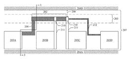
- FIG. 2 which includes FIGS. 2A and 2B , shows a top sectional view of an embodiment PCM structure and contact pads located in a horizontal separating region 207 of a wafer.
- FIG. 2A shows the wafer before singulation
- FIG. 2B shows a single die of the wafer after singulation.
- an embodiment PCM structure 202 includes a polysilicon resistor near the top surface of a wafer in a horizontal singulation lane 203 between two semiconductor circuit regions 204 A-B.
- Contact pads 205 A-D are electrically coupled to the PCM structure 202 by a polysilicon path 208 , metal traces 211 , and a silicon path 212 forming electrical paths.
- the PCM structure 202 is also electrically coupled to semiconductor circuit region 204 B via an electrical path 206 that is embedded below the wafer surface.
- a PCM structure may be coupled to a semiconductor circuit region by a surface path.
- a single PCM structure may be coupled to multiple semiconductor circuit regions.
- Contact pad 205 A is electrically coupled to the PCM structure 202 by a polysilicon path 208 .
- Polysilicon provides an electrical path with a higher resistance than a metallic conductor, but beneficially reduces the metal content of the singulation lane 203 .
- Such polysilicon connections may be used in embodiment applications where the PCM measurements have higher contact resistance tolerances.
- a metallic conductor coupled to a PCM structure may also be used for sensitive measurements, for example, sensitive resistance measurements.
- the direct metal interconnects 210 are electrically coupled to the contact pads 205 B and 205 C using metal traces 211 .
- the metallic conductor is made as narrow as possible to reduce the metal content in the singulation region, while still being wide enough to not introduce excess resistance to the measurement.
- the metallic conductor is made of the same material as the contact pad.
- An electrical path from a contact pad to a PCM structure may also be made from the same material as the wafer substrate by providing isolation on either side of the semiconductor path using, for example, deep trench isolation.
- a silicon path 212 disposed in the wafer substrate electrically couples the contact pad 205 D to the PCM structure 202 .
- different electrical paths between the contact pads and the PCM structures are designed to be composed of different materials.
- wafer design 42% of these electrical paths are composed of metal, and the remaining 58% are composed of a semiconductor material, such as polysilicon or the same material as the wafer substrate.
- at least 50% of the electrical paths between the contact pads and the PCM structures are composed of a semiconductor material.
- at least 50% of the electrical paths between the contact pads and the PCM structures are composed of metal.
- FIG. 2B shows the die of FIG. 2A after singulation along the singulation lane 203 .
- Each of the contact pads 205 A-D of FIG. 2B has no connection to any semiconductor circuit region and has a conductive connection that ends at the singulated edge 214 of the die.
- contact pads 205 B-C each have a metal trace 211 that ends at the singulated edge 214 .
- Pad 205 A has a polysilicon path 208 that ends at the singulated edge 214 .
- Contact pad 205 D has a silicon connection 212 that ends at the singulated edge 214 .
- FIG. 3 shows a cross-section of the PCM structure 202 and contact pad 205 A of FIG. 2A , both of which lie in a horizontal separating region 207 between the two semiconductor circuit regions 204 A and 204 B.
- Each of the semiconductor circuit regions has a crack stop 302 near its edge.
- the contact pad 205 A contacts an underlying polysilicon region 303 , which is partially embedded in an insulating layer 304 and is above the remaining wafer layers 306 .
- a thin portion of the insulating layer 304 also covers the PCM structure 202 within the horizontal singulation lane 203 .
- a PCM structure is exposed to the top surface 308 and is not covered by any layers.
- a PCM is buried down to a depth of several microns.
- the horizontal singulation lane 203 is a three-dimensional region for singulating through the semiconductor wafer.
- the horizontal singulation lane 203 intersects the PCM structure 202 and also intersects the top surface 308 and the bottom surface 310 , but does not intersect the contact pad 205 A.
- FIG. 4 is a flow diagram illustrating an embodiment method for generating a layout design of a semiconductor wafer using, for example, a CAD software application.
- a combined design for a PCM structure and a conductive contact pad is received.
- the combined design may also include a list of sensitive devices that need to be connected only with metal lines.
- the design for the PCM structure is extracted from the combined design such that the extracted design for the PCM structure lacks metal structures wider than 20 ⁇ m.
- layout locations are selected for arrays of PCM structures arranged in accordance with the extracted design. These layout locations are selected such that the arrays of PCM structures are within the singulation lanes.
- layout locations for arrays of contact pads are selected such that singulating through the singulation lanes would not include singulating through the contact pads.
- Each PCM structure in arrays of PCM structures may be, for example, adjacent to at least one contact pad in the arrays of contact pads.
- the layout generator also receives the technology specification providing various rules that need to be taken into account while generating the layout.
- One of the rules in the technology specification may include the maximum total metal content allowable for a singulation lane to minimize cracks and other effects. Some embodiments may include a minimum total metal content so that sensitive components are connected with metal lines.
- the layout may design the contact pad to be contiguous with a metallization layer of the semiconductor wafer.
- Electrical connections are laid out to couple the PCM structures to the contact pads such that all external electrical connections to the PCM structures are made through the contact pads. These electrical connections may be designed from polysilicon, metal, or the material that makes up the semiconductor substrate, but the electrical connections use non-metallic interconnects as much as possible as allowed in the technology specification.
- layout locations for arrays of semiconductor circuitry are selected such that the arrays of semiconductor circuitry are separated by the singulation regions.
- the remainder of the layout for the semiconductor wafer is completed.
- FIG. 5 is a flow diagram illustrating an embodiment method for semiconductor fabrication.
- at least one reticle is generated in accordance with a layout design for a semiconductor wafer.
- a PCM structure is formed in accordance with the at least one reticle such that the PCM structure does not include metal structures wider than 20 ⁇ m and the PCM structure is intersected by a singulation lane.
- the PCM structure may be disposed between semiconductor circuit regions of the wafer, as an example.
- a conductive contact pad is formed in accordance with the at least one reticle such that the contact pad is not intersected by the singulation lane.
- the PCM structure and contact pad may be adjacent to each other, as an example.
- the contact pad may be formed from a metallization layer of the semiconductor wafer.
- an electrical path such as, for example, a polysilicon path, metal path, or a path made of the substrate material, is formed to electrically couple the PCM structure and the conductive contact pad.
- the semiconductor wafer is singulated through the PCM structure but not through the contact pad. This singulating the wafer into a plurality of dies may damage the PCM structure without damaging the contact pad.
- FIG. 6 shows a block diagram of a processing system that may be used for implementing the layout generation methods disclosed herein.
- Specific devices may utilize all of the components shown, or only a subset of the components, and levels of integration may vary from device to device.
- a device may contain multiple instances of a component, such as multiple processing units, processors, memories, transmitters, receivers, etc.
- the processing system comprises a computer workstation.
- the processing system may comprise a processing unit equipped with one or more input/output devices, such as a speaker, microphone, mouse, touchscreen, keypad, keyboard, printer, display, and the like.
- the processing unit may include a CPU, memory, a mass storage device, a video adapter, and an Input/Output (I/O) interface connected to a bus.
- I/O Input/Output
- multiple processing units in a single processing system or in multiple processing systems may form a distributed processing pool or distributed editing pool.
- the mass storage device may comprise any type of storage device configured to store data, programs, and other information and to make the data, programs, and other information accessible via the bus.
- the mass storage device may comprise, for example, one or more of a solid state drive, hard disk drive, a magnetic disk drive, an optical disk drive, or the like.
- Embodiment dual-region structures may be used, for example, to produce semiconductor chips by mechanical dicing without introducing significant cracks.
- the embodiment dual-region structures are used in a semiconductor wafer that is laser singulated to allow more uniform heating of the edge of the die due to reduced metal content in the singulation lane.
Landscapes
- Engineering & Computer Science (AREA)
- Physics & Mathematics (AREA)
- Theoretical Computer Science (AREA)
- Computer Hardware Design (AREA)
- Geometry (AREA)
- Evolutionary Computation (AREA)
- General Engineering & Computer Science (AREA)
- General Physics & Mathematics (AREA)
- Architecture (AREA)
- Semiconductor Integrated Circuits (AREA)
- Automation & Control Theory (AREA)
- Manufacturing & Machinery (AREA)
- Testing Or Measuring Of Semiconductors Or The Like (AREA)
- Chemical & Material Sciences (AREA)
- Materials Engineering (AREA)
- Internal Circuitry In Semiconductor Integrated Circuit Devices (AREA)
Abstract
A semiconductor die includes a semiconductor circuit disposed within or over a substrate. A conductive contact pad is disposed over the substrate outside the semiconductor circuit. A floating electrical path ends at a singulated edge of the die. The electrical path is electrically coupled to the conductive contact pad.
Description
This application is a divisional of U.S. application Ser. No. 14/660,753, filed on Mar. 17, 2015, which application is hereby incorporated herein by reference.
The present invention relates generally to a system and method for singulation of semiconductors, and, in particular embodiments, to a system and method for dual-region singulation.
Process Control Monitoring (PCM) structures are semiconductor monitoring structures that can be used prior to singulating a semiconductor wafer into individual die. Monitoring with PCM structures can help determine whether fabrication processes are within appropriate process windows or whether individual devices that make up an Integrated Circuit (IC) are within device specifications.
Existing PCM systems, however, present cost and performance disadvantages by placing PCM structures and their conductive contact pads in the same region. For example, in block PCM designs, a region of the wafer that would otherwise be used to form a semiconductor chip is used to form one or more PCM structures and contact pads thereby reducing the number of chips per wafer. For wafers with only a few large semiconductor chips, these block PCM designs sacrifice a large fraction of the productive part of the wafer. Thus, when large semiconductor chips are used, PCM structures and their contact pads are often placed within the lanes where the dies are singulated. Yet singulating through metal pads can introduce imperfections that reduce production yield and create reliability problems for the semiconductor chips that are produced. For example, when mechanical sawing is used to singulate the die, vibrations introduced through the combination of metallic and non-metallic materials that differ in hardness can cause cracks, cavities, or other forms of surface and/or sidewall damage. Furthermore, because metallic and non-metallic materials exhibit different thermal behavior, singulating with a laser introduces material stresses due to dissimilar heating.
In accordance with an embodiment of the present invention, a semiconductor die is provided. The semiconductor die includes a semiconductor circuit, a conductive contact pad, and a floating electrical path ending at a singulated edge of the die, wherein the electrical path is electrically coupled to the conductive contact pad.
In accordance with another embodiment of the present invention, a method for semiconductor fabrication is provided. The method includes forming a first array of semiconductor circuitry and a second array of semiconductor circuitry separated by a singulation region and a contact region. The method also includes forming a first array of PCM structures within the singulation region of a substrate. The method also includes forming a first array of contact pads disposed in the contact region. The method also includes forming electrical connections between the first array of PCM structures and the first array of contact pads, wherein all external electrical connections to the first array of PCM structures are made through the first array of contact pads.
In accordance with another embodiment of the present invention, another method for semiconductor fabrication is provided. The method includes forming a PCM structure in a semiconductor wafer comprising a complete set of singulation regions for singulating through the semiconductor wafer, wherein the PCM structure is disposed within the complete set. The method also includes forming a conductive contact pad in the semiconductor wafer, wherein the conductive contact pad is electrically coupled to the PCM structure, and the conductive contact pad is not disposed within the complete set. The method also includes singulating the semiconductor wafer only within the complete set of singulation regions.
In accordance with another embodiment of the present invention, a method for layout generation is provided. The method includes obtaining a layout location of a singulation region for singulating through a semiconductor wafer, wherein the layout location is included in a layout representing the semiconductor wafer. The method also includes obtaining a design for a PCM structure and selecting an arrangement for the layout. The arrangement includes a first array of PCM structures each arranged in accordance with the design for the PCM structure, wherein the first array of PCM structures is disposed within the singulation region. The arrangement also includes a first array of contact pads disposed in a contact region, a first array of semiconductor circuitry and a second array of semiconductor circuitry separated by the singulation region and the contact region, and electrical connections between the first array of PCM structures and the first array of contact pads. All external electrical connections to the first array of PCM structures are made through the first array of contact pads.
For a more complete understanding of the present invention, and the advantages thereof, reference is now made to the following descriptions taken in conjunction with the accompanying drawings, in which:
The making and using of the presently preferred embodiments are discussed in detail below. It should be appreciated, however, that the present invention provides many applicable inventive concepts that can be embodied in a wide variety of specific contexts. The specific embodiments discussed are merely illustrative of specific ways to make and use the invention, and do not limit the scope of the invention. An exemplary wafer containing dies that are to be singulated through PCM structures will first be generally described in connection with FIG. 1 . More detail will then be provided for an embodiment in which a PCM structure and contact pads are located in a horizontal separating region of a wafer in connection with FIG. 2 . The cross-section of this horizontally-distributed PCM structure will be further explained in connection with FIG. 3 . A method for generating a layout design for a semiconductor wafer having PCM structures and contact pads will be discussed in connection with FIG. 4 . A method for fabricating the semiconductor wafer from the layout will be discussed in connection with FIG. 5 . Finally, a processing system used for implementing some of the embodiment devices and methods will be described in connection with FIG. 6 .
The present invention will be described with respect to embodiments in a specific context, a system and method for placing PCM structures and contact pads for use in monitoring particular features of a fabrication process, including physical characteristics such as line width, gate profile, contact opening, and other such as, for example, doping, resistance, capacitance, transistor performance, and others. Further embodiments may be applied to other PCM systems for measuring system and circuit level performance of one or more individual devices used to make up a complete semiconductor chip.
Referring now to FIG. 1A , a semiconductor wafer has semiconductor circuit regions 107, and these semiconductor circuit regions 107 are to be separated from each other by singulating through singulation lanes lying in separation regions between the semiconductor circuit regions 107. These singulation lanes are three-dimensional regions extending from the top to the bottom of the wafer. Singulation may be performed by, for example, mechanical sawing, laser cutting, or another separation technique. The embodiment semiconductor wafer of FIG. 1A has metal widths of less than or equal to 20 μm in the singulation lanes. Horizontal singulation lanes 102 lie in horizontal separation regions 103, and vertical singulation lanes 104 lie in wide vertical separation regions 105A and ordinary vertical separating regions 105B.
The semiconductor circuit regions 107 may include circuitry for, e.g., vertical power Metal Oxide Semiconductor Field-Effect Transistors (MOSFETs), other power transistors, or power chips; diodes; sensors; microprocessors or other integrated circuits including Very Large Scale Integration (VLSI), Small-Scale Integration (SSI), Medium-Scale Integration (MSI), or Ultra-Large-Scale Integration (ULSI) chips; bipolar transistors, or Insulated-Gate Bipolar Transistors (IGBTs).
The minima for the width L1 of the horizontal separating regions 103 and the width L3 of the ordinary vertical separating regions 105B are both dependent on manufacturing tolerances for singulation and in some embodiments these widths may be the same. The minimum for the width L2 of each wide vertical separating region 105A is increased to approximately twice the width L3 of an ordinary vertical separating region 105B to accommodate PCM regions 108 for locating PCM structures and pad regions 109 for locating contact pads. In some embodiments, L2 is less than twice L3 since singulation width tolerances can be at least partially integrated into the pad regions 109. In some embodiments, all vertical separating regions are widened to accommodate PCM regions 108 and pad regions 109 or to provide a constant stepping pitch to reduce complexity of equipment for singulating the wafer.
A lithographic process uses quartz plate reticles or photomasks to form the structures of the wafer. Although wafer structures formed by stepper lithography are depicted in FIG. 1A , other embodiments use mask aligner lithography in which a full wafer photomask forms an image on the entire wafer in a single exposure. In stepper lithography embodiments, a reticle will form an image on, for example, 1/100 or 1/50 of the wafer surface, and this pattern is a design repetition that is stepped across the wafer using a stepper. In the embodiment wafer of FIG. 1A , only eight such design repetitions 101 appear, and only eight semiconductor circuit regions 107 appear in each design repetition 101. In some embodiments the design repetition 101 can be stepped across the entire wafer over one hundred times and the semiconductor circuit region 107 can appear over one hundred times in each design repetition 101. In the embodiments of FIGS. 1A and 1B , fewer wide vertical separating regions 105A appear than semiconductor circuit regions 107 because the PCM regions 108 appear less frequently in each design repetition 101 than the semiconductor circuit regions 107. Other embodiment wafers have an equal number of widened separating regions and semiconductor circuit regions. A given wafer design may use a series of reticles to form different layers of the semiconductor circuit regions at different stages of the fabrication process. The layout of the reticles may be generated using, for example, Computer Aided Design (CAD).
In some embodiments, the layout will include multiple design repetitions with distinct arrangements of PCM structures, contact pads, electrical paths and interconnects. For example, a first arrangement may be laid out in a region of the semiconductor wafer that is to be singulated first, and a second distinct arrangement may be laid out in a region of the semiconductor wafer that is to be singulated later. In an embodiment, the first arrangement may be useful for mitigating formation of cracks that are more likely to form in regions that are to be singulated first. The first design may, for example, form PCM structures and contact pads in a first arrangement that optimally mitigates crack formation, for example, by using a lower metal content in the vertical singulation lane 104. The second design may offer other advantages such as, for example, decreasing resistance by using more metal interconnects to electrically couple connections pads to PCM structures.
Referring now to FIG. 1B , a top sectional view shows an exemplary wafer section 100 of the semiconductor wafer that includes regions for implementing embodiment PCM structures 111. One of ordinary skill would recognize that PCM structures 111 may include a wide variety of structures used for PCM such as, for example, capacitors, resistors, contact resistance structures, diodes, MOSFETs, bipolar transistors, IGBTs, heaters, isolation check structures, reliability test structures, layer stack structures, etc. For wafer technologies based on silicon, silicon carbide, silicon germanium, carbon (including graphene) or similar semiconductor materials, the PCM structures may be made of any of the foregoing materials, or materials derived therefrom, e.g., oxides, nitrides, or imides of the foregoing materials, polycrystalline silicon, or other derivative dielectric materials. Other embodiments using wafer technologies based on III-V or II-VI compound semiconductor substrates could use PCM structures that are also based on one or more of the elements that make up the substrate. Such III-V and II-VI compound substrates may include, for example, gallium nitride, gallium arsenide, indium arsenide, gallium phosphide, indium phosphide, aluminum arsenide, aluminum nitride, cadmium sulfide, zinc sulfide, cadmium telluride, and zinc telluride. In still other embodiments, similar to the semiconductor circuit regions 107 being monitored the PCM structures could also contain small amounts of metal or metallic compounds (less than 5%) such as, e.g., aluminum, copper, titanium, tungsten, cobalt, platinum, palladium, molybdenum, nickel, vanadium, silver, gold, and metal silicides, metal nitrides and alloys of the foregoing metals. By contrast, as illustrated in FIG. 1B , the surface contact pads 106A and buried contact pads 106B could be made entirely of these metals and metallic compounds.
Referring again to FIG. 1B , the four quadrants of the exemplary wafer section 100 are four dies that are to be singulated, i.e., separated, at horizontal singulation lane 102 and vertical singulation lane 104 to produce four semiconductor chips. Each quadrant of the wafer section 100 contains a semiconductor circuit region 107 to be assembled into a packaged semiconductor product. Each semiconductor circuit region 107 contains an active region 114 and a seal-ring 110. The seal-ring no is part of the termination structure surrounding the active region 114 and protects the active region 114 from problems caused by, e.g., Electro-Static Discharge (ESD) and by damage from singulation, for example, from cracks caused by mechanical sawing. The seal-ring no may include a crack stop region 112 that includes a gap on the top insulating layer of the wafer and is designed to prevent any cracks or chips which form on the singulation surface from propagating into the active region 114. The seal-ring no may also include a moisture barrier to prevent moisture from entering into the active region 114.
Referring again to FIG. 1B , the wide vertical separating regions 105A of the wafer are widened to accommodate PCM structures in (which are present in PCM regions 108) along with surface contact pads 106A and buried contact pad 106B, which are present in distinct pad regions 109. Each pad region 109 may be adjacent to a PCM region 108, as an example. Surface contact pads 106A and buried contact pad 106B are used for connecting external monitoring devices to the PCM structures 111. In the embodiment wafer of FIG. 1B , any connections to buried contact pad 106B are performed in a step prior to its burial beneath the wafer surface, while connections to surface contact pads 106A may still be performed since these pads are never buried. Surface contact pads 106A and buried contact pad 106B are made of electrically conductive material.
External monitoring devices can monitor the PCM structures 111 by connecting to the surface contact pads 106A (and buried contact pad 106B prior to burial) using, for example, conductive probe needles. In an embodiment, the surface contact pads 106A and buried contact pad 106B are made of the same metallic layer that will be used after singulation to make power metal bond connections to the top surface of each die from, for example, a bond wire of a sealed package containing the singulated die. In some embodiments, the contact pads have dimensions of the order of 50 μmm×50 μm in order to enable consistent connection with the probe needles.
In the embodiment of FIG. 1B , the PCM regions 108 lie within a vertical singulation lane 104. Because the surface contact pads 106A and buried contact pad 106B are in a region that is separate from the vertical singulation lane 104, any metal structures present in the vertical singulation lane 104 have metal widths of less than or equal to 20 μm, which is less than the minimum width needed to enable consistent connection with a test probe. In some embodiments, any metal structures that are present in any of the horizontal or vertical singulation lanes and that are also electrically coupled to a PCM structure have metal widths that are narrower than the width of the tip of a test probe. By reducing the metal content of the vertical singulation lane 104, damage to the die during singulation is avoided. In other embodiments, PCM structures 111 are present in horizontal singulation lanes 102 that lack metal structures wider than 20 μm, or in both horizontal and vertical singulation lanes that each lack metal structures wider than 20 μm.
In the embodiment of FIG. 1B , placement of the PCM regions 108 within a vertical singulation lane 104 allows the PCM structures 111 to be destroyed during singulation, which prevents unauthorized connection to the PCM structures of finished products and reverse engineering of the fabrication process. In other embodiments, PCM regions 108 are located in a horizontal singulation lane to prevent reverse engineering. In still other embodiments for applications in which reverse engineering is less of a concern, the PCM region 108 is not within a horizontal singulation lane 102 or a vertical singulation lane 104.
The embodiment of FIG. 1B also contains a materials measurement block 116 in the vertical separating regions 105 that can be used for other aspects of process monitoring. In other embodiments, the separating region also contains alignment structures that allow a feature on one layer of the wafer to be aligned with a target structure being formed. The materials measurement block 116 of FIG. 1B may include an oxide measurement region that contains a block of oxide upon which a thickness measurement can be made using an interferometer. The materials measurement block 116 may also contain a doping measurement region for monitoring doping levels indicative of the various regions of the wafer, for example, using scanning capacitance measurement and destructive techniques including spreading resistance measurement, secondary ion mass spectrometry, and others.
Referring now to FIG. 1C , in an alternative embodiment, wide horizontal separating regions 103A are widened relative to ordinary horizontal separating regions 103B to accommodate PCM regions 108 and pad regions 109 of an alternative design repetition 101B. The minimum for the width L4 of each wide horizontal separating region 103A is increased to approximately twice the width L1 of an ordinary horizontal separating region 103B to accommodate PCM regions 108 for locating PCM structures and pad regions 109 for locating contact pads. In some embodiments, L4 is less than twice L1 since singulation width tolerances can be at least partially integrated into the pad regions 109. In other embodiments, all horizontal separating regions are widened. The aspect ratio of the semiconductor circuit region may be a factor in selecting whether horizontal or vertical separating regions are widened. For example, in the embodiment of FIG. 1C , the top surface of semiconductor circuit region 107A has a greater vertical dimension than horizontal dimension.
Referring now to FIG. 1D , in a second alternative embodiment both wide vertical separation regions 105A and wide horizontal separating regions 103A are respectively widened relative to ordinary vertical separation regions 105B and ordinary horizontal separation regions 103B to accommodate PCM regions 108 and pad regions 109. In other embodiments, all horizontal separation regions are widened while only some vertical separation regions are widened, or vice versa.
Referring now to FIG. 1E , in a third alternative embodiment all vertical separating regions 105A and all horizontal separating regions 103A are respectively widened relative to ordinary vertical separation regions 105B and ordinary horizontal separation regions 103B (shown in FIG. 1D ) to accommodate PCM regions 108 and pad regions 109.
Referring now to FIG. 2A , an embodiment PCM structure 202 includes a polysilicon resistor near the top surface of a wafer in a horizontal singulation lane 203 between two semiconductor circuit regions 204A-B. Contact pads 205A-D are electrically coupled to the PCM structure 202 by a polysilicon path 208, metal traces 211, and a silicon path 212 forming electrical paths. The PCM structure 202 is also electrically coupled to semiconductor circuit region 204B via an electrical path 206 that is embedded below the wafer surface. In other embodiments, a PCM structure may be coupled to a semiconductor circuit region by a surface path. In still other embodiments, a single PCM structure may be coupled to multiple semiconductor circuit regions.
A metallic conductor coupled to a PCM structure may also be used for sensitive measurements, for example, sensitive resistance measurements. For instance, in the particular embodiment of FIG. 2A the direct metal interconnects 210 are electrically coupled to the contact pads 205B and 205C using metal traces 211. In an embodiment, the metallic conductor is made as narrow as possible to reduce the metal content in the singulation region, while still being wide enough to not introduce excess resistance to the measurement. In an embodiment, the metallic conductor is made of the same material as the contact pad.
An electrical path from a contact pad to a PCM structure may also be made from the same material as the wafer substrate by providing isolation on either side of the semiconductor path using, for example, deep trench isolation. For example, in the embodiment of FIG. 2A , a silicon path 212 disposed in the wafer substrate electrically couples the contact pad 205D to the PCM structure 202.
In some wafers, different electrical paths between the contact pads and the PCM structures are designed to be composed of different materials. For example, in one embodiment wafer design, 42% of these electrical paths are composed of metal, and the remaining 58% are composed of a semiconductor material, such as polysilicon or the same material as the wafer substrate. In various embodiments, at least 50% of the electrical paths between the contact pads and the PCM structures are composed of a semiconductor material. In still other embodiments, at least 50% of the electrical paths between the contact pads and the PCM structures are composed of metal.
The mass storage device may comprise any type of storage device configured to store data, programs, and other information and to make the data, programs, and other information accessible via the bus. The mass storage device may comprise, for example, one or more of a solid state drive, hard disk drive, a magnetic disk drive, an optical disk drive, or the like.
Illustrative embodiments of the present invention have the advantage of providing increased reliability without increasing costs significantly. Embodiment dual-region structures may be used, for example, to produce semiconductor chips by mechanical dicing without introducing significant cracks. In some embodiments, the embodiment dual-region structures are used in a semiconductor wafer that is laser singulated to allow more uniform heating of the edge of the die due to reduced metal content in the singulation lane.
While this invention has been described with reference to illustrative embodiments, this description is not intended to be construed in a limiting sense. Various modifications and combinations of the illustrative embodiments, as well as other embodiments of the invention, will be apparent to persons skilled in the art upon reference to the description. It is therefore intended that the appended claims encompass any such modifications or embodiments.
Claims (19)
1. A semiconductor die comprising:
a semiconductor circuit disposed within or over a substrate;
a conductive contact pad disposed over the substrate outside the semiconductor circuit; and
a electrical path ending at a singulated edge of the die, wherein the electrical path is electrically coupled to the conductive contact pad without being electrically coupled to the semiconductor circuit.
2. The semiconductor die of claim 1 , wherein the electrical path comprises a polysilicon path.
3. The semiconductor die of claim 1 , wherein the electrical path comprises a substrate material of the semiconductor circuit.
4. The semiconductor die of claim 1 , wherein the electrical path comprises aluminum, copper, titanium, tungsten, cobalt, platinum, palladium, molybdenum, nickel, vanadium, silver, gold, aluminum, a metal silicide, or a metal nitride.
5. The semiconductor die of claim 1 , wherein the conductive contact pad comprises aluminum, copper, titanium, tungsten, cobalt, platinum, palladium, molybdenum, nickel, vanadium, silver, gold, aluminum, a metal silicide, or a metal nitride.
6. The semiconductor die of claim 1 , wherein the semiconductor circuit comprises a metal oxide semiconductor field-effect transistor (MOSFET), a bipolar transistor, an insulated-gate bipolar transistor (IGBT), a diode, a sensor, or an integrated circuit.
7. A semiconductor die comprising:
an active region comprising a semiconductor circuit disposed within or over a substrate;
a seal-ring surrounding the active region;
a pad region disposed on one side of the seal-ring outside the active region;
a plurality of conductive contact pads disposed in the pad region; and
a plurality of electrical paths ending at a singulated edge of the die, wherein each of the plurality of electrical paths extend from a contact pad of the plurality of conductive contact pads without being electrically coupled to the semiconductor circuit.
8. The semiconductor die of claim 7 , wherein the plurality of electrical paths comprises polysilicon wires.
9. The semiconductor die of claim 7 , wherein the plurality of electrical paths comprises a substrate material of the substrate.
10. The semiconductor die of claim 7 , wherein the plurality of electrical paths comprises aluminum, copper, titanium, tungsten, cobalt, platinum, palladium, molybdenum, nickel, vanadium, silver, gold, aluminum, a metal silicide, or a metal nitride.
11. The semiconductor die of claim 7 , wherein the plurality of conductive contact pads comprises aluminum, copper, titanium, tungsten, cobalt, platinum, palladium, molybdenum, nickel, vanadium, silver, gold, aluminum, a metal silicide, or a metal nitride.
12. The semiconductor die of claim 7 , wherein the semiconductor circuit comprises a metal oxide semiconductor field-effect transistor (MOSFET), a bipolar transistor, an insulated-gate bipolar transistor (IGBT), a diode, a sensor, or an integrated circuit.
13. The semiconductor die of claim 7 , wherein the plurality of conductive contact pads comprises surface contact pads and buried contact pad.
14. The semiconductor die of claim 7 , wherein the seal-ring comprises a crack stop region that includes a gap on an uppermost insulating layer of the substrate.
15. A semiconductor die comprising:
an active region comprising a semiconductor circuit disposed within or over a substrate;
a seal-ring surrounding the active region;
a first pad region disposed on a first side of the seal-ring outside the active region;
a second pad region disposed on a second side of the seal-ring outside the active region;
a first plurality of conductive contact pads disposed in the first pad region; and
a first plurality of electrical paths ending at a first edge of the semiconductor die, wherein each of the first plurality of electrical paths extend from a contact pad of the first plurality of conductive contact pads without being electrically coupled to the semiconductor circuit;
a second plurality of conductive contact pads disposed in the second pad region; and
a second plurality of electrical paths ending at a second edge of the semiconductor die, wherein each of the second plurality of electrical paths extend from a contact pad of the second plurality of conductive contact pads without being electrically coupled to the semiconductor circuit.
16. The semiconductor die of claim 15 , wherein the first side intersects with the second side.
17. The semiconductor die of claim 15 , wherein the first plurality of electrical paths extend in a first direction away from the first plurality of conductive contact pads, wherein the second plurality of electrical paths extend in a second direction away from the second plurality of conductive contact pads, and wherein the first direction is perpendicular to the second direction.
18. The semiconductor die of claim 15 , wherein the first and the second plurality of electrical paths comprises polysilicon wires.
19. The semiconductor die of claim 15 , wherein the first and the second plurality of electrical paths comprises silicon.
Priority Applications (1)
| Application Number | Priority Date | Filing Date | Title |
|---|---|---|---|
| US15/403,673 US10090215B2 (en) | 2015-03-17 | 2017-01-11 | System and method for dual-region singulation |
Applications Claiming Priority (2)
| Application Number | Priority Date | Filing Date | Title |
|---|---|---|---|
| US14/660,753 US9583406B2 (en) | 2015-03-17 | 2015-03-17 | System and method for dual-region singulation |
| US15/403,673 US10090215B2 (en) | 2015-03-17 | 2017-01-11 | System and method for dual-region singulation |
Related Parent Applications (1)
| Application Number | Title | Priority Date | Filing Date |
|---|---|---|---|
| US14/660,753 Division US9583406B2 (en) | 2015-03-17 | 2015-03-17 | System and method for dual-region singulation |
Publications (2)
| Publication Number | Publication Date |
|---|---|
| US20170125315A1 US20170125315A1 (en) | 2017-05-04 |
| US10090215B2 true US10090215B2 (en) | 2018-10-02 |
Family
ID=56853198
Family Applications (2)
| Application Number | Title | Priority Date | Filing Date |
|---|---|---|---|
| US14/660,753 Expired - Fee Related US9583406B2 (en) | 2015-03-17 | 2015-03-17 | System and method for dual-region singulation |
| US15/403,673 Active US10090215B2 (en) | 2015-03-17 | 2017-01-11 | System and method for dual-region singulation |
Family Applications Before (1)
| Application Number | Title | Priority Date | Filing Date |
|---|---|---|---|
| US14/660,753 Expired - Fee Related US9583406B2 (en) | 2015-03-17 | 2015-03-17 | System and method for dual-region singulation |
Country Status (3)
| Country | Link |
|---|---|
| US (2) | US9583406B2 (en) |
| CN (2) | CN105990179B (en) |
| DE (1) | DE102016104762A1 (en) |
Families Citing this family (5)
| Publication number | Priority date | Publication date | Assignee | Title |
|---|---|---|---|---|
| US9583406B2 (en) | 2015-03-17 | 2017-02-28 | Infineon Technologies Austria Ag | System and method for dual-region singulation |
| US10418312B2 (en) * | 2015-10-29 | 2019-09-17 | Intel Corporation | Guard ring design enabling in-line testing of silicon bridges for semiconductor packages |
| CN112750765A (en) * | 2019-10-30 | 2021-05-04 | 台湾积体电路制造股份有限公司 | Method for manufacturing semiconductor structure |
| CN112259515B (en) * | 2020-11-10 | 2024-08-20 | 杭州晶通科技有限公司 | Test piece and test method for optimizing fan-out package metal interconnection process |
| WO2022169407A1 (en) | 2021-02-05 | 2022-08-11 | Heraeus Materials Singapore Pte. Ltd. | Coated wire |
Citations (13)
| Publication number | Priority date | Publication date | Assignee | Title |
|---|---|---|---|---|
| US6175394B1 (en) * | 1996-12-03 | 2001-01-16 | Chung-Cheng Wu | Capacitively coupled field effect transistors for electrostatic discharge protection in flat panel displays |
| US20080017979A1 (en) * | 2006-07-19 | 2008-01-24 | Chia-Yuan Chang | Semiconductor structure having extra power/ground source connections and layout method thereof |
| JP2008060094A (en) | 2006-08-29 | 2008-03-13 | Matsushita Electric Ind Co Ltd | Semiconductor device and manufacturing method thereof |
| US20080277659A1 (en) | 2007-05-10 | 2008-11-13 | Shih-Hsun Hsu | Test structure for semiconductor chip |
| US20080297501A1 (en) * | 2000-10-20 | 2008-12-04 | Toshio Miyazawa | Active matrix display device |
| US20100164521A1 (en) | 2007-06-08 | 2010-07-01 | Taiwan Semiconductor Manufacturing Company, Ltd. | Parametric Testline with Increased Test Pattern Areas |
| CN102105982A (en) | 2008-05-30 | 2011-06-22 | 格罗方德半导体公司 | Semiconductor device comprising a chip internal electrical test structure allowing electrical measurements during the fabrication process |
| US20130221353A1 (en) | 2012-02-23 | 2013-08-29 | Taiwan Semiconductor Manufacturing Company, Ltd. | Methods and Apparatus for Testing Pads on Wafers |
| US20130240882A1 (en) | 2012-03-15 | 2013-09-19 | Infineon Technologies Ag | Die, wafer and method of processing a wafer |
| CN103579196A (en) | 2012-07-27 | 2014-02-12 | 英飞凌科技股份有限公司 | Wafers and chips comprising test structures |
| US20140167226A1 (en) | 2007-11-12 | 2014-06-19 | Infineon Technologies Ag | Wafer and a Method of Dicing a Wafer |
| US20140264767A1 (en) | 2013-03-14 | 2014-09-18 | Infineon Technologies Ag | Wafer, Integrated Circuit Chip and Method for Manufacturing an Integrated Circuit Chip |
| US20160276233A1 (en) | 2015-03-17 | 2016-09-22 | Infineon Technologies Austria Ag | System and Method for Dual-Region Singulation |
Family Cites Families (13)
| Publication number | Priority date | Publication date | Assignee | Title |
|---|---|---|---|---|
| US4954875A (en) * | 1986-07-17 | 1990-09-04 | Laser Dynamics, Inc. | Semiconductor wafer array with electrically conductive compliant material |
| US6538213B1 (en) * | 2000-02-18 | 2003-03-25 | International Business Machines Corporation | High density design for organic chip carriers |
| US7327148B2 (en) * | 2005-06-29 | 2008-02-05 | Agilent Technologies, Inc. | Method for using internal semiconductor junctions to aid in non-contact testing |
| JP2009510758A (en) * | 2005-09-29 | 2009-03-12 | エヌエックスピー ビー ヴィ | Semiconductor device having improved contact pads and method of manufacturing the same |
| JP4884077B2 (en) * | 2006-05-25 | 2012-02-22 | ルネサスエレクトロニクス株式会社 | Semiconductor device |
| KR100831269B1 (en) * | 2006-12-29 | 2008-05-22 | 동부일렉트로닉스 주식회사 | Device for protecting semiconductor integrated circuit device from electrostatic discharge |
| US20090166843A1 (en) * | 2007-12-27 | 2009-07-02 | Infineon Technologies Ag | Semiconductor device and method for manufacturing a semiconductor device |
| CN102130025B (en) * | 2009-11-16 | 2015-03-11 | 三星电子株式会社 | Wafer, processing method thereof and method for manufacturing semiconductor device |
| IT1401220B1 (en) * | 2010-07-15 | 2013-07-12 | Metallux Sa | SENSOR AND MANUFACTURING METHOD. |
| JP5868043B2 (en) * | 2011-07-04 | 2016-02-24 | ルネサスエレクトロニクス株式会社 | Semiconductor device |
| ITTO20120515A1 (en) * | 2012-06-14 | 2013-12-15 | St Microelectronics Nv | ASSEMBLY OF AN INTEGRATED DEVICE TO SEMICONDUCTORS AND ITS MANUFACTURING PROCEDURE |
| US9165878B2 (en) * | 2013-03-14 | 2015-10-20 | United Test And Assembly Center Ltd. | Semiconductor packages and methods of packaging semiconductor devices |
| US8980714B2 (en) * | 2013-07-03 | 2015-03-17 | Infineon Technologies Dresden Gmbh | Semiconductor device with buried gate electrode structures |
-
2015
- 2015-03-17 US US14/660,753 patent/US9583406B2/en not_active Expired - Fee Related
-
2016
- 2016-03-15 DE DE102016104762.7A patent/DE102016104762A1/en active Pending
- 2016-03-16 CN CN201610150741.7A patent/CN105990179B/en active Active
- 2016-03-16 CN CN201811423613.0A patent/CN110008490B/en active Active
-
2017
- 2017-01-11 US US15/403,673 patent/US10090215B2/en active Active
Patent Citations (13)
| Publication number | Priority date | Publication date | Assignee | Title |
|---|---|---|---|---|
| US6175394B1 (en) * | 1996-12-03 | 2001-01-16 | Chung-Cheng Wu | Capacitively coupled field effect transistors for electrostatic discharge protection in flat panel displays |
| US20080297501A1 (en) * | 2000-10-20 | 2008-12-04 | Toshio Miyazawa | Active matrix display device |
| US20080017979A1 (en) * | 2006-07-19 | 2008-01-24 | Chia-Yuan Chang | Semiconductor structure having extra power/ground source connections and layout method thereof |
| JP2008060094A (en) | 2006-08-29 | 2008-03-13 | Matsushita Electric Ind Co Ltd | Semiconductor device and manufacturing method thereof |
| US20080277659A1 (en) | 2007-05-10 | 2008-11-13 | Shih-Hsun Hsu | Test structure for semiconductor chip |
| US20100164521A1 (en) | 2007-06-08 | 2010-07-01 | Taiwan Semiconductor Manufacturing Company, Ltd. | Parametric Testline with Increased Test Pattern Areas |
| US20140167226A1 (en) | 2007-11-12 | 2014-06-19 | Infineon Technologies Ag | Wafer and a Method of Dicing a Wafer |
| CN102105982A (en) | 2008-05-30 | 2011-06-22 | 格罗方德半导体公司 | Semiconductor device comprising a chip internal electrical test structure allowing electrical measurements during the fabrication process |
| US20130221353A1 (en) | 2012-02-23 | 2013-08-29 | Taiwan Semiconductor Manufacturing Company, Ltd. | Methods and Apparatus for Testing Pads on Wafers |
| US20130240882A1 (en) | 2012-03-15 | 2013-09-19 | Infineon Technologies Ag | Die, wafer and method of processing a wafer |
| CN103579196A (en) | 2012-07-27 | 2014-02-12 | 英飞凌科技股份有限公司 | Wafers and chips comprising test structures |
| US20140264767A1 (en) | 2013-03-14 | 2014-09-18 | Infineon Technologies Ag | Wafer, Integrated Circuit Chip and Method for Manufacturing an Integrated Circuit Chip |
| US20160276233A1 (en) | 2015-03-17 | 2016-09-22 | Infineon Technologies Austria Ag | System and Method for Dual-Region Singulation |
Also Published As
| Publication number | Publication date |
|---|---|
| CN105990179B (en) | 2018-12-21 |
| CN110008490B (en) | 2022-11-25 |
| US20160276233A1 (en) | 2016-09-22 |
| DE102016104762A1 (en) | 2016-09-22 |
| CN105990179A (en) | 2016-10-05 |
| CN110008490A (en) | 2019-07-12 |
| US9583406B2 (en) | 2017-02-28 |
| US20170125315A1 (en) | 2017-05-04 |
Similar Documents
| Publication | Publication Date | Title |
|---|---|---|
| US10090215B2 (en) | System and method for dual-region singulation | |
| KR101651047B1 (en) | Latch-up suppression and substrate noise coupling reduction through a substrate back-tie for 3d integrated circuits | |
| CN100561693C (en) | Method for providing structural support for interconnect pads while allowing signal conduction | |
| US20140339703A1 (en) | Structure and method for making crack stop for 3d integrated circuits | |
| US20080277659A1 (en) | Test structure for semiconductor chip | |
| CN102569238B (en) | Semiconductor device and manufacturing method thereof | |
| US20140077383A1 (en) | Structure and method of making an offset-trench crackstop that forms an air gap adjacent to a passivated metal crackstop | |
| US9401343B2 (en) | Method of processing a semiconductor wafer | |
| CN101150094A (en) | semiconductor wafer structure | |
| US20090140393A1 (en) | Wafer scribe line structure for improving ic reliability | |
| JP2012501077A (en) | A semiconductor device including a stress relaxation gap to enhance chip-package interaction stability. | |
| US20200303268A1 (en) | Semiconductor device including residual test pattern | |
| CN106960869B (en) | Wafer and forming method thereof | |
| US7314811B2 (en) | Method to make corner cross-grid structures in copper metallization | |
| TW202139351A (en) | Chip corner areas with a dummy fill pattern | |
| US20250355041A1 (en) | Interconnect structures in integrated circuit chips | |
| US10170439B1 (en) | Chamfering for stress reduction on passivation layer | |
| CN106206557A (en) | Silicon Interposer | |
| JP2003218114A (en) | Semiconductor device and manufacturing method thereof | |
| US12610854B2 (en) | Semiconductor device structure with bonding pad and method for forming the same | |
| US20240243077A1 (en) | Apparatus including air gap in scribe region of semiconductor device | |
| US20250006590A1 (en) | Double-sided integrated circuit with stabilizing cage | |
| US20250006663A1 (en) | Double-sided integrated circuit with electrostatic guard ring | |
| US20250006664A1 (en) | Three dimensional mechanically bolting staple fill | |
| TW202546444A (en) | Test element group and using the same |
Legal Events
| Date | Code | Title | Description |
|---|---|---|---|
| STCF | Information on status: patent grant |
Free format text: PATENTED CASE |
|
| MAFP | Maintenance fee payment |
Free format text: PAYMENT OF MAINTENANCE FEE, 4TH YEAR, LARGE ENTITY (ORIGINAL EVENT CODE: M1551); ENTITY STATUS OF PATENT OWNER: LARGE ENTITY Year of fee payment: 4 |
|
| MAFP | Maintenance fee payment |
Free format text: PAYMENT OF MAINTENANCE FEE, 8TH YEAR, LARGE ENTITY (ORIGINAL EVENT CODE: M1552); ENTITY STATUS OF PATENT OWNER: LARGE ENTITY Year of fee payment: 8 |