US10090048B2 - Semiconductor memory devices including a memory array and related method incorporating different biasing schemes - Google Patents
Semiconductor memory devices including a memory array and related method incorporating different biasing schemes Download PDFInfo
- Publication number
- US10090048B2 US10090048B2 US15/655,554 US201715655554A US10090048B2 US 10090048 B2 US10090048 B2 US 10090048B2 US 201715655554 A US201715655554 A US 201715655554A US 10090048 B2 US10090048 B2 US 10090048B2
- Authority
- US
- United States
- Prior art keywords
- address lines
- voltages
- combination
- column address
- row address
- Prior art date
- Legal status (The legal status is an assumption and is not a legal conclusion. Google has not performed a legal analysis and makes no representation as to the accuracy of the status listed.)
- Active
Links
- 230000015654 memory Effects 0.000 title claims abstract description 172
- 238000000034 method Methods 0.000 title claims abstract description 13
- 239000004065 semiconductor Substances 0.000 title claims description 20
- 239000000463 material Substances 0.000 description 30
- 239000004020 conductor Substances 0.000 description 19
- 230000005291 magnetic effect Effects 0.000 description 5
- 150000004770 chalcogenides Chemical class 0.000 description 3
- 238000010586 diagram Methods 0.000 description 2
- 229910000473 manganese(VI) oxide Inorganic materials 0.000 description 2
- 229910044991 metal oxide Inorganic materials 0.000 description 2
- 150000004706 metal oxides Chemical class 0.000 description 2
- ZKATWMILCYLAPD-UHFFFAOYSA-N niobium pentoxide Chemical compound O=[Nb](=O)O[Nb](=O)=O ZKATWMILCYLAPD-UHFFFAOYSA-N 0.000 description 2
- 229920000642 polymer Polymers 0.000 description 2
- 239000002861 polymer material Substances 0.000 description 2
- -1 silicon oxide nitride Chemical class 0.000 description 2
- HZNVUJQVZSTENZ-UHFFFAOYSA-N 2,3-dichloro-5,6-dicyano-1,4-benzoquinone Chemical compound ClC1=C(Cl)C(=O)C(C#N)=C(C#N)C1=O HZNVUJQVZSTENZ-UHFFFAOYSA-N 0.000 description 1
- SNLFYGIUTYKKOE-UHFFFAOYSA-N 4-n,4-n-bis(4-aminophenyl)benzene-1,4-diamine Chemical compound C1=CC(N)=CC=C1N(C=1C=CC(N)=CC=1)C1=CC=C(N)C=C1 SNLFYGIUTYKKOE-UHFFFAOYSA-N 0.000 description 1
- 229910016411 CuxO Inorganic materials 0.000 description 1
- 229910005866 GeSe Inorganic materials 0.000 description 1
- 229910005933 Ge—P Inorganic materials 0.000 description 1
- 229910005855 NiOx Inorganic materials 0.000 description 1
- 229910017629 Sb2Te3 Inorganic materials 0.000 description 1
- 229910002370 SrTiO3 Inorganic materials 0.000 description 1
- 229910010252 TiO3 Inorganic materials 0.000 description 1
- 229910003087 TiOx Inorganic materials 0.000 description 1
- 229910003134 ZrOx Inorganic materials 0.000 description 1
- 238000007792 addition Methods 0.000 description 1
- PNEYBMLMFCGWSK-UHFFFAOYSA-N aluminium oxide Inorganic materials [O-2].[O-2].[O-2].[Al+3].[Al+3] PNEYBMLMFCGWSK-UHFFFAOYSA-N 0.000 description 1
- 230000003321 amplification Effects 0.000 description 1
- 229910002113 barium titanate Inorganic materials 0.000 description 1
- 239000004106 carminic acid Substances 0.000 description 1
- 238000010276 construction Methods 0.000 description 1
- 229910052593 corundum Inorganic materials 0.000 description 1
- 238000013500 data storage Methods 0.000 description 1
- 238000012217 deletion Methods 0.000 description 1
- 230000037430 deletion Effects 0.000 description 1
- 230000001419 dependent effect Effects 0.000 description 1
- 230000005294 ferromagnetic effect Effects 0.000 description 1
- GNBHRKFJIUUOQI-UHFFFAOYSA-N fluorescein Chemical compound O1C(=O)C2=CC=CC=C2C21C1=CC=C(O)C=C1OC1=CC(O)=CC=C21 GNBHRKFJIUUOQI-UHFFFAOYSA-N 0.000 description 1
- 230000006870 function Effects 0.000 description 1
- 230000007274 generation of a signal involved in cell-cell signaling Effects 0.000 description 1
- 230000005415 magnetization Effects 0.000 description 1
- 238000012986 modification Methods 0.000 description 1
- 230000004048 modification Effects 0.000 description 1
- 238000003199 nucleic acid amplification method Methods 0.000 description 1
- 229910052814 silicon oxide Inorganic materials 0.000 description 1
- 229910052709 silver Inorganic materials 0.000 description 1
- 229910014031 strontium zirconium oxide Inorganic materials 0.000 description 1
- 239000004173 sunset yellow FCF Substances 0.000 description 1
- PBCFLUZVCVVTBY-UHFFFAOYSA-N tantalum pentoxide Inorganic materials O=[Ta](=O)O[Ta](=O)=O PBCFLUZVCVVTBY-UHFFFAOYSA-N 0.000 description 1
- HLLICFJUWSZHRJ-UHFFFAOYSA-N tioxidazole Chemical compound CCCOC1=CC=C2N=C(NC(=O)OC)SC2=C1 HLLICFJUWSZHRJ-UHFFFAOYSA-N 0.000 description 1
- 229910001845 yogo sapphire Inorganic materials 0.000 description 1
Images


Classifications
-
- G—PHYSICS
- G11—INFORMATION STORAGE
- G11C—STATIC STORES
- G11C13/00—Digital stores characterised by the use of storage elements not covered by groups G11C11/00, G11C23/00, or G11C25/00
- G11C13/0002—Digital stores characterised by the use of storage elements not covered by groups G11C11/00, G11C23/00, or G11C25/00 using resistive RAM [RRAM] elements
- G11C13/0021—Auxiliary circuits
- G11C13/0069—Writing or programming circuits or methods
-
- G—PHYSICS
- G11—INFORMATION STORAGE
- G11C—STATIC STORES
- G11C11/00—Digital stores characterised by the use of particular electric or magnetic storage elements; Storage elements therefor
- G11C11/02—Digital stores characterised by the use of particular electric or magnetic storage elements; Storage elements therefor using magnetic elements
- G11C11/16—Digital stores characterised by the use of particular electric or magnetic storage elements; Storage elements therefor using magnetic elements using elements in which the storage effect is based on magnetic spin effect
- G11C11/165—Auxiliary circuits
- G11C11/1659—Cell access
-
- G—PHYSICS
- G11—INFORMATION STORAGE
- G11C—STATIC STORES
- G11C11/00—Digital stores characterised by the use of particular electric or magnetic storage elements; Storage elements therefor
- G11C11/02—Digital stores characterised by the use of particular electric or magnetic storage elements; Storage elements therefor using magnetic elements
- G11C11/16—Digital stores characterised by the use of particular electric or magnetic storage elements; Storage elements therefor using magnetic elements using elements in which the storage effect is based on magnetic spin effect
- G11C11/165—Auxiliary circuits
- G11C11/1673—Reading or sensing circuits or methods
-
- G—PHYSICS
- G11—INFORMATION STORAGE
- G11C—STATIC STORES
- G11C11/00—Digital stores characterised by the use of particular electric or magnetic storage elements; Storage elements therefor
- G11C11/02—Digital stores characterised by the use of particular electric or magnetic storage elements; Storage elements therefor using magnetic elements
- G11C11/16—Digital stores characterised by the use of particular electric or magnetic storage elements; Storage elements therefor using magnetic elements using elements in which the storage effect is based on magnetic spin effect
- G11C11/165—Auxiliary circuits
- G11C11/1675—Writing or programming circuits or methods
-
- G—PHYSICS
- G11—INFORMATION STORAGE
- G11C—STATIC STORES
- G11C13/00—Digital stores characterised by the use of storage elements not covered by groups G11C11/00, G11C23/00, or G11C25/00
- G11C13/0002—Digital stores characterised by the use of storage elements not covered by groups G11C11/00, G11C23/00, or G11C25/00 using resistive RAM [RRAM] elements
- G11C13/0004—Digital stores characterised by the use of storage elements not covered by groups G11C11/00, G11C23/00, or G11C25/00 using resistive RAM [RRAM] elements comprising amorphous/crystalline phase transition cells
-
- G—PHYSICS
- G11—INFORMATION STORAGE
- G11C—STATIC STORES
- G11C13/00—Digital stores characterised by the use of storage elements not covered by groups G11C11/00, G11C23/00, or G11C25/00
- G11C13/0002—Digital stores characterised by the use of storage elements not covered by groups G11C11/00, G11C23/00, or G11C25/00 using resistive RAM [RRAM] elements
- G11C13/0007—Digital stores characterised by the use of storage elements not covered by groups G11C11/00, G11C23/00, or G11C25/00 using resistive RAM [RRAM] elements comprising metal oxide memory material, e.g. perovskites
-
- G—PHYSICS
- G11—INFORMATION STORAGE
- G11C—STATIC STORES
- G11C13/00—Digital stores characterised by the use of storage elements not covered by groups G11C11/00, G11C23/00, or G11C25/00
- G11C13/0002—Digital stores characterised by the use of storage elements not covered by groups G11C11/00, G11C23/00, or G11C25/00 using resistive RAM [RRAM] elements
- G11C13/0021—Auxiliary circuits
- G11C13/0023—Address circuits or decoders
-
- G—PHYSICS
- G11—INFORMATION STORAGE
- G11C—STATIC STORES
- G11C13/00—Digital stores characterised by the use of storage elements not covered by groups G11C11/00, G11C23/00, or G11C25/00
- G11C13/0002—Digital stores characterised by the use of storage elements not covered by groups G11C11/00, G11C23/00, or G11C25/00 using resistive RAM [RRAM] elements
- G11C13/0021—Auxiliary circuits
- G11C13/003—Cell access
-
- G—PHYSICS
- G11—INFORMATION STORAGE
- G11C—STATIC STORES
- G11C13/00—Digital stores characterised by the use of storage elements not covered by groups G11C11/00, G11C23/00, or G11C25/00
- G11C13/0002—Digital stores characterised by the use of storage elements not covered by groups G11C11/00, G11C23/00, or G11C25/00 using resistive RAM [RRAM] elements
- G11C13/0021—Auxiliary circuits
- G11C13/004—Reading or sensing circuits or methods
-
- G—PHYSICS
- G11—INFORMATION STORAGE
- G11C—STATIC STORES
- G11C5/00—Details of stores covered by group G11C11/00
- G11C5/02—Disposition of storage elements, e.g. in the form of a matrix array
-
- G—PHYSICS
- G11—INFORMATION STORAGE
- G11C—STATIC STORES
- G11C8/00—Arrangements for selecting an address in a digital store
- G11C8/10—Decoders
-
- G—PHYSICS
- G11—INFORMATION STORAGE
- G11C—STATIC STORES
- G11C13/00—Digital stores characterised by the use of storage elements not covered by groups G11C11/00, G11C23/00, or G11C25/00
- G11C13/0002—Digital stores characterised by the use of storage elements not covered by groups G11C11/00, G11C23/00, or G11C25/00 using resistive RAM [RRAM] elements
- G11C13/0021—Auxiliary circuits
- G11C13/004—Reading or sensing circuits or methods
- G11C2013/0054—Read is performed on a reference element, e.g. cell, and the reference sensed value is used to compare the sensed value of the selected cell
Definitions
- Embodiments of the present disclosure relate generally to non-volatile memory. More particularly, embodiments of the present disclosure are directed to methods of reading and writing memory devices as well as to such memory devices.
- Cross-point memories are memories that use intersecting address lines, such as row and column lines, with an intervening memory element.
- Examples of cross-point memories include magnetoresistive random access memory (MRAM), resistive random access memory (RRAM), ferroelectric random access memory (FRAM), silicon oxide nitride oxide semiconductor memory, polymer memory, and phase-change memory.
- the memory element for conventional cross-point memories may be programmed by varying the voltage across the memory element (e.g., phase-change memory), or by varying the polarity of the voltage across the memory element (e.g., MRAM and some RRAM).
- RRAM devices use resistive switching memory elements as an electronic memory.
- One type of RRAM memory element utilizes a material that may be, in one application, electrically switched between a first resistive value and a second resistive value based on the polarity of a current through the memory element. For example, a current pulsed though the memory element in a first polarity may cause the memory element to comprise a first resistive value representing a 1, while a current pulsed through the same memory element in a second, opposite polarity may cause the memory element to comprise a second resistive value representing a 0.
- MRAM devices store information as an orientation of a magnetization.
- One type of MRAM memory element utilizes a magnetic tunnel junction (MJT).
- An MJT is typically formed from two ferromagnetic plates, each of which is configured to hold a magnetic field, separated by a thin insulating layer.
- One of the two plates is typically a permanent magnet set to a particular polarity, and the other plate is typically configured with a magnetic field that will change polarity to match that of an external field.
- a memory element may be written by passing a current through wires placed just above and below the MTJ element.
- a current in one polarity results in a magnetic field of the other plate in a particular polarity, while a current in the opposite polarity results in a magnetic field of the other plate that is opposite to the particular polarity.
- FIG. 1 illustrates a block diagram of a memory device according to some embodiments.
- FIGS. 2A-2D illustrate a schematic depiction of at least one embodiment of at least a portion of a single plane in a memory array.
- FIGS. 3A and 3B are a schematic depiction of at least one embodiment of a portion of a single plane in a memory array.
- FIG. 4 is a schematic of a computing system diagram showing at least one semiconductor memory device containing at least one cross-point memory device according to at least one embodiment of the present disclosure.
- FIG. 5 is a truth table showing the various possible voltages to a memory element and respective selection device, as well as the written value according to at least one embodiment.
- a cross-point memory device 10 is depicted in accordance with at least one embodiment of the present disclosure.
- the memory device 10 may include cross-point memory 100 comprising a plurality of address lines extending in a first direction and a plurality of intersecting address lines (e.g., transverse).
- first address lines extend in a first direction (e.g., across the figure), and may be respectively illustrated and referred to herein as rows, or row address lines, extending across the page.
- second address lines extend in a second direction (into and out of the figure), across the first address lines, and may be respectively illustrated and referred to herein as columns, or column address lines.
- first (e.g., row) address lines may be second (e.g., column) address lines, and vice versa, depending on the orientation of the memory array.
- second (e.g., column) address lines may be provided according to various embodiments. Examples of such devices are described in U.S. Publication No. 2006/0120136, now U.S. Pat. No. 7,359,227, issued Apr. 15, 2008, as well as U.S.
- cross-point memory implemented as an RRAM device
- any other cross-point memory may be used in other embodiments of the present disclosure.
- the cross-point memory may be implemented as a MRAM, FRAM, PCRAM, or other memories that are known to those of ordinary skill in the art in which the memory cells may be configured into a cross-point array.
- pairs of adjacent, intersecting address lines define at least one cell between them (also referred to herein as a “memory cell”).
- Each cell may include a memory element 110 and a selection device 120 .
- a row address line e.g., Row 3 in FIGS. 2A-2D, 3A and 3B
- a column address line e.g., one of Col. 1 B, 2 B, 3 B, or 4 B in FIGS. 2A-3B
- is adjacent e.g., extends over) at least a portion of a second, opposing side of the cell.
- each row address line is electrically coupled to row decode/enable circuitry 130 that is configured to provide a respective voltage (including, e.g., a reference voltage, such as ground) to a plurality of row address lines in the array.
- each column address line is electrically coupled to column decode/enable circuitry 140 that is configured to provide similar respective voltages to each column address line in the array.
- the memory device 10 further includes an address buffer and signal generation circuit 150 , a write driver circuit 160 , a read amplification circuit 170 , a sense amplifier 180 and a data input/output buffer 190 .
- the data input/output buffer 190 is configured to provide write data values to the write driver circuitry 160 .
- a plurality of row address lines may be selected by the row decode/enable circuitry 130 , and the write driver circuitry 160 may apply one or more reset pulses or set pulses to the plurality of column address lines selected by the column decode/enable circuitry 140 .
- Various configurations for applying the one or more reset pulses or set pulses to the plurality of column address lines to store the plurality of data values in multiple memory cells are described in more detail below.
- the memory element 110 may comprise a resistive changing material suitable for non-volatile memory data storage.
- the resistive changing material may be a material having electrical properties (e.g., resistance) that may be changed through the application of energy such as, for example, heat, light, voltage potential, or electrical current.
- suitable resistive changing materials may include a phase-change or ionic conducting chalcogenide material, a binary metal oxide material, a perovskite oxide material, a colossal magnetoresistive material, or a polymer material.
- a phase-change chalcogenide material may comprise doped or undoped Ge 2 Sb 2 Te 5 or Sb 2 Te 3 .
- An ionic conducting chalcogenide material may comprise Ag-doped GeSe or GeS.
- a binary metal oxide material may comprise HfO x , Nb 2 O 5 , Al 2 O 3 , WO x , Ta 2 O 5 , TiO x , ZrO x , Cu x O or NiO x O.
- a perovskite oxide material may comprise doped or undoped SrTiO 3 , SrZrO 3 , or BaTiO 3 .
- a colossal magnetoresistive material may comprise Pr (1-x) Ca x MnO 3 (PCMO), La (1-x) Ca x MnO 3 (LCMO), or Ba (1-x) Sr x TiO 3 .
- a polymer material may comprise Alq 3 Ag, Cu-TCNQ, DDQ, TAPA, or a fluorescine-based polymer.
- the selection device 120 may comprise a material that does not change phase, but remains permanently amorphous and its current-voltage characteristics may remain at least substantially the same throughout its operating life.
- the selection device 120 may comprise As—Te—I, TiAs(Se, Te) 2 , Si—Te—As—Ge, Si—Te—As—Ge—P, Al—As—Te, Al—Ge—As—Te, Te 39 As 36 Si 17 Ge 7 P 1 , although the scope of embodiments of the present disclosure is not limited to just these materials.
- the selection device 120 may comprise a material that possesses bipolar rectification properties.
- a selection device 120 between the intersecting address lines turns on, allowing current flow across a memory element 110 .
- shared address lines are utilized. Namely, address lines can be shared between an overlying cell and an underlying cell. For example, with reference to FIG. 2A , column address line Col. 1 A is shared between overlying cells including the memory element 110 A and the selection device 120 A and underlying cells including the memory element 110 E and the selection device 120 E.
- the row address line Row 2 functions for selection of its overlying cells, including the memory elements 110 E- 110 H and the selection devices 120 E- 120 H, as well as for selection of its underlying cells, including the memory elements 110 I- 110 L and the selection devices 120 I- 120 L.
- a voltage biasing system is used such that address lines can be shared.
- a read or write voltage may be applied to one or more address lines.
- a read or write voltage may be applied to a row address line, such as Row 2 .
- One or more columns may be selected by providing a reference voltage, such as ground, on the appropriate column address lines.
- column address lines Col. 1 A and Col. 3 A, located above Row 2 , and Col. 1 B and Col. 2 B, located below Row 2 may be grounded (e.g., by biasing those lines to 0V).
- a read or write voltage may be applied to a column address line, such as column address lines Col. 4 A, Col.
- a row address line such as row address lines Row 1 and Row 3
- cells made up of the selection devices 120 D, 120 E, 120 G, 120 I, 120 J, 120 O and 120 P and the memory elements 110 D, 110 E, 110 G, 110 I, 110 J, 110 O and 110 P will be selected for reading or writing thereto.
- the memory element may be programmed into one of at least two memory states by applying an electrical signal to the memory material, the electrical signal having one of two opposing polarities referred to herein as positive or negative.
- a positive or negative electrical signal may change the resistance of the memory material between a relatively high resistance state and a relatively low resistance state.
- Programming of the memory element to change the resistance of the material may be accomplished by applying different voltages to respective crossing address lines, thereby generating a voltage potential across the memory material in a particular polarity.
- the information stored in the memory elements 110 may be read by measuring the resistance of the memory material.
- a read current may be provided to the memory material using crossing address lines, such as Row 1 and Col. 1 A, and a resulting read voltage across the memory material may be compared against a reference voltage using, for example, a sense amplifier (not shown).
- the read voltage may be proportional to the resistance exhibited by the memory material.
- the selection device 120 is off and may exhibit very high resistance in some embodiments.
- the off resistance can, for example, range from 50,000 ohms to greater than 10 gigaohms at a bias of half the threshold voltage.
- the selection devices 120 may remain in the off state until a threshold voltage or threshold current switches the selection device 120 to a highly conductive, low resistance on state.
- the voltage across the selection device 120 after it is turned on may drop to a slightly lower voltage, called the holding voltage and may remain very close to this holding voltage.
- the threshold voltage may be on the order of about 1.1 volts and the holding voltage may be on the order of about 0.9 volt.
- the selection device 120 voltage drop remains close to the holding voltage as the current passing through the device is increased up to a certain, relatively high, current level. Above that current level the device remains on but displays a finite differential resistance with the voltage drop increasing with increasing current.
- the selection device 120 may remain on until the current through the selection device 120 is dropped below a characteristic holding current value that is dependent on the area of the material and may be impacted by top and bottom electrodes utilized to form the selection device 120 .
- the memory elements 110 may be configured to store a 1 when a voltage across a respective memory element 110 and selection device 120 is positive voltage V 0 , and to store a 0 when the voltage across a respective memory element 110 and selection device 120 is a negative voltage ⁇ V 0 .
- voltage V 0 comprises a voltage sufficient to switch the selection device 120 to the on state and to change the resistance of the memory element 110 .
- the memory elements 110 and selection devices 120 are configured such that a positive voltage V 0 alters the memory element 110 to a high resistance, while a negative voltage ⁇ V 0 alters the memory element 110 to a low resistance.
- embodiments described herein with reference to FIGS. 2A-3B also illustrate, by way of example and not limitation, embodiments wherein the voltage applied is considered positive when the upper conductor of a respective memory element 110 and section device 120 (as oriented in the FIGS.) is a higher voltage than the lower conductor, and negative when the lower conductor is a higher voltage than the upper conductor.
- FIG. 5 is a truth table showing the various possible voltages to a memory element 110 and respective selection device 120 , as well as the resulting change, if any, to the memory element 110 .
- a voltage of 0V is applied to both the upper conductor (referred to as “top” in FIG. 5 ) and the lower conductor (referred to as “bottom” in FIG. 5 )
- the voltage from top to bottom is 0V and nothing is written to the respective memory element 110 .
- the voltage at the upper conductor is 0V and the voltage at the lower conductor is 1 ⁇ 2V 0
- the voltage from top to bottom is ⁇ 1 ⁇ 2 V 0 and nothing is written to the respective memory element 110 .
- a 1 may be written to each memory element 110 I and 110 J in the embodiment illustrated in FIG. 2A when the row address line Row 2 is biased at voltage V 0 and the column address lines Col. 1 B and Col. 2 B are grounded.
- a 1 may be written to each memory element 110 O and 110 P when the row address line Row 3 is grounded and the column address lines Col. 3 B and Col. 4 B are biased at voltage V 0 .
- the memory elements 110 may be configured to store a 0 when a voltage across a respective memory element and selection device is ⁇ V 0 .
- row address line Row 1 or Row 3 may be grounded.
- One or more columns may be selected by applying a voltage V 0 to the appropriate column address line.
- a voltage V 0 may be applied to the column address lines Col. 1 A, Col. 3 A and Col. 4 A.
- cells made up of the selection devices 120 D, 120 E and 120 G and the memory elements 110 D, 110 E and 110 G will be selected with a ⁇ V 0 , resulting in a 0 being written to each memory element 110 D, 110 E and 110 G.
- unselected address lines such as the column address line Col. 2 A
- unselected address lines may be biased at a voltage less than the read or write voltage and greater than the reference voltage.
- unselected address lines may be biased at half the write voltage (i.e., one-half V 0 ) such that the potential across cells of the unselected address lines (e.g., selection devices 120 B and 120 F and memory elements 110 B and 110 F in FIG. 2A ) is a positive or negative one-half V 0 .
- the potential across unselected cells is either zero (e.g., in the case of selection devices 120 A, 120 C, 120 H, etc., and memory elements 110 A, 110 C, 110 H, etc., in FIG.
- the selection devices may be configured such that the half voltage is insufficient to turn on the selection devices 120 resulting in no current flow or relatively low current flow across a cell
- the memory elements 110 may be configured such that the half voltage is insufficient to change the resistance of the memory element, or a combination thereof.
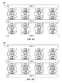
- FIG. 2A is a schematic depiction of at least one embodiment of at least a portion of a single plane in a memory array.
- a “single plane” in the memory array includes each of the first address lines extending parallel to each other and located in a common vertical plane of the memory array. For example, in the embodiment set forth in FIG.
- one or more of column address lines Col. 1 A through Col. 4 B may be selected and pulsed simultaneously with voltages of 0V or V 0 to write a 1 or 0 value to at least some of the memory elements 110 , as described herein above.
- a total of 7 bits are written in a single clock cycle.
- FIG. 2B illustrates the cross-point memory 100 of FIG. 2A after the memory elements 110 described above have been written. Subsequent to writing the memory elements 110 described above, it may be desired to write to memory elements 110 on the opposing side of at least some of the address lines. For example, it may be desired to write a 1 to memory element 110 L, as well as to write a 0 to memory elements 110 A and 110 H. Thus, as shown in FIG. 2B , a voltage V 0 may be applied to the column address line Col. 1 A, and the column address lines Col. 4 A and Col. 4 B may be grounded. In order to protect the remaining memory elements 110 , a voltage of one-half V 0 may be applied to column address lines Col. 2 A, Col. 3 A, Col. 1 B, Col. 2 B and Col. 3 B.
- FIG. 2C illustrates the cross-point memory 100 of FIGS. 2A and 2B after the memory elements 110 have been written as described with reference to FIG. 2B .
- the row address lines Row 1 -Row 3 may have opposite voltages applied thereto.
- row address lines Row 1 and Row 3 may have voltage V 0 applied thereto, while row address line Row 2 may be grounded.
- the voltage levels applied to column address lines Col. 1 A through Col. 4 B depends on the desired value written to the memory elements 110 not yet containing a value.
- a value of 1 might be desired to be written to memory elements 110 B and 110 C, and a value of 0 might be desired to be written to memory element 110 M, 110 N and 110 K.
- a voltage V 0 may be applied to the column address line Col. 3 B and column address lines Col. 2 A, Col. 3 A, Col. 1 B and Col. 2 B may be grounded.
- a voltage of one-half V 0 may be applied to column address lines Col. 1 A, Col. 4 A and Col. 4 B.
- the last remaining memory element 110 F may have a 1 written thereto, for example.
- a voltage V 0 may be applied to column address line Col. 2 A while a voltage of one-half V 0 may be applied to all the remaining column address lines Col. 1 A, Col. 3 A, Col. 4 A, Col. 1 B, Col. 2 B, Col. 3 B and Col. 4 B in order to protect the associated memory elements 110 .
- the entire page illustrated in FIGS. 2A-2D may be written to in just a few clock cycles.
- a cross-point memory 100 may be configured to read/write a full word in only two clock cycles.
- FIG. 3A illustrates an embodiment cross-point memory 100 configured to read/write a word comprising 8 bits.
- row address line Row 2 may have a voltage V 0 applied thereto while row address lines Row 1 and Row 3 may have a voltage one-half V 0 applied thereto.
- an eight-bit word comprises 00100110, a first plurality of data may be written at least substantially simultaneously and a second, remaining plurality of data may be written at least substantially simultaneously.
- each of memory elements 110 J and 110 K will have a value of 1 written thereto and each of memory elements 110 E, 110 F and 110 H will have a 0 written thereto.
- Each of the remaining column address lines Col. 3 A, Col. 1 B and Col. 4 B may have either a voltage V 0 applied thereto or a voltage one-half V 0 applied thereto to protect their corresponding memory elements 110 from being enabled.
- FIG. 3B illustrates the cross-point memory 100 of FIG. 3A subsequent to writing the first plurality of data as described above.
- Row address line Row 2 may be grounded while the one-half V 0 voltage is still applied to row address lines Row 1 and Row 3 .
- a voltage V 0 is applied to column address lines Col. 3 A, Col. 1 B and Col. 4 B.
- Each of the remaining column address lines Col. 1 A, Col. 2 A, Col. 4 A, Col. 2 B and Col. 3 B may either be grounded or have a voltage of one-half V 0 applied thereto to protect their corresponding memory elements 110 from being enabled.
- the example provided herein with reference to FIGS. 3A and 3B describe the column address lines being pulsed to write to respective memory elements 110 .
- the row address lines may be pulsed after a particular voltage is applied to the respective column address lines.
- the respective voltages may be applied to each of the column address lines.
- a voltage V 0 may be pulsed on row address line Row 2 followed by grounding the same row address line Row 2 . In such an embodiment, it may not be necessary to change the voltages applied to the column address lines.
- an 8-bit word may be written to a plurality of memory elements 110 in just a couple of clock cycles and in close proximity in the cross-point memory array.
- a system employing larger word sizes e.g., 16 bit, 32 bit, etc. may similarly be written such that at least one word may be read/written in a minimum number of clock cycles.
- an electronic system 400 such as a computer system, in accordance with an embodiment of the present disclosure, comprises at least one input device 410 , at least one output device 420 , at least one memory access device, such as processor 430 , and at least one memory device 440 .
- the term “computer system” includes not only computers, such as personal computers and servers, but also wireless communications devices (e.g., cell phones, personal digital assistants configured for text messaging and email), cameras, chip sets, set top boxes, controllers, vehicle and engine control and sensor systems, digital music players, and other combinations of the above-referenced input, output, processor and memory devices.
- the at least one memory device 440 comprises at least one cross-point memory device (e.g., device 100 ) comprising a plurality of memory cells having a memory element coupled to a selection device.
- Such methods may comprise biasing a plurality of first address lines and biasing a plurality of second address lines.
- Each first address line of the plurality may be adjacent a first side of some of a plurality of cells in a single plane of a three-dimensional array of cells.
- Each cell may comprise a memory element and a selection device.
- the plurality of second address lines may extend across the plurality of first address lines.
- Each second address line may extend over a second, opposing side of at least one cell of the plurality of cells in the single plane of the three-dimensional array of cells such that a plurality of cells in the single plane of the array of cells are accessed at least substantially simultaneously and at least one cell of the plurality of cells in the single plane is not accessed.
- methods of storing a plurality of data values into a selected portion of memory cells in a common plane of a three-dimensional memory array may comprise biasing at least one first address line extending in first direction. At least one side of each of a plurality of cells in the common plane may be adjacent to at least one of the first address lines, each cell comprising a memory element and a selection device. A plurality of second address lines extending across the at least one first address line may be biased. Each second address line may be adjacent a side of a cell of the plurality of cells opposite the side of the cell adjacent to a respective one of the at least one first address lines. At least some of the plurality of data values may be stored at least substantially simultaneously in at least some of the plurality of cells.
- methods of at least substantially simultaneously writing to a plurality of memory cells may comprise selectively applying a reference voltage to at least one first address line in a plane.
- Each of the at least one first address lines may be adjacent to a first side of some of a plurality of cells comprising a memory element and a selection device.
- a write voltage or a voltage less than the write voltage and greater than the reference voltage may be selectively applied to at least one other first address line located in the plane and adjacent to the at least one first address line.
- the write voltage or the reference voltage may be selectively applied to a plurality of second address lines extending across the at least one first address line.
- Each second address line of the plurality of second address lines may be adjacent to a second, opposing side of a respective cell of the plurality of cells.
- a memory device may comprise a plurality of cells, each cell comprising a memory element and a selection device.
- a plurality of first address lines may be adjacent a first side of at least some cells of the plurality of cells.
- a plurality of second address lines may extend across to the plurality of first address lines, and each second address line may be adjacent a second, opposing side of at least some cells of the plurality of cells.
- Control circuitry may be configured to selectively apply a write voltage or a reference voltage at least substantially simultaneously to the plurality of first address lines and to selectively apply a write voltage, a reference voltage, or a voltage less than the write voltage and greater than the reference voltage at least substantially simultaneously to the plurality of second address lines.
- an electronic system may comprise a memory access device and a memory device coupled thereto.
- the memory device may comprise a plurality of memory cells in a common plane. Each memory cell may comprise a memory element coupled to a selection device.
- a first address line of a plurality of first address lines may be adjacent a first side of at least some cells of the plurality of cells.
- a plurality of second address lines may extend across the plurality of first address lines. Each second address line may be adjacent a second, opposing side of at least some cells of the plurality of cells.
- a first decode/enable circuitry may be configured to selectively apply a write voltage or a reference voltage to the first address lines.
- a second decode/enable circuitry may be configured to selectively apply a write voltage, a reference voltage, or a voltage less than the write voltage and greater than the reference voltage to at least some of the plurality of second address lines such that at least some of the plurality of memory cells are accessed at least substantially simultaneously.
- the embodiments described herein are directed to cross-point memories configured for bipolar switching (e.g., RRAM, MRAM), other memory may be configured for monopolar switching (e.g., PCRAM).
- the biasing schemes described above may need to be modified slightly to protect specific cells.
- the value written to a memory cell may depend on the magnitude of the voltage, the length of the pulse, or both through the memory cell.
- the memory material may be adapted to be altered such that it can be in any particular one of a number of resistance states so as to provide digital or analog storage of information.
- a plurality of cells may be simultaneously accessed by properly biasing the plurality of row address lines and the plurality of column address lines, similar to the manner described herein.
Landscapes
- Engineering & Computer Science (AREA)
- Computer Hardware Design (AREA)
- Chemical & Material Sciences (AREA)
- Microelectronics & Electronic Packaging (AREA)
- Crystallography & Structural Chemistry (AREA)
- Materials Engineering (AREA)
- Semiconductor Memories (AREA)
- Mram Or Spin Memory Techniques (AREA)
Abstract
Memory devices provide a plurality of memory cells, each memory cell including a memory element and a selection device. A plurality of first (e.g., row) address lines can be adjacent (e.g., under) a first side of at least some cells of the plurality. A plurality of second (e.g., column) address lines extend across the plurality of row address lines, each column address line being adjacent (e.g., over) a second, opposing side of at least some of the cells. Control circuitry can be configured to selectively apply a read voltage or a write voltage substantially simultaneously to the address lines. Systems including such memory devices and methods of accessing a plurality of cells at least substantially simultaneously are also provided.
Description
This application is a continuation of U.S. patent application Ser. No. 15/165,800, filed May 26, 2016, now U.S. Pat. No. 9,715,929, issued Jul. 25, 2017, which is a continuation of U.S. patent application Ser. No. 14/702,330, filed May 1, 2015, now U.S. Pat. No. 9,361,979, issued Jun. 7, 2016, which is a continuation of U.S. patent application Ser. No. 13/430,970, filed Mar. 27, 2012, now U.S. Pat. No. 9,025,370, issued May 5, 2015, which is a divisional of U.S. patent application Ser. No. 12/489,605, filed Jun. 23, 2009, now U.S. Pat. No. 8,144,506, issued Mar. 27, 2012, the disclosure of each of which is hereby incorporated herein in its entirety by this reference.
Embodiments of the present disclosure relate generally to non-volatile memory. More particularly, embodiments of the present disclosure are directed to methods of reading and writing memory devices as well as to such memory devices.
Cross-point memories are memories that use intersecting address lines, such as row and column lines, with an intervening memory element. Examples of cross-point memories include magnetoresistive random access memory (MRAM), resistive random access memory (RRAM), ferroelectric random access memory (FRAM), silicon oxide nitride oxide semiconductor memory, polymer memory, and phase-change memory.
The memory element for conventional cross-point memories may be programmed by varying the voltage across the memory element (e.g., phase-change memory), or by varying the polarity of the voltage across the memory element (e.g., MRAM and some RRAM).
RRAM devices use resistive switching memory elements as an electronic memory. One type of RRAM memory element utilizes a material that may be, in one application, electrically switched between a first resistive value and a second resistive value based on the polarity of a current through the memory element. For example, a current pulsed though the memory element in a first polarity may cause the memory element to comprise a first resistive value representing a 1, while a current pulsed through the same memory element in a second, opposite polarity may cause the memory element to comprise a second resistive value representing a 0.
MRAM devices store information as an orientation of a magnetization. One type of MRAM memory element utilizes a magnetic tunnel junction (MJT). An MJT is typically formed from two ferromagnetic plates, each of which is configured to hold a magnetic field, separated by a thin insulating layer. One of the two plates is typically a permanent magnet set to a particular polarity, and the other plate is typically configured with a magnetic field that will change polarity to match that of an external field. A memory element may be written by passing a current through wires placed just above and below the MTJ element. A current in one polarity results in a magnetic field of the other plate in a particular polarity, while a current in the opposite polarity results in a magnetic field of the other plate that is opposite to the particular polarity.
The illustrations presented herein are, in at least some instances, not actual views of any particular cross-point memory device but are merely idealized representations which are employed to describe the present disclosure. Additionally, elements common between figures may retain the same numerical designation.
Various embodiments of the present disclosure are directed toward embodiments of a method for reading and writing to a plurality of memory cells at least substantially simultaneously. Referring to FIG. 1 , a cross-point memory device 10 is depicted in accordance with at least one embodiment of the present disclosure. The memory device 10 may include cross-point memory 100 comprising a plurality of address lines extending in a first direction and a plurality of intersecting address lines (e.g., transverse). As used herein, first address lines extend in a first direction (e.g., across the figure), and may be respectively illustrated and referred to herein as rows, or row address lines, extending across the page. Meanwhile, as used herein, second address lines extend in a second direction (into and out of the figure), across the first address lines, and may be respectively illustrated and referred to herein as columns, or column address lines. Such terminology is intended only to aid in describing embodiments of the present disclosure and is not intended to be limiting. For example, first (e.g., row) address lines may be second (e.g., column) address lines, and vice versa, depending on the orientation of the memory array. Of course, varying numbers of address lines, including larger numbers or smaller numbers, may be provided according to various embodiments. Examples of such devices are described in U.S. Publication No. 2006/0120136, now U.S. Pat. No. 7,359,227, issued Apr. 15, 2008, as well as U.S. Pat. No. 6,882,553, issued Apr. 19, 2005. While an embodiment of a cross-point memory implemented as an RRAM device is illustrated, any other cross-point memory may be used in other embodiments of the present disclosure. By way of example and not limitation, the cross-point memory may be implemented as a MRAM, FRAM, PCRAM, or other memories that are known to those of ordinary skill in the art in which the memory cells may be configured into a cross-point array.
As depicted in FIG. 1 , pairs of adjacent, intersecting address lines define at least one cell between them (also referred to herein as a “memory cell”). Each cell, as shown in the magnified portion of FIG. 1 , may include a memory element 110 and a selection device 120. In other words, according to one or more embodiments, a row address line (e.g., Row 3 in FIGS. 2A-2D, 3A and 3B ) is adjacent (e.g., extends under) at least a portion of a first side of a cell, and a column address line (e.g., one of Col. 1B, 2B, 3B, or 4B in FIGS. 2A-3B ) is adjacent (e.g., extends over) at least a portion of a second, opposing side of the cell.
The plurality of address lines are coupled to control circuitry configured to read or write the plurality of cells. For example, in the embodiment of FIG. 1 , each row address line is electrically coupled to row decode/enable circuitry 130 that is configured to provide a respective voltage (including, e.g., a reference voltage, such as ground) to a plurality of row address lines in the array. Similarly, each column address line is electrically coupled to column decode/enable circuitry 140 that is configured to provide similar respective voltages to each column address line in the array. The memory device 10 further includes an address buffer and signal generation circuit 150, a write driver circuit 160, a read amplification circuit 170, a sense amplifier 180 and a data input/output buffer 190. The data input/output buffer 190 is configured to provide write data values to the write driver circuitry 160. A plurality of row address lines may be selected by the row decode/enable circuitry 130, and the write driver circuitry 160 may apply one or more reset pulses or set pulses to the plurality of column address lines selected by the column decode/enable circuitry 140. Various configurations for applying the one or more reset pulses or set pulses to the plurality of column address lines to store the plurality of data values in multiple memory cells are described in more detail below.
In at least some embodiments, the memory element 110 may comprise a resistive changing material suitable for non-volatile memory data storage. The resistive changing material may be a material having electrical properties (e.g., resistance) that may be changed through the application of energy such as, for example, heat, light, voltage potential, or electrical current. By way of example and not limitation, suitable resistive changing materials may include a phase-change or ionic conducting chalcogenide material, a binary metal oxide material, a perovskite oxide material, a colossal magnetoresistive material, or a polymer material.
By way of further example and not limitation, a phase-change chalcogenide material may comprise doped or undoped Ge2Sb2Te5 or Sb2Te3. An ionic conducting chalcogenide material may comprise Ag-doped GeSe or GeS. A binary metal oxide material may comprise HfOx, Nb2O5, Al2O3, WOx, Ta2O5, TiOx, ZrOx, CuxO or NiOxO. A perovskite oxide material may comprise doped or undoped SrTiO3, SrZrO3, or BaTiO3. A colossal magnetoresistive material may comprise Pr(1-x)CaxMnO3 (PCMO), La(1-x)CaxMnO3 (LCMO), or Ba(1-x)SrxTiO3. A polymer material may comprise Alq3Ag, Cu-TCNQ, DDQ, TAPA, or a fluorescine-based polymer. One of ordinary skill in the art will recognize that other materials may be suitable. Thus, the scope of the present disclosure is not limited to just these materials.
In at least some embodiments, the selection device 120 may comprise a material that does not change phase, but remains permanently amorphous and its current-voltage characteristics may remain at least substantially the same throughout its operating life. By way of example and not limitation, the selection device 120 may comprise As—Te—I, TiAs(Se, Te)2, Si—Te—As—Ge, Si—Te—As—Ge—P, Al—As—Te, Al—Ge—As—Te, Te39As36Si17Ge7P1, although the scope of embodiments of the present disclosure is not limited to just these materials. In other embodiments, the selection device 120 may comprise a material that possesses bipolar rectification properties.
When an appropriate potential is applied between adjacent, intersecting address lines (e.g., Row 3 and Col. 4B in FIG. 2A ), a selection device 120 between the intersecting address lines turns on, allowing current flow across a memory element 110. Thus, it may be understood that shared address lines are utilized. Namely, address lines can be shared between an overlying cell and an underlying cell. For example, with reference to FIG. 2A , column address line Col. 1A is shared between overlying cells including the memory element 110A and the selection device 120A and underlying cells including the memory element 110E and the selection device 120E. Similarly, the row address line Row 2 functions for selection of its overlying cells, including the memory elements 110E-110H and the selection devices 120E-120H, as well as for selection of its underlying cells, including the memory elements 110I-110L and the selection devices 120I-120L. As a result, considerable economies may be achieved in some embodiments of the present disclosure, in terms of cost, size and speed.
In one or more embodiments, a voltage biasing system is used such that address lines can be shared. In particular, a read or write voltage may be applied to one or more address lines. For example, referring to FIG. 2A , a read or write voltage may be applied to a row address line, such as Row 2. One or more columns may be selected by providing a reference voltage, such as ground, on the appropriate column address lines. For example, column address lines Col. 1A and Col. 3A, located above Row 2, and Col. 1B and Col. 2B, located below Row 2, may be grounded (e.g., by biasing those lines to 0V). Similarly, a read or write voltage may be applied to a column address line, such as column address lines Col. 4A, Col. 3B and Col. 4B, while a row address line, such as row address lines Row 1 and Row 3, are grounded. In such an embodiment, cells made up of the selection devices 120D, 120E, 120G, 120I, 120J, 120O and 120P and the memory elements 110D, 110E, 110G, 110I, 110J, 110O and 110P will be selected for reading or writing thereto.
In embodiments in which the memory element is a non-volatile, bipolar switching material (e.g., a conventional bipolar binary oxide), the memory element may be programmed into one of at least two memory states by applying an electrical signal to the memory material, the electrical signal having one of two opposing polarities referred to herein as positive or negative. A positive or negative electrical signal may change the resistance of the memory material between a relatively high resistance state and a relatively low resistance state. Programming of the memory element to change the resistance of the material may be accomplished by applying different voltages to respective crossing address lines, thereby generating a voltage potential across the memory material in a particular polarity.
The information stored in the memory elements 110 may be read by measuring the resistance of the memory material. As an example, a read current may be provided to the memory material using crossing address lines, such as Row 1 and Col. 1A, and a resulting read voltage across the memory material may be compared against a reference voltage using, for example, a sense amplifier (not shown). The read voltage may be proportional to the resistance exhibited by the memory material.
In a low-voltage or low-field regime, the selection device 120 is off and may exhibit very high resistance in some embodiments. The off resistance can, for example, range from 50,000 ohms to greater than 10 gigaohms at a bias of half the threshold voltage. The selection devices 120 may remain in the off state until a threshold voltage or threshold current switches the selection device 120 to a highly conductive, low resistance on state. The voltage across the selection device 120 after it is turned on may drop to a slightly lower voltage, called the holding voltage and may remain very close to this holding voltage. By way of example and not limitation, the threshold voltage may be on the order of about 1.1 volts and the holding voltage may be on the order of about 0.9 volt.
In the on state, the selection device 120 voltage drop remains close to the holding voltage as the current passing through the device is increased up to a certain, relatively high, current level. Above that current level the device remains on but displays a finite differential resistance with the voltage drop increasing with increasing current. The selection device 120 may remain on until the current through the selection device 120 is dropped below a characteristic holding current value that is dependent on the area of the material and may be impacted by top and bottom electrodes utilized to form the selection device 120.
In at least some embodiments, the memory elements 110 may be configured to store a 1 when a voltage across a respective memory element 110 and selection device 120 is positive voltage V0, and to store a 0 when the voltage across a respective memory element 110 and selection device 120 is a negative voltage −V0. As used herein, voltage V0 comprises a voltage sufficient to switch the selection device 120 to the on state and to change the resistance of the memory element 110. In each of the embodiments shown in FIGS. 2A-3B , and by way of example and not limitation, the memory elements 110 and selection devices 120 are configured such that a positive voltage V0 alters the memory element 110 to a high resistance, while a negative voltage −V0 alters the memory element 110 to a low resistance. Furthermore, the embodiments described herein with reference to FIGS. 2A-3B also illustrate, by way of example and not limitation, embodiments wherein the voltage applied is considered positive when the upper conductor of a respective memory element 110 and section device 120 (as oriented in the FIGS.) is a higher voltage than the lower conductor, and negative when the lower conductor is a higher voltage than the upper conductor.
For example, a 1 may be written to each memory element 110I and 110J in the embodiment illustrated in FIG. 2A when the row address line Row 2 is biased at voltage V0 and the column address lines Col. 1B and Col. 2B are grounded. Similarly, a 1 may be written to each memory element 110O and 110P when the row address line Row 3 is grounded and the column address lines Col. 3B and Col. 4B are biased at voltage V0.
Furthermore, the memory elements 110 may be configured to store a 0 when a voltage across a respective memory element and selection device is −V0. For example, row address line Row 1 or Row 3, or both, may be grounded. One or more columns may be selected by applying a voltage V0 to the appropriate column address line. For example, a voltage V0 may be applied to the column address lines Col. 1A, Col. 3A and Col. 4A. In such an embodiment, cells made up of the selection devices 120D, 120E and 120G and the memory elements 110D, 110E and 110G will be selected with a −V0, resulting in a 0 being written to each memory element 110D, 110E and 110G.
At the same time, unselected address lines, such as the column address line Col. 2A, may be biased at a voltage less than the read or write voltage and greater than the reference voltage. By way of example and not limitation, unselected address lines may be biased at half the write voltage (i.e., one-half V0) such that the potential across cells of the unselected address lines (e.g., selection devices 120B and 120F and memory elements 110B and 110F in FIG. 2A ) is a positive or negative one-half V0. In this manner, the potential across unselected cells is either zero (e.g., in the case of selection devices 120A, 120C, 120H, etc., and memory elements 110A, 110C, 110H, etc., in FIG. 2A ) or positive or negative one-half V0 (e.g., in the case of selection devices 120B and 120F and memory elements 110B and 110F in FIG. 2A ). The selection devices may be configured such that the half voltage is insufficient to turn on the selection devices 120 resulting in no current flow or relatively low current flow across a cell, the memory elements 110 may be configured such that the half voltage is insufficient to change the resistance of the memory element, or a combination thereof.
This configuration allows for multiple memory elements 110 to be written to or read at least substantially simultaneously. In some embodiments, at least a quarter of a page may be written in a single clock cycle. In some embodiments, a word may be written in no more than two clock cycles. Thus, as will be seen, a reduction in clock cycles and, therefore, time for writing or reading memory elements 110 is provided. FIG. 2A is a schematic depiction of at least one embodiment of at least a portion of a single plane in a memory array. As used herein, a “single plane” in the memory array includes each of the first address lines extending parallel to each other and located in a common vertical plane of the memory array. For example, in the embodiment set forth in FIG. 2A with the row address lines Row 1 and Row 3 grounded, and a write voltage V0 applied to row address line Row 2, one or more of column address lines Col. 1A through Col. 4B may be selected and pulsed simultaneously with voltages of 0V or V0 to write a 1 or 0 value to at least some of the memory elements 110, as described herein above. Thus, in the example shown in FIG. 2A , a total of 7 bits are written in a single clock cycle.
To complete the page illustrated in FIGS. 2A-2D , the last remaining memory element 110F may have a 1 written thereto, for example. In such a case, as illustrated in FIG. 2D , a voltage V0 may be applied to column address line Col. 2A while a voltage of one-half V0 may be applied to all the remaining column address lines Col. 1A, Col. 3A, Col. 4A, Col. 1B, Col. 2B, Col. 3B and Col. 4B in order to protect the associated memory elements 110. In such a manner, the entire page illustrated in FIGS. 2A-2D may be written to in just a few clock cycles.
In at least one other embodiment, a cross-point memory 100 may be configured to read/write a full word in only two clock cycles. By way of example and not limitation, FIG. 3A illustrates an embodiment cross-point memory 100 configured to read/write a word comprising 8 bits. As illustrated, row address line Row 2 may have a voltage V0 applied thereto while row address lines Row 1 and Row 3 may have a voltage one-half V0 applied thereto. If, for example, an eight-bit word comprises 00100110, a first plurality of data may be written at least substantially simultaneously and a second, remaining plurality of data may be written at least substantially simultaneously. By way of example and not limitation, with a voltage V0 applied to row address line Row 2, column address line Col. 1A, Col. 2A, Col. 4A, Col. 2B and Col. 3B may be grounded. Upon pulsing the voltage values to the column address lines, each of memory elements 110J and 110K will have a value of 1 written thereto and each of memory elements 110E, 110F and 110H will have a 0 written thereto. Each of the remaining column address lines Col. 3A, Col. 1B and Col. 4B may have either a voltage V0 applied thereto or a voltage one-half V0 applied thereto to protect their corresponding memory elements 110 from being enabled.
The example provided herein with reference to FIGS. 3A and 3B describe the column address lines being pulsed to write to respective memory elements 110. However, this is not intended to be limiting. Indeed, in other embodiments, the row address lines may be pulsed after a particular voltage is applied to the respective column address lines. Thus, for example, in the embodiment described in FIGS. 3A and 3B , the respective voltages may be applied to each of the column address lines. A voltage V0 may be pulsed on row address line Row 2 followed by grounding the same row address line Row 2. In such an embodiment, it may not be necessary to change the voltages applied to the column address lines.
As described, an 8-bit word may be written to a plurality of memory elements 110 in just a couple of clock cycles and in close proximity in the cross-point memory array. Furthermore, as will be apparent to those of ordinary skill in the art, by providing a memory array with a greater number of cells comprising a selection device 120 and a memory element 110, a system employing larger word sizes (e.g., 16 bit, 32 bit, etc.) may similarly be written such that at least one word may be read/written in a minimum number of clock cycles.
Still additional embodiments of the present disclosure are directed to electronic systems comprising cross-point memory devices. As shown in FIG. 4 , an electronic system 400, such as a computer system, in accordance with an embodiment of the present disclosure, comprises at least one input device 410, at least one output device 420, at least one memory access device, such as processor 430, and at least one memory device 440. As used herein, the term “computer system” includes not only computers, such as personal computers and servers, but also wireless communications devices (e.g., cell phones, personal digital assistants configured for text messaging and email), cameras, chip sets, set top boxes, controllers, vehicle and engine control and sensor systems, digital music players, and other combinations of the above-referenced input, output, processor and memory devices. The at least one memory device 440 comprises at least one cross-point memory device (e.g., device 100) comprising a plurality of memory cells having a memory element coupled to a selection device.
Various embodiments of the present disclosure are described above and comprise methods for at least substantially simultaneously accessing a plurality of cross-point memory cells. In one or more embodiments, such methods may comprise biasing a plurality of first address lines and biasing a plurality of second address lines. Each first address line of the plurality may be adjacent a first side of some of a plurality of cells in a single plane of a three-dimensional array of cells. Each cell may comprise a memory element and a selection device. The plurality of second address lines may extend across the plurality of first address lines. Each second address line may extend over a second, opposing side of at least one cell of the plurality of cells in the single plane of the three-dimensional array of cells such that a plurality of cells in the single plane of the array of cells are accessed at least substantially simultaneously and at least one cell of the plurality of cells in the single plane is not accessed.
In other embodiments, methods of storing a plurality of data values into a selected portion of memory cells in a common plane of a three-dimensional memory array may comprise biasing at least one first address line extending in first direction. At least one side of each of a plurality of cells in the common plane may be adjacent to at least one of the first address lines, each cell comprising a memory element and a selection device. A plurality of second address lines extending across the at least one first address line may be biased. Each second address line may be adjacent a side of a cell of the plurality of cells opposite the side of the cell adjacent to a respective one of the at least one first address lines. At least some of the plurality of data values may be stored at least substantially simultaneously in at least some of the plurality of cells.
In still other embodiments, methods of at least substantially simultaneously writing to a plurality of memory cells may comprise selectively applying a reference voltage to at least one first address line in a plane. Each of the at least one first address lines may be adjacent to a first side of some of a plurality of cells comprising a memory element and a selection device. A write voltage or a voltage less than the write voltage and greater than the reference voltage may be selectively applied to at least one other first address line located in the plane and adjacent to the at least one first address line. The write voltage or the reference voltage may be selectively applied to a plurality of second address lines extending across the at least one first address line. Each second address line of the plurality of second address lines may be adjacent to a second, opposing side of a respective cell of the plurality of cells.
In other embodiments a memory device may comprise a plurality of cells, each cell comprising a memory element and a selection device. A plurality of first address lines may be adjacent a first side of at least some cells of the plurality of cells. A plurality of second address lines may extend across to the plurality of first address lines, and each second address line may be adjacent a second, opposing side of at least some cells of the plurality of cells. Control circuitry may be configured to selectively apply a write voltage or a reference voltage at least substantially simultaneously to the plurality of first address lines and to selectively apply a write voltage, a reference voltage, or a voltage less than the write voltage and greater than the reference voltage at least substantially simultaneously to the plurality of second address lines.
In still other embodiments, an electronic system may comprise a memory access device and a memory device coupled thereto. The memory device may comprise a plurality of memory cells in a common plane. Each memory cell may comprise a memory element coupled to a selection device. A first address line of a plurality of first address lines may be adjacent a first side of at least some cells of the plurality of cells. A plurality of second address lines may extend across the plurality of first address lines. Each second address line may be adjacent a second, opposing side of at least some cells of the plurality of cells. A first decode/enable circuitry may be configured to selectively apply a write voltage or a reference voltage to the first address lines. A second decode/enable circuitry may be configured to selectively apply a write voltage, a reference voltage, or a voltage less than the write voltage and greater than the reference voltage to at least some of the plurality of second address lines such that at least some of the plurality of memory cells are accessed at least substantially simultaneously.
Although the embodiments described herein are directed to cross-point memories configured for bipolar switching (e.g., RRAM, MRAM), other memory may be configured for monopolar switching (e.g., PCRAM). In such embodiments, the biasing schemes described above may need to be modified slightly to protect specific cells. For example, in some monopolar switching embodiments, the value written to a memory cell may depend on the magnitude of the voltage, the length of the pulse, or both through the memory cell. Accordingly, in at least some monopolar embodiments, the memory material may be adapted to be altered such that it can be in any particular one of a number of resistance states so as to provide digital or analog storage of information. In any of the various bipolar or monopolar embodiments, it will be apparent to one of ordinary skill in the art that a plurality of cells may be simultaneously accessed by properly biasing the plurality of row address lines and the plurality of column address lines, similar to the manner described herein.
Therefore, while certain embodiments have been described and shown in the accompanying drawings, such embodiments are merely illustrative and not restrictive of the scope of the invention, and this invention is not limited to the specific constructions and arrangements shown and described, since various other additions and modifications to, and deletions from, the described embodiments will be apparent to one of ordinary skill in the art. Thus, the scope of the invention is only limited by the literal language, and legal equivalents, of the claims which follow.
Claims (20)
1. A semiconductor memory device including a memory array, comprising:
a page of memory cells including:
a first word of memory cells located in a first plane between a first row address line and a first set of column address lines;
a second word of memory cells located in a second plane between the first set of column address lines and a second row address line;
a third word of memory cells located in a third plane between the second row address line and a second set of column address lines; and
a fourth word of memory cells located in a fourth plane between the second set of column address lines and a third row address line; and
control circuitry operably coupled to row address lines and column address lines coupled to the page of memory cells, and configured to access at least one memory cell from the first word or the second word within a same clock cycle as at least one memory cell from either the third word or the fourth word responsive to selectively applying voltages to the row address lines and column address lines.
2. The semiconductor memory device of claim 1 , wherein the page of memory cells includes cross-point memory cells.
3. The semiconductor memory device of claim 1 , wherein the page of memory cells includes bipoloar switching memory cells.
4. The semiconductor memory device of claim 1 , wherein the page of memory cells includes monopolar switching memory cells.
5. The semiconductor memory device of claim 1 , wherein the control circuitry includes decode/enable circuitry.
6. The semiconductor memory device of claim 1 , wherein the control circuitry is configured to selectively apply voltages to the row address lines and column address lines by pulsing the row address lines or the column address lines.
7. A semiconductor memory device, comprising:
a page of memory cells including words of memory cells located in different planes between different row address lines and column access lines; and
control circuitry operably coupled to row address lines and column address lines coupled to the page of memory cells, and configured to access at least a quarter of the page within a single clock cycle responsive to selectively applying voltages to the row address lines and column address lines according to a bias scheme.
8. The semiconductor memory device of claim 7 , wherein the control circuitry is further configured to access at least a half of the page within two clock cycles responsive to selectively applying voltages to the row address lines and column address lines according to the bias scheme.
9. The semiconductor memory device of claim 8 , wherein the control circuitry is configured to:
apply a first combination of voltages to the row address lines and a second combination of voltages to the column address lines during a first clock cycle; and
apply a third combination of voltages to the column address lines while maintaining the first combination of voltages to the row address lines during a second clock cycle.
10. The semiconductor memory device of claim 8 , wherein the control circuitry is configured to:
apply a first combination of voltages to the column address lines and a second combination of voltages to the row address lines during a first clock cycle; and
apply a third combination of voltages to the row address lines while maintaining the first combination of voltages to the column address lines during a second clock cycle.
11. The semiconductor memory device of claim 8 , wherein the control circuitry is further configured to access the entire page within four clock cycles responsive to selectively applying voltages to the row address lines and column address lines according to the bias scheme.
12. The semiconductor memory device of claim 11 , wherein the control circuitry is configured to:
apply a first combination of voltages to the row address lines and a second combination of voltages to the column address lines during a first clock cycle;
apply a third combination of voltages to the column address lines while maintaining the first combination of voltages to the row address lines during a second clock cycle;
apply a fourth combination of voltages to the row address lines and a fifth combination of voltages to the column address lines during a third clock cycle; and
apply a sixth combination of voltages to the column address lines while maintaining the fourth combination of voltages to the row address lines during a fourth clock cycle.
13. The semiconductor memory device of claim 11 , wherein the control circuitry is configured to:
apply a first combination of voltages to the column address lines and a second combination of voltages to the row address lines during a first clock cycle;
apply a third combination of voltages to the row address lines while maintaining the first combination of voltages to the column address lines during a second clock cycle;
apply a fourth combination of voltages to the column address lines and a fifth combination of voltages to the row address lines during a third clock cycle; and
apply a sixth combination of voltages to the row address lines while maintaining the fourth combination of voltages to the column address lines during a fourth clock cycle.
14. The semiconductor memory device of claim 7 , wherein the control circuitry is configured to selectively applying voltages to the row address lines and column address lines according to a bias scheme including a combination of at least three different voltages.
15. The semiconductor memory device of claim 14 , wherein the at least three different voltages includes a write voltage, a reference voltage, and an intermediate voltage during a write operation, wherein the intermediate voltage is a voltage between the write voltage and the reference voltage.
16. The semiconductor memory device of claim 14 , wherein the at least three different voltages includes a read voltage, a reference voltage, and an intermediate voltage during a read operation, wherein the intermediate voltage is a voltage between the read voltage and the reference voltage.
17. A method of operating a semiconductor memory device, the method comprising:
selectively applying voltages to row address lines and column address lines of a three-dimensional memory array according to a bias scheme including:
accessing a first memory cell is coupled between a first column address line and a first row address line;
accessing a second memory cell coupled between a first column address line and a second row address line;
accessing a third memory cell coupled between a second column address line and a third row address line; and
accessing fourth memory cell coupled between a second column address line and a fourth row address line, wherein accessing the first memory cell or the second memory cell occurs within a same clock cycle as accessing either the third memory cell or the fourth memory cell of the three-dimensional memory array.
18. The method of claim 17 , wherein selectively applying voltages includes pulsing voltage values to the row address lines and the column address lines.
19. The method of claim 18 , wherein pulsing voltage values includes:
applying a first combination of voltage values to the column address lines and a second combination of voltage values to the row address lines during a first clock cycle; and
applying the first combination of voltage values to the column address lines and a third combination of voltage values to the row address lines during a second clock cycle.
20. The method of claim 19 , wherein the first clock cycle and the second clock cycle do not have any intervening clock cycles.
Priority Applications (2)
| Application Number | Priority Date | Filing Date | Title |
|---|---|---|---|
| US15/655,554 US10090048B2 (en) | 2009-06-23 | 2017-07-20 | Semiconductor memory devices including a memory array and related method incorporating different biasing schemes |
| US16/148,100 US10770141B2 (en) | 2009-06-23 | 2018-10-01 | Semiconductor memory devices including a memory array and related method incorporating different biasing schemes |
Applications Claiming Priority (5)
| Application Number | Priority Date | Filing Date | Title |
|---|---|---|---|
| US12/489,605 US8144506B2 (en) | 2009-06-23 | 2009-06-23 | Cross-point memory devices, electronic systems including cross-point memory devices and methods of accessing a plurality of memory cells in a cross-point memory array |
| US13/430,970 US9025370B2 (en) | 2009-06-23 | 2012-03-27 | Cross-point memory devices, electronic systems including cross-point memory devices and methods of accessing a plurality of memory cells in a cross-point memory array |
| US14/702,330 US9361979B2 (en) | 2009-06-23 | 2015-05-01 | Apparatuses including cross point memory arrays and biasing schemes |
| US15/165,800 US9715929B2 (en) | 2009-06-23 | 2016-05-26 | Semiconductor memory devices including a memory array and related method incorporating different biasing schemes |
| US15/655,554 US10090048B2 (en) | 2009-06-23 | 2017-07-20 | Semiconductor memory devices including a memory array and related method incorporating different biasing schemes |
Related Parent Applications (1)
| Application Number | Title | Priority Date | Filing Date |
|---|---|---|---|
| US15/165,800 Continuation US9715929B2 (en) | 2009-06-23 | 2016-05-26 | Semiconductor memory devices including a memory array and related method incorporating different biasing schemes |
Related Child Applications (1)
| Application Number | Title | Priority Date | Filing Date |
|---|---|---|---|
| US16/148,100 Continuation US10770141B2 (en) | 2009-06-23 | 2018-10-01 | Semiconductor memory devices including a memory array and related method incorporating different biasing schemes |
Publications (2)
| Publication Number | Publication Date |
|---|---|
| US20180012656A1 US20180012656A1 (en) | 2018-01-11 |
| US10090048B2 true US10090048B2 (en) | 2018-10-02 |
Family
ID=43354222
Family Applications (6)
| Application Number | Title | Priority Date | Filing Date |
|---|---|---|---|
| US12/489,605 Expired - Fee Related US8144506B2 (en) | 2009-06-23 | 2009-06-23 | Cross-point memory devices, electronic systems including cross-point memory devices and methods of accessing a plurality of memory cells in a cross-point memory array |
| US13/430,970 Active US9025370B2 (en) | 2009-06-23 | 2012-03-27 | Cross-point memory devices, electronic systems including cross-point memory devices and methods of accessing a plurality of memory cells in a cross-point memory array |
| US14/702,330 Expired - Fee Related US9361979B2 (en) | 2009-06-23 | 2015-05-01 | Apparatuses including cross point memory arrays and biasing schemes |
| US15/165,800 Expired - Fee Related US9715929B2 (en) | 2009-06-23 | 2016-05-26 | Semiconductor memory devices including a memory array and related method incorporating different biasing schemes |
| US15/655,554 Active US10090048B2 (en) | 2009-06-23 | 2017-07-20 | Semiconductor memory devices including a memory array and related method incorporating different biasing schemes |
| US16/148,100 Expired - Fee Related US10770141B2 (en) | 2009-06-23 | 2018-10-01 | Semiconductor memory devices including a memory array and related method incorporating different biasing schemes |
Family Applications Before (4)
| Application Number | Title | Priority Date | Filing Date |
|---|---|---|---|
| US12/489,605 Expired - Fee Related US8144506B2 (en) | 2009-06-23 | 2009-06-23 | Cross-point memory devices, electronic systems including cross-point memory devices and methods of accessing a plurality of memory cells in a cross-point memory array |
| US13/430,970 Active US9025370B2 (en) | 2009-06-23 | 2012-03-27 | Cross-point memory devices, electronic systems including cross-point memory devices and methods of accessing a plurality of memory cells in a cross-point memory array |
| US14/702,330 Expired - Fee Related US9361979B2 (en) | 2009-06-23 | 2015-05-01 | Apparatuses including cross point memory arrays and biasing schemes |
| US15/165,800 Expired - Fee Related US9715929B2 (en) | 2009-06-23 | 2016-05-26 | Semiconductor memory devices including a memory array and related method incorporating different biasing schemes |
Family Applications After (1)
| Application Number | Title | Priority Date | Filing Date |
|---|---|---|---|
| US16/148,100 Expired - Fee Related US10770141B2 (en) | 2009-06-23 | 2018-10-01 | Semiconductor memory devices including a memory array and related method incorporating different biasing schemes |
Country Status (1)
| Country | Link |
|---|---|
| US (6) | US8144506B2 (en) |
Cited By (1)
| Publication number | Priority date | Publication date | Assignee | Title |
|---|---|---|---|---|
| US20190035462A1 (en) * | 2009-06-23 | 2019-01-31 | Ovonyx Memory Technology, Llc | Semiconductor memory devices including a memory array and related method incorporating different biasing schemes |
Families Citing this family (23)
| Publication number | Priority date | Publication date | Assignee | Title |
|---|---|---|---|---|
| US9312005B2 (en) | 2013-09-10 | 2016-04-12 | Micron Technology, Inc. | Accessing memory cells in parallel in a cross-point array |
| CN104393170B (en) * | 2014-10-20 | 2017-01-18 | 中国科学院微电子研究所 | A method for preparing a three-dimensional high-density resistance transition memory |
| US9697913B1 (en) * | 2016-06-10 | 2017-07-04 | Micron Technology, Inc. | Ferroelectric memory cell recovery |
| US10334334B2 (en) * | 2016-07-22 | 2019-06-25 | Intel Corporation | Storage sled and techniques for a data center |
| US10262715B2 (en) | 2017-03-27 | 2019-04-16 | Micron Technology, Inc. | Multiple plate line architecture for multideck memory array |
| US10157667B2 (en) * | 2017-04-28 | 2018-12-18 | Micron Technology, Inc. | Mixed cross point memory |
| US10504909B2 (en) | 2017-05-10 | 2019-12-10 | Micron Technology, Inc. | Plate node configurations and operations for a memory array |
| US10090067B1 (en) | 2017-05-30 | 2018-10-02 | Seagate Technology Llc | Data storage device with rewritable in-place memory |
| US10147501B1 (en) * | 2017-05-30 | 2018-12-04 | Seagate Technology Llc | Data storage device with rewriteable in-place memory |
| US11449431B2 (en) | 2017-05-30 | 2022-09-20 | Seagate Technology Llc | Data storage device with rewritable in-place memory |
| US10068663B1 (en) | 2017-05-30 | 2018-09-04 | Seagate Technology Llc | Data storage device with rewriteable in-place memory |
| US10529410B2 (en) | 2017-12-18 | 2020-01-07 | Micron Technology, Inc. | Techniques for accessing an array of memory cells to reduce parasitic coupling |
| US10762944B2 (en) | 2017-12-18 | 2020-09-01 | Micron Technology, Inc. | Single plate configuration and memory array operation |
| US10403336B2 (en) | 2017-12-28 | 2019-09-03 | Micron Technology, Inc. | Techniques for precharging a memory cell |
| US10438995B2 (en) * | 2018-01-08 | 2019-10-08 | Spin Memory, Inc. | Devices including magnetic tunnel junctions integrated with selectors |
| US10468077B2 (en) * | 2018-02-07 | 2019-11-05 | Intel Corporation | Adaptive object buffering and meta-data indexing using persistent memory to improve flash memory durability in tiered storage |
| US11295810B2 (en) * | 2019-06-07 | 2022-04-05 | Nantero, Inc. | Combinational resistive change elements |
| US11011581B2 (en) * | 2019-06-10 | 2021-05-18 | Western Digital Technologies, Inc. | Multi-level loop cut process for a three-dimensional memory device using pitch-doubled metal lines |
| US11017831B2 (en) | 2019-07-15 | 2021-05-25 | Micron Technology, Inc. | Ferroelectric memory cell access |
| CN112470225B (en) * | 2020-10-23 | 2022-12-09 | 长江先进存储产业创新中心有限责任公司 | Program and read bias and access scheme to increase data throughput of 2-stack 3D PCM memory |
| CN113257311B (en) * | 2021-04-01 | 2022-11-01 | 长江先进存储产业创新中心有限责任公司 | Control method and device of phase change memory and storage medium |
| US11393822B1 (en) * | 2021-05-21 | 2022-07-19 | Micron Technology, Inc. | Thin film transistor deck selection in a memory device |
| US20250372138A1 (en) * | 2024-05-31 | 2025-12-04 | SanDisk Technologies, Inc. | Read/write circuits for multi-story cross-point memory |
Citations (17)
| Publication number | Priority date | Publication date | Assignee | Title |
|---|---|---|---|---|
| US20010028580A1 (en) | 1998-02-27 | 2001-10-11 | Mullarkey Patrick J. | Device and method for supplying current to a semiconductor memory to support a boosted voltage within the memory during testing |
| US6501111B1 (en) | 2000-06-30 | 2002-12-31 | Intel Corporation | Three-dimensional (3D) programmable device |
| US20030027378A1 (en) | 2000-04-28 | 2003-02-06 | Bendik Kleveland | Method for programming a threedimensional memory array incorporating serial chain diode stack |
| US6778421B2 (en) | 2002-03-14 | 2004-08-17 | Hewlett-Packard Development Company, Lp. | Memory device array having a pair of magnetic bits sharing a common conductor line |
| US6795338B2 (en) | 2002-12-13 | 2004-09-21 | Intel Corporation | Memory having access devices using phase change material such as chalcogenide |
| US6882553B2 (en) | 2002-08-08 | 2005-04-19 | Micron Technology Inc. | Stacked columnar resistive memory structure and its method of formation and operation |
| US20060056265A1 (en) | 2004-08-03 | 2006-03-16 | Stmicroelectronics S.R.L. | Nonvolatile phase change memory device and biasing method therefor |
| US20060120136A1 (en) | 2004-08-13 | 2006-06-08 | Stmicroelectronics S.R.I. | Shared address lines for crosspoint memory |
| US20080025132A1 (en) | 2006-07-31 | 2008-01-31 | Fasoli Luca G | Method for using a passive element memory array incorporating reversible polarity word line and bit line decoders |
| US20080123398A1 (en) | 2006-11-28 | 2008-05-29 | Thomas Nirschl | Memory cell with trigger element |
| US20080273365A1 (en) | 2007-05-01 | 2008-11-06 | Samsung Electronics Co., Ltd. | Nonvolatile memory device having twin memory cells |
| US20090207653A1 (en) | 2000-11-08 | 2009-08-20 | Abraham David W | Memory storage device with heating element |
| US20090267047A1 (en) | 2008-04-28 | 2009-10-29 | Hitachi, Ltd. | Semiconductor memory device and manufacturing method thereof |
| US20090310402A1 (en) | 2008-06-17 | 2009-12-17 | Ovonyx, Inc. | Method and apparatus for decoding memory |
| US20100117041A1 (en) | 2008-11-10 | 2010-05-13 | Hynix Semiconductor Inc. | Resistive memory device and method of fabricating the same |
| US20100321988A1 (en) | 2009-06-23 | 2010-12-23 | Micron Technology, Inc. | Cross-point memory devices, electronic systems including cross-point memory devices and methods of accessing a plurality of memory cells in a cross-point memory array |
| US7911823B2 (en) | 2007-05-21 | 2011-03-22 | Kabushiki Kaisha Toshiba | Method of programming a non-volatile memory device |
Family Cites Families (2)
| Publication number | Priority date | Publication date | Assignee | Title |
|---|---|---|---|---|
| NL6712617A (en) * | 1967-09-15 | 1969-03-18 | ||
| JP2006031795A (en) * | 2004-07-14 | 2006-02-02 | Renesas Technology Corp | Nonvolatile semiconductor memory device |
-
2009
- 2009-06-23 US US12/489,605 patent/US8144506B2/en not_active Expired - Fee Related
-
2012
- 2012-03-27 US US13/430,970 patent/US9025370B2/en active Active
-
2015
- 2015-05-01 US US14/702,330 patent/US9361979B2/en not_active Expired - Fee Related
-
2016
- 2016-05-26 US US15/165,800 patent/US9715929B2/en not_active Expired - Fee Related
-
2017
- 2017-07-20 US US15/655,554 patent/US10090048B2/en active Active
-
2018
- 2018-10-01 US US16/148,100 patent/US10770141B2/en not_active Expired - Fee Related
Patent Citations (25)
| Publication number | Priority date | Publication date | Assignee | Title |
|---|---|---|---|---|
| US20010028580A1 (en) | 1998-02-27 | 2001-10-11 | Mullarkey Patrick J. | Device and method for supplying current to a semiconductor memory to support a boosted voltage within the memory during testing |
| US20030027378A1 (en) | 2000-04-28 | 2003-02-06 | Bendik Kleveland | Method for programming a threedimensional memory array incorporating serial chain diode stack |
| US6501111B1 (en) | 2000-06-30 | 2002-12-31 | Intel Corporation | Three-dimensional (3D) programmable device |
| US20090207653A1 (en) | 2000-11-08 | 2009-08-20 | Abraham David W | Memory storage device with heating element |
| US6778421B2 (en) | 2002-03-14 | 2004-08-17 | Hewlett-Packard Development Company, Lp. | Memory device array having a pair of magnetic bits sharing a common conductor line |
| US6882553B2 (en) | 2002-08-08 | 2005-04-19 | Micron Technology Inc. | Stacked columnar resistive memory structure and its method of formation and operation |
| US6795338B2 (en) | 2002-12-13 | 2004-09-21 | Intel Corporation | Memory having access devices using phase change material such as chalcogenide |
| US20060056265A1 (en) | 2004-08-03 | 2006-03-16 | Stmicroelectronics S.R.L. | Nonvolatile phase change memory device and biasing method therefor |
| US7359227B2 (en) | 2004-08-13 | 2008-04-15 | Stmicroelectronics S.R.L. | Shared address lines for crosspoint memory |
| US20060120136A1 (en) | 2004-08-13 | 2006-06-08 | Stmicroelectronics S.R.I. | Shared address lines for crosspoint memory |
| US20080025132A1 (en) | 2006-07-31 | 2008-01-31 | Fasoli Luca G | Method for using a passive element memory array incorporating reversible polarity word line and bit line decoders |
| US20080123398A1 (en) | 2006-11-28 | 2008-05-29 | Thomas Nirschl | Memory cell with trigger element |
| US20080273365A1 (en) | 2007-05-01 | 2008-11-06 | Samsung Electronics Co., Ltd. | Nonvolatile memory device having twin memory cells |
| US7911823B2 (en) | 2007-05-21 | 2011-03-22 | Kabushiki Kaisha Toshiba | Method of programming a non-volatile memory device |
| US20090267047A1 (en) | 2008-04-28 | 2009-10-29 | Hitachi, Ltd. | Semiconductor memory device and manufacturing method thereof |
| US20090310402A1 (en) | 2008-06-17 | 2009-12-17 | Ovonyx, Inc. | Method and apparatus for decoding memory |
| US20100117041A1 (en) | 2008-11-10 | 2010-05-13 | Hynix Semiconductor Inc. | Resistive memory device and method of fabricating the same |
| US20100321988A1 (en) | 2009-06-23 | 2010-12-23 | Micron Technology, Inc. | Cross-point memory devices, electronic systems including cross-point memory devices and methods of accessing a plurality of memory cells in a cross-point memory array |
| US8144506B2 (en) | 2009-06-23 | 2012-03-27 | Micron Technology, Inc. | Cross-point memory devices, electronic systems including cross-point memory devices and methods of accessing a plurality of memory cells in a cross-point memory array |
| US20120182787A1 (en) | 2009-06-23 | 2012-07-19 | Micron Technology, Inc. | Cross-point memory devices, electronic systems including cross-point memory devices and methods of accessing a plurality of memory cells in a cross-point memory array |
| US9025370B2 (en) * | 2009-06-23 | 2015-05-05 | Micron Technology, Inc. | Cross-point memory devices, electronic systems including cross-point memory devices and methods of accessing a plurality of memory cells in a cross-point memory array |
| US20150235699A1 (en) | 2009-06-23 | 2015-08-20 | Micron Technology, Inc. | Apparatuses including cross point memory arrays and biasing schemes |
| US9361979B2 (en) | 2009-06-23 | 2016-06-07 | Micron Technology, Inc. | Apparatuses including cross point memory arrays and biasing schemes |
| US20160276028A1 (en) | 2009-06-23 | 2016-09-22 | Micron Technology, Inc. | Memory devices and related method incorporating different biasing schemes |
| US9715929B2 (en) * | 2009-06-23 | 2017-07-25 | Ovonyx Memory Technology, Llc | Semiconductor memory devices including a memory array and related method incorporating different biasing schemes |
Non-Patent Citations (1)
| Title |
|---|
| Lee et al., 2-Stack ID-1R Cross-point Structure with Oxide Diodes as Switch Elements for High Density Resistance RAM Applications, Semiconductor Device Laboratory, Samsung Advanced Institute of Technology, IEEE, 2007, pp. 771-774. |
Cited By (2)
| Publication number | Priority date | Publication date | Assignee | Title |
|---|---|---|---|---|
| US20190035462A1 (en) * | 2009-06-23 | 2019-01-31 | Ovonyx Memory Technology, Llc | Semiconductor memory devices including a memory array and related method incorporating different biasing schemes |
| US10770141B2 (en) * | 2009-06-23 | 2020-09-08 | Ovonyx Memory Technology, Llc | Semiconductor memory devices including a memory array and related method incorporating different biasing schemes |
Also Published As
| Publication number | Publication date |
|---|---|
| US9025370B2 (en) | 2015-05-05 |
| US8144506B2 (en) | 2012-03-27 |
| US9715929B2 (en) | 2017-07-25 |
| US20160276028A1 (en) | 2016-09-22 |
| US9361979B2 (en) | 2016-06-07 |
| US20190035462A1 (en) | 2019-01-31 |
| US20150235699A1 (en) | 2015-08-20 |
| US20120182787A1 (en) | 2012-07-19 |
| US10770141B2 (en) | 2020-09-08 |
| US20180012656A1 (en) | 2018-01-11 |
| US20100321988A1 (en) | 2010-12-23 |
Similar Documents
| Publication | Publication Date | Title |
|---|---|---|
| US10770141B2 (en) | Semiconductor memory devices including a memory array and related method incorporating different biasing schemes | |
| US6917539B2 (en) | High-density NVRAM | |
| USRE46920E1 (en) | Semiconductor memory device with variable resistance element | |
| EP2787507B1 (en) | Resistive memory cells and their programming, reading and operating methods | |
| JP5028011B2 (en) | Nonvolatile memory device including two types of resistors | |
| US7499303B2 (en) | Binary and ternary non-volatile CAM | |
| US11783902B2 (en) | Multi-state programming of memory cells | |
| WO2006077747A1 (en) | Nonvolatile semiconductor storage device | |
| US20090079009A1 (en) | Memory device, memory circuit and semiconductor integrated circuit having variable resistance | |
| JP2008187183A (en) | Memory device including multi-bit memory cell having magnetic and resistive memory elements and the like, and manufacturing method thereof | |
| KR20080097310A (en) | Nonvolatile Memory Device Using Resistor | |
| US8451647B2 (en) | Resistance control method for nonvolatile variable resistive element | |
| US20250336439A1 (en) | Pre-decoder circuitry | |
| US20240321327A1 (en) | Pre-decoder circuitry | |
| US20260073969A1 (en) | Pre-decoder circuitry | |
| US20250253004A1 (en) | One-Time Programmable (OTP) Memory and Method of Operating the Same | |
| KR101077426B1 (en) | Semiconductor memory device | |
| KR101101999B1 (en) | Resistance change memory device |
Legal Events
| Date | Code | Title | Description |
|---|---|---|---|
| STCF | Information on status: patent grant |
Free format text: PATENTED CASE |
|
| MAFP | Maintenance fee payment |
Free format text: PAYMENT OF MAINTENANCE FEE, 4TH YEAR, LARGE ENTITY (ORIGINAL EVENT CODE: M1551); ENTITY STATUS OF PATENT OWNER: LARGE ENTITY Year of fee payment: 4 |