US10076033B1 - Printed circuit board with connector header mounted to bottom surface - Google Patents
Printed circuit board with connector header mounted to bottom surface Download PDFInfo
- Publication number
- US10076033B1 US10076033B1 US15/388,021 US201615388021A US10076033B1 US 10076033 B1 US10076033 B1 US 10076033B1 US 201615388021 A US201615388021 A US 201615388021A US 10076033 B1 US10076033 B1 US 10076033B1
- Authority
- US
- United States
- Prior art keywords
- vias
- circuit board
- printed circuit
- connectors
- integrated circuit
- Prior art date
- Legal status (The legal status is an assumption and is not a legal conclusion. Google has not performed a legal analysis and makes no representation as to the accuracy of the status listed.)
- Active
Links
Images


Classifications
-
- H—ELECTRICITY
- H05—ELECTRIC TECHNIQUES NOT OTHERWISE PROVIDED FOR
- H05K—PRINTED CIRCUITS; CASINGS OR CONSTRUCTIONAL DETAILS OF ELECTRIC APPARATUS; MANUFACTURE OF ASSEMBLAGES OF ELECTRICAL COMPONENTS
- H05K1/00—Printed circuits
- H05K1/18—Printed circuits structurally associated with non-printed electric components
- H05K1/182—Printed circuits structurally associated with non-printed electric components associated with components mounted in the printed circuit board, e.g. insert mounted components [IMC]
- H05K1/184—Components including terminals inserted in holes through the printed circuit board and connected to printed contacts on the walls of the holes or at the edges thereof or protruding over or into the holes
-
- H—ELECTRICITY
- H05—ELECTRIC TECHNIQUES NOT OTHERWISE PROVIDED FOR
- H05K—PRINTED CIRCUITS; CASINGS OR CONSTRUCTIONAL DETAILS OF ELECTRIC APPARATUS; MANUFACTURE OF ASSEMBLAGES OF ELECTRICAL COMPONENTS
- H05K1/00—Printed circuits
- H05K1/02—Details
- H05K1/11—Printed elements for providing electric connections to or between printed circuits
- H05K1/115—Via connections; Lands around holes or via connections
-
- H—ELECTRICITY
- H01—ELECTRIC ELEMENTS
- H01R—ELECTRICALLY-CONDUCTIVE CONNECTIONS; STRUCTURAL ASSOCIATIONS OF A PLURALITY OF MUTUALLY-INSULATED ELECTRICAL CONNECTING ELEMENTS; COUPLING DEVICES; CURRENT COLLECTORS
- H01R12/00—Structural associations of a plurality of mutually-insulated electrical connecting elements, specially adapted for printed circuits, e.g. printed circuit boards [PCB], flat or ribbon cables, or like generally planar structures, e.g. terminal strips, terminal blocks; Coupling devices specially adapted for printed circuits, flat or ribbon cables, or like generally planar structures; Terminals specially adapted for contact with, or insertion into, printed circuits, flat or ribbon cables, or like generally planar structures
- H01R12/50—Fixed connections
- H01R12/51—Fixed connections for rigid printed circuits or like structures
- H01R12/55—Fixed connections for rigid printed circuits or like structures characterised by the terminals
- H01R12/58—Fixed connections for rigid printed circuits or like structures characterised by the terminals terminals for insertion into holes
- H01R12/585—Terminals having a press fit or a compliant portion and a shank passing through a hole in the printed circuit board
-
- H—ELECTRICITY
- H05—ELECTRIC TECHNIQUES NOT OTHERWISE PROVIDED FOR
- H05K—PRINTED CIRCUITS; CASINGS OR CONSTRUCTIONAL DETAILS OF ELECTRIC APPARATUS; MANUFACTURE OF ASSEMBLAGES OF ELECTRICAL COMPONENTS
- H05K1/00—Printed circuits
- H05K1/02—Details
- H05K1/0213—Electrical arrangements not otherwise provided for
- H05K1/0237—High frequency adaptations
- H05K1/025—Impedance arrangements, e.g. impedance matching, reduction of parasitic impedance
- H05K1/0251—Impedance arrangements, e.g. impedance matching, reduction of parasitic impedance related to vias or transitions between vias and transmission lines
-
- H—ELECTRICITY
- H05—ELECTRIC TECHNIQUES NOT OTHERWISE PROVIDED FOR
- H05K—PRINTED CIRCUITS; CASINGS OR CONSTRUCTIONAL DETAILS OF ELECTRIC APPARATUS; MANUFACTURE OF ASSEMBLAGES OF ELECTRICAL COMPONENTS
- H05K1/00—Printed circuits
- H05K1/18—Printed circuits structurally associated with non-printed electric components
- H05K1/181—Printed circuits structurally associated with non-printed electric components associated with surface mounted components
-
- H—ELECTRICITY
- H05—ELECTRIC TECHNIQUES NOT OTHERWISE PROVIDED FOR
- H05K—PRINTED CIRCUITS; CASINGS OR CONSTRUCTIONAL DETAILS OF ELECTRIC APPARATUS; MANUFACTURE OF ASSEMBLAGES OF ELECTRICAL COMPONENTS
- H05K2201/00—Indexing scheme relating to printed circuits covered by H05K1/00
- H05K2201/09—Shape and layout
- H05K2201/09209—Shape and layout details of conductors
- H05K2201/09654—Shape and layout details of conductors covering at least two types of conductors provided for in H05K2201/09218 - H05K2201/095
- H05K2201/09781—Dummy conductors, i.e. not used for normal transport of current; Dummy electrodes of components
-
- H—ELECTRICITY
- H05—ELECTRIC TECHNIQUES NOT OTHERWISE PROVIDED FOR
- H05K—PRINTED CIRCUITS; CASINGS OR CONSTRUCTIONAL DETAILS OF ELECTRIC APPARATUS; MANUFACTURE OF ASSEMBLAGES OF ELECTRICAL COMPONENTS
- H05K2201/00—Indexing scheme relating to printed circuits covered by H05K1/00
- H05K2201/10—Details of components or other objects attached to or integrated in a printed circuit board
- H05K2201/10007—Types of components
- H05K2201/10189—Non-printed connector
-
- H—ELECTRICITY
- H05—ELECTRIC TECHNIQUES NOT OTHERWISE PROVIDED FOR
- H05K—PRINTED CIRCUITS; CASINGS OR CONSTRUCTIONAL DETAILS OF ELECTRIC APPARATUS; MANUFACTURE OF ASSEMBLAGES OF ELECTRICAL COMPONENTS
- H05K2201/00—Indexing scheme relating to printed circuits covered by H05K1/00
- H05K2201/10—Details of components or other objects attached to or integrated in a printed circuit board
- H05K2201/10227—Other objects, e.g. metallic pieces
- H05K2201/10265—Metallic coils or springs, e.g. as part of a connection element
-
- H—ELECTRICITY
- H05—ELECTRIC TECHNIQUES NOT OTHERWISE PROVIDED FOR
- H05K—PRINTED CIRCUITS; CASINGS OR CONSTRUCTIONAL DETAILS OF ELECTRIC APPARATUS; MANUFACTURE OF ASSEMBLAGES OF ELECTRICAL COMPONENTS
- H05K2201/00—Indexing scheme relating to printed circuits covered by H05K1/00
- H05K2201/10—Details of components or other objects attached to or integrated in a printed circuit board
- H05K2201/10227—Other objects, e.g. metallic pieces
- H05K2201/10287—Metal wires as connectors or conductors
-
- H—ELECTRICITY
- H05—ELECTRIC TECHNIQUES NOT OTHERWISE PROVIDED FOR
- H05K—PRINTED CIRCUITS; CASINGS OR CONSTRUCTIONAL DETAILS OF ELECTRIC APPARATUS; MANUFACTURE OF ASSEMBLAGES OF ELECTRICAL COMPONENTS
- H05K2201/00—Indexing scheme relating to printed circuits covered by H05K1/00
- H05K2201/10—Details of components or other objects attached to or integrated in a printed circuit board
- H05K2201/10227—Other objects, e.g. metallic pieces
- H05K2201/10295—Metallic connector elements partly mounted in a hole of the PCB
- H05K2201/10303—Pin-in-hole mounted pins
-
- H—ELECTRICITY
- H05—ELECTRIC TECHNIQUES NOT OTHERWISE PROVIDED FOR
- H05K—PRINTED CIRCUITS; CASINGS OR CONSTRUCTIONAL DETAILS OF ELECTRIC APPARATUS; MANUFACTURE OF ASSEMBLAGES OF ELECTRICAL COMPONENTS
- H05K2201/00—Indexing scheme relating to printed circuits covered by H05K1/00
- H05K2201/10—Details of components or other objects attached to or integrated in a printed circuit board
- H05K2201/10613—Details of electrical connections of non-printed components, e.g. special leads
- H05K2201/10621—Components characterised by their electrical contacts
- H05K2201/10734—Ball grid array [BGA]; Bump grid array
Abstract
An apparatus may include a printed circuit board, an integrated circuit mounted on a first surface of the printed circuit board, and one or more vias that extend through the printed circuit board from the first surface to a second surface of the printed circuit board to provide electrical connectivity for the integrated circuit. The second surface of the printed circuit board may be opposite the first surface of the printed circuit board. The apparatus may include a pin header that mechanically supports one or more pins that provide electrical connectivity for the integrated circuit. The pin header may be mounted to the second surface of the printed circuit board to mate the one or more pins with the one or more vias to provide electrical connectivity for the integrated circuit.
Description
A printed circuit board (PCB) mechanically supports and electrically connects electronic components using conductive tracks, pads, and/or other features etched from copper sheets laminated onto a non-conductive substrate. Components, such as capacitors, resistors, or other devices, are generally soldered onto the PCB. Advanced PCBs may contain components embedded in the substrate. A PCB may be single sided (e.g., having one copper layer), double sided (e.g., having two copper layers), or multi-layer (e.g., having outer and inner layers). Conductors on different layers are connected with vias. Multi-layer PCBs allow for much higher component density than single-layer PCBs.
In some implementations, an apparatus may include a printed circuit board, an integrated circuit mounted on a first surface of the printed circuit board, and one or more vias that extend through the printed circuit board from the first surface to a second surface of the printed circuit board to provide electrical connectivity for the integrated circuit. The second surface of the printed circuit board may be opposite the first surface of the printed circuit board. The apparatus may include a pin header that mechanically supports one or more pins that provide electrical connectivity for the integrated circuit. The pin header may be mounted to the second surface of the printed circuit board to mate the one or more pins with the one or more vias to provide electrical connectivity for the integrated circuit.
In some implementations, an apparatus may include a printed circuit board having a first surface. The apparatus may include an array of vias that extend through the printed circuit board from the first surface to a second surface of the printed circuit board. The array of vias may provide electrical connectivity for an integrated circuit to be mounted to the first surface of the printed circuit board. The apparatus may include a connector header that mechanically supports a plurality of connectors. The connector header may be mounted to the second surface of the printed circuit board to mate the plurality of connectors with a corresponding plurality of vias, included in the array of vias, from the second surface of the printed circuit board. At least one of the plurality of connectors may provide electrical connectivity for the integrated circuit.
In some implementations, an apparatus may include a printed circuit board having a first surface for mounting an integrated circuit and a second surface opposite the first surface. The apparatus may include an array of vias to provide electrical connectivity for the integrated circuit. The array of vias may extend through the printed circuit board from the first surface to the second surface. The apparatus may include a connector header that mechanically supports a plurality of connectors. The connector header may be mounted to the second surface of the printed circuit board. The plurality of connectors may be mated with the array of vias to provide electrical connectivity for the integrated circuit.
The following detailed description of example implementations refers to the accompanying drawings. The same reference numbers in different drawings may identify the same or similar elements.
Printed circuit boards (PCBs) may include many components (e.g., electrical components), such as application specific integrated circuits (ASICs), field programmable gate arrays (FPGAs), busses, power supplies (e.g., power converters), integrated circuits, or the like. The complexity and operational requirements for PCBs can reduce the space available to place these components, and connections between the components, on the PCB. Due to these space constraints, the design of PCBs can be extremely complex and expensive, leading to greater design time and greater design cost and PCB cost.
For example, high speed communication links (e.g., with speeds of 25 gigabits per second and higher) in a traffic transfer device (e.g., a router, a switch, an optical add drop multiplexer, and/or the like) may require PCB materials with low attenuation to reduce signal loss over the communication links. Existing PCB materials (e.g., laminates) have higher attenuation than that required for high speed communication. To mitigate this attenuation, PCBs typically include multiple repeaters, re-timers, or other components along a path of a high speed communication link. Including these types of components on a PCB uses additional space, consumes additional power, introduces further design complexities, and increases PCB cost.
Implementations described herein include a connector header capable of being mounted to a bottom surface of a PCB to provide connectivity for components mounted to a top surface of the PCB. The connector header may include wires and/or cables that permit high speed communication of PCB components with lower attenuation than typical PCB materials. In this way, components used to mitigate attenuation of PCB materials may be excluded from the PCB, thereby increasing available space on the PCB, reducing PCB size, reducing PCB power consumption, simplifying PCB design, and reducing PCB cost. Furthermore, mounting the connector header to the bottom surface of the PCB reduces physical and/or electrical interference with components and/or other cables connected to the top surface of the PCB, thereby further increasing available space on the PCB, reducing PCB size, reducing PCB power consumption, simplifying PCB design, and reducing PCB cost.
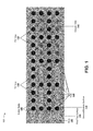
PCB 105 includes a substrate (e.g., a non-conductive substrate) that includes mechanical support for electronic components. Additionally, or alternatively, PCB 105 may include electrical connections for the electronic components using, for example, conductive tracks, pads, and/or other features etched from laminated sheets (e.g., copper sheets or sheets made from another conductive material). PCB 105 may include multiple layers, and conductors on different layers may be connected with vias 120. Additionally, or alternatively, PCB 105 may include a first surface 110 and a second surface 115 that is opposite the first surface 110 (e.g., located on an opposite or reverse side of PCB 105 as compared to first surface 110).
In some implementations, via 120 may not extend entirely through PCB 105 from the first surface 110 to the second surface 115. For example, via 120 may extend from the first surface 110 to an intermediate layer of PCB 105 (e.g., positioned between the first surface 110 and the second surface 115), may extend from the second surface 115 to an intermediate layer of PCB 105, or may extend from a first intermediate layer to a second intermediate layer. In some implementations, via 120 may extend from the second surface 115 to an intermediate layer of PCB 105, and via 120 may provide electrical connectivity for a component connected to the intermediate layer.
A set of solder balls 125 is an example of a mounting mechanism that may be used to mount an integrated circuit to the first surface 110 of PCB 105. In some implementations, other mounting mechanisms may be used, such as a surface-mount technology (SMT) mechanism (e.g., one or more pins, a pin grid array, one or more leads, one or more flat contacts, and/or the like), a through-hole technology (e.g., one or more leads on the integrated circuit may be inserted into vias 120), and/or the like.
TX via 130 serves as a via 120 used for transmission of a signal output by an integrated circuit mounted to the first surface 110 of PCB 105. In some implementations, PCB 105 may include a pair of TX vias 130 used to carry a differential pair of signals transmitted by the integrated circuit (e.g., for differential signaling). A differential pair of signals may refer to two signals that convey information based on a comparison of the two signals. For example, the pair of TX vias 130 may carry a differential pair of signals. A receiver may compare an electrical difference between the pair of signals, rather than the difference between a single signal and ground, thereby mitigating electromagnetic noise. As shown in FIG. 1 , PCB 105 may include multiple pairs of TX vias 130 (e.g., arranged according to a particular field pattern for high speed communication links). While TX via 130 is described herein as being a member (e.g., a part) of a TX differential pair, in some implementations, TX via 130 may include a TX via that is not a member of a TX differential pair.
RX via 135 serves as a via 120 used for reception of a signal to be received by an integrated circuit mounted to the first surface 110 of PCB 105. In some implementations, PCB 105 may include a pair of RX vias 135 used to carry a differential pair of signals to be received by the integrated circuit. As shown in FIG. 1 , PCB 105 may include multiple pairs of RX vias 135 (e.g., arranged according to a particular field pattern for high speed communication links). While RX via 135 is described herein as being a member (e.g., a part) of an RX differential pair, in some implementations, RX via 135 may include an RX via that is not a member of an RX differential pair.
Ground via 140 includes a via 120 used for electrical grounding of an integrated circuit mounted to the first surface 110 of PCB 105. In some implementations, ground via 140 may be used to carry a ground signal to the integrated circuit, may be used to provide a ground connection for power, and/or the like.
The number and arrangement of components shown in FIG. 1 are provided as an example. In practice, there may be additional components, fewer components, different components, or differently arranged components than those shown in FIG. 1 . Furthermore, two or more components shown in FIG. 1 may be implemented within a single components, or a single components shown in FIG. 1 may be implemented as multiple, distributed components. Additionally, or alternatively, a set of components (e.g., one or more components) shown in FIG. 1 may perform one or more functions described as being performed by another set of components shown in FIG. 1 .
In some implementations, a pair of wires 210 may carry a differential pair of signals. For example, a pair of wires 210 may be connected to a differential pair of TX vias 130 to carry a differential pair of signals transmitted by an integrated circuit mounted to the first surface 110 of PCB 105. Additionally, or alternatively, a pair of wires 210 may be connected to a differential pair of RX vias 135 to carry a differential pair of signals to be received by an integrated circuit mounted to the first surface 110 of PCB 105. In some implementations, a pair of wires 210 that carry a differential pair of signals may be bundled into a cable 215.
By mounting connector header 205 (e.g., a press-fit header) to the second surface 115 of PCB 105 to provide electrical connectivity for one or more components mounted to the first surface 110 of PCB 105, lower attenuation may be achieved using wires and/or cables connected to connectors supported by connector header 205 as compared to using PCB material to carry signals. Furthermore, one or more components used to mitigate attenuation of signals carried by the PCB material may be excluded from PCB 105, thereby increasing available space on PCB 105, reducing a size of PCB 105, reducing a power consumption of PCB 105, simplifying the design of PCB 105, and reducing the cost of PCB 105. Furthermore, mounting connector header 205 to the second surface 115 of PCB 105 allows for more physical space for one or more components and/or other cables connected to the first surface 110 of PCB 105, thereby further increasing available space on PCB 105, reducing a size of PCB 105, reducing a power consumption of PCB 105, simplifying the design of PCB 105, and reducing the cost of PCB 105.
The number and arrangement of components shown in FIG. 2 are provided as an example. In practice, there may be additional components, fewer components, different components, or differently arranged components than those shown in FIG. 2 . Furthermore, two or more components shown in FIG. 2 may be implemented within a single components, or a single components shown in FIG. 2 may be implemented as multiple, distributed components. Additionally, or alternatively, a set of components (e.g., one or more components) shown in FIG. 2 may perform one or more functions described as being performed by another set of components shown in FIG. 2 .
As shown in FIG. 3 , a first wire 210 of a cable 215 may be connected to a first via 120 using a first connector 310, and a second wire 210 of the cable 215 may be connected to a second via 120 using a second connector 310. For example, the first wire 210 may be connected to a first TX via 130 of a pair of TX vias 130 (e.g., using the first connector 310), and the second wire 210 may be connected to a second TX via 130 of the pair of TX vias 130 (e.g., using the second connector 310). As another example, the first wire 210 may be connected to a first RX via 135 of a pair of RX vias 135 (e.g., using the first connector 310), and the second wire 210 may be connected to a second RX via 135 of the pair of RX vias 135 (e.g., using the second connector 310). In either case, the first wire 210 may carry a first signal of a differential pair of signals, and the second wires 210 may carry a second signal of the differential pair of signals.
In some implementations, connector 310 may provide electrical connectivity for integrated circuit 305, such as when connector 310 is mated with a TX via 130 and/or an RX via 135, and when a wire 210 is connected to connector 310 and carries a signal to another device, such as transceiver 220. In some implementations, connector 310 may not provide electrical connectivity for integrated circuit 305, such as when no wire 210 is connected to connector 310. For example, connector 310 may be mated with a ground via 140, and may not be connected to a wire 210. In this case, connector 310 provides mechanical support for mounting connector header 205 to the second surface 115 of PCB 105, but does not provide electrical connectivity for integrated circuit 305.
By mounting connector header 205 (e.g., a press-fit header) to the second surface 115 of PCB 105 to provide electrical connectivity for one or more integrated circuits 305 mounted to the first surface 110 of PCB 105, lower attenuation may be achieved by carrying signals using wires 210 and/or cables 215 connected to connectors 310 as compared to using PCB material to carry the signals. Furthermore, as described elsewhere herein, this configuration may increase available space on PCB 105, may reduce a size of PCB 105, may reduce a power consumption of PCB 105, may simplify the design of PCB 105, and/or may reduce the cost of PCB 105.
Although described herein in relation to differential pairs of signals, connector header 205 may be used to connect to PCB 105 that supports components that transmit and/or receive other types of signals, in some implementations. In other words, connector header 205 is not specific to any type of signals, and may be used with a variety of PCBs 105.
The number and arrangement of components shown in FIG. 3 are provided as an example. In practice, there may be additional components, fewer components, different components, or differently arranged components than those shown in FIG. 3 . Furthermore, two or more components shown in FIG. 3 may be implemented within a single components, or a single components shown in FIG. 3 may be implemented as multiple, distributed components. Additionally, or alternatively, a set of components (e.g., one or more components) shown in FIG. 3 may perform one or more functions described as being performed by another set of components shown in FIG. 3 .
Implementations described herein include a connector header capable of being mounted to a bottom surface of a PCB to provide connectivity for components mounted to a top surface of the PCB. The connector header may include wires and/or cables that permit high speed communication of PCB components with lower attenuation than typical PCB materials. In this way, components used to mitigate attenuation of PCB materials may be excluded from the PCB, thereby increasing available space on the PCB, reducing PCB size, reducing PCB power consumption, simplifying PCB design, and reducing PCB cost. Furthermore, mounting the connector header to the bottom surface of the PCB reduces physical and/or electrical interference with components and/or other cables connected to the top surface of the PCB, thereby further increasing available space on the PCB, reducing PCB size, reducing PCB power consumption, simplifying PCB design, and reducing PCB cost.
The foregoing disclosure provides illustration and description, but is not intended to be exhaustive or to limit the implementations to the precise form disclosed. Modifications and variations are possible in light of the above disclosure or may be acquired from practice of the implementations.
Even though particular combinations of features are recited in the claims and/or disclosed in the specification, these combinations are not intended to limit the disclosure of possible implementations. In fact, many of these features may be combined in ways not specifically recited in the claims and/or disclosed in the specification. Although each dependent claim listed below may directly depend on only one claim, the disclosure of possible implementations includes each dependent claim in combination with every other claim in the claim set.
No element, act, or instruction used herein should be construed as critical or essential unless explicitly described as such. Also, as used herein, the articles “a” and “an” are intended to include one or more items, and may be used interchangeably with “one or more.” Furthermore, as used herein, the term “set” is intended to include one or more items (e.g., related items, unrelated items, a combination of related and unrelated items, etc.), and may be used interchangeably with “one or more.” Where only one item is intended, the term “one” or similar language is used. Also, as used herein, the terms “has,” “have,” “having,” or the like are intended to be open-ended terms. Further, the phrase “based on” is intended to mean “based, at least in part, on” unless explicitly stated otherwise.
Claims (20)
1. An apparatus, comprising:
a printed circuit board;
an integrated circuit mounted on a first surface of the printed circuit board;
one or more vias that extend through the printed circuit board from the first surface to a second surface of the printed circuit board to provide electrical connectivity for the integrated circuit,
the second surface of the printed circuit board being opposite the first surface of the printed circuit board; and
a pin header that mechanically supports one or more pins that provide electrical connectivity for the integrated circuit,
the pin header being mounted to the second surface of the printed circuit board to mate the one or more pins with the one or more vias to provide electrical connectivity for the integrated circuit, and
the one or more vias including a via that is mated with a pin, of the one or more pins, that does not provide electrical connectivity for the integrated circuit.
2. The apparatus of claim 1 , where the pin header is a press-fit header and the one or more pins are one or more press-fit pins.
3. The apparatus of claim 1 , further comprising:
one or more wires and/or cables attached to the one or more pins to provide a communication link for the integrated circuit.
4. The apparatus of claim 1 ,
where the via is a first via,
where the one or more vias further include a second via and a third via that carry a differential pair of signals used for differential signaling, and
where the first via is for electrical grounding.
5. The apparatus of claim 4 ,
where the pin is a first pin, and
where the apparatus further comprises:
a first wire connected to the second via using a second pin of the one or more pins,
the first wire being to carry a first signal of the differential pair of signals; and
a second wire connected to the third via using a third pin of the one or more pins,
the second wire being to carry a second signal of the differential pair of signals.
6. The apparatus of claim 4 ,
where the pin is a first pin, and
where the one or more pins further include:
a second pin, mated with the second via, that provides electrical connectivity for the integrated circuit; and
a third pin, mated with the third via, that provides electrical connectivity for the integrated circuit.
7. The apparatus of claim 1 , where the pin provides mechanical support for mounting the pin header to the second surface of the printed circuit board.
8. The apparatus of claim 1 , where the one or more vias include a plurality of vias arranged in an array according to a ball grid array pattern of solder balls positioned on the first surface of the printed circuit board.
9. An apparatus, comprising:
a printed circuit board having a first surface;
an array of vias that extend through the printed circuit board from the first surface to a second surface of the printed circuit board,
the array of vias to provide electrical connectivity for an integrated circuit to be mounted to the first surface of the printed circuit board; and
a connector header that mechanically supports a plurality of connectors,
the connector header being mounted to the second surface of the printed circuit board to mate the plurality of connectors with a corresponding plurality of vias, included in the array of vias, from the second surface of the printed circuit board,
at least one of the plurality of connectors to provide electrical connectivity for the integrated circuit.
10. The apparatus of claim 9 , where the connector header is a press-fit header and the plurality of connectors are a plurality of press-fit pins.
11. The apparatus of claim 9 , where the plurality of vias includes:
a first set of vias to carry a first differential pair of signals for transmission, and
a second set of vias to carry a second differential pair of signals for reception.
12. The apparatus of claim 11 , further comprising:
a first cable connected to the first set of vias using a first set of connectors of the plurality of connectors,
the first cable to carry the first differential pair of signals; and
a second cable connected to the second set of vias using a second set of connectors of the plurality of connectors,
the second cable to carry the second differential pair of signals.
13. The apparatus of claim 9 , where the plurality of vias includes:
a set of vias for electrical grounding.
14. The apparatus of claim 13 , where the set of vias are mated with a set of connectors, of the plurality of connectors, that provide mechanical support for mounting the connector header to the second surface of the printed circuit board and that do not provide electrical connectivity for the integrated circuit.
15. An apparatus, comprising:
a printed circuit board having a first surface for mounting an integrated circuit and a second surface opposite the first surface;
an array of vias to provide electrical connectivity for the integrated circuit,
the array of vias extending through the printed circuit board from the first surface to the second surface; and
a connector header that mechanically supports a plurality of connectors,
the connector header being mounted to the second surface of the printed circuit board,
the plurality of connectors being mated with the array of vias to provide electrical connectivity for the integrated circuit.
16. The apparatus of claim 15 , where the connector header is a press-fit header and the plurality of connectors are a plurality of press-fit pins.
17. The apparatus of claim 15 , where the connector header is a pogo pin header and the plurality of connectors are a plurality of pogo pins.
18. The apparatus of claim 15 , where the array of vias includes:
a first pair of vias to carry a first differential pair of signals for transmission, and
a second pair of vias to carry a second differential pair of signals for reception.
19. The apparatus of claim 18 , further comprising:
a first cable connected to the first pair of vias using a first pair of connectors of the plurality of connectors,
the first cable to carry the first differential pair of signals; and
a second cable connected to the second pair of vias using a second pair of connectors of the plurality of connectors,
the second cable to carry the second differential pair of signals.
20. The apparatus of claim 19 , where the first cable includes a first wire and a second wire to carry the first differential pair of signals, and
where the second cable includes a third wire and a fourth wire to carry the second differential pair of signals.
Priority Applications (1)
| Application Number | Priority Date | Filing Date | Title |
|---|---|---|---|
| US15/388,021 US10076033B1 (en) | 2016-12-22 | 2016-12-22 | Printed circuit board with connector header mounted to bottom surface |
Applications Claiming Priority (1)
| Application Number | Priority Date | Filing Date | Title |
|---|---|---|---|
| US15/388,021 US10076033B1 (en) | 2016-12-22 | 2016-12-22 | Printed circuit board with connector header mounted to bottom surface |
Publications (1)
| Publication Number | Publication Date |
|---|---|
| US10076033B1 true US10076033B1 (en) | 2018-09-11 |
Family
ID=63406555
Family Applications (1)
| Application Number | Title | Priority Date | Filing Date |
|---|---|---|---|
| US15/388,021 Active US10076033B1 (en) | 2016-12-22 | 2016-12-22 | Printed circuit board with connector header mounted to bottom surface |
Country Status (1)
| Country | Link |
|---|---|
| US (1) | US10076033B1 (en) |
Cited By (2)
| Publication number | Priority date | Publication date | Assignee | Title |
|---|---|---|---|---|
| US11482802B2 (en) | 2020-12-04 | 2022-10-25 | Cisco Technology, Inc. | High speed traceless interconnect |
| US20230050002A1 (en) * | 2021-08-13 | 2023-02-16 | Cisco Technology, Inc. | Integrated circuit interconnect techniques |
Citations (11)
| Publication number | Priority date | Publication date | Assignee | Title |
|---|---|---|---|---|
| US4315321A (en) * | 1978-06-16 | 1982-02-09 | The Kardios Systems Corporation | Method and apparatus for enhancing the capabilities of a computing system |
| US5767575A (en) | 1995-10-17 | 1998-06-16 | Prolinx Labs Corporation | Ball grid array structure and method for packaging an integrated circuit chip |
| US5859538A (en) | 1996-01-31 | 1999-01-12 | Hewlett-Packard Company | Method and apparatus for connecting a ball grid array device to a test instrument to facilitate the monitoring of individual signals or the interruption of individual signals or both |
| US5906042A (en) | 1995-10-04 | 1999-05-25 | Prolinx Labs Corporation | Method and structure to interconnect traces of two conductive layers in a printed circuit board |
| EP1085571A1 (en) | 1999-09-20 | 2001-03-21 | Texas Instruments Incorporated | Method for increasing device reliability of a BGA package |
| US6386429B1 (en) * | 1999-01-13 | 2002-05-14 | Calestica International Inc. | Printed circuit board header attachment station |
| US6399417B1 (en) | 2001-03-06 | 2002-06-04 | Siliconware Precision Industries Co., Ltd. | Method of fabricating plated circuit lines over ball grid array substrate |
| US6719573B2 (en) * | 2002-03-18 | 2004-04-13 | Molex Incorporated | Electrical connector assembly and method of assembling same |
| US20090034983A1 (en) * | 2007-07-31 | 2009-02-05 | Nec Corporation | Optical transmitter-receiver subassembly and optical transmitter-receiver module |
| US8845367B2 (en) * | 2006-04-05 | 2014-09-30 | Pulse Electronics, Inc. | Modular electronic header assembly and methods of manufacture |
| US20170079140A1 (en) * | 2015-09-11 | 2017-03-16 | Intel Corporation | System, apparatus and method for interconnecting circuit boards |
-
2016
- 2016-12-22 US US15/388,021 patent/US10076033B1/en active Active
Patent Citations (11)
| Publication number | Priority date | Publication date | Assignee | Title |
|---|---|---|---|---|
| US4315321A (en) * | 1978-06-16 | 1982-02-09 | The Kardios Systems Corporation | Method and apparatus for enhancing the capabilities of a computing system |
| US5906042A (en) | 1995-10-04 | 1999-05-25 | Prolinx Labs Corporation | Method and structure to interconnect traces of two conductive layers in a printed circuit board |
| US5767575A (en) | 1995-10-17 | 1998-06-16 | Prolinx Labs Corporation | Ball grid array structure and method for packaging an integrated circuit chip |
| US5859538A (en) | 1996-01-31 | 1999-01-12 | Hewlett-Packard Company | Method and apparatus for connecting a ball grid array device to a test instrument to facilitate the monitoring of individual signals or the interruption of individual signals or both |
| US6386429B1 (en) * | 1999-01-13 | 2002-05-14 | Calestica International Inc. | Printed circuit board header attachment station |
| EP1085571A1 (en) | 1999-09-20 | 2001-03-21 | Texas Instruments Incorporated | Method for increasing device reliability of a BGA package |
| US6399417B1 (en) | 2001-03-06 | 2002-06-04 | Siliconware Precision Industries Co., Ltd. | Method of fabricating plated circuit lines over ball grid array substrate |
| US6719573B2 (en) * | 2002-03-18 | 2004-04-13 | Molex Incorporated | Electrical connector assembly and method of assembling same |
| US8845367B2 (en) * | 2006-04-05 | 2014-09-30 | Pulse Electronics, Inc. | Modular electronic header assembly and methods of manufacture |
| US20090034983A1 (en) * | 2007-07-31 | 2009-02-05 | Nec Corporation | Optical transmitter-receiver subassembly and optical transmitter-receiver module |
| US20170079140A1 (en) * | 2015-09-11 | 2017-03-16 | Intel Corporation | System, apparatus and method for interconnecting circuit boards |
Cited By (2)
| Publication number | Priority date | Publication date | Assignee | Title |
|---|---|---|---|---|
| US11482802B2 (en) | 2020-12-04 | 2022-10-25 | Cisco Technology, Inc. | High speed traceless interconnect |
| US20230050002A1 (en) * | 2021-08-13 | 2023-02-16 | Cisco Technology, Inc. | Integrated circuit interconnect techniques |
Similar Documents
| Publication | Publication Date | Title |
|---|---|---|
| US9660369B2 (en) | Assembly of cable and connector | |
| US9437912B2 (en) | 3-D integrated package | |
| US10244629B1 (en) | Printed circuit board including multi-diameter vias | |
| US10062993B1 (en) | Flexible cable for pluggable modules | |
| US20190051587A1 (en) | Ic package | |
| CN108432355B (en) | Recess type circuit board | |
| US8410874B2 (en) | Vertical quasi-CPWG transmission lines | |
| US10455691B1 (en) | Grid array pattern for crosstalk reduction | |
| CN109587942B (en) | Clearance size reduction for backdrilled differential vias | |
| TW201112506A (en) | Lead arrangement, electric connector and electric assembly | |
| US20170018881A1 (en) | Pluggable connector and interconnection system configured for resonance control | |
| KR20170073323A (en) | Printed circuit board having high-speed signal connector | |
| US10470293B2 (en) | Printed circuit board and optical transceiver with the printed circuit board | |
| KR20210097837A (en) | Alternative circuit apparatus for long host routing | |
| US20240021970A1 (en) | Printed circuit boards and methods for manufacturing thereof for RF connectivity between electro-optic phase modulator and Digital Signal Processor | |
| US20190164891A1 (en) | Tunable differential via circuit | |
| US10076033B1 (en) | Printed circuit board with connector header mounted to bottom surface | |
| WO2023273757A1 (en) | Printed circuit board and electronic device | |
| CN114375614A (en) | Printed circuit board configuration for surface mount dual density QSFP connector footprint to facilitate belly-to-belly alignment | |
| JP2016506063A (en) | Electrical connection interface for connecting electrical leads for high-speed data transmission | |
| US8585432B2 (en) | Connector and optical transmission apparatus | |
| CN107026666B (en) | Wireless communication assembly | |
| US20150242356A1 (en) | PCI Express Expansion System | |
| US8465214B2 (en) | Arrangement comprising an electrical conductor track carrier and an optoelectronic component, and a method for producing such an arrangement | |
| US20210045244A1 (en) | Multiple circuit boards with high-density compression interconnect |
Legal Events
| Date | Code | Title | Description |
|---|---|---|---|
| STCF | Information on status: patent grant |
Free format text: PATENTED CASE |
|
| MAFP | Maintenance fee payment |
Free format text: PAYMENT OF MAINTENANCE FEE, 4TH YEAR, LARGE ENTITY (ORIGINAL EVENT CODE: M1551); ENTITY STATUS OF PATENT OWNER: LARGE ENTITY Year of fee payment: 4 |