US10074804B2 - Picene derivative, photoelectric material, and photoelectric device - Google Patents
Picene derivative, photoelectric material, and photoelectric device Download PDFInfo
- Publication number
- US10074804B2 US10074804B2 US15/504,425 US201515504425A US10074804B2 US 10074804 B2 US10074804 B2 US 10074804B2 US 201515504425 A US201515504425 A US 201515504425A US 10074804 B2 US10074804 B2 US 10074804B2
- Authority
- US
- United States
- Prior art keywords
- group
- optionally substituted
- photoelectric
- substituted hydrocarbon
- hydrocarbon group
- Prior art date
- Legal status (The legal status is an assumption and is not a legal conclusion. Google has not performed a legal analysis and makes no representation as to the accuracy of the status listed.)
- Expired - Fee Related
Links
- 0 *C.*C.C.C.[1*]C1=C([2*])C2=C(C=C1)C([3*])=C([4*])C1=C2C([5*])=C([6*])C=C1 Chemical compound *C.*C.C.C.[1*]C1=C([2*])C2=C(C=C1)C([3*])=C([4*])C1=C2C([5*])=C([6*])C=C1 0.000 description 25
- RUAKNOMQBFRAIV-UHFFFAOYSA-N C/C1=C/C2=C(S1)C1=C(C=CS1)C2.CC.CC.CC.CC.CC.CC1=C/C2=C(\C=C/1)C1=C(C=C3C(=C1)CC1=C3C=CC=C1)C2.CC1=C2N=CC=NC2=C(C)C2=C1N=CC=N2.CC1=C2N=CC=NC2=C(C)C2=NSN=C21.CC1=C2N=CC=NC2=C(C)S1.CC1=CC2=C(C=C3/C=C\CC3=C2)C1.CC1=CC2=C(S1)C1=C(C=C3C(=C1)CC1=C3SC=C1)C2.CC1=CC=CC2=NCN=C12 Chemical compound C/C1=C/C2=C(S1)C1=C(C=CS1)C2.CC.CC.CC.CC.CC.CC1=C/C2=C(\C=C/1)C1=C(C=C3C(=C1)CC1=C3C=CC=C1)C2.CC1=C2N=CC=NC2=C(C)C2=C1N=CC=N2.CC1=C2N=CC=NC2=C(C)C2=NSN=C21.CC1=C2N=CC=NC2=C(C)S1.CC1=CC2=C(C=C3/C=C\CC3=C2)C1.CC1=CC2=C(S1)C1=C(C=C3C(=C1)CC1=C3SC=C1)C2.CC1=CC=CC2=NCN=C12 RUAKNOMQBFRAIV-UHFFFAOYSA-N 0.000 description 3
- XOVQSUBEYPYGNM-UHFFFAOYSA-N BP(B)C.B[PH](C)=O.CCCCCCCCOC(=O)CCCC1(C2=CC=CC=C2)C23/C4=C5C6=C7\C8C9/C=C\C%10/C%11=C/C=C%12C%13=CC=C%14C%15=C%13/C%13=C(C\5=C\%15C5=C4C(=CCC%145)C2CCC9C713)\C6=C(\C%11=C\%12%13)C%108.CCCCOC(=O)CCCC1(C2=CC=CC=C2)C23/C4=C5C6=C7\C8C9/C=C\C%10/C%11=C/C=C%12C%13=CC=C%14C%15=C%13/C%13=C(C\5=C\%15C5=C4C(=CCC%145)C2CCC9C713)\C6=C(\C%11=C\%12%13)C%108.COC(=O)CCCC1(C2=CC=CC=C2)C23/C4=C5C6=C7\C8C9/C=C\C%10/C%11=C/C=C%12C%13=CC=C%14C%15=C%13/C%13=C(C\5=C\%15C5=C4C(=CCC%145)C2CCC9C713)\C6=C(\C%11=C\%12%13)C%108.COC(=O)CCCC1(C2=CC=CS2)C23/C4=C5C6=C7\C8C9/C=C\C%10/C%11=C/C=C%12C%13=CC=C%14C%15=C%13/C%13=C(C\5=C\%15C5=C4C(=CCC%145)C2CCC9C713)\C6=C(\C%11=C\%12%13)C%108 Chemical compound BP(B)C.B[PH](C)=O.CCCCCCCCOC(=O)CCCC1(C2=CC=CC=C2)C23/C4=C5C6=C7\C8C9/C=C\C%10/C%11=C/C=C%12C%13=CC=C%14C%15=C%13/C%13=C(C\5=C\%15C5=C4C(=CCC%145)C2CCC9C713)\C6=C(\C%11=C\%12%13)C%108.CCCCOC(=O)CCCC1(C2=CC=CC=C2)C23/C4=C5C6=C7\C8C9/C=C\C%10/C%11=C/C=C%12C%13=CC=C%14C%15=C%13/C%13=C(C\5=C\%15C5=C4C(=CCC%145)C2CCC9C713)\C6=C(\C%11=C\%12%13)C%108.COC(=O)CCCC1(C2=CC=CC=C2)C23/C4=C5C6=C7\C8C9/C=C\C%10/C%11=C/C=C%12C%13=CC=C%14C%15=C%13/C%13=C(C\5=C\%15C5=C4C(=CCC%145)C2CCC9C713)\C6=C(\C%11=C\%12%13)C%108.COC(=O)CCCC1(C2=CC=CS2)C23/C4=C5C6=C7\C8C9/C=C\C%10/C%11=C/C=C%12C%13=CC=C%14C%15=C%13/C%13=C(C\5=C\%15C5=C4C(=CCC%145)C2CCC9C713)\C6=C(\C%11=C\%12%13)C%108 XOVQSUBEYPYGNM-UHFFFAOYSA-N 0.000 description 1
- WPTLJWCMKNYZLG-UHFFFAOYSA-N C1=CC2=C(S1)C1=C(C=C2)C2=C(C=C1)C1=C(C=CS1)C=C2.CC(C)[Si](C1=CC2=C(S1)C1=C(C=C2)C2=C(C=C1)C1=C(C=C2)C=C([Si](C(C)C)(C(C)C)C(C)C)S1)(C(C)C)C(C)C Chemical compound C1=CC2=C(S1)C1=C(C=C2)C2=C(C=C1)C1=C(C=CS1)C=C2.CC(C)[Si](C1=CC2=C(S1)C1=C(C=C2)C2=C(C=C1)C1=C(C=C2)C=C([Si](C(C)C)(C(C)C)C(C)C)S1)(C(C)C)C(C)C WPTLJWCMKNYZLG-UHFFFAOYSA-N 0.000 description 1
- CBZREEXNXFSWTO-UHFFFAOYSA-N C=CCCCCCCCCCC.CCCCCCCC.CCCCCCCCCCCCC1=CC2=C(C=CC3=C2C=C(CCCCCCCCCCCC)C2=C3SC([Si](C(C)C)(C(C)C)C(C)C)=C2)C2=C1C=C([Si](C(C)C)(C(C)C)C(C)C)S2.CCCCN1/N=N\C2=CC=CC=C21.[H]B(F)(F)(F)F Chemical compound C=CCCCCCCCCCC.CCCCCCCC.CCCCCCCCCCCCC1=CC2=C(C=CC3=C2C=C(CCCCCCCCCCCC)C2=C3SC([Si](C(C)C)(C(C)C)C(C)C)=C2)C2=C1C=C([Si](C(C)C)(C(C)C)C(C)C)S2.CCCCN1/N=N\C2=CC=CC=C21.[H]B(F)(F)(F)F CBZREEXNXFSWTO-UHFFFAOYSA-N 0.000 description 1
- VMWIBARESAMRIZ-UHFFFAOYSA-N CC(C)[Si](C1=CC2=C(S1)C1=C(C=C2)C2=C(C=C1)C1=C(C=C2)C=C([Si](C(C)C)(C(C)C)C(C)C)S1)(C(C)C)C(C)C.CC1=CC2=C(C=CC3=C2C=C(C)C2=C3SC([Si](C(C)C)(C(C)C)C(C)C)=C2)C2=C1C=C([Si](C(C)C)(C(C)C)C(C)C)S2 Chemical compound CC(C)[Si](C1=CC2=C(S1)C1=C(C=C2)C2=C(C=C1)C1=C(C=C2)C=C([Si](C(C)C)(C(C)C)C(C)C)S1)(C(C)C)C(C)C.CC1=CC2=C(C=CC3=C2C=C(C)C2=C3SC([Si](C(C)C)(C(C)C)C(C)C)=C2)C2=C1C=C([Si](C(C)C)(C(C)C)C(C)C)S2 VMWIBARESAMRIZ-UHFFFAOYSA-N 0.000 description 1
- KWGXYZOQHREBAB-UHFFFAOYSA-N CC(C)[Si](C1=CC2=C(S1)C1=C(C=C2Br)C2=C(C=C1)C1=C(C=C([Si](C(C)C)(C(C)C)C(C)C)S1)C(Br)=C2)(C(C)C)C(C)C.CC1=CC2=C(C=CC3=C2C=C(C)C2=C3SC([Si](C(C)C)(C(C)C)C(C)C)=C2)C2=C1C=C([Si](C(C)C)(C(C)C)C(C)C)S2 Chemical compound CC(C)[Si](C1=CC2=C(S1)C1=C(C=C2Br)C2=C(C=C1)C1=C(C=C([Si](C(C)C)(C(C)C)C(C)C)S1)C(Br)=C2)(C(C)C)C(C)C.CC1=CC2=C(C=CC3=C2C=C(C)C2=C3SC([Si](C(C)C)(C(C)C)C(C)C)=C2)C2=C1C=C([Si](C(C)C)(C(C)C)C(C)C)S2 KWGXYZOQHREBAB-UHFFFAOYSA-N 0.000 description 1
- RUNFEBYUXTWAPR-UHFFFAOYSA-N CC1=C(Br)SC(C2=C(F)C(F)=C(C3=CC(C)=C(Br)S3)C3=NSN=C32)=C1.CCCCCCCCCCCCC1=CC2=C(C=CC3=C2C=C(CCCCCCCCCCCC)C2=C3SC(C3=C(C)C=C(C4=C(F)C(F)=C(C5=CC(C)=C(C)S5)C5=NSN=C54)S3)=C2)C2=C1C=C(C)S2.CCCCCCCCCCCCC1=CC2=C(C=CC3=C2C=C(CCCCCCCCCCCC)C2=C3SC([Sn](C)(C)C)=C2)C2=C1C=C(C)S2 Chemical compound CC1=C(Br)SC(C2=C(F)C(F)=C(C3=CC(C)=C(Br)S3)C3=NSN=C32)=C1.CCCCCCCCCCCCC1=CC2=C(C=CC3=C2C=C(CCCCCCCCCCCC)C2=C3SC(C3=C(C)C=C(C4=C(F)C(F)=C(C5=CC(C)=C(C)S5)C5=NSN=C54)S3)=C2)C2=C1C=C(C)S2.CCCCCCCCCCCCC1=CC2=C(C=CC3=C2C=C(CCCCCCCCCCCC)C2=C3SC([Sn](C)(C)C)=C2)C2=C1C=C(C)S2 RUNFEBYUXTWAPR-UHFFFAOYSA-N 0.000 description 1
- YLMWXMWLOSKLMG-UHFFFAOYSA-N CC1=CC2=C(S1)C1=C(C=C2)C2=C(C=C1)/C1=C(\C=C/2)/C=C(/C2=C(C)C=C(C3=C(F)C(F)=C(C4=CC(C)=C(C)S4)C4=NSN=C43)S2)S1 Chemical compound CC1=CC2=C(S1)C1=C(C=C2)C2=C(C=C1)/C1=C(\C=C/2)/C=C(/C2=C(C)C=C(C3=C(F)C(F)=C(C4=CC(C)=C(C)S4)C4=NSN=C43)S2)S1 YLMWXMWLOSKLMG-UHFFFAOYSA-N 0.000 description 1
- MFJTWCZYSUIEKD-DELWQQEKSA-N CC1C(=O)/C(=C2/C(=O)N(C)C3=C2C=CC(C2=CC=C(Br)S2)=C3)C2=C1C=C(C1=CC=C(Br)S1)C=C2.CCCCCCCCCCCCC1=CC2=C(C=CC3=C2C=C(CCCCCCCCCCCC)C2=C3SC(C3=CC=C(C4=C/C5=C(\C=C/4)/C(=C4\C(=O)N(C)C6=C4C=CC(C4=CC=C(C)S4)=C6)C(=O)N5C)S3)=C2)C2=C1C=C(C)S2.CCCCCCCCCCCCC1=CC2=C(C=CC3=C2C=C(CCCCCCCCCCCC)C2=C3SC([Sn](C)(C)C)=C2)C2=C1C=C(C)S2 Chemical compound CC1C(=O)/C(=C2/C(=O)N(C)C3=C2C=CC(C2=CC=C(Br)S2)=C3)C2=C1C=C(C1=CC=C(Br)S1)C=C2.CCCCCCCCCCCCC1=CC2=C(C=CC3=C2C=C(CCCCCCCCCCCC)C2=C3SC(C3=CC=C(C4=C/C5=C(\C=C/4)/C(=C4\C(=O)N(C)C6=C4C=CC(C4=CC=C(C)S4)=C6)C(=O)N5C)S3)=C2)C2=C1C=C(C)S2.CCCCCCCCCCCCC1=CC2=C(C=CC3=C2C=C(CCCCCCCCCCCC)C2=C3SC([Sn](C)(C)C)=C2)C2=C1C=C(C)S2 MFJTWCZYSUIEKD-DELWQQEKSA-N 0.000 description 1
- HLIKHVTVELECKN-UHFFFAOYSA-N CCCCCCCCC(CCCCCC)CC1=C(Br)SC(C2=CC=C(C3=CC(CC(CCCCCC)CCCCCCCC)=C(Br)S3)/C3=N/S/N=C\23)=C1.CCCCCCCCCCCCC1=CC2=C(C=CC3=C2C=C(CCCCCCCCCCCC)C2=C3SC(C3=C(CC(CCCCCC)CCCCCCCC)C=C(C4=CC=C(C5=CC(CC(CCCCCC)CCCCCCCC)=C(C)S5)C5=NSN=C45)S3)=C2)C2=C1C=C(C)S2.CCCCCCCCCCCCC1=CC2=C(C=CC3=C2C=C(CCCCCCCCCCCC)C2=C3SC([Sn](C)(C)C)=C2)C2=C1C=C(C)S2 Chemical compound CCCCCCCCC(CCCCCC)CC1=C(Br)SC(C2=CC=C(C3=CC(CC(CCCCCC)CCCCCCCC)=C(Br)S3)/C3=N/S/N=C\23)=C1.CCCCCCCCCCCCC1=CC2=C(C=CC3=C2C=C(CCCCCCCCCCCC)C2=C3SC(C3=C(CC(CCCCCC)CCCCCCCC)C=C(C4=CC=C(C5=CC(CC(CCCCCC)CCCCCCCC)=C(C)S5)C5=NSN=C45)S3)=C2)C2=C1C=C(C)S2.CCCCCCCCCCCCC1=CC2=C(C=CC3=C2C=C(CCCCCCCCCCCC)C2=C3SC([Sn](C)(C)C)=C2)C2=C1C=C(C)S2 HLIKHVTVELECKN-UHFFFAOYSA-N 0.000 description 1
- FGVGGRDPQVVZFC-UHFFFAOYSA-N CCCCCCCCCCCCC1=CC2=C(C=CC3=C2C=C(CCCCCCCCCCCC)C2=C3SC([Si](C(C)C)(C(C)C)C(C)C)=C2)C2=C1C=C([Si](C(C)C)(C(C)C)C(C)C)S2.CCCCCCCCCCCCC1=CC2=C(C=CC3=C2C=C(CCCCCCCCCCCC)C2=C3SC=C2)C2=C1C=CS2 Chemical compound CCCCCCCCCCCCC1=CC2=C(C=CC3=C2C=C(CCCCCCCCCCCC)C2=C3SC([Si](C(C)C)(C(C)C)C(C)C)=C2)C2=C1C=C([Si](C(C)C)(C(C)C)C(C)C)S2.CCCCCCCCCCCCC1=CC2=C(C=CC3=C2C=C(CCCCCCCCCCCC)C2=C3SC=C2)C2=C1C=CS2 FGVGGRDPQVVZFC-UHFFFAOYSA-N 0.000 description 1
- IEFWRUWPFYUUGJ-UHFFFAOYSA-N CCCCCCCCCCCCC1=CC2=C(C=CC3=C2C=C(CCCCCCCCCCCC)C2=C3SC([Sn](C)(C)C)=C2)C2=C1C=C(C)S2.CCCCCCCCCCCCC1=CC2=C(C=CC3=C2C=C(CCCCCCCCCCCC)C2=C3SC=C2)C2=C1C=CS2 Chemical compound CCCCCCCCCCCCC1=CC2=C(C=CC3=C2C=C(CCCCCCCCCCCC)C2=C3SC([Sn](C)(C)C)=C2)C2=C1C=C(C)S2.CCCCCCCCCCCCC1=CC2=C(C=CC3=C2C=C(CCCCCCCCCCCC)C2=C3SC=C2)C2=C1C=CS2 IEFWRUWPFYUUGJ-UHFFFAOYSA-N 0.000 description 1
- VBAAENWXPMREGV-UHFFFAOYSA-N CCCCCCCCCCCCC1=CC=C(C2N(C)CC34/C5=C6\C7=C8\C9C%10/C=C\C%11/C%12=C/C=C%13C%14=CC=C%15C%16=C%14/C%14=C(C\7=C(\C%12=C\%13%14)C%119)/C6=C\%16C6=C5C(=CCC%156)C3CCC%10C824)C=C1.COC(=O)CCCC1(C2=CC=CC=C2)C23C4=C5C6=C7/C8=C9\C=C6\C6C=CC%10C%11CCC%12C(=C\%11C12C%10C/56)/C1=C3\C2=C3C5=C(/C6=C\8C(C9)CC8=C6C5=C5C(C8)CC6CC%12\C1=C/3C56)/C7=C\42 Chemical compound CCCCCCCCCCCCC1=CC=C(C2N(C)CC34/C5=C6\C7=C8\C9C%10/C=C\C%11/C%12=C/C=C%13C%14=CC=C%15C%16=C%14/C%14=C(C\7=C(\C%12=C\%13%14)C%119)/C6=C\%16C6=C5C(=CCC%156)C3CCC%10C824)C=C1.COC(=O)CCCC1(C2=CC=CC=C2)C23C4=C5C6=C7/C8=C9\C=C6\C6C=CC%10C%11CCC%12C(=C\%11C12C%10C/56)/C1=C3\C2=C3C5=C(/C6=C\8C(C9)CC8=C6C5=C5C(C8)CC6CC%12\C1=C/3C56)/C7=C\42 VBAAENWXPMREGV-UHFFFAOYSA-N 0.000 description 1
Images


Classifications
-
- H01L51/0036—
-
- C—CHEMISTRY; METALLURGY
- C07—ORGANIC CHEMISTRY
- C07D—HETEROCYCLIC COMPOUNDS
- C07D495/00—Heterocyclic compounds containing in the condensed system at least one hetero ring having sulfur atoms as the only ring hetero atoms
- C07D495/02—Heterocyclic compounds containing in the condensed system at least one hetero ring having sulfur atoms as the only ring hetero atoms in which the condensed system contains two hetero rings
- C07D495/04—Ortho-condensed systems
-
- C—CHEMISTRY; METALLURGY
- C08—ORGANIC MACROMOLECULAR COMPOUNDS; THEIR PREPARATION OR CHEMICAL WORKING-UP; COMPOSITIONS BASED THEREON
- C08G—MACROMOLECULAR COMPOUNDS OBTAINED OTHERWISE THAN BY REACTIONS ONLY INVOLVING UNSATURATED CARBON-TO-CARBON BONDS
- C08G61/00—Macromolecular compounds obtained by reactions forming a carbon-to-carbon link in the main chain of the macromolecule
- C08G61/12—Macromolecular compounds containing atoms other than carbon in the main chain of the macromolecule
- C08G61/122—Macromolecular compounds containing atoms other than carbon in the main chain of the macromolecule derived from five- or six-membered heterocyclic compounds, other than imides
- C08G61/123—Macromolecular compounds containing atoms other than carbon in the main chain of the macromolecule derived from five- or six-membered heterocyclic compounds, other than imides derived from five-membered heterocyclic compounds
- C08G61/126—Macromolecular compounds containing atoms other than carbon in the main chain of the macromolecule derived from five- or six-membered heterocyclic compounds, other than imides derived from five-membered heterocyclic compounds with a five-membered ring containing one sulfur atom in the ring
-
- H01L51/0043—
-
- H01L51/0047—
-
- H—ELECTRICITY
- H10—SEMICONDUCTOR DEVICES; ELECTRIC SOLID-STATE DEVICES NOT OTHERWISE PROVIDED FOR
- H10K—ORGANIC ELECTRIC SOLID-STATE DEVICES
- H10K30/00—Organic devices sensitive to infrared radiation, light, electromagnetic radiation of shorter wavelength or corpuscular radiation
- H10K30/20—Organic devices sensitive to infrared radiation, light, electromagnetic radiation of shorter wavelength or corpuscular radiation comprising organic-organic junctions, e.g. donor-acceptor junctions
-
- H—ELECTRICITY
- H10—SEMICONDUCTOR DEVICES; ELECTRIC SOLID-STATE DEVICES NOT OTHERWISE PROVIDED FOR
- H10K—ORGANIC ELECTRIC SOLID-STATE DEVICES
- H10K85/00—Organic materials used in the body or electrodes of devices covered by this subclass
- H10K85/10—Organic polymers or oligomers
- H10K85/111—Organic polymers or oligomers comprising aromatic, heteroaromatic, or aryl chains, e.g. polyaniline, polyphenylene or polyphenylene vinylene
- H10K85/113—Heteroaromatic compounds comprising sulfur or selene, e.g. polythiophene
-
- H—ELECTRICITY
- H10—SEMICONDUCTOR DEVICES; ELECTRIC SOLID-STATE DEVICES NOT OTHERWISE PROVIDED FOR
- H10K—ORGANIC ELECTRIC SOLID-STATE DEVICES
- H10K85/00—Organic materials used in the body or electrodes of devices covered by this subclass
- H10K85/10—Organic polymers or oligomers
- H10K85/151—Copolymers
-
- H—ELECTRICITY
- H10—SEMICONDUCTOR DEVICES; ELECTRIC SOLID-STATE DEVICES NOT OTHERWISE PROVIDED FOR
- H10K—ORGANIC ELECTRIC SOLID-STATE DEVICES
- H10K85/00—Organic materials used in the body or electrodes of devices covered by this subclass
- H10K85/20—Carbon compounds, e.g. carbon nanotubes or fullerenes
- H10K85/211—Fullerenes, e.g. C60
- H10K85/215—Fullerenes, e.g. C60 comprising substituents, e.g. PCBM
-
- H—ELECTRICITY
- H10—SEMICONDUCTOR DEVICES; ELECTRIC SOLID-STATE DEVICES NOT OTHERWISE PROVIDED FOR
- H10K—ORGANIC ELECTRIC SOLID-STATE DEVICES
- H10K85/00—Organic materials used in the body or electrodes of devices covered by this subclass
- H10K85/60—Organic compounds having low molecular weight
- H10K85/649—Aromatic compounds comprising a hetero atom
- H10K85/655—Aromatic compounds comprising a hetero atom comprising only sulfur as heteroatom
-
- H—ELECTRICITY
- H10—SEMICONDUCTOR DEVICES; ELECTRIC SOLID-STATE DEVICES NOT OTHERWISE PROVIDED FOR
- H10K—ORGANIC ELECTRIC SOLID-STATE DEVICES
- H10K85/00—Organic materials used in the body or electrodes of devices covered by this subclass
- H10K85/60—Organic compounds having low molecular weight
- H10K85/649—Aromatic compounds comprising a hetero atom
- H10K85/657—Polycyclic condensed heteroaromatic hydrocarbons
- H10K85/6576—Polycyclic condensed heteroaromatic hydrocarbons comprising only sulfur in the heteroaromatic polycondensed ring system, e.g. benzothiophene
-
- C—CHEMISTRY; METALLURGY
- C08—ORGANIC MACROMOLECULAR COMPOUNDS; THEIR PREPARATION OR CHEMICAL WORKING-UP; COMPOSITIONS BASED THEREON
- C08G—MACROMOLECULAR COMPOUNDS OBTAINED OTHERWISE THAN BY REACTIONS ONLY INVOLVING UNSATURATED CARBON-TO-CARBON BONDS
- C08G2261/00—Macromolecular compounds obtained by reactions forming a carbon-to-carbon link in the main chain of the macromolecule
- C08G2261/10—Definition of the polymer structure
- C08G2261/12—Copolymers
- C08G2261/124—Copolymers alternating
-
- C—CHEMISTRY; METALLURGY
- C08—ORGANIC MACROMOLECULAR COMPOUNDS; THEIR PREPARATION OR CHEMICAL WORKING-UP; COMPOSITIONS BASED THEREON
- C08G—MACROMOLECULAR COMPOUNDS OBTAINED OTHERWISE THAN BY REACTIONS ONLY INVOLVING UNSATURATED CARBON-TO-CARBON BONDS
- C08G2261/00—Macromolecular compounds obtained by reactions forming a carbon-to-carbon link in the main chain of the macromolecule
- C08G2261/10—Definition of the polymer structure
- C08G2261/14—Side-groups
- C08G2261/141—Side-chains having aliphatic units
- C08G2261/1412—Saturated aliphatic units
-
- C—CHEMISTRY; METALLURGY
- C08—ORGANIC MACROMOLECULAR COMPOUNDS; THEIR PREPARATION OR CHEMICAL WORKING-UP; COMPOSITIONS BASED THEREON
- C08G—MACROMOLECULAR COMPOUNDS OBTAINED OTHERWISE THAN BY REACTIONS ONLY INVOLVING UNSATURATED CARBON-TO-CARBON BONDS
- C08G2261/00—Macromolecular compounds obtained by reactions forming a carbon-to-carbon link in the main chain of the macromolecule
- C08G2261/10—Definition of the polymer structure
- C08G2261/18—Definition of the polymer structure conjugated
-
- C—CHEMISTRY; METALLURGY
- C08—ORGANIC MACROMOLECULAR COMPOUNDS; THEIR PREPARATION OR CHEMICAL WORKING-UP; COMPOSITIONS BASED THEREON
- C08G—MACROMOLECULAR COMPOUNDS OBTAINED OTHERWISE THAN BY REACTIONS ONLY INVOLVING UNSATURATED CARBON-TO-CARBON BONDS
- C08G2261/00—Macromolecular compounds obtained by reactions forming a carbon-to-carbon link in the main chain of the macromolecule
- C08G2261/10—Definition of the polymer structure
- C08G2261/22—Molecular weight
- C08G2261/228—Polymers, i.e. more than 10 repeat units
-
- C—CHEMISTRY; METALLURGY
- C08—ORGANIC MACROMOLECULAR COMPOUNDS; THEIR PREPARATION OR CHEMICAL WORKING-UP; COMPOSITIONS BASED THEREON
- C08G—MACROMOLECULAR COMPOUNDS OBTAINED OTHERWISE THAN BY REACTIONS ONLY INVOLVING UNSATURATED CARBON-TO-CARBON BONDS
- C08G2261/00—Macromolecular compounds obtained by reactions forming a carbon-to-carbon link in the main chain of the macromolecule
- C08G2261/30—Monomer units or repeat units incorporating structural elements in the main chain
- C08G2261/32—Monomer units or repeat units incorporating structural elements in the main chain incorporating heteroaromatic structural elements in the main chain
- C08G2261/322—Monomer units or repeat units incorporating structural elements in the main chain incorporating heteroaromatic structural elements in the main chain non-condensed
- C08G2261/3223—Monomer units or repeat units incorporating structural elements in the main chain incorporating heteroaromatic structural elements in the main chain non-condensed containing one or more sulfur atoms as the only heteroatom, e.g. thiophene
-
- C—CHEMISTRY; METALLURGY
- C08—ORGANIC MACROMOLECULAR COMPOUNDS; THEIR PREPARATION OR CHEMICAL WORKING-UP; COMPOSITIONS BASED THEREON
- C08G—MACROMOLECULAR COMPOUNDS OBTAINED OTHERWISE THAN BY REACTIONS ONLY INVOLVING UNSATURATED CARBON-TO-CARBON BONDS
- C08G2261/00—Macromolecular compounds obtained by reactions forming a carbon-to-carbon link in the main chain of the macromolecule
- C08G2261/30—Monomer units or repeat units incorporating structural elements in the main chain
- C08G2261/32—Monomer units or repeat units incorporating structural elements in the main chain incorporating heteroaromatic structural elements in the main chain
- C08G2261/324—Monomer units or repeat units incorporating structural elements in the main chain incorporating heteroaromatic structural elements in the main chain condensed
- C08G2261/3241—Monomer units or repeat units incorporating structural elements in the main chain incorporating heteroaromatic structural elements in the main chain condensed containing one or more nitrogen atoms as the only heteroatom, e.g. carbazole
-
- C—CHEMISTRY; METALLURGY
- C08—ORGANIC MACROMOLECULAR COMPOUNDS; THEIR PREPARATION OR CHEMICAL WORKING-UP; COMPOSITIONS BASED THEREON
- C08G—MACROMOLECULAR COMPOUNDS OBTAINED OTHERWISE THAN BY REACTIONS ONLY INVOLVING UNSATURATED CARBON-TO-CARBON BONDS
- C08G2261/00—Macromolecular compounds obtained by reactions forming a carbon-to-carbon link in the main chain of the macromolecule
- C08G2261/30—Monomer units or repeat units incorporating structural elements in the main chain
- C08G2261/32—Monomer units or repeat units incorporating structural elements in the main chain incorporating heteroaromatic structural elements in the main chain
- C08G2261/324—Monomer units or repeat units incorporating structural elements in the main chain incorporating heteroaromatic structural elements in the main chain condensed
- C08G2261/3243—Monomer units or repeat units incorporating structural elements in the main chain incorporating heteroaromatic structural elements in the main chain condensed containing one or more sulfur atoms as the only heteroatom, e.g. benzothiophene
-
- C—CHEMISTRY; METALLURGY
- C08—ORGANIC MACROMOLECULAR COMPOUNDS; THEIR PREPARATION OR CHEMICAL WORKING-UP; COMPOSITIONS BASED THEREON
- C08G—MACROMOLECULAR COMPOUNDS OBTAINED OTHERWISE THAN BY REACTIONS ONLY INVOLVING UNSATURATED CARBON-TO-CARBON BONDS
- C08G2261/00—Macromolecular compounds obtained by reactions forming a carbon-to-carbon link in the main chain of the macromolecule
- C08G2261/30—Monomer units or repeat units incorporating structural elements in the main chain
- C08G2261/32—Monomer units or repeat units incorporating structural elements in the main chain incorporating heteroaromatic structural elements in the main chain
- C08G2261/324—Monomer units or repeat units incorporating structural elements in the main chain incorporating heteroaromatic structural elements in the main chain condensed
- C08G2261/3246—Monomer units or repeat units incorporating structural elements in the main chain incorporating heteroaromatic structural elements in the main chain condensed containing nitrogen and sulfur as heteroatoms
-
- C—CHEMISTRY; METALLURGY
- C08—ORGANIC MACROMOLECULAR COMPOUNDS; THEIR PREPARATION OR CHEMICAL WORKING-UP; COMPOSITIONS BASED THEREON
- C08G—MACROMOLECULAR COMPOUNDS OBTAINED OTHERWISE THAN BY REACTIONS ONLY INVOLVING UNSATURATED CARBON-TO-CARBON BONDS
- C08G2261/00—Macromolecular compounds obtained by reactions forming a carbon-to-carbon link in the main chain of the macromolecule
- C08G2261/40—Polymerisation processes
- C08G2261/41—Organometallic coupling reactions
-
- C—CHEMISTRY; METALLURGY
- C08—ORGANIC MACROMOLECULAR COMPOUNDS; THEIR PREPARATION OR CHEMICAL WORKING-UP; COMPOSITIONS BASED THEREON
- C08G—MACROMOLECULAR COMPOUNDS OBTAINED OTHERWISE THAN BY REACTIONS ONLY INVOLVING UNSATURATED CARBON-TO-CARBON BONDS
- C08G2261/00—Macromolecular compounds obtained by reactions forming a carbon-to-carbon link in the main chain of the macromolecule
- C08G2261/90—Applications
- C08G2261/91—Photovoltaic applications
-
- H01L51/4253—
-
- H—ELECTRICITY
- H10—SEMICONDUCTOR DEVICES; ELECTRIC SOLID-STATE DEVICES NOT OTHERWISE PROVIDED FOR
- H10K—ORGANIC ELECTRIC SOLID-STATE DEVICES
- H10K30/00—Organic devices sensitive to infrared radiation, light, electromagnetic radiation of shorter wavelength or corpuscular radiation
- H10K30/30—Organic devices sensitive to infrared radiation, light, electromagnetic radiation of shorter wavelength or corpuscular radiation comprising bulk heterojunctions, e.g. interpenetrating networks of donor and acceptor material domains
-
- H—ELECTRICITY
- H10—SEMICONDUCTOR DEVICES; ELECTRIC SOLID-STATE DEVICES NOT OTHERWISE PROVIDED FOR
- H10K—ORGANIC ELECTRIC SOLID-STATE DEVICES
- H10K30/00—Organic devices sensitive to infrared radiation, light, electromagnetic radiation of shorter wavelength or corpuscular radiation
- H10K30/50—Photovoltaic [PV] devices
-
- Y—GENERAL TAGGING OF NEW TECHNOLOGICAL DEVELOPMENTS; GENERAL TAGGING OF CROSS-SECTIONAL TECHNOLOGIES SPANNING OVER SEVERAL SECTIONS OF THE IPC; TECHNICAL SUBJECTS COVERED BY FORMER USPC CROSS-REFERENCE ART COLLECTIONS [XRACs] AND DIGESTS
- Y02—TECHNOLOGIES OR APPLICATIONS FOR MITIGATION OR ADAPTATION AGAINST CLIMATE CHANGE
- Y02E—REDUCTION OF GREENHOUSE GAS [GHG] EMISSIONS, RELATED TO ENERGY GENERATION, TRANSMISSION OR DISTRIBUTION
- Y02E10/00—Energy generation through renewable energy sources
- Y02E10/50—Photovoltaic [PV] energy
- Y02E10/549—Organic PV cells
-
- Y—GENERAL TAGGING OF NEW TECHNOLOGICAL DEVELOPMENTS; GENERAL TAGGING OF CROSS-SECTIONAL TECHNOLOGIES SPANNING OVER SEVERAL SECTIONS OF THE IPC; TECHNICAL SUBJECTS COVERED BY FORMER USPC CROSS-REFERENCE ART COLLECTIONS [XRACs] AND DIGESTS
- Y02—TECHNOLOGIES OR APPLICATIONS FOR MITIGATION OR ADAPTATION AGAINST CLIMATE CHANGE
- Y02P—CLIMATE CHANGE MITIGATION TECHNOLOGIES IN THE PRODUCTION OR PROCESSING OF GOODS
- Y02P70/00—Climate change mitigation technologies in the production process for final industrial or consumer products
- Y02P70/50—Manufacturing or production processes characterised by the final manufactured product
Definitions
- This invention relates to a noble p-type organic semiconductor material having a specific structure, a photoelectric material, and a photoelectric device using the same.
- inorganic solar cells including silicone-based and non-silicone-based solar cells and organic solar cells including dye-sensitized solar cells and organic thin film solar cells.
- organic solar cells are fabricated by film formation by a solution process, or printing, they can be produced at a lower cost and with a larger effective area.
- Another advantage of organic solar cells is that they can be made lighter than inorganic solar cells.
- an organic thin-film solar cell is suitably fabricated by a printing technique that is applicable to a plastic film substrate and is regarded as easily capable of taking on the form of a flexible device.
- organic solar cells often have low photoelectric efficiency, and the challenge is to increase the photoelectric efficiency.
- a bulk heterojunction formed of a blend of poly(3-hexylthiophene) (P3HT) as a p-type organic semiconductor material and [6,6]-phenyl-C61-butyric acid methyl ester (PCBM) as an n-type organic semiconductor material has been so far proposed as a material that can achieve high photoelectric efficiency in organic thin-film solar cells (see non-patent Literature 1, etc. listed below). While a low-molecular compound, such as pentacene, is used in some cases, a polymer material is generally considered as suited to fabricate a solution-processed device, and it is believed that using a polymer material as a p-type organic semiconductor material makes it easier to hold down the cost and increase the effective area.
- One of the characteristics demanded for a p-type organic semiconductor material is to contain a pi-conjugated system with high planarity.
- To have a highly planar pi-conjugated system in the material promises to benefit a strong pi-pi interaction and a high carrier transport efficiency and, as a result, provide high photovoltaic power.
- Patent Literatures 1 to 3 below disclose techniques relating to p-type organic polymer semiconductor materials.
- An object of the invention is to provide a p-type organic semiconductor material that is easy to prepare and has high planarity in its polymer structure.
- Another object of the invention is to provide a photoelectric layer, photoelectric device, and organic thin-film solar cell having high photoelectric efficiency by using the p-type organic semiconductor material.
- a picene derivative represented by general formula (1) is, when used as a p-type organic semiconductor material, capable of forming a photoelectric layer easily.
- the inventors' further study has led them to find that a photoelectric device having the photoelectric layer exhibits high carrier mobility and provides a solution to the above problem.
- the invention provides a new picene derivative comprising at least one constitutional unit represented by general formula (1) (hereinafter referred to as: a picene derivative)
- a 1 and A 2 each independently represent a monocyclic ring
- R 1 , R 2 , R 3 , R 4 , R 5 , and R 6 each independently represent a hydrogen atom, a halogen atom, a cyano group, a nitro group, a hydroxy group, a carboxyl group, a thiol group, —SiR 7 R 8 R 9 , —NR 10 R 11 , or an optionally substituted hydrocarbon group, provided that at least one of R 1 , R 2 , R 3 , R 4 , R 5 , and R 6 is not hydrogen; and R 7 , R 8 , R 9 , R 10 , and R 11 each independently represent a hydrogen atom or an optionally substituted hydrocarbon group.
- the invention provides a photoelectric material comprising (A) the picene derivative as a p-type organic semiconductor material and (B) an n-type organic semiconductor material.
- the invention provides a photoelectric material comprising (A) a p-type organic semiconductor material including at least one picene derivative and (B) an n-type organic semiconductor material.
- the invention provides a photoelectric layer obtained by film formation using the photoelectric material.
- the invention provides a photoelectric device comprising the photoelectric layer.
- the invention provides an organic thin film solar cell comprising the photoelectric device.
- the invention provides a novel picene derivative useful as an organic semiconductor material.
- the use of the photoelectric material of the invention, which contains the compound, provides high carrier mobility and accomplishes enhancement of device performance.
- FIG. 1( a ) is a cross-sectional view illustrating a structure of the photoelectric device of the invention.
- FIG. 1( b ) is a cross-sectional view illustrating another structure of the photoelectric device of the invention.
- FIG. 1( c ) is a cross-sectional view illustrating still another structure of the photoelectric device of the invention.
- the picene derivative of the invention is a compound having at least one constitutional unit represented by general formula (1) shown above.
- the asterisk * in formula (1) indicates the position at which the constitutional unit is linked to an adjacent group (hereinafter the same).
- the monocyclic ring represented by A 1 and A 2 in formula (1) is preferably, but not limited to, an aromatic monocyclic ring.
- the aromatic monocyclic ring include benzene, furan, thiophene, selenophene, tellurophene, thiazole, isothiazole, oxazole, isoxazole, pyridine, pyrazine, pyrimidine, pyridazine, pyrrole, imidazole, and pyrazole rings.
- a heterocyclic ring containing a sulfur, selenium, or tellurium atom is preferred for the improvement of device characteristics.
- R 1 , R 2 , R 3 , R 4 , R 5 , and R 6 each independently represent a hydrogen atom, a halogen atom, a cyano group, a nitro group, a hydroxy group, a carboxyl group, a thiol group, —SiR 7 R 8 R 9 , —NR 10 R 11 , or an optionally substituted hydrocarbon group, provided that at least one of them is not hydrogen, wherein R 7 , R 8 , R 9 , R 10 , and R 11 each independently represent a hydrogen atom or an optionally substituted hydrocarbon group.
- halogen atom in formula (1) examples include fluorine, chlorine, bromine, and iodine.
- hydrocarbon group in formula (1) examples include aromatic hydrocarbon groups, aromatic hydrocarbon groups substituted with an aliphatic hydrocarbon group, and aliphatic hydrocarbon groups.
- the hydrocarbon group preferably contains 1 to 40, more preferably 4 to 22, carbon atoms.
- aromatic hydrocarbon group examples include phenyl, naphthyl, cyclohexylphenyl, biphenyl, terphenyl, fluorenyl, thiophenylphenyl, furanylphenyl, 2′-phenyl-propylphenyl, benzyl, and naphthylmethyl.
- Examples of the aliphatic hydrocarbon group include straight-chain, branched, or cyclic alkyl groups, such as methyl, ethyl, propyl, isopropyl, butyl, s-butyl, t-butyl, isobutyl, amyl, isoamyl, t-amyl, hexyl, heptyl, isoheptyl, t-heptyl, n-octyl, isooctyl, t-octyl, nonyl, cyclopropyl, cyclobutyl, cyclopentyl, cyclohexyl, cycloheptyl, cyclooctyl, cyclononyl, and cyclodecyl.
- straight-chain, branched, or cyclic alkyl groups such as methyl, ethyl, propyl, isopropyl, butyl, s
- the aliphatic hydrocarbon group may be interrupted by —O—, —COO—, —OCO—, —CO—, —S—, —SO—, —SO 2 —, —NR 15 , —HC ⁇ CH—, or —C ⁇ C—.
- the interrupting group may interrupt the bond at which the aliphatic hydrocarbon group is bonded.
- R 15 represents an optionally substituted hydrocarbon group, examples of which include those recited above.
- R 15 is preferably perfluoroalkyl.
- aromatic hydrocarbon group substituted with an aliphatic hydrocarbon group examples include phenyl, naphthyl, and benzyl each substituted with any of the above described aliphatic hydrocarbon groups.
- substituents that may be bonded to the hydrocarbon groups include a halogen atom, a cyano group, a nitro group, a hydroxy group, a carboxyl group, a thiol group, and —NR′R′′ wherein R′ and R′′ each represent an optionally substituted hydrocarbon group, the examples of which include those recited above.
- the picene derivatives preferred are those having 2 to 100 constitutional units represented by general formula (1) for their excellent film-forming properties.
- the picene derivative may have a constitutional unit other than the one represented by formula (1) (hereinafter referred to as other constitutional unit).
- the ratio of the constitutional unit of the formula (1) is preferably 5 to 100 mol %, more preferably 10 to 90 mol %, even more preferably 20 to 80 mol %.
- picene derivatives of formula (1) preferred are those represented by general formula (1-1) or (1-2) shown below for ease of preparation.
- a 3 and A 4 each represent a 6-membered ring selected from the examples of the monocyclic ring represented by A 1 and A 2 ;
- a 5 and A 6 each represent a 5-membered ring selected from the examples of the monocyclic ring represented by A 1 and A 2 ;
- R 1 , R 2 , R 3 , R 4 , R 5 , and R 6 are as defined with respect to formula (1), provided that at least one of R 1 , R 2 , R 3 , R 4 , R 5 , and R 6 is not hydrogen.
- picene derivatives of formulae (1-1) and (1-2) preferred in terms of ease of preparation are those of formula (1-1) in which A 3 and A 4 are the same 6-membered ring and those of formula (1-2) in which A 5 and A 6 are the same 5-membered ring.
- the other constitutional unit is not particularly limited as long as it is a pi-conjugated group.
- Examples of the other constitutional unit include those of group Y and group Z shown below.
- the constitutional units (Y-2), (Y-3), and (Y-4) and constitutional units selected from group Z are preferred in the interests of material durability and light resistance.
- X 1 and X 4 each represent S, O, or NR 12 ; k represents an integer of 1 to 4; R 12 represents an optionally substituted hydrocarbon group; the hydrogen atom of the constitutional units of group Y is optionally replaced with a halogen atom, a cyano group, a nitro group, a hydroxy group, a carboxyl group, a thiol group, —NR 13 R 14 , an optionally substituted hydrocarbon group, or an optionally substituted heterocyclic group; and R 13 and R 14 each represent an optionally substituted hydrocarbon group.
- X 2 represents S or NR 15 ;
- X 3 represents S, NR 15 , CR 16 R 17 , or SiR 16 R 17 ;
- X 5 represents S, O, or NR 15 ;
- R 15 , R 16 , and R 17 each represent an optionally substituted hydrocarbon group;
- the hydrogen atom of the constitutional units of group Z is optionally replaced with a halogen atom, a cyano group, a nitro group, a hydroxy group, a carboxyl group, a thiol group, —NR 18 R 19 , an optionally substituted hydrocarbon group, or an optionally substituted heterocyclic group;
- R 18 and R 19 each represent an optionally substituted hydrocarbon group.
- Examples of the hydrocarbon group that may replace the hydrogen atom of the constitutional units included in groups Y and Z and the optionally substituted hydrocarbon group as represented by R 12 (of NR 12 represented by X 1 and X 4 in group Y), R 15 (in group Z and of NR 15 as represented by X 2 and X 5 and of NR 15 as represented by X 3 in group Z), and R 16 and R 17 (of CR 16 R 17 and SiR 16 R 17 as represented by X 3 in group Z) are the same as those of the optionally substituted hydrocarbon group in formula (1).
- the picene derivative contains the constitutional unit selected from groups Y and Z
- the picene derivative is represented by general formula (1′) shown below.
- the sequence of the o, p, and q constitutional units is not particularly restricted, and the effects of the invention are produced irrespective of the sequence.
- the ratios of the constitutional units when the number o of the constitutional unit of formula (1) is taken as 1, the number p of the constitutional units of group Y and the number q of the constitutional units of group Z are each preferably 1 to 10.
- the number p is more preferably 0 to 8, even more preferably 1 to 5, in the interests of light absorption efficiency in a long wavelength region.
- the number q is more preferably 0 to 2, even more preferably 1 to 2, most preferably 1, in view of light absorption efficiency in a long wavelength region.
- Y represents a group selected from group Y
- Z represents a group selected from group Z: o is a number of 1 to 1000; and p and q are each a number of 0 to 1000.
- Preferred examples of the picene derivative are compounds represented by general formula (2) below, particularly compounds represented by general formula (2-1) or (2-2):
- a 1 , A 2 , R 1 , R 2 , R 3 , R 4 , R 5 , and R 6 are as defined above with respect to formula (1); at least one R 1 , R 2 , R 3 , R 4 , R 5 , and R 6 is not hydrogen; Y 1 and Y 2 each represent a single bond or a combination of 1 to 5 groups selected from (Y-1) to (Y-8) below linked to each other; Z 1 represents a single bond or a group selected form (Z-1) to (Z-21) below; and n represents an integer of 1 to 1000.
- X 1 and X 4 each represent S, O, or NR 12 ; k represents an integer 1 to 4; R 12 represents an optionally substituted hydrocarbon group; the hydrogen atom of the groups (Y-1) to (Y-4) and (Y-6) to (Y-8) is optionally replaced with a halogen atom, a cyano group, a nitro group, a hydroxy group, a carboxyl group, a thiol group, —NR 13 R 14 , an optionally substituted hydrocarbon group, or an optionally substituted heterocyclic group; and R 13 and R 14 each represent an optionally substituted hydrocarbon group.
- X 2 represents S or NR 15
- X 3 represents S, NR 15 , CR 16 R 17 , or SiR 16 R 17
- X 5 represents S, O, or NR 15
- R 15 , R 16 , and R 17 each represent an optionally substituted hydrocarbon group
- the hydrogen atom of the groups (Z-1) to (Z-21) is optionally replaced with a halogen atom, a cyano group, a nitro group, a hydroxy group, a carboxyl group, a thiol group, —NR 18 R 19 , an optionally substituted hydrocarbon group, or an optionally substituted heterocyclic group
- R 18 and R 19 each represent an optionally substituted hydrocarbon group.
- a 1 , A 2 , R 1 , R 2 , R 3 , R 4 , R 5 , and R 6 are as defined above with respect to formula (1); A 3 and A 4 are as defined with respect to formula (1-1); A 5 and A 6 are as defined with respect to formula (1-2); Y 1 , Y 2 , Z 1 , and n are as defined with respect to formula (2); and at least one of R 1 , R 2 , R 3 , R 4 , R 5 , and R 6 is not hydrogen.
- R 1 , R 2 , R 3 , R 4 , R 5 , and R 6 is a substituent ( ⁇ H). While the effects of the invention are produced irrespective of the selection of the substituent R 1 , R 2 , R 3 , R 4 , R 5 , or R 6 , it is preferred that at least one of R 1 , R 2 , R 3 , R 4 , R 5 , and R 6 be C1-C30 unsubstituted alkyl or C1-C30 substituted alkyl, the methylene moiety of the substituted or unsubstituted alkyl may be —CH ⁇ CH— or the substituent on the alkyl group being selected from alkoxy, alkylthio, aryl, aryloxy, arylthio, heterocyclic group, acyl, acyloxy, amino, sulfonyl, carboxyl, cyano, sulfo,
- R 1 , R 2 , R 3 , R 4 , R 5 , and R 6 be C1-C30 unsubstituted alkyl or C1-C30 substituted alkyl, particularly C10-C20 substituted or unsubstituted alkyl.
- R 1 , R 2 , R 3 , R 4 , R 5 , and R 6 is a substituent H
- R 1 , R 3 , R 4 , and R 6 be a substituent, more preferably R 1 and R 6 be a substituent.
- the picene derivative include, but are not limited to, compound Nos. 1 through 17 shown below.
- R 1 , R 2 , R 3 , R 4 , R 5 , and R 6 are as defined with respect to formula (1);
- n is as defined with respect to formula (2);
- Hex represents hexyl;
- 2-EH represents 2-ethylhexyl;
- 2-HD represents 2-hexyldecyl;
- 2-OD represents 2-octyldodecyl.
- the picene derivative of the invention may be prepared by any method making use of commonly known reactions.
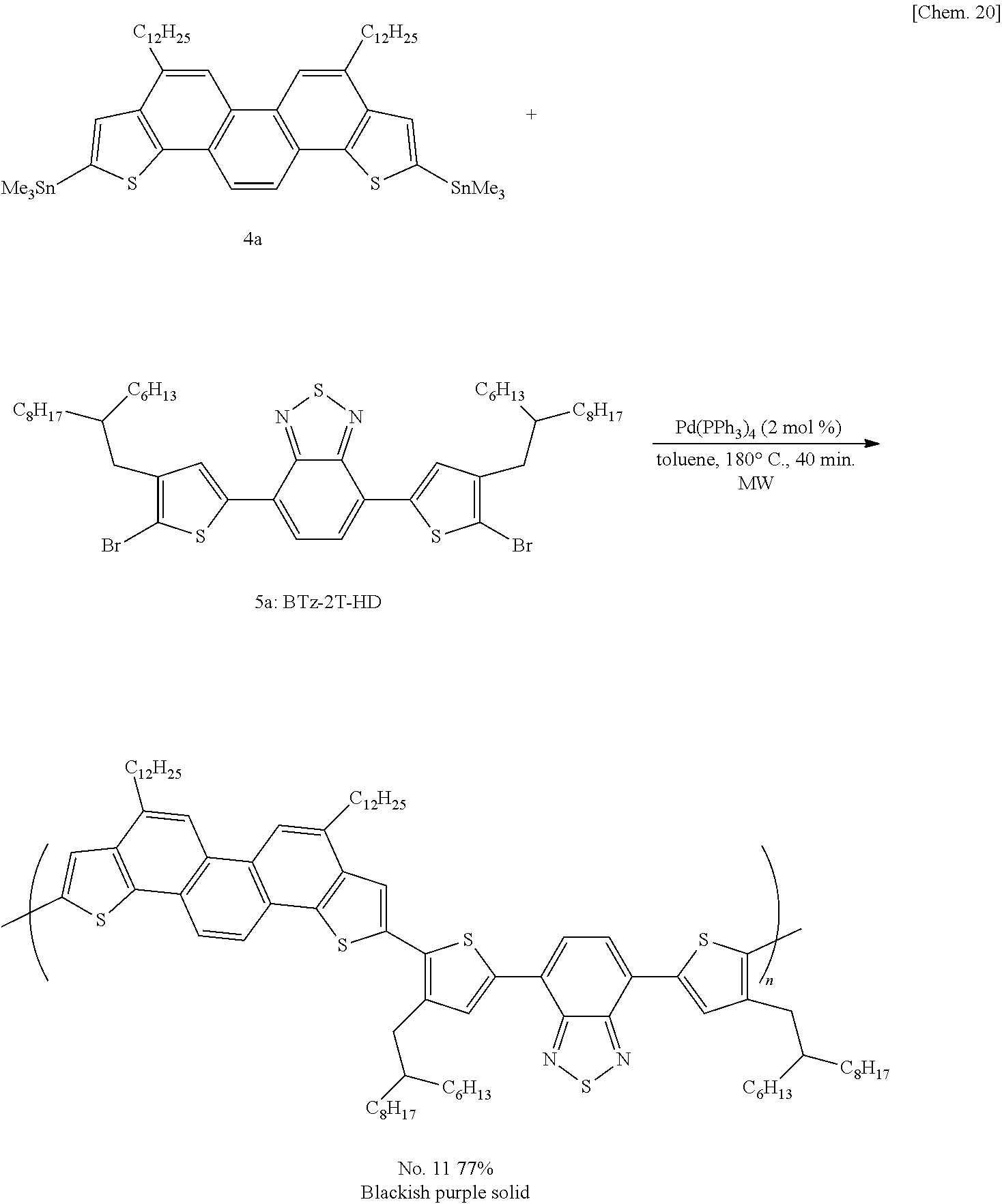
- the picene derivative of formula (2) can be prepared by polycondensation reaction between a bistrimethyltin compound (4) derived from a starting picene derivative (3) and a halogenated pi-conjugated compound (5) obtained by a known synthesis method in accordance with the following reaction scheme:
- a 1 , A 2 , R 1 , R 2 , R 3 , R 4 , R 5 , R 6 , Y 1 , Y 2 , Z 1 , and n are as defined with respect to formula (2).
- the picene derivative of the invention is suited not only as an organic semiconductor material but also for other uses, such as an antioxidant.
- the photoelectric material of the invention contains (A) a p-type organic semiconductor material containing at least one picene derivative of the invention and (B) an n-type organic semiconductor material.
- the p-type organic semiconductor material (A), which should contain at least one picene derivative of the invention, may further contain other known materials.
- the above description of the picene derivative applies appropriately to the picene derivative to be used in the photoelectric material.
- the known materials include phthalocyanine pigments, indigo or thioindigo pigments, quinacridone pigments, triarylmethane derivatives, triarylamines derivatives, oxazole derivatives, hydrazine derivatives, stilbene derivatives, pyrazoline derivatives, polysilane derivatives, polyphenylenevinylene and its derivatives (e.g., poly[2-methoxy-5-(2-ethylhexyloxy)-1,4-phenylenevinylene] (MEH-PPV) and poly[2-methoxy-5-(3′,7′-dimethyloctyloxy)-1,4-phenyelnevinylene]), polythiophene and its derivatives (e.g.
- the picene derivative content in the p-type organic semiconductor material (A) is preferably 1 to 99 mass %, more preferably 1 to 80 mass %.
- n-type organic semiconductor materials examples include perylene pigments, perinone pigments, polycyclic quinone pigments, azo pigments, and fullerene C60 or C70 and their derivatives. Additionally included are organic metal complexes (e.g., tris(8-quinolinolato)aluminum, bis(10-benzo[h]quinolinolato)beryllium, 5-hydroxyflavone beryllium salt, and 5-hydroxyflavone aluminum salt), oxadiazole derivatives (e.g., 1,3-bis[5′-(p-t-butylphenyl)-1,3,4-oxadiazol-2′-yl]benzene), triazole derivatives (e.g., 3-(4′-t-butylphenyl)-4-phenyl-5-(4′′-biphenyl)-1,2,4-triazole), phenanthroline derivatives (e.g., 2,9-dimethyl-4,7
- n-type organic semiconductor materials (B) described above preferred are fullerene C60, fullerene C70, and their derivatives for their high carrier mobility and/or high charge separation efficiency as an n-type material.
- the compounds listed above as an n-type organic semiconductor material may be used either individually or in combination of two or more thereof.
- fullerene C60, fullerene C70 or their derivatives include compounds C1 to C6 shown below. Preferred of them is compound C1, i.e., phenyl-C61-butyric acid methyl ester (PCBM).
- PCBM phenyl-C61-butyric acid methyl ester
- the weight ratio of component (A) to component (B) in the photoelectric material of the invention is 10:90 to 90:10, preferably 10:90 to 70:30, more preferably 20:80 to 50:50.
- the photoelectric material of the invention may contain one or more solvents.
- Any solvent capable of dissolving or dispersing components (A) and (B) may be used.
- useful solvents include water, alcohols, diols, ketones, esters, ethers, aliphatic or alicyclic hydrocarbons, aromatic hydrocarbons, cyano-containing hydrocarbons, halogenated hydrocarbons, and others.
- a photoelectric material containing a solvent is useful as a coating solution.
- Examples of the alcohols include methanol, ethanol, propanol, isopropyl alcohol, 1-butanol, isobutanol, 2-butanol, t-butanol, pentanol, isopentanol, 2-pentanol, neopentanol, t-pentanol, hexanol, 2-hexanol, heptanol, 2-heptanol, octanol, 2-ethylhexanol, 2-octanol, cyclopentanol, cyclohexanol, cycloheptanol, methylcyclopentanol, methylcyclohexanol, methylcycloheptanol, benzyl alcohol, ethylene glycol monomethyl ether, ethylene glycol monoethyl ether, propylene glycol monomethyl ether, propylene glycol monoethyl ether, diethylene glycol
- diols examples include ethylene glycol, propylene glycol, 1,2-butanediol, 1,3-butanediol, 1,4-butanediol, 1,5-pentanediol, neopentyl glycol, isoprene glycol (3-methyl-1,3-buanediol), 1,2-hexanediol, 1,6-hexanediol, 3-methyl-1,5-pentanediol, 1,2-octanediol, octanediol (2-ethyl-1,3-hexanediol), 2-butyl-2-ethyl-1,3-propanediol, 2,5-dimethyl-2,5-hexanediol, 1,2-cyclohexanediol, 1,4-cyclohexanediol, and 1,4-cyclohexanedimethanol.
- ketones examples include acetone, ethyl methyl ketone, methyl isopropyl ketone, methyl butyl ketone, methyl isobutyl ketone, methyl amyl ketone, methyl hexyl ketone, ethyl butyl ketone, diethyl ketone, dipropyl ketone, diisobutyl ketone, methyl amyl ketone, cyclohexanone, and methylcyclohexanone.
- esters examples include methyl formate, ethyl formate, methyl acetate, ethyl acetate, isopropyl acetate, butyl acetate, isobutyl acetate, s-butyl acetate, t-butyl acetate, amyl acetate, isoamyl acetate, t-amyl acetate, phenyl acetate, methyl propionate, ethyl propionate, isopropyl propionate, butyl propionate, isobutyl propionate, s-butyl propionate, t-butyl propionate, amyl propionate, isoamyl propionate, t-amyl propionate, phenyl propionate, methyl 2-ethylhexanoate, ethyl 2-ethylhexanolate, propyl 2-ethylhexanoate, isopropyl
- ethers examples include tetrahydrofuran, tetrahydropyran, morpholine, ethylene glycol dimethyl ether, diethylene glycol dimethyl ether, dipropylene glycol dimethyl ether, triethylene glycol dimethyl ether, dibutyl ether, diethyl ether, and dioxane.
- aliphatic or alicyclic hydrocarbons examples include pentane, hexane, cyclohexane, methylcyclohexane, dimethylcyclohexane, ethylcyclohexane, heptane, octane, decaline, solvent naphtha, terpene oil, D-limonene, pinene, mineral spirit, Swasol 310 (from Cosmo Oil), and Solvesso 100 (from Exxon Chemical).
- aromatic hydrocarbons examples include benzene, toluene, ethylbenzene, xylene, mesitylene, diethylbenzene, cumene, isobutylbenzene, cymene, and tetralin.
- cyano-containing hydrocarbons examples include acetonitrile, 1-cyanopropane, 1-cyanobutane, 1-cyanohexane, cyanocyclohexane, cyanobenzene, 1,3-dicyanopropane, 1,4-dicyanobutane, 1,6-dicyanohexane, 1,4-dicyanocyclohexane, and 1,4-dicyanobenzene.
- halogenated hydrocarbons examples include carbon tetrachloride, chloroform, trichloroethylene, chlorobenzene, dichlorobenzene, and trichlorobenzene.
- the other organic solvents include N-methyl-2-pyrrolidone, dimethyl sulfoxide, dimethylformamide, aniline, triethylamine, pyridine, and carbon disulfide.
- chloroform a compound selected from the group consisting of benzene, benzylene, chlorobenzene, dichlorobenzene, and trichlorobenzene.
- the content of the organic solvent in the photoelectric material of the invention is not particularly limited as long as the photoelectric material is capable of forming a photoelectric layer.
- a preferred solvent content is such that the total amount of components (A) and (B) in the photoelectric material may range from 0.1 to 20 parts by weight, more preferably 1 to 10 parts by weight, even more preferably 3 to 7 parts by weight, per 100 parts by weight of the solvent.
- the photoelectric layer of the invention is obtained by film formation techniques using the photoelectric material of the invention.
- Film formation techniques for forming a coating film on a substrate include, but are not limited to, dry processes, such as vapor deposition, physical vapor growth (PVD), chemical vapor growth (CVD), atomic layer deposition (ALD), atomic layer epitaxy (ALE), molecular beam epitaxy (MBE), vapor phase epitaxy (VPE), sputtering, and plasma polymerization; and wet processes, such as dip coating, casting, air knife coating, curtain coating, roller coating, wire bar coating, gravure coating, spin coating, LB process, offset printing, screen printing, flexography, dispenser printing, ink jet printing, and extrusion coating.
- dry processes such as vapor deposition, physical vapor growth (PVD), chemical vapor growth (CVD), atomic layer deposition (ALD), atomic layer epitaxy (ALE), molecular beam epitaxy (MBE), vapor phase epitaxy (VPE), s
- the thickness of the photoelectric layer is usually preferably, but not limited to, about 5 nm to 5 ⁇ m.
- the layer may be subjected to a heat treatment, such as annealing.
- the photoelectric layer is used in devices in which a blend of a p-type and an n-type organic semiconductor material is used, including not only organic bulk heterojunction devices, which are preferred embodiments, but super-hierarchical nanostructure junction devices, hybrid heterojunction devices, and the i-type layer of p-i-n junction devices.
- the photoelectric device of the invention is structurally equal to conventionally known photoelectric devices, except for containing at least one photoelectric layer of the invention. Taking, for instance, the structure shown in FIG. 1( a ) , it has a support 1 , an electrode 2 , a charge transfer layer 3 , a photoelectric layer 4 , and an electrode 5 stacked in the order described.
- the photoelectric device may have a structure having no charge transfer layer 3 as illustrated in FIG. 1( b ) or a structure having an additional charge transfer layer 6 as illustrated in FIG. 1( c ) .
- the photoelectric device of the invention should transmit light from the side of the support 1 to the photoelectric layer 4 .
- the support 1 , the electrode 2 , and the charge transfer layer 3 be made of a light transmissive material and have a transmittance of at least 70%.
- the support 1 is not limited by material and thickness as long as it is capable of stably supporting the electrode 2 on its surface but should be transparent.
- the support may be a plate or a film.
- transparent means capable of transmitting light of a predetermined wavelength region used for photoelectric devices, for example, visible light at high transmittances.
- the support 1 include glass and transparent film of polymers, such as polyethylene terephthalate (PET), tetraacetyl cellulose (TAC), polycarbonate, polyethylene naphthalate, polyphenylene sulfide, polyester sulfone, and syndiotactic polystyrene.
- the electrode 2 may be configured to double as the support 1 when the electrode 2 itself is a self-supporting layer with certain hardness. In such a case, the support 1 may be omitted.
- the mutually facing electrodes are related to each other such that the work function of one of them is greater than that of the other, namely these electrodes have different work functions. Accordingly, the work function of the electrode 2 may be relatively greater than that of the electrode 5 . In this case, the difference in work function between the two electrodes is preferably 0.5 V or greater. In the case where a buffer layer is provided between each electrode and the adjacent semiconductor layer, and a compound of the buffer layer and the electrode are chemically bonded to each other, the above described restriction may sometimes be alleviated.
- the electrodes 2 and 5 may be made of appropriately selected materials, including noble metals, e.g., gold, platinum, and silver; metal oxides, e.g., zinc oxide, indium oxide, tin oxide (NESA®), tin-doped indium oxide (ITO), and fluorine-doped tin oxide (FTO); lithium, lithium-indium alloys, sodium, sodium-potassium alloys, calcium, magnesium, magnesium-silver alloys, magnesium-indium alloys, indium, ruthenium, titanium, manganese, yttrium, aluminum, aluminum-lithium alloys, aluminum-calcium alloys, aluminum-magnesium alloys, chromium, graphite; and organic conductive compounds, such as poly(3,4-ethylenedioxythiophene)-poly(styrene sulfonate) (PEDOT:PSS).
- PEDOT:PSS poly(3,4-ethylenedioxythiophene)-poly(styrene
- Electrode materials may be used either individually or as a mixture of two or more thereof. Since the electrode 2 must be transparent, transparent materials, such as zinc oxide, NESA, ITO, FTO, and PEDOT:PSS, are used.
- the electrodes 2 and 5 can be formed using these electrode materials by a dry or wet process similarly to the photoelectric layer 4 .
- the electrodes 2 and 5 may also be formed through firing, for example, by the sol-gel process.
- the thickness of the electrodes 2 and 5 while varying depending on the material, usually ranges from about 5 to 1000 nm, preferably from about 10 to 500 nm.
- the charge transfer layers 3 and 6 each serves to prevent the electrode material from entering and reacting with the photoelectric layer and to prevent charges separated in the photoelectric layer from recombining thereby to efficiently transfer the opposite charges to the electrodes 2 and 5 .
- Materials used to form the charge transfer layers include PEDOT:PSS, PEO, V 2 O 5 , zinc oxide, lithium fluoride, TiO x , naphthalene tetracarboxylic acid anhydride, and other charge transfer materials.
- the charge transfer layer 3 must be transparent.
- the photoelectric layer 4 is of a P3HT:PCBM bulk heterojunction type
- the charge transfer layer 3 is often formed of PEDOT:PSS
- the charge transfer layer 6 is often formed of LiF.
- the charge transfer layers 3 and 6 are formed by using these charge transfer materials by a dry or wet process similarly to the photoelectric layer 4 .
- the thickness of each of the charge transfer layers 3 and 6 is usually 0.01 to 100 nm, preferably about 0.2 to 50 nm.
- the photoelectric device of the invention finds use in not only organic thin film solar cells of the invention but also photodiodes, light detectors, and the like.
- Step 1 Preparation of 2,9-bis(triisopropylsilyl)phenanthro[1,2-b:8,7-b′]dithiophene (7a)
- a 50 ml shrenk tube was charged in an argon atmosphere with 809 mg (2.8 mmol, 1 equiv.) of phenanthro[1,2-b:8,7-b′]dithiophene (PDT) (6a) and 50 ml of dehydrated THF, followed by cooling the contents to ⁇ 78° C. Then, 3.85 ml of a 1.6M solution of n-BuLi (6.2 mmol, 2.2 equiv.) in hexane was added thereto dropwise. After the mixture was allowed to cool to room temperature, it was stirred for 1 hour, followed by cooling to ⁇ 78° C.
- PDT phenanthro[1,2-b:8,7-b′]dithiophene
- Step 2 Preparation of 4,7-bis(4,4,5,5-tetramethyl-1,3,2-dioxaborolan-2-yl)-2,9-bis(triisopropylsilyl)phenanthro[1,2-b:8,7-b]dithiophene (8a)
- a 50 ml shrenk tube was charged in an argon atmosphere with 50 mg (0.075 mmol, 5 mol %) of [Ir(OMe)(cod)] 2 ((1,5-cyclooctadiene)(methoxy)iridium (I) dimer), 40 mg (0.15 mmol, 10 mol %) of dtbpy (4,4-di-t-butyl bipyridine), 762 mg (3 mmol, 2 equiv.) of B 2 pin 2 (bis(pinacolato)diboron), and 30 ml of dehydrated cyclohexane, followed by stirring at room temperature for 10 minutes.
- Step 3 Preparation of 4,7-dibromo-2,9-bis(triisopropylsilyl)phenanthro[1,2-b:8,7-b′]dithiophene (9a)
- Step 4 Preparation of 4,7-didodecyl-2,9-bis(triisopropylsilyl)phenanthro[1,2-b:8,7-b′]dithiophene (10a)
- a 50 ml shrenk tube was charged in an argon atmosphere with 412 ⁇ l (1.86 mmol, 3 equiv.) of 1-dodecene, 232 mg (0.95 mmol, 1.53 equiv.) of 9-BBN dimer, and 12 ml of dehydrated THF, followed by stirring at 60° C. for 1 hour.
- a 50 ml Shrenk tube was charged in an argon atmosphere with 613 mg (0.65 mmol, 1 equiv.) of compound 10a, 6.5 ml (6.5 mmol, 10 equiv.) of TBAF (1M in THF), and 26 ml of dehydrated THF, followed by stirring at room temperature for 15 hours.
- the reaction was quenched by the addition of water, and the reaction mixture was extracted with chloroform.
- the organic layer was washed with a saturated sodium chloride aqueous solution and dried over anhydrous magnesium sulfate.
- the resulting mixed solution was filtered, and the solvent was removed on a rotary evaporator.
- Step 6 Preparation of 4,7-didodecyl-2,9-bis(trimethylstannyl)phenanthro[1,2-b:8,7-b′]dithiophene (4a)
- Step 7 Preparation of compound No. 11 (R 1 and R 6 ⁇ C 12 H 25 ; R 2 , R 3 , R 4 , and R 5 ⁇ H)
- a 5 ml vial tube was charged with 62.7 mg (0.066 mmol, 1 equiv.) of compound 4a, 59.7 mg (0.066 mmol, 1 equiv.) of BTz-2T-HD (compound 5a), and 1.5 mg (1.32 ⁇ mol, 2 mol %) of Pd(PPh 3 ) 4 , filled with argon gas, and sealed with a stopper.
- To the tube was put 3.3 ml of dehydrated toluene, and the reaction system was stirred at 180° C. for 40 minutes under microwave irradiation in a microwave applicator.
- Compound 4b was synthesized by the same processes of steps 1 through 6 of Example 1.
- a 5 ml reaction vessel was charged with 56.1 mg (0.059 mmol) of compound 4b, 55.5 mg (0.059 mmol) of compound 5b, and 1.4 mg (1.2 ⁇ mol) of Pd(PPh 3 ) 4 , filled with argon gas, and sealed.
- To the vessel was added 2.5 ml of toluene, and the mixture was stirred at 180° C. for 40 minutes in a microwave reactor. After the reaction mixture was cooled to room temperature, it was poured into a mixture of 100 ml of methanol and 5 ml of concentrated hydrochloric acid, followed by stirring at room temperature for 3 hours.
- the precipitate thus formed was collected by filtration and Soxhlet-extracted successively with methanol, hexane, chloroform, and chlorobenzene.
- the chloroform extract and the chlorobenzene extract were each concentrated, and reprecipitated in methanol.
- the precipitate was collected by filtration and dried under reduced pressure to give 37.9 mg (yield: 46%) of the desired chloroform-soluble compound No. 16 as a purple solid with a metallic luster.
- the analytical results of compound No. 16 were as follows.
- Compound 4b was synthesized by the same processes of steps 1 through 6 of Example 1.
- a 5 ml reaction vessel was charged with 60.0 mg (0.063 mmol) of compound 4b, 72.1 mg (0.063 mmol) of compound 5c, and 1.5 mg (1.2 ⁇ mol) of Pd(PPh 3 ) 4 , filled with argon gas, and sealed.
- To the vessel was added 2.9 ml of toluene, and the mixture was stirred at 180° C. for 40 minutes in a microwave reactor. After the reaction mixture was cooled to room temperature, it was poured into a mixture of 100 ml of methanol and 5 ml of concentrated hydrochloric acid, followed by stirring at room temperature for 3 hours.
- the resulting mixed solution while being maintained at 100° C., was applied to the PEDOT:PSS-coated substrate by spin coating at 400 rpm for 30 minutes and then at 1000 rpm for 5 seconds to form an active layer. After drying at room temperature, the coated substrate was transferred to a vacuum deposition chamber. Calcium and aluminum were successively vacuum deposited on the active layer under reduced pressure (about 3 ⁇ 10 ⁇ 5 Pa) through a shadow mask to a thickness of 10 nm and 80 nm, respectively, as a negative electrode buffer layer and a negative electrode, respectively, to make a bulk heterojunction solar cell device with an active area of 0.16 cm ⁇ 2 .
- the photoelectric conversion efficiency of the resulting bulk heterojunction solar cell device was determined by irradiating the ITO electrode side of the device with pseudo-sunlight (AM 1.5 G, 100 mW/cm 2 ).
Landscapes
- Chemical & Material Sciences (AREA)
- Organic Chemistry (AREA)
- Materials Engineering (AREA)
- Engineering & Computer Science (AREA)
- Physics & Mathematics (AREA)
- Spectroscopy & Molecular Physics (AREA)
- Electromagnetism (AREA)
- Polymers & Plastics (AREA)
- Health & Medical Sciences (AREA)
- Medicinal Chemistry (AREA)
- Chemical Kinetics & Catalysis (AREA)
- Nanotechnology (AREA)
- Photovoltaic Devices (AREA)
- Heterocyclic Carbon Compounds Containing A Hetero Ring Having Oxygen Or Sulfur (AREA)
Abstract
Description
- Patent Literature 1: US 2008/0083455
- Patent Literature 2: JP 2009/158921A
- Patent Literature 3: JP 2011-116962A
- Non-patent Literature 1: F. Padinger, et al., Adv. Funct. Mater., 13, 85 (2003)

wherein A1 and A2 each independently represent a monocyclic ring; R1, R2, R3, R4, R5, and R6 each independently represent a hydrogen atom, a halogen atom, a cyano group, a nitro group, a hydroxy group, a carboxyl group, a thiol group, —SiR7R8R9, —NR10R11, or an optionally substituted hydrocarbon group, provided that at least one of R1, R2, R3, R4, R5, and R6 is not hydrogen; and R7, R8, R9, R10, and R11 each independently represent a hydrogen atom or an optionally substituted hydrocarbon group.

wherein A3 and A4 each represent a 6-membered ring selected from the examples of the monocyclic ring represented by A1 and A2; A5 and A6 each represent a 5-membered ring selected from the examples of the monocyclic ring represented by A1 and A2; R1, R2, R3, R4, R5, and R6 are as defined with respect to formula (1), provided that at least one of R1, R2, R3, R4, R5, and R6 is not hydrogen.

wherein X1 and X4 each represent S, O, or NR12; k represents an integer of 1 to 4; R12 represents an optionally substituted hydrocarbon group; the hydrogen atom of the constitutional units of group Y is optionally replaced with a halogen atom, a cyano group, a nitro group, a hydroxy group, a carboxyl group, a thiol group, —NR13R14, an optionally substituted hydrocarbon group, or an optionally substituted heterocyclic group; and R13 and R14 each represent an optionally substituted hydrocarbon group.


wherein X2 represents S or NR15; X3 represents S, NR15, CR16R17, or SiR16R17; X5 represents S, O, or NR15; R15, R16, and R17 each represent an optionally substituted hydrocarbon group; the hydrogen atom of the constitutional units of group Z is optionally replaced with a halogen atom, a cyano group, a nitro group, a hydroxy group, a carboxyl group, a thiol group, —NR18R19, an optionally substituted hydrocarbon group, or an optionally substituted heterocyclic group; and R18 and R19 each represent an optionally substituted hydrocarbon group.

wherein the hydrogen atom may be replaced similarly to the formula (1); Y represents a group selected from group Y; Z represents a group selected from group Z: o is a number of 1 to 1000; and p and q are each a number of 0 to 1000.

wherein A1, A2, R1, R2, R3, R4, R5, and R6 are as defined above with respect to formula (1); at least one R1, R2, R3, R4, R5, and R6 is not hydrogen; Y1 and Y2 each represent a single bond or a combination of 1 to 5 groups selected from (Y-1) to (Y-8) below linked to each other; Z1 represents a single bond or a group selected form (Z-1) to (Z-21) below; and n represents an integer of 1 to 1000.

wherein X1 and X4 each represent S, O, or NR12; k represents an


wherein X2 represents S or NR15, X3 represents S, NR15, CR16R17, or SiR16R17; X5 represents S, O, or NR15; R15, R16, and R17 each represent an optionally substituted hydrocarbon group; the hydrogen atom of the groups (Z-1) to (Z-21) is optionally replaced with a halogen atom, a cyano group, a nitro group, a hydroxy group, a carboxyl group, a thiol group, —NR18R19, an optionally substituted hydrocarbon group, or an optionally substituted heterocyclic group; and R18 and R19 each represent an optionally substituted hydrocarbon group.

wherein A1, A2, R1, R2, R3, R4, R5, and R6 are as defined above with respect to formula (1); A3 and A4 are as defined with respect to formula (1-1); A5 and A6 are as defined with respect to formula (1-2); Y1, Y2, Z1, and n are as defined with respect to formula (2); and at least one of R1, R2, R3, R4, R5, and R6 is not hydrogen.


wherein A1, A2, R1, R2, R3, R4, R5, R6, Y1, Y2, Z1, and n are as defined with respect to formula (2).


| TABLE 1 | ||||
| Conversion | ||||
| Component (A) | Component (B) | Efficiency (%) | (A)/(B) | |
| Example 4 | No. 16 | PCBM | 5.07 | 1/1 |
| Example 5 | No. 16 | PCBM | 4.23 | 1/2 |
| Comparative | compound A | PCBM | 2.01 | 1/1 |
| Example 1 | ||||
 |
||||
- 1 Substrate
- 2 Electrode
- 3 Charge transfer layer
- 4 Photoelectric layer
- 5 Electrode
- 6 Charge transport layer
Claims (9)


Applications Claiming Priority (3)
| Application Number | Priority Date | Filing Date | Title |
|---|---|---|---|
| JP2014-214551 | 2014-10-21 | ||
| JP2014214551 | 2014-10-21 | ||
| PCT/JP2015/079033 WO2016063771A1 (en) | 2014-10-21 | 2015-10-14 | Picene derivative, photoelectric conversion material and photoelectric conversion element |
Publications (2)
| Publication Number | Publication Date |
|---|---|
| US20170237011A1 US20170237011A1 (en) | 2017-08-17 |
| US10074804B2 true US10074804B2 (en) | 2018-09-11 |
Family
ID=55760814
Family Applications (1)
| Application Number | Title | Priority Date | Filing Date |
|---|---|---|---|
| US15/504,425 Expired - Fee Related US10074804B2 (en) | 2014-10-21 | 2015-10-14 | Picene derivative, photoelectric material, and photoelectric device |
Country Status (7)
| Country | Link |
|---|---|
| US (1) | US10074804B2 (en) |
| EP (1) | EP3210986A4 (en) |
| JP (1) | JP6625546B2 (en) |
| KR (1) | KR20170071466A (en) |
| CN (1) | CN106661048B (en) |
| TW (1) | TWI656124B (en) |
| WO (1) | WO2016063771A1 (en) |
Cited By (1)
| Publication number | Priority date | Publication date | Assignee | Title |
|---|---|---|---|---|
| US11289653B2 (en) | 2019-08-27 | 2022-03-29 | Phillips 66 Company | Methods and systems of organic semiconducting polymers |
Families Citing this family (2)
| Publication number | Priority date | Publication date | Assignee | Title |
|---|---|---|---|---|
| CN105085937B (en) * | 2015-07-20 | 2018-03-30 | 深圳市华星光电技术有限公司 | Fullerene/PEDOT:The preparation method of PSS mixed solutions and there is fullerene/PEDOT:The preparation method of the substrate of PSS composite transparent conductive films |
| CN111620886A (en) * | 2020-05-27 | 2020-09-04 | 武汉华星光电半导体显示技术有限公司 | P-type organic semiconductor material, preparation method and display panel |
Citations (14)
| Publication number | Priority date | Publication date | Assignee | Title |
|---|---|---|---|---|
| GB1027577A (en) | 1963-12-12 | 1966-04-27 | Dow Corning | Organo silicon polyimides |
| JPH0445162A (en) | 1990-06-12 | 1992-02-14 | Mita Ind Co Ltd | Azo-based compound and photoreceptor for electrophotography using the same compound |
| US20080083455A1 (en) | 2006-08-10 | 2008-04-10 | Sanyo Electric Co., Ltd. | Organic photovoltaic cell and manufacturing method therefor |
| JP2009158921A (en) | 2007-12-05 | 2009-07-16 | Toray Ind Inc | Electron donating organic material for photovoltaic element, photovoltaic element material and photovoltaic element |
| JP2009218333A (en) * | 2008-03-10 | 2009-09-24 | Mitsui Chemicals Inc | Organic transistor |
| US20110049485A1 (en) | 2009-08-28 | 2011-03-03 | Young-Kook Kim | Organic light-emitting device |
| JP2011116962A (en) | 2009-10-30 | 2011-06-16 | Sumitomo Chemical Co Ltd | Composition and electronic element |
| JP2011236158A (en) | 2010-05-11 | 2011-11-24 | Canon Inc | Condensed polycyclic compound and organic light-emitting element using the same |
| JP2013170134A (en) | 2012-02-20 | 2013-09-02 | Sumitomo Chemical Co Ltd | Method for producing aromatic compound, aromatic compound and macromolecular compound |
| US8575599B2 (en) * | 2008-08-08 | 2013-11-05 | Idemitsu Kosan Co., Ltd. | Compound for organic thin film transistor and organic thin film transistor using the same |
| WO2013168048A1 (en) | 2012-05-07 | 2013-11-14 | Basf Se | Phenacene compounds for organic electronics |
| WO2013182264A1 (en) | 2012-06-05 | 2013-12-12 | Merck Patent Gmbh | Small molecules and their use as organic semiconductors |
| JP2014058501A (en) * | 2012-05-22 | 2014-04-03 | Adeka Corp | Method of producing picene and derivative thereof |
| JP2014240483A (en) | 2013-05-13 | 2014-12-25 | 株式会社Adeka | Picene derivative, photoelectric conversion material and photoelectric conversion element |
Family Cites Families (3)
| Publication number | Priority date | Publication date | Assignee | Title |
|---|---|---|---|---|
| JP2013012505A (en) * | 2009-09-17 | 2013-01-17 | Idemitsu Kosan Co Ltd | Organic electroluminescent element |
| JP5984689B2 (en) * | 2013-01-21 | 2016-09-06 | キヤノン株式会社 | Organometallic complex and organic light emitting device using the same |
| WO2014148614A1 (en) * | 2013-03-22 | 2014-09-25 | 富士フイルム株式会社 | Organic thin film transistor |
-
2015
- 2015-10-14 JP JP2016555186A patent/JP6625546B2/en not_active Expired - Fee Related
- 2015-10-14 CN CN201580038074.7A patent/CN106661048B/en not_active Expired - Fee Related
- 2015-10-14 EP EP15853086.5A patent/EP3210986A4/en not_active Withdrawn
- 2015-10-14 WO PCT/JP2015/079033 patent/WO2016063771A1/en not_active Ceased
- 2015-10-14 US US15/504,425 patent/US10074804B2/en not_active Expired - Fee Related
- 2015-10-14 KR KR1020177000706A patent/KR20170071466A/en not_active Ceased
- 2015-10-19 TW TW104134243A patent/TWI656124B/en not_active IP Right Cessation
Patent Citations (16)
| Publication number | Priority date | Publication date | Assignee | Title |
|---|---|---|---|---|
| GB1027577A (en) | 1963-12-12 | 1966-04-27 | Dow Corning | Organo silicon polyimides |
| JPH0445162A (en) | 1990-06-12 | 1992-02-14 | Mita Ind Co Ltd | Azo-based compound and photoreceptor for electrophotography using the same compound |
| US20080083455A1 (en) | 2006-08-10 | 2008-04-10 | Sanyo Electric Co., Ltd. | Organic photovoltaic cell and manufacturing method therefor |
| JP2009158921A (en) | 2007-12-05 | 2009-07-16 | Toray Ind Inc | Electron donating organic material for photovoltaic element, photovoltaic element material and photovoltaic element |
| JP2009218333A (en) * | 2008-03-10 | 2009-09-24 | Mitsui Chemicals Inc | Organic transistor |
| US8575599B2 (en) * | 2008-08-08 | 2013-11-05 | Idemitsu Kosan Co., Ltd. | Compound for organic thin film transistor and organic thin film transistor using the same |
| US20110049485A1 (en) | 2009-08-28 | 2011-03-03 | Young-Kook Kim | Organic light-emitting device |
| JP2011116962A (en) | 2009-10-30 | 2011-06-16 | Sumitomo Chemical Co Ltd | Composition and electronic element |
| JP2011236158A (en) | 2010-05-11 | 2011-11-24 | Canon Inc | Condensed polycyclic compound and organic light-emitting element using the same |
| JP2013170134A (en) | 2012-02-20 | 2013-09-02 | Sumitomo Chemical Co Ltd | Method for producing aromatic compound, aromatic compound and macromolecular compound |
| WO2013168048A1 (en) | 2012-05-07 | 2013-11-14 | Basf Se | Phenacene compounds for organic electronics |
| US20150126751A1 (en) | 2012-05-07 | 2015-05-07 | Basf Se | Phenacene compounds for organic electronics |
| JP2014058501A (en) * | 2012-05-22 | 2014-04-03 | Adeka Corp | Method of producing picene and derivative thereof |
| WO2013182264A1 (en) | 2012-06-05 | 2013-12-12 | Merck Patent Gmbh | Small molecules and their use as organic semiconductors |
| US20150108409A1 (en) | 2012-06-05 | 2015-04-23 | Merck Patent Gmbh | Small molecules and their use as organic semiconductors |
| JP2014240483A (en) | 2013-05-13 | 2014-12-25 | 株式会社Adeka | Picene derivative, photoelectric conversion material and photoelectric conversion element |
Non-Patent Citations (7)
| Title |
|---|
| Chen et al., "Regiocontrolled Synthesis of Ethene-Bridged. para-Phenylene Oligomers Based on PtII- and Rull-Catalyzed Aromatization", Chem Eur. J. 2010, 16, pp. 1826-1833. |
| International Search Report, PCT/JP2015/079033, dated Dec. 15, 2015. |
| Mallory, F.B. et al, Phenacenes: a family of graphite ribbons. Part 3: Iterative strategies for the synthesis of large phenacenes, Tetrahedron, 2001, vol. 57, No. 17, pp. 3715-3724. |
| Okamoto,H. et al, Facile Synthesis of Picene from 1,2-Di(1-naphthyl )ethane by 9-FluorenoneSensitized Photolysis, Organic Letters, 2011, vol. 13, No. 10, pp. 2758-2761. |
| Padinger et al., "Effects of Postproduction Treatment on Plastic Solar Cells", Adv. Funct. Mater., 13, 85 (2003). |
| Supplementary European Search Report dated Feb. 27, 2018 in corresponding European Patent Application No. 15853086. |
| Wu,J. et al, New Angular-Shaped and Isomerically Pure Anthradithiophene with Lateral Aliphatic Side Chains for Conjugated Polymers: Synthesis, Characterization, and Implications for Solution-Prossessed Organic Field-Effect Transistors and Photovoltaics, Chemistry of Materials, 2012, vol. 24, No. 12, pp. 2391-2399. |
Cited By (3)
| Publication number | Priority date | Publication date | Assignee | Title |
|---|---|---|---|---|
| US11289653B2 (en) | 2019-08-27 | 2022-03-29 | Phillips 66 Company | Methods and systems of organic semiconducting polymers |
| US11600779B2 (en) | 2019-08-27 | 2023-03-07 | Phillips 66 Company | Methods and systems of organic semiconducting polymers |
| US11678562B2 (en) | 2019-08-27 | 2023-06-13 | Phillips 66 Company | Methods and systems of organic semiconducting polymers |
Also Published As
| Publication number | Publication date |
|---|---|
| JP6625546B2 (en) | 2019-12-25 |
| CN106661048A (en) | 2017-05-10 |
| KR20170071466A (en) | 2017-06-23 |
| EP3210986A1 (en) | 2017-08-30 |
| JPWO2016063771A1 (en) | 2017-08-03 |
| TW201619166A (en) | 2016-06-01 |
| CN106661048B (en) | 2020-12-08 |
| TWI656124B (en) | 2019-04-11 |
| US20170237011A1 (en) | 2017-08-17 |
| EP3210986A4 (en) | 2018-03-28 |
| WO2016063771A1 (en) | 2016-04-28 |
Similar Documents
| Publication | Publication Date | Title |
|---|---|---|
| US10991893B2 (en) | Organic semiconducting compounds | |
| JP6576955B2 (en) | Conjugated polymer | |
| US20230287001A1 (en) | Organic Semiconducting Compounds | |
| JP5805438B2 (en) | Novel compound, photoelectric conversion material and photoelectric conversion element | |
| US11649321B2 (en) | Organic semiconducting compounds | |
| JP5791995B2 (en) | Novel compound, photoelectric conversion material and photoelectric conversion element | |
| US10074804B2 (en) | Picene derivative, photoelectric material, and photoelectric device | |
| KR20190064409A (en) | Novel compound and organic electronic device using them | |
| JP6284822B2 (en) | Picene derivative, photoelectric conversion material and photoelectric conversion element | |
| EP2772494B1 (en) | Bibenzo[b]furan compound, photoelectric conversion material, and photoelectric conversion element | |
| US20180244893A1 (en) | Conjugated polymers comprising thermally cleavable oxalate pendant groups | |
| US10344028B2 (en) | Organic semiconductor compound, production method thereof, and organic electronic device using the same | |
| WO2020158256A1 (en) | Conjugated polymer compound, method for producing same, and organic semiconductor material and organic semiconductor device using said compound | |
| JP6371051B2 (en) | Anthraquinone derivative, photoelectric conversion material and photoelectric conversion element | |
| JP2015015461A (en) | Photoelectric conversion element and organic thin-film solar cell using the same |
Legal Events
| Date | Code | Title | Description |
|---|---|---|---|
| AS | Assignment |
Owner name: ADEKA CORPORATION, JAPAN Free format text: ASSIGNMENT OF ASSIGNORS INTEREST;ASSIGNORS:NISHIHARA, YASUSHI;HYODO, KEITA;MORI, HIROKI;REEL/FRAME:041277/0658 Effective date: 20170125 |
|
| STCF | Information on status: patent grant |
Free format text: PATENTED CASE |
|
| FEPP | Fee payment procedure |
Free format text: MAINTENANCE FEE REMINDER MAILED (ORIGINAL EVENT CODE: REM.); ENTITY STATUS OF PATENT OWNER: LARGE ENTITY |
|
| LAPS | Lapse for failure to pay maintenance fees |
Free format text: PATENT EXPIRED FOR FAILURE TO PAY MAINTENANCE FEES (ORIGINAL EVENT CODE: EXP.); ENTITY STATUS OF PATENT OWNER: LARGE ENTITY |
|
| STCH | Information on status: patent discontinuation |
Free format text: PATENT EXPIRED DUE TO NONPAYMENT OF MAINTENANCE FEES UNDER 37 CFR 1.362 |
|
| FP | Lapsed due to failure to pay maintenance fee |
Effective date: 20220911 |