US10073128B2 - Leak detection device - Google Patents
Leak detection device Download PDFInfo
- Publication number
- US10073128B2 US10073128B2 US14/409,184 US201214409184A US10073128B2 US 10073128 B2 US10073128 B2 US 10073128B2 US 201214409184 A US201214409184 A US 201214409184A US 10073128 B2 US10073128 B2 US 10073128B2
- Authority
- US
- United States
- Prior art keywords
- negative
- positive
- monitor
- response waveform
- waveform
- Prior art date
- Legal status (The legal status is an assumption and is not a legal conclusion. Google has not performed a legal analysis and makes no representation as to the accuracy of the status listed.)
- Active, expires
Links
Images


Classifications
-
- G01R31/025—
-
- B—PERFORMING OPERATIONS; TRANSPORTING
- B60—VEHICLES IN GENERAL
- B60L—PROPULSION OF ELECTRICALLY-PROPELLED VEHICLES; SUPPLYING ELECTRIC POWER FOR AUXILIARY EQUIPMENT OF ELECTRICALLY-PROPELLED VEHICLES; ELECTRODYNAMIC BRAKE SYSTEMS FOR VEHICLES IN GENERAL; MAGNETIC SUSPENSION OR LEVITATION FOR VEHICLES; MONITORING OPERATING VARIABLES OF ELECTRICALLY-PROPELLED VEHICLES; ELECTRIC SAFETY DEVICES FOR ELECTRICALLY-PROPELLED VEHICLES
- B60L3/00—Electric devices on electrically-propelled vehicles for safety purposes; Monitoring operating variables, e.g. speed, deceleration or energy consumption
- B60L3/0023—Detecting, eliminating, remedying or compensating for drive train abnormalities, e.g. failures within the drive train
- B60L3/0069—Detecting, eliminating, remedying or compensating for drive train abnormalities, e.g. failures within the drive train relating to the isolation, e.g. ground fault or leak current
-
- B60L11/1803—
-
- B60L11/1864—
-
- B—PERFORMING OPERATIONS; TRANSPORTING
- B60—VEHICLES IN GENERAL
- B60L—PROPULSION OF ELECTRICALLY-PROPELLED VEHICLES; SUPPLYING ELECTRIC POWER FOR AUXILIARY EQUIPMENT OF ELECTRICALLY-PROPELLED VEHICLES; ELECTRODYNAMIC BRAKE SYSTEMS FOR VEHICLES IN GENERAL; MAGNETIC SUSPENSION OR LEVITATION FOR VEHICLES; MONITORING OPERATING VARIABLES OF ELECTRICALLY-PROPELLED VEHICLES; ELECTRIC SAFETY DEVICES FOR ELECTRICALLY-PROPELLED VEHICLES
- B60L3/00—Electric devices on electrically-propelled vehicles for safety purposes; Monitoring operating variables, e.g. speed, deceleration or energy consumption
- B60L3/04—Cutting off the power supply under fault conditions
-
- B—PERFORMING OPERATIONS; TRANSPORTING
- B60—VEHICLES IN GENERAL
- B60L—PROPULSION OF ELECTRICALLY-PROPELLED VEHICLES; SUPPLYING ELECTRIC POWER FOR AUXILIARY EQUIPMENT OF ELECTRICALLY-PROPELLED VEHICLES; ELECTRODYNAMIC BRAKE SYSTEMS FOR VEHICLES IN GENERAL; MAGNETIC SUSPENSION OR LEVITATION FOR VEHICLES; MONITORING OPERATING VARIABLES OF ELECTRICALLY-PROPELLED VEHICLES; ELECTRIC SAFETY DEVICES FOR ELECTRICALLY-PROPELLED VEHICLES
- B60L50/00—Electric propulsion with power supplied within the vehicle
- B60L50/50—Electric propulsion with power supplied within the vehicle using propulsion power supplied by batteries or fuel cells
- B60L50/51—Electric propulsion with power supplied within the vehicle using propulsion power supplied by batteries or fuel cells characterised by AC-motors
-
- B—PERFORMING OPERATIONS; TRANSPORTING
- B60—VEHICLES IN GENERAL
- B60L—PROPULSION OF ELECTRICALLY-PROPELLED VEHICLES; SUPPLYING ELECTRIC POWER FOR AUXILIARY EQUIPMENT OF ELECTRICALLY-PROPELLED VEHICLES; ELECTRODYNAMIC BRAKE SYSTEMS FOR VEHICLES IN GENERAL; MAGNETIC SUSPENSION OR LEVITATION FOR VEHICLES; MONITORING OPERATING VARIABLES OF ELECTRICALLY-PROPELLED VEHICLES; ELECTRIC SAFETY DEVICES FOR ELECTRICALLY-PROPELLED VEHICLES
- B60L58/00—Methods or circuit arrangements for monitoring or controlling batteries or fuel cells, specially adapted for electric vehicles
- B60L58/10—Methods or circuit arrangements for monitoring or controlling batteries or fuel cells, specially adapted for electric vehicles for monitoring or controlling batteries
- B60L58/18—Methods or circuit arrangements for monitoring or controlling batteries or fuel cells, specially adapted for electric vehicles for monitoring or controlling batteries of two or more battery modules
- B60L58/21—Methods or circuit arrangements for monitoring or controlling batteries or fuel cells, specially adapted for electric vehicles for monitoring or controlling batteries of two or more battery modules having the same nominal voltage
-
- B—PERFORMING OPERATIONS; TRANSPORTING
- B60—VEHICLES IN GENERAL
- B60L—PROPULSION OF ELECTRICALLY-PROPELLED VEHICLES; SUPPLYING ELECTRIC POWER FOR AUXILIARY EQUIPMENT OF ELECTRICALLY-PROPELLED VEHICLES; ELECTRODYNAMIC BRAKE SYSTEMS FOR VEHICLES IN GENERAL; MAGNETIC SUSPENSION OR LEVITATION FOR VEHICLES; MONITORING OPERATING VARIABLES OF ELECTRICALLY-PROPELLED VEHICLES; ELECTRIC SAFETY DEVICES FOR ELECTRICALLY-PROPELLED VEHICLES
- B60L7/00—Electrodynamic brake systems for vehicles in general
- B60L7/10—Dynamic electric regenerative braking
- B60L7/14—Dynamic electric regenerative braking for vehicles propelled by ac motors
-
- G01R31/02—
-
- G—PHYSICS
- G01—MEASURING; TESTING
- G01R—MEASURING ELECTRIC VARIABLES; MEASURING MAGNETIC VARIABLES
- G01R31/00—Arrangements for testing electric properties; Arrangements for locating electric faults; Arrangements for electrical testing characterised by what is being tested not provided for elsewhere
- G01R31/36—Arrangements for testing, measuring or monitoring the electrical condition of accumulators or electric batteries, e.g. capacity or state of charge [SoC]
- G01R31/3644—Constructional arrangements
-
- G—PHYSICS
- G01—MEASURING; TESTING
- G01R—MEASURING ELECTRIC VARIABLES; MEASURING MAGNETIC VARIABLES
- G01R31/00—Arrangements for testing electric properties; Arrangements for locating electric faults; Arrangements for electrical testing characterised by what is being tested not provided for elsewhere
- G01R31/50—Testing of electric apparatus, lines, cables or components for short-circuits, continuity, leakage current or incorrect line connections
- G01R31/52—Testing for short-circuits, leakage current or ground faults
-
- B—PERFORMING OPERATIONS; TRANSPORTING
- B60—VEHICLES IN GENERAL
- B60L—PROPULSION OF ELECTRICALLY-PROPELLED VEHICLES; SUPPLYING ELECTRIC POWER FOR AUXILIARY EQUIPMENT OF ELECTRICALLY-PROPELLED VEHICLES; ELECTRODYNAMIC BRAKE SYSTEMS FOR VEHICLES IN GENERAL; MAGNETIC SUSPENSION OR LEVITATION FOR VEHICLES; MONITORING OPERATING VARIABLES OF ELECTRICALLY-PROPELLED VEHICLES; ELECTRIC SAFETY DEVICES FOR ELECTRICALLY-PROPELLED VEHICLES
- B60L2270/00—Problem solutions or means not otherwise provided for
- B60L2270/20—Inrush current reduction, i.e. avoiding high currents when connecting the battery
-
- Y—GENERAL TAGGING OF NEW TECHNOLOGICAL DEVELOPMENTS; GENERAL TAGGING OF CROSS-SECTIONAL TECHNOLOGIES SPANNING OVER SEVERAL SECTIONS OF THE IPC; TECHNICAL SUBJECTS COVERED BY FORMER USPC CROSS-REFERENCE ART COLLECTIONS [XRACs] AND DIGESTS
- Y02—TECHNOLOGIES OR APPLICATIONS FOR MITIGATION OR ADAPTATION AGAINST CLIMATE CHANGE
- Y02T—CLIMATE CHANGE MITIGATION TECHNOLOGIES RELATED TO TRANSPORTATION
- Y02T10/00—Road transport of goods or passengers
- Y02T10/60—Other road transportation technologies with climate change mitigation effect
- Y02T10/70—Energy storage systems for electromobility, e.g. batteries
-
- Y02T10/7005—
-
- Y02T10/7061—
Definitions
- the present invention relates to leak detection devices.
- a battery and a power supply device which are installed in an electric car and so forth are insulated from a car body and other circuits to prevent an electric shock.
- a leak detection device that detects leakage (a leak) caused by insufficient insulation has been proposed.
- PTL 1 a technique of detecting the presence or absence of a leak by varying a portion of a resistance value of insulation resistance between a battery using an assembled battery and a ground and detecting the insulation resistance at this time has been disclosed.
- a leak detection device is a device detecting a leak between a battery and a ground and includes: a pulse signal outputting portion that outputs predetermined pulse signals to a positive connecting wire connected to a positive side of the battery and a negative connecting wire connected to a negative side of the battery; a response waveform detecting portion that detects a positive response waveform for the pulse signal output to the positive connecting wire and a negative response waveform for the pulse signal output to the negative connecting wire; an amplitude ratio calculating portion that calculates an amplitude ratio based on the positive response waveform and the negative response waveform; and a leak detecting portion that detects a leak between the battery and the ground based on the amplitude ratio.
- a leak detection device is a device detecting a leak between a battery and a ground and includes: a pulse signal outputting portion that outputs predetermined pulse signals to a positive connecting wire connected to a positive side of the battery and a negative connecting wire connected to a negative side of the battery; insulating circuits that provide insulation between the positive connecting wire and the pulse signal outputting portion and between the negative connecting wire and the pulse signal outputting portion; a response waveform detecting portion that detects a positive response waveform for the pulse signal output to the positive connecting wire from the pulse signal outputting portion via the insulating circuit and a negative response waveform for the pulse signal output to the negative connecting wire from the pulse signal outputting portion via the insulating circuit; a leak detecting portion that detects a leak between the battery and the ground based on the positive response waveform and the negative response waveform; a monitor waveform detecting portion that detects, as a positive monitor waveform and a negative monitor waveform, output voltage waveforms of the insulating circuits observed
- FIG. 1 is a diagram depicting the configuration of a power supply device including a leak detection device according to an embodiment of the present invention.
- FIG. 2 is a diagram depicting the configuration of a leak detection device according to a first embodiment of the present invention.
- FIG. 3 is a diagram depicting an example of a response waveform observed when no leak occurs.
- FIG. 4 is a diagram depicting an example of a response waveform observed when a leak occurs on the positive side.
- FIG. 5 is a diagram depicting an example of a response waveform observed when a leak occurs on the negative side.
- FIG. 6 is a flowchart depicting the flow of leak detection processing.
- FIG. 7 is a diagram depicting the configuration of a leak detection device according to a second embodiment of the present invention.
- FIG. 8 is a diagram depicting an example of a response waveform observed when a leak occurs on the positive side in a normal state of a PhotoMOS relay.
- FIG. 9 is a diagram depicting an example of a response waveform observed when no leak occurs in a short-circuit state of the PhotoMOS relay.
- FIG. 10 is a diagram depicting an example of a response waveform observed when no leak occurs in a normal state of the PhotoMOS relay.
- FIG. 11 is a diagram depicting an example of a monitor waveform observed when the PhotoMOS relay on the positive side is short-circuited.
- FIG. 12 is a diagram depicting an example of a monitor waveform observed when the PhotoMOS relay on the negative side is short-circuited.
- FIG. 13 is a diagram depicting an example of a monitor waveform observed when the PhotoMOS relays are normal.
- FIG. 14 is a flowchart depicting the flow of leak and relay state detection processing.
- FIG. 1 is a diagram depicting the configuration of a power supply device including a leak detection device according to the embodiment of the present invention.
- This power supply device is used by being installed in a vehicle, for example.
- the power supply device of FIG. 1 is connected to a motor 9 and includes batteries 1 and 2 , a service disconnect (SD) switch 3 , main relays 4 and 5 , a precharge relay 6 , a precharge resistor 7 , an inverter 8 , and a leak detection device 100 .
- SD service disconnect
- the batteries 1 and 2 generate direct-current power for driving the motor 9 and supply the direct-current power to the inverter 8 . Furthermore, regenerated power generated by operating the motor 9 as a generator may be stored in the batteries 1 and 2 .
- each of the batteries 1 and 2 can be configured by connecting a plurality of battery cells using a lithium-ion battery or the like.
- the battery 1 and the battery 2 are connected to each other via the SD switch 3 for maintenance and inspection. At the time of maintenance and inspection, in order to prevent an operator from getting an electric shock, a connection between the battery 1 and the battery 2 is disconnected by opening the SD switch 3 .
- the batteries 1 and 2 and the inverter 8 are connected via the main relays 4 and 5 and the precharge relay 6 .
- the opening and closing states of the main relays 4 and 5 and the precharge relay 6 are individually controlled by an unillustrated control device.
- the precharge resistor 7 is provided between the battery 1 and the precharge relay 6 .
- the batteries 1 and 2 and the inverter 8 are connected via the precharge resistor 7 .
- an inrush current flowing into the inverter 8 from the batteries 1 and 2 is limited, and contacts of the main relays 4 and 5 and the precharge relay 6 are protected.
- the inverter 8 has capacitors 10 , 11 , and 12 for removing noise and smoothing a current and an IGBT circuit 13 .
- the IGBT circuit 13 incorporates a plurality of IGBTs (insulated-gate bipolar transistors) as switching elements. The switching operation of each IGBT is controlled by the unillustrated control device. As a result, the direct-current power supplied from the batteries 1 and 2 is converted into alternating-current power and is output to the motor 9 . Moreover, alternating-current regenerated power generated by the motor 9 is converted into direct-current power and is stored in the batteries 1 and 2 .
- the leak detection device 100 is a device for detecting a leak between the batteries 1 and 2 and a chassis ground.
- the leak detection device 100 is connected between the batteries 1 and 2 and the inverter 8 via a positive connecting wire 21 connected to the positive sides of the batteries 1 and 2 and a negative connecting wire 22 connected to the negative sides of the batteries 1 and 2 .
- FIG. 2 is a diagram depicting the configuration of the leak detection device 100 according to the embodiment of the present invention.
- the leak detection device 100 includes transistor circuits 101 and 102 , PhotoMOS relays 103 and 104 , leak resistors 105 and 106 , a microcomputer 200 , voltage-dividing resistor portions 301 and 302 , operational amplifiers 303 and 304 , and a differential amplifier 305 .
- the leak resistors 105 and 106 and the voltage-dividing resistor portions 301 and 302 are respectively connected to the positive connecting wire 21 and the negative connecting wire 22 via connectors 110 and 111 .
- the microcomputer 200 functionally has a pulse signal outputting portion 201 , a response waveform detecting portion 202 , an amplitude ratio calculating portion 203 , and a leak detecting portion 204 .
- the microcomputer 200 can implement the functions corresponding to these portions by executing predetermined programs previously stored in unillustrated memory.
- the pulse signal outputting portion 201 outputs predetermined pulse signals, as a positive pulse signal and a negative pulse signal, respectively, to the transistor circuits 101 and 102 each being formed by using a transistor and a plurality of resistor elements.
- the transistor circuits 101 and 102 pass predetermined operating currents through light-emitting diodes provided on the input sides of the PhotoMOS relays 103 and 104 , respectively, in accordance with the periods in which these pulse signals are ON (H level).
- the PhotoMOS relays 103 and 104 each have a light-emitting diode on the input side and a PhotoMOSFET on the output side, and electrical insulation is provided between them.
- the input sides of the PhotoMOS relays 103 and 104 are connected to the pulse signal outputting portion 201 of the microcomputer 200 via the transistor circuits 101 and 102 .
- the output sides of the PhotoMOS relays 103 and 104 are connected to the positive connecting wire 21 and the negative connecting wire 22 , respectively, via the leak resistors 105 and 106 and the connectors 110 and 111 , respectively.
- the PhotoMOS relays 103 and 104 respectively function as insulating circuits that provide insulation between the positive connecting wire 21 and the pulse signal outputting portion 201 and between the negative connecting wire 22 and the pulse signal outputting portion 201 .
- the operating currents corresponding to these pulse signals flow through the light-emitting diodes of the PhotoMOS relays 103 and 104 .
- the PhotoMOSFETs on the output sides switch the connection states between the leak resistors 105 and 106 and a control ground in response to the light-emitting timing.
- the positive connecting wire 21 and the negative connecting wire 22 are intermittently connected to the control ground via the leak resistors 105 and 106 .
- the pulse signal outputting portion 201 can output the positive pulse signal and the negative pulse signal to the positive connecting wire 21 and the negative connecting wire 22 , respectively, via the transistor circuits 101 and 102 , the PhotoMOS relays 103 and 104 , and the leak resistors 105 and 106 , respectively.
- the positive response waveform in the positive connecting wire 21 and the negative response waveform in the negative connecting wire 22 are input to the response waveform detecting portion 202 of the microcomputer 200 via the voltage-dividing resistor portions 301 and 302 and the operational amplifiers 303 and 304 , respectively. At this time, by dividing the voltage of the positive connecting wire 21 and the voltage of the negative connecting wire 22 by the voltage-dividing resistor portions 301 and 302 , respectively, these voltages are made to be within the operating ranges of the operational amplifiers 303 and 304 .
- both the positive response waveform and the negative response waveform which are input to the microcomputer 200 via the operational amplifiers 303 and 304 are made to fall within the input voltage range of the microcomputer 200 .
- the voltage between the voltage-dividing resistor portion 301 and the voltage-dividing resistor portion 302 is set so as to be 1 ⁇ 2 of a Vcc voltage which is the upper limit of the input voltage range set for the microcomputer 200 .
- the response waveform detecting portion 202 incorporates an A/D converter 210 and, by using the A/D converter 210 , takes in the positive response waveform and the negative response waveform input via the voltage-dividing resistor portions 301 and 302 and the operational amplifiers 303 and 304 , respectively, as digital values. As a result, it is possible to detect the positive response waveform and the negative response waveform in the response waveform detecting portion 202 . Furthermore, the response waveform detecting portion 202 can also detect the total voltage of the batteries 1 and 2 by taking in the difference between the positive response waveform and the negative response waveform which is output from the differential amplifier 305 , that is, the voltage between the positive connecting wire 21 and the negative connecting wire 22 by using the A/D converter 210 .
- the amplitude ratio calculating portion 203 calculates an amplitude ratio in accordance with the leak state between the batteries 1 and 2 and the chassis ground based on the positive response waveform and the negative response waveform detected by the response waveform detecting portion 202 .
- the leak detecting portion 204 detects a leak between the batteries 1 and 2 and the chassis ground based on the amplitude ratio calculated by the amplitude ratio calculating portion 203 .
- a method for calculating the amplitude ratio by the amplitude ratio calculating portion 203 and a method for detecting a leak by the leak detecting portion 204 will be described in detail later.
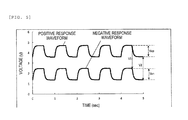
- FIG. 3 is a diagram depicting an example of a response waveform observed during normal operation, that is, when no leak occurs.
- FIGS. 4 and 5 depict examples of response waveforms observed during abnormal operation, that is, when a leak occurs.
- FIG. 4 is a diagram depicting an example of a response waveform observed when a leak occurs on the positive side
- FIG. 5 is a diagram depicting an example of a response waveform observed when a leak occurs on the negative side.
- examples of response waveforms observed when pulse signals each repeating ON (H level) and OFF (L level) every 0.5 minute are output to the positive connecting wire 21 and the negative connecting wire 22 as the positive pulse signal and the negative pulse signal, respectively, from the pulse signal outputting portion 201 .
- an upper waveform indicates a positive response waveform
- a lower waveform indicates a negative response waveform
- the amplitude of the positive response waveform is represented as Vap
- the amplitude of the negative response waveform is represented as Van
- the difference between the maximal value (maximum value) of the positive response waveform and the maximal value (maximum value) of the negative response waveform is represented as V 1
- the difference between the minimal value (minimum value) of the positive response waveform and the minimal value (minimum value) of the negative response waveform is represented as V 2 .
- a comparison of the response waveforms of FIGS. 3 to 5 reveals that, as compared to the response waveform of FIG. 3 observed when no leak occurs, in the response waveforms of FIGS. 4 and 5 observed when a leak occurs, the amplitude Vap of the positive response waveform and the amplitude Van of the negative response waveform are decreased.
- V 1 and V 2 described above, no change is observed between the response waveform of FIG. 3 observed when no leak occurs and the response waveforms of FIGS. 4 and 5 observed when a leak occurs. That is, when a leak occurs, only the amplitude changes in the positive response waveform and the negative response waveform, and the difference between them, that is, the potential difference between the positive connecting wire 21 and the negative connecting wire 22 does not change.
- the amplitude ratio calculating portion 203 calculates an amplitude ratio Rv by the following expression (1) based on the amplitude Vap of the positive response waveform and the amplitude Van of the negative response waveform depicted in the response waveforms of FIGS. 3 to 5 and the differences V 1 and V 2 .
- the calculated amplitude ratio Rv is sent to the leak detecting portion 204 from the amplitude ratio calculating portion 203 .
- Rv ( Vap+Van )/( V 1 +V 2) (1)
- the amplitude Vap of the positive response waveform and the amplitude Van of the negative response waveform are decreased as compared to those observed when no leak occurs.
- the differences V 1 and V 2 do not change. Therefore, it turns out that the amplitude ratio Rv calculated by the above-described expression (1) changes in response to the leak state between the batteries 1 and 2 and the chassis ground and becomes a smaller value when a leak occurs as compared to that observed during normal operation. By using this, it is possible to sense the presence or absence of a leak between the batteries 1 and 2 and the chassis ground based on the value of the amplitude ratio Rv in the leak detecting portion 204 .
- FIG. 6 is a flowchart depicting the flow of leak detection processing which is performed in the microcomputer 200 when the presence or absence of a leak is detected in the above-described manner.
- step S 10 the microcomputer 200 outputs, by the pulse signal outputting portion 201 , predetermined pulse signals as a positive pulse signal and a negative pulse signal.
- the positive pulse signal output from the pulse signal outputting portion 201 is output to the positive connecting wire 21 via the transistor circuit 101 , the PhotoMOS relay 103 , and the leak resistor 105 .
- the negative pulse signal output from the pulse signal outputting portion 201 is output to the negative connecting wire 22 via the transistor circuit 102 , the PhotoMOS relay 104 , and the leak resistor 106 .
- step S 20 the microcomputer 200 detects, by the response waveform detecting portion 202 , the response waveforms for the positive pulse signal and the negative pulse signal output in step S 10 as a positive response waveform and a negative response waveform.
- the positive response waveform is input to the A/D converter 210 from the positive connecting wire 21 via the voltage-dividing resistor portions 301 and the operational amplifier 303 and is detected in the response waveform detecting portion 202 .
- the negative response waveform is input to the A/D converter 210 from the negative connecting wire 22 via the voltage-dividing resistor portions 302 and the operational amplifier 304 and is detected in the response waveform detecting portion 202 .
- step S 30 the microcomputer 200 calculates, by the amplitude ratio calculating portion 203 , the amplitude Vap of the positive response waveform and the amplitude Van of the negative response waveform from the positive response waveform and the negative response waveform detected in step S 20 .
- the microcomputer 200 calculates, by the amplitude ratio calculating portion 203 , the amplitude Vap of the positive response waveform and the amplitude Van of the negative response waveform from the positive response waveform and the negative response waveform detected in step S 20 .
- the amplitude Vap of the positive response waveform and the amplitude Van of the negative response waveform may be determined.
- step S 40 the microcomputer 200 calculates, by the amplitude ratio calculating portion 203 , a difference V 1 between the maximal value (maximum value) of the positive response waveform and the maximal value (maximum value) of the negative response waveform and a difference V 2 between the minimal value (minimum value) of the positive response waveform and the minimal value (minimum value) of the negative response waveform based on the positive response waveform and the negative response waveform detected in step S 20 .
- the maximal value and the minimal value of the positive response waveform in each period and the maximal value and the minimal value of the negative response waveform in each period are determined and differences between them are calculated for each period. Then, by calculating the average value of the calculated differences of the periods, it is possible to calculate the above-described differences V 1 and V 2 .
- step S 30 and step S 40 may be performed at the same time in a series of processes without being performed separately.
- the maximal value (maximum value) and the minimal value (minimum value) of the positive response waveform and the maximal value (maximum value) and the minimal value (minimum value) of the negative response waveform are determined.
- the amplitude Vap of the positive response waveform is calculated from the difference between the maximal value (maximum value) and the minimal value (minimum value) of the positive response waveform
- the amplitude Van of the negative response waveform is calculated from the difference between the maximal value (maximum value) and the minimal value (minimum value) of the negative response waveform.
- the difference V 1 between the maximal value (maximum value) of the positive response waveform and the maximal value (maximum value) of the negative response waveform and the difference V 2 between the minimal value (minimum value) of the positive response waveform and the minimal value (minimum value) of the negative response waveform are calculated.
- the average value of each period may be calculated by using predetermined periods' worth positive response waveforms and negative response waveforms.
- step S 50 the microcomputer 200 calculates, by the amplitude ratio calculating portion 203 , the amplitude ratio Rv by using the above-described expression (1) based on the calculation results in steps S 30 and S 40 .
- step S 60 the microcomputer 200 compares, by the leak detecting portion 204 , the amplitude ratio Rv calculated in step S 50 with a predetermined threshold value Rth and determines whether or not the amplitude ratio Rv is less than the threshold value Rth.
- the threshold value Rth used for this determination is a value smaller than the amplitude ratio Rv during normal operation in which no leak occurs and is previously set in accordance with the response waveform observed when a leak occurs, the response waveform illustrated in FIGS. 4 and 5 .
- the procedure proceeds to step S 70 ; otherwise, the leak detection processing described in the flowchart of FIG. 6 is ended.
- step S 70 the microcomputer 200 detects, by the leak detecting portion 204 , a leak between the batteries 1 and 2 and the chassis ground.
- the positive side and the negative side of the batteries 1 and 2 are not differentiated from each other, and detection is performed on the assumption that a leak occurs between at least one of them and the chassis ground. Furthermore, at this time, a predetermined warning signal for notifying the user in the vehicle of the occurrence of a leak may be output.
- the microcomputer 200 ends the leak detection processing described in the flowchart of FIG. 6 .
- the leak detection device 100 outputs, by the pulse signal outputting portion 201 , predetermined pulse signals to the positive connecting wire 21 connected to the positive sides of the batteries 1 and 2 and to the negative connecting wire 22 connected to the negative sides of the batteries 1 and 2 (step S 10 ). Then, the leak detection device 100 detects, by the response waveform detecting portion 202 , a positive response waveform for the positive pulse signal output to the positive connecting wire 21 and a negative response waveform for the negative pulse signal output to the negative connecting wire 22 (step S 20 ).
- the leak detection device 100 calculates, by the amplitude ratio calculating portion 203 , an amplitude ratio based on this positive response waveform and negative response waveform (step S 50 ), and detects, by the leak detecting portion 204 , a leak between the batteries 1 and 2 and the chassis ground based on the calculated amplitude ratio (steps S 60 and S 70 ). By doing so, even when the battery voltage varies, it is possible to detect the presence or absence of a leak correctly.
- the amplitude ratio calculating portion 203 calculates, in step S 50 , the amplitude ratio Rv by the above-described expression (1) based on the amplitude Vap of the positive response waveform and the amplitude Van of the negative response waveform calculated in step S 30 and the difference V 1 between the maximal value of the positive response waveform and the maximal value of the negative response waveform and the difference V 2 between the minimal value of the positive response waveform and the minimal value of the negative response waveform, the differences V 1 and V 2 calculated in step S 40 .
- the positive response waveform and the negative response waveform it is possible to calculate the amplitude ratio in accordance with the leak state between the batteries 1 and 2 and the chassis ground.
- the leak detecting portion 204 determines whether or not the amplitude ratio Rv is less than the predetermined threshold value Rth in step S 60 , and, when the amplitude ratio Rv becomes less than the threshold value Rth, in step S 70 , the leak detecting portion 204 detects a leak between at least one of the positive and negative sides of the batteries 1 and 2 and the chassis ground. By doing so, it is possible to detect the occurrence of a leak easily and reliably.
- the leak detection device 100 includes the PhotoMOS relays 103 and 104 as insulating circuits that provide insulation between the positive connecting wire 21 and the pulse signal outputting portion 201 and between the negative connecting wire 22 and the pulse signal outputting portion 201 .
- the pulse signal outputting portion 201 outputs pulse signals to the positive connecting wire 21 and the negative connecting wire 22 via the PhotoMOS relays 103 and 104 , respectively. By doing so, irrespective of the potential difference between the microcomputer 200 having the pulse signal outputting portion 201 and the positive connecting wire 21 and the negative connecting wire 22 , it is possible to output the pulse signals to the positive connecting wire 21 and the negative connecting wire 22 from the pulse signal outputting portion 201 .
- the insulating circuits are configured by using the PhotoMOS relays 103 and 104 , even when the high-voltage batteries 1 and 2 are used, it is possible to provide proper insulation between the positive connecting wire 21 and the pulse signal outputting portion 201 and between the negative connecting wire 22 and the pulse signal outputting portion 201 .
- the leak detection device 100 includes the voltage-dividing resistor portions 301 and 302 that divide the voltage of the positive connecting wire 21 and the voltage of the negative connecting wire 22 , respectively.
- the response waveform detecting portion 202 detects the positive response waveform and the negative response waveform via the voltage-dividing resistor portions 301 and 302 . By doing so, it is possible to detect the positive response waveform and the negative response waveform within an appropriate voltage range.
- the leak detection device that detects a leak based on the response waveform observed when the pulse signals are input to the positive and negative sides of the connecting wires between the batteries and the chassis ground has been described.
- the second embodiment which will be described below, a leak detection device that performs detection of the state of an insulating circuit used for input of a pulse signal in addition to leak detection similar to that described in the first embodiment will be described.
- FIG. 7 is a diagram depicting the configuration of a leak detection device 100 a according to this embodiment.
- the leak detection device 100 a depicted in FIG. 7 differs from the leak detection device 100 according to the first embodiment depicted in FIG. 2 in that a monitor waveform detecting portion 205 and an insulation diagnosing portion 206 are further provided in the microcomputer 200 and voltage-dividing circuits 107 and 108 are connected to the PhotoMOS relays 103 and 104 , respectively.
- a power supply device including this leak detection device 100 a has the same configuration as the power supply device depicted in FIG. 1 , the power supply device including the leak detection device 100 .
- the voltage-dividing circuits 107 and 108 are connected between the PhotoMOSFETs on the output sides of the PhotoMOS relays 103 and 104 and the control ground, respectively. Then, the voltage-dividing circuits 107 and 108 divide the output voltages of the PhotoMOS relays 103 and 104 at the time of output of the positive pulse signal and the negative pulse signal to the positive connecting wire 21 and the negative connecting wire 22 from the pulse signal outputting portion 201 via the PhotoMOS relays 103 and 104 , respectively, at predetermined voltage-dividing ratios and output the resultant voltages. The waveforms of these output voltages are output to the monitor waveform detecting portion 205 of the microcomputer 200 from the voltage-dividing circuits 107 and 108 as a positive monitor waveform and a negative monitor waveform.
- the monitor waveform detecting portion 205 incorporates an A/D converter 211 and takes in the positive monitor waveform and the negative monitor waveform input from the voltage-dividing circuits 107 and 108 as digital values, respectively, by using this A/D converter 211 .
- the monitor waveform detecting portion 205 it is possible to detect the positive monitor waveform and the negative monitor waveform at the time of output of the positive pulse signal and the negative pulse signal.
- the insulation diagnosing portion 206 makes a diagnosis as to whether the states of the PhotoMOS relays 103 and 104 are normal or abnormal states such as a short-circuit state and an open state based on the positive monitor waveform and the negative monitor waveform detected by the monitor waveform detecting portion 205 .
- a specific method for making a diagnosis of the states of the PhotoMOS relays 103 and 104 by the insulation diagnosing portion 206 will be described in detail later.
- monitor waveforms which will be detected when the PhotoMOS relays 103 and 104 are brought into a short-circuit state will be described. For example, if the PhotoMOS relay 103 is brought into a short-circuit state due to a breakdown or the like, irrespective of the presence or absence of an output of the positive pulse signal from the pulse signal outputting portion 201 , the state enters a state in which the positive connecting wire 21 and the negative connecting wire 22 are always connected to the control ground.
- FIG. 8 is a diagram depicting an example of a response waveform observed when a leak occurs on the positive side in a normal state of the PhotoMOS relay 103 .
- FIG. 9 is a diagram depicting an example of a response waveform observed when no leak occurs in a short-circuit state of the PhotoMOS relay 103 .
- FIG. 10 is a diagram depicting an example of a response waveform observed when no leak occurs in a normal state of the PhotoMOS relay 103 , and is similar to the response waveform observed when no leak occurs in the first embodiment depicted in FIG. 3 .
- the positive monitor waveform and the negative monitor waveform output from the voltage-dividing circuits 107 and 108 are detected by the monitor waveform detecting portion 205 , and a diagnosis as to whether or not the PhotoMOS relays 103 and 104 which are insulating circuits are in the normal state is made by the insulation diagnosing portion 206 based on these waveforms.
- Use of this diagnosis result with the result of detection of the leak state based on the response waveform described in the first embodiment makes it possible to detect the presence or absence of a leak in the positive connecting wire 21 and the negative connecting wire 22 correctly.
- FIG. 11 is a diagram depicting an example of a monitor waveform observed when the PhotoMOS relay 103 on the positive side is short-circuited
- FIG. 12 is a diagram depicting an example of a monitor waveform observed when the PhotoMOS relay 104 on the negative side is short-circuited
- FIG. 13 is a diagram depicting an example of a monitor waveform observed when the PhotoMOS relays 103 and 104 are normal.
- the waveform indicated by a solid line represents a positive monitor waveform in response to ON/OFF of a positive pulse signal
- the waveform indicated by a broken line represents a negative monitor waveform in response to ON/OFF of a negative pulse signal.
- “ON” and “OFF” depicted in an upper stage indicate ON/OFF timing of a positive pulse signal
- “ON” and “OFF” depicted in a lower stage indicate ON/OFF timing of a negative pulse signal.
- Vmp 1 and Vmn 1 represent the voltages of the positive monitor waveform and the negative monitor waveform, respectively, at the first reference point.
- Vmp 2 and Vmn 2 represent the positive monitor waveform and the negative monitor waveform, respectively, at the second reference point.
- the insulation diagnosing portion 206 calculates a voltage difference Vm 1 between the positive monitor waveform and the negative monitor waveform at the first reference point by the following expression (2) based on the voltages Vmp 1 and Vmn 1 depicted in the monitor waveforms of FIGS. 11 to 13 .
- Vm 1 Vmp 1 ⁇ Vmn 1 (2)
- a voltage difference Vm 2 between the positive monitor waveform and the negative monitor waveform at the second reference point is calculated by the following expression (3) based on the voltages Vmp 2 and Vmn 2 depicted in the monitor waveforms of FIGS. 11 to 13 .
- Vm 2 Vmp 2 ⁇ Vmn 2 (3)
- Vd Vmp 2 ⁇ Vmn 1 (4)
- the insulation diagnosing portion 206 calculates indexes for making a diagnosis as to whether or not the PhotoMOS relays 103 and 104 are in a normal state based on the voltage differences determined by the above-described expressions (2) to (4). Specifically, based on the voltage differences Vm 1 , Vm 2 , and Vd of the expressions (2) to (4) and the difference V 1 between the maximal value of the positive response waveform and the maximal value of the negative response waveform and the difference V 2 between the minimal value of the positive response waveform and the minimal value of the negative response waveform described in the above-described first embodiment, by the following expressions (5) to (7), a first monitor ratio Am 1 , a second monitor ratio Am 2 , and a monitor difference ratio Ad as diagnosis indexes are calculated.
- the insulation diagnosing portion 206 After calculating the first monitor ratio Am 1 , the second monitor ratio Am 2 , and the monitor difference ratio Ad in the manner described above, the insulation diagnosing portion 206 makes a diagnosis of the states of the PhotoMOS relays 103 and 104 by comparing these diagnosis indexes with predetermined threshold values. For example, if the second monitor ratio Am 2 and the monitor difference ratio Ad satisfy the following conditional expression (8), the insulation diagnosing portion 206 determines that the PhotoMOS relay 103 is short-circuited.
- Tha and Thb are threshold values which are previously set as data set values of software. Am 2 ⁇ Tha and Ad ⁇ Thb (8)
- the insulation diagnosing portion 206 determines that the PhotoMOS relay 104 is short-circuited.
- the and Thd are threshold values which are previously set as data set values of software.
- the values of these threshold values Thc and Thd may be the same as or different from the threshold values Tha and Thb in the conditional expression (8) described above.
- the insulation diagnosing portion 206 determines that at least one of the PhotoMOS relays 103 and 104 is in an open state and the positive pulse signal or the negative pulse signal is interrupted in the PhotoMOS relay 103 or 104 .
- The, Thf, and Thg are threshold values which are previously set as data set values of software. The values of these threshold values The, Thf, and Thg may be the same as or different from the threshold values Tha and Thb in the conditional expression (8) described above and the threshold values Thc and Thd in the conditional expression (9) described above.
- FIG. 14 is a flowchart depicting the flow of leak and relay state detection processing which is performed in the microcomputer 200 when the presence or absence of a leak is detected and a diagnosis of the states of the PhotoMOS relays 103 and 104 is made in the manner described above.
- FIG. 14 portions performing the same processing as the leak detection processing of the first embodiment depicted in FIG. 6 are identified with the same step numbers as those of FIG. 6 .
- steps S 10 to S 70 the microcomputer 200 performs leak detection processing by performing the processing similar to that of FIG. 6 .
- step S 80 the microcomputer 200 detects, by the monitor waveform detecting portion 205 , the output voltage waveforms of the PhotoMOS relays 103 and 104 observed when the positive pulse signal and the negative pulse signal are output in step S 10 as a positive monitor waveform and a negative monitor waveform.
- the positive monitor waveform is input to the A/D converter 211 via the voltage-dividing circuit 107 from the PhotoMOS relay 103 and is detected in the monitor waveform detecting portion 205 .
- the negative monitor waveform is input to the A/D converter 211 via the voltage-dividing circuit 108 from the PhotoMOS relay 104 and is detected in the monitor waveform detecting portion 205 .
- step S 90 the microcomputer 200 determines, by the insulation diagnosing portion 206 , the voltage Vmp 1 of the positive monitor waveform and the voltage Vmn 1 of the negative monitor waveform at the above-described first reference point and the voltage Vmp 2 of the positive monitor waveform and the voltage Vmn 2 of the negative monitor waveform at the second reference point from the positive monitor waveform and the negative monitor waveform detected in step S 80 .
- the microcomputer 200 calculates the voltage difference Vm 1 between the positive monitor waveform and the negative monitor waveform at the first reference point, the voltage difference Vm 2 between the positive monitor waveform and the negative monitor waveform at the second reference point, and the voltage difference Vd at the rising start point of the positive monitor waveform and the negative monitor waveform by using the above-described expressions (2) to (4).
- step S 100 the microcomputer 200 calculates, by the insulation diagnosing portion 206 , the first monitor ratio Am1, the second monitor ratio Am 2 , and the monitor difference ratio Ad by the above-described expressions (5) to (7) based on the voltage differences Vm 1 , Vm 2 , and Vd calculated in step S 90 and the differences V 1 and V 2 calculated in step S 40 .
- step S 110 the microcomputer 200 determines, by the insulation diagnosing portion 206 , whether or not the second monitor ratio Am 2 and the monitor difference ratio Ad calculated in step S 100 satisfy the conditional expression (8) described above by comparing the second monitor ratio Am 2 and the monitor difference ratio Ad with the predetermined threshold values Tha and Thb, respectively.
- the procedure proceeds to step S 120 ; if the second monitor ratio Am 2 and the monitor difference ratio Ad do not satisfy the conditional expression (8), the procedure proceeds to step S 130 .
- step S 120 the microcomputer 200 determines, by the insulation diagnosing portion 206 , that the PhotoMOS relay 103 between the positive connecting wire 21 and the pulse signal outputting portion 201 is short-circuited and detects a short-circuit in the PhotoMOS relay 103 . At this time, a predetermined warning signal or the like may be output to notify the user in the vehicle that the PhotoMOS relay 103 is short-circuited.
- step S 130 the microcomputer 200 determines, by the insulation diagnosing portion 206 , whether or not the first monitor ratio Am 1 and the monitor difference ratio Ad calculated in step S 100 satisfy the conditional expression (9) described above by comparing the first monitor ratio Am 1 and the monitor difference ratio Ad with the predetermined threshold values Thc and Thd, respectively.
- the procedure proceeds to step S 140 ; if the first monitor ratio Am 1 and the monitor difference ratio Ad do not satisfy the conditional expression (9), the procedure proceeds to step S 150 .
- step S 140 the microcomputer 200 determines, by the insulation diagnosing portion 206 , that the PhotoMOS relay 104 between the negative connecting wire 22 and the pulse signal outputting portion 201 is short-circuited and detects a short-circuit in the PhotoMOS relay 104 . At this time, a predetermined warning signal or the like may be output to notify the user in the vehicle that the PhotoMOS relay 104 is short-circuited.
- step S 150 the microcomputer 200 determines, by the insulation diagnosing portion 206 , whether or not the first monitor ratio Am 1 and the first monitor ratio Am 1 calculated in step S 100 and the amplitude ratio Rv calculated in step S 50 satisfy the conditional expression (10) described above by comparing the first monitor ratio Am 1 , the second monitor ratio Am 2 , and the amplitude ratio Rv with the predetermined threshold values The, Thf, and Thg, respectively.
- the procedure proceeds to step S 160 ; if the first monitor ratio Am 1 , the first monitor ratio Am 1 , and the amplitude ratio Rv do not satisfy the conditional expression (10), the processing described in the flowchart of FIG. 14 is ended.
- step S 160 the microcomputer 200 determines, by the insulation diagnosing portion 206 , that at least one of the PhotoMOS relays 103 and 104 interrupts a pulse signal from the pulse signal outputting portion 201 and detects that these relays are in an open state. At this time, a predetermined warning signal or the like may be output to notify the user in the vehicle that the PhotoMOS relay 103 or 104 is in an open state.
- the microcomputer 200 ends the processing described in the flowchart of FIG. 14 .
- the leak detection device 100 a includes the monitor waveform detecting portion 205 and the insulation diagnosing portion 206 in the microcomputer 200 .
- the monitor waveform detecting portion 205 detects, as a positive monitor waveform and a negative monitor waveform, the output voltage waveforms of the PhotoMOS relays 103 and 104 observed when the pulse signals are output to the positive connecting wire 21 and the negative connecting wire 22 via the PhotoMOS relays 103 and 104 as the insulating circuits from the pulse signal outputting portion 201 (step S 80 ).
- the insulation diagnosing portion 206 makes a diagnosis of the states of the PhotoMOS relays 103 and 104 based on the positive monitor waveform and the negative monitor waveform detected by the monitor waveform detecting portion 205 (steps S 90 to S 160 ). By doing so, it is possible to detect the presence or absence of a leak in the positive connecting wire 21 and the negative connecting wire 22 with consideration given to the states of the PhotoMOS relays 103 and 104 .
- the pulse signal outputting portion 201 alternately outputs a positive pulse signal to the positive connecting wire 21 and a negative pulse signal to the negative connecting wire 22 .
- the insulation diagnosing portion 206 calculates, in step S 90 , the voltage Vmp 1 of the positive monitor waveform and the voltage Vmn 1 of the negative monitor waveform at the first reference point corresponding to the falling start point of the positive pulse signal and the rising start point of the negative pulse signal and the voltage Vmp 2 of the positive monitor waveform and the voltage Vmn 2 of the negative monitor waveform at the second reference point corresponding to the rising start point of the positive pulse signal and the falling start point of the negative pulse signal.
- the first monitor ratio Am 1 , the second monitor ratio Am 2 , and the monitor difference ratio Ad are calculated.
- steps S 110 to S 160 based on the first monitor ratio Am 1 , the second monitor ratio Am 2 , and the monitor difference ratio Ad thus calculated, a diagnosis of the states of the PhotoMOS relays 103 and 104 is made. By doing so, it is possible to make a diagnosis of the states of the PhotoMOS relays 103 and 104 accurately.
- the insulation diagnosing portion 206 determines that the PhotoMOS relay 103 between the positive connecting wire 21 and the pulse signal outputting portion 201 is short-circuited when the second monitor ratio Am 2 is more than or equal to the predetermined threshold value Tha and the monitor difference ratio Ad becomes more than or equal to the predetermined threshold value Thb in steps S 110 and S 120 . Moreover, the insulation diagnosing portion 206 determines that the PhotoMOS relay 104 between the negative connecting wire 22 and the pulse signal outputting portion 201 is short-circuited when the first monitor ratio Am 1 is more than or equal to the predetermined threshold value The and the monitor difference ratio Ad becomes more than or equal to the predetermined threshold value Thd in steps S 130 and S 140 . By doing so, it is possible to determine reliably whether or not the PhotoMOS relays 103 and 104 are short-circuited.
- the insulation diagnosing portion 206 determines that the PhotoMOS relay 103 or 104 interrupts the pulse signal when both the first monitor ratio Am 1 and the second monitor ratio Am 2 are less than or equal to the predetermined threshold values
- the and Thf and the amplitude ratio Rv calculated by the amplitude ratio calculating portion 203 becomes less than or equal to the predetermined threshold value Thg in steps S 150 and S 160 . By doing so, it is possible to determine reliably whether or not the PhotoMOS relays 103 and 104 are in an open state.
- the leak detection device 100 a further includes the voltage-dividing circuits 107 and 108 connected to the output sides of the PhotoMOS relays 103 and 104 .
- the monitor waveform detecting portion 205 detects the positive monitor waveform and the negative monitor waveform via the voltage-dividing circuits 107 and 108 . By doing so, it is possible to detect the positive monitor waveform and the negative monitor waveform within an appropriate voltage range in the monitor waveform detecting portion 205 .
- a leak detection device that inputs pulse signals to a positive connecting wire and a negative connecting wire via insulating circuits and performs leak detection based on shape variations in response waveforms for the pulse signals, it is possible to make a diagnosis of the states of the insulating circuits by applying the method for making a diagnosis of an insulating circuit, the method described in the second embodiment, to the leak detection device.
Landscapes
- Engineering & Computer Science (AREA)
- Power Engineering (AREA)
- Transportation (AREA)
- Mechanical Engineering (AREA)
- Life Sciences & Earth Sciences (AREA)
- Sustainable Development (AREA)
- Sustainable Energy (AREA)
- Physics & Mathematics (AREA)
- General Physics & Mathematics (AREA)
- Testing Of Short-Circuits, Discontinuities, Leakage, Or Incorrect Line Connections (AREA)
Abstract
Description
Rv=(Vap+Van)/(V1+V2) (1)
Vm1=Vmp1−Vmn1 (2)
Vm2=Vmp2−Vmn2 (3)
Vd=Vmp2−Vmn1 (4)
Am2≥Tha and Ad≥Thb (8)
Am1≥Thc and Ad≥Thd (9)
Am1≤The and Am2≤Thf and Rv≤Thg (10)
Claims (13)
Rv=(Vap+Van)/(V1+V2);
AM1=2(Vmp1−Vmn1)/(V1+V2)
AM2=2(Vmp2−Vmn2)/(V1+V2)
Ad=2(Vmp2−Vmn1)/(V1+V2),
AM1=2(Vmp1−Vmn1)/(V1+V2)
Am2=2(Vmp2−Vmn2)/(V1+V2)
Ad=2(Vmp2−Vmn1)/(V1+V2),
Applications Claiming Priority (4)
| Application Number | Priority Date | Filing Date | Title |
|---|---|---|---|
| WOPCT/JP2012/065478 | 2012-06-18 | ||
| JPPCT/JP2012/065478 | 2012-06-18 | ||
| PCT/JP2012/065478 WO2013190611A1 (en) | 2012-06-18 | 2012-06-18 | Leak detecting apparatus |
| PCT/JP2012/084147 WO2013190733A1 (en) | 2012-06-18 | 2012-12-28 | Leak detection device |
Publications (2)
| Publication Number | Publication Date |
|---|---|
| US20150168474A1 US20150168474A1 (en) | 2015-06-18 |
| US10073128B2 true US10073128B2 (en) | 2018-09-11 |
Family
ID=49768242
Family Applications (1)
| Application Number | Title | Priority Date | Filing Date |
|---|---|---|---|
| US14/409,184 Active 2035-05-28 US10073128B2 (en) | 2012-06-18 | 2012-12-28 | Leak detection device |
Country Status (4)
| Country | Link |
|---|---|
| US (1) | US10073128B2 (en) |
| EP (1) | EP2866038B1 (en) |
| CN (1) | CN104380123B (en) |
| WO (2) | WO2013190611A1 (en) |
Cited By (5)
| Publication number | Priority date | Publication date | Assignee | Title |
|---|---|---|---|---|
| US20220360091A1 (en) * | 2021-05-04 | 2022-11-10 | Exro Technologies Inc. | Battery Control Systems and Methods |
| US11539222B2 (en) * | 2019-04-04 | 2022-12-27 | Yazaki Corporation | Battery control unit and battery system |
| US20220413061A1 (en) * | 2019-11-26 | 2022-12-29 | Sanyo Electric Co., Ltd. | Earth leakage detecting device, and vehicular power supply system |
| US11722026B2 (en) | 2019-04-23 | 2023-08-08 | Dpm Technologies Inc. | Fault tolerant rotating electric machine |
| US11967913B2 (en) | 2021-05-13 | 2024-04-23 | Exro Technologies Inc. | Method and apparatus to drive coils of a multiphase electric machine |
Families Citing this family (13)
| Publication number | Priority date | Publication date | Assignee | Title |
|---|---|---|---|---|
| US9496200B2 (en) | 2011-07-27 | 2016-11-15 | Coolit Systems, Inc. | Modular heat-transfer systems |
| US10365667B2 (en) * | 2011-08-11 | 2019-07-30 | Coolit Systems, Inc. | Flow-path controllers and related systems |
| WO2014141162A1 (en) * | 2013-03-15 | 2014-09-18 | Coolit Systems, Inc. | Sensors, multiplexed communication techniques, and related systems |
| JP5518138B2 (en) * | 2012-07-09 | 2014-06-11 | 本田技研工業株式会社 | Non-grounded circuit ground fault detector |
| US9440601B2 (en) * | 2013-09-06 | 2016-09-13 | Johnson Controls Technology Company | System for providing voltage measurements of battery cells to a PCB within a battery module |
| US10725115B2 (en) * | 2014-10-16 | 2020-07-28 | Ford Global Technologies, Llc | Methods and apparatus for detecting electrical leakage in a vehicle |
| CN107539149B (en) * | 2017-08-29 | 2020-02-14 | 宁德时代新能源科技股份有限公司 | Control circuit, battery system and vehicle |
| US11452243B2 (en) | 2017-10-12 | 2022-09-20 | Coolit Systems, Inc. | Cooling system, controllers and methods |
| TWI725422B (en) * | 2018-05-31 | 2021-04-21 | 技嘉科技股份有限公司 | Liquid cooling device, coolant circulation system , and liquid leaking detection method |
| US11662037B2 (en) | 2019-01-18 | 2023-05-30 | Coolit Systems, Inc. | Fluid flow control valve for fluid flow systems, and methods |
| US11473860B2 (en) | 2019-04-25 | 2022-10-18 | Coolit Systems, Inc. | Cooling module with leak detector and related systems |
| US11395443B2 (en) | 2020-05-11 | 2022-07-19 | Coolit Systems, Inc. | Liquid pumping units, and related systems and methods |
| US11725886B2 (en) | 2021-05-20 | 2023-08-15 | Coolit Systems, Inc. | Modular fluid heat exchange systems |
Citations (12)
| Publication number | Priority date | Publication date | Assignee | Title |
|---|---|---|---|---|
| JPS60183565A (en) | 1984-03-01 | 1985-09-19 | Kansai Electric Power Co Inc:The | Flicker type direct current grounding point searcher |
| US4893085A (en) * | 1988-03-18 | 1990-01-09 | Mitsubishi Denki Kabushiki Kaisha | Ignition monitoring circuit for an ignition system of an internal combustion engine including an erroneous pulse eliminating circuit means |
| US6778913B2 (en) | 2002-04-29 | 2004-08-17 | Cadex Electronics Inc. | Multiple model systems and methods for testing electrochemical systems |
| US20040243288A1 (en) | 2003-05-29 | 2004-12-02 | Yuji Kito | Diagnostic system and method for electric leak detecting device |
| JP2005189005A (en) | 2003-12-24 | 2005-07-14 | Honda Motor Co Ltd | Ground fault detection system |
| JP2006145293A (en) | 2004-11-17 | 2006-06-08 | Daihatsu Motor Co Ltd | Short-circuit detector |
| US20070008666A1 (en) | 2005-07-11 | 2007-01-11 | Nissan Motor Co., Ltd. | Ground fault detector for vehicle |
| JP2010019603A (en) | 2008-07-08 | 2010-01-28 | Hitachi Ltd | Power supply |
| WO2010109956A1 (en) * | 2009-03-27 | 2010-09-30 | 株式会社日立製作所 | Electric storage device |
| JP2010249766A (en) | 2009-04-20 | 2010-11-04 | Hitachi Ltd | Vehicular leakage detection device |
| US20110215793A1 (en) * | 2008-01-11 | 2011-09-08 | Mitsubishi Heavy Industries, Ltd. | Method and device for diagnosing signal status in measurement, drive, or control, and transformer used in the device |
| US20120043967A1 (en) | 2009-09-29 | 2012-02-23 | Hitachi Vehicle Energy, Ltd. | Ground Fault Detection Circuit, and Power Supply Device |
Family Cites Families (4)
| Publication number | Priority date | Publication date | Assignee | Title |
|---|---|---|---|---|
| JPH10221395A (en) * | 1997-02-07 | 1998-08-21 | Denso Corp | System for detecting ground fault of electric vehicle |
| AU2008280932B8 (en) * | 2007-07-24 | 2011-02-24 | Panasonic Electric Works Co., Ltd. | Charging monitor |
| CN201886117U (en) * | 2010-09-29 | 2011-06-29 | 京滨电子装置研究开发(上海)有限公司 | Insulation detection circuit of electrically-propelled vehicle |
| JP5710307B2 (en) * | 2011-02-16 | 2015-04-30 | オムロンオートモーティブエレクトロニクス株式会社 | Earth leakage detector |
-
2012
- 2012-06-18 WO PCT/JP2012/065478 patent/WO2013190611A1/en active Application Filing
- 2012-12-28 CN CN201280074079.1A patent/CN104380123B/en active Active
- 2012-12-28 EP EP12879186.0A patent/EP2866038B1/en active Active
- 2012-12-28 WO PCT/JP2012/084147 patent/WO2013190733A1/en active Application Filing
- 2012-12-28 US US14/409,184 patent/US10073128B2/en active Active
Patent Citations (14)
| Publication number | Priority date | Publication date | Assignee | Title |
|---|---|---|---|---|
| JPS60183565A (en) | 1984-03-01 | 1985-09-19 | Kansai Electric Power Co Inc:The | Flicker type direct current grounding point searcher |
| US4893085A (en) * | 1988-03-18 | 1990-01-09 | Mitsubishi Denki Kabushiki Kaisha | Ignition monitoring circuit for an ignition system of an internal combustion engine including an erroneous pulse eliminating circuit means |
| US6778913B2 (en) | 2002-04-29 | 2004-08-17 | Cadex Electronics Inc. | Multiple model systems and methods for testing electrochemical systems |
| US20040243288A1 (en) | 2003-05-29 | 2004-12-02 | Yuji Kito | Diagnostic system and method for electric leak detecting device |
| JP2005189005A (en) | 2003-12-24 | 2005-07-14 | Honda Motor Co Ltd | Ground fault detection system |
| JP2006145293A (en) | 2004-11-17 | 2006-06-08 | Daihatsu Motor Co Ltd | Short-circuit detector |
| US20070008666A1 (en) | 2005-07-11 | 2007-01-11 | Nissan Motor Co., Ltd. | Ground fault detector for vehicle |
| US20110215793A1 (en) * | 2008-01-11 | 2011-09-08 | Mitsubishi Heavy Industries, Ltd. | Method and device for diagnosing signal status in measurement, drive, or control, and transformer used in the device |
| JP2010019603A (en) | 2008-07-08 | 2010-01-28 | Hitachi Ltd | Power supply |
| WO2010109956A1 (en) * | 2009-03-27 | 2010-09-30 | 株式会社日立製作所 | Electric storage device |
| US20110313613A1 (en) * | 2009-03-27 | 2011-12-22 | Hitachi Vechicle Energy, Ltd. | Electric Storage Device |
| JPWO2010109956A1 (en) * | 2009-03-27 | 2012-09-27 | 株式会社日立製作所 | Power storage device |
| JP2010249766A (en) | 2009-04-20 | 2010-11-04 | Hitachi Ltd | Vehicular leakage detection device |
| US20120043967A1 (en) | 2009-09-29 | 2012-02-23 | Hitachi Vehicle Energy, Ltd. | Ground Fault Detection Circuit, and Power Supply Device |
Non-Patent Citations (1)
| Title |
|---|
| The Extended European Search Report dated Mar. 8, 2016 in the EP Application No. 12879186.0. |
Cited By (8)
| Publication number | Priority date | Publication date | Assignee | Title |
|---|---|---|---|---|
| US11539222B2 (en) * | 2019-04-04 | 2022-12-27 | Yazaki Corporation | Battery control unit and battery system |
| US11722026B2 (en) | 2019-04-23 | 2023-08-08 | Dpm Technologies Inc. | Fault tolerant rotating electric machine |
| US20220413061A1 (en) * | 2019-11-26 | 2022-12-29 | Sanyo Electric Co., Ltd. | Earth leakage detecting device, and vehicular power supply system |
| US20220360091A1 (en) * | 2021-05-04 | 2022-11-10 | Exro Technologies Inc. | Battery Control Systems and Methods |
| US20220368135A1 (en) * | 2021-05-04 | 2022-11-17 | Exro Technologies Inc. | Battery Control Systems and Methods |
| US11708005B2 (en) * | 2021-05-04 | 2023-07-25 | Exro Technologies Inc. | Systems and methods for individual control of a plurality of battery cells |
| US11897362B2 (en) * | 2021-05-04 | 2024-02-13 | Exro Technologies Inc. | Systems and methods for individual control of a plurality of controllable units of battery cells |
| US11967913B2 (en) | 2021-05-13 | 2024-04-23 | Exro Technologies Inc. | Method and apparatus to drive coils of a multiphase electric machine |
Also Published As
| Publication number | Publication date |
|---|---|
| WO2013190733A1 (en) | 2013-12-27 |
| US20150168474A1 (en) | 2015-06-18 |
| EP2866038A1 (en) | 2015-04-29 |
| WO2013190611A1 (en) | 2013-12-27 |
| EP2866038B1 (en) | 2018-09-12 |
| EP2866038A4 (en) | 2016-07-06 |
| CN104380123A (en) | 2015-02-25 |
| CN104380123B (en) | 2016-12-14 |
Similar Documents
| Publication | Publication Date | Title |
|---|---|---|
| US10073128B2 (en) | Leak detection device | |
| US10017071B2 (en) | Method and system for diagnosing contactor health in a high-voltage electrical system | |
| CN112513651B (en) | Method for detecting insulation faults | |
| US10534032B2 (en) | Insulation resistance measuring system and device | |
| US7852089B2 (en) | Ground-fault detection system for vehicles with a high-voltage power net | |
| CN111090027B (en) | High voltage system and method for monitoring an insulation fault in a high voltage system | |
| US20140049860A1 (en) | Earth fault detection circuit and power source device | |
| JP4874034B2 (en) | Battery pack for electric vehicles | |
| JP2007198995A (en) | Ground fault resistance measurement circuit and ground fault detection circuit | |
| US9694686B2 (en) | Multifunctional monitoring of electrical systems | |
| US11906599B2 (en) | Earth leakage detecting device, and vehicular power supply system | |
| US9941815B2 (en) | Power conversion apparatus with overcurrent simulating circuit | |
| US10972017B2 (en) | Control unit for controlling an inverter, inverter and method for operating an inverter | |
| KR102291762B1 (en) | Circuit for diagnosing a relay | |
| CN104483588B (en) | The electric fault diagnosis method and apparatus at Control end | |
| EP3509178A1 (en) | Diagnostic system for vehicle electrical system having dc-dc voltage converter and voltage regulator | |
| US20220413061A1 (en) | Earth leakage detecting device, and vehicular power supply system | |
| CN105896940A (en) | Power conversion apparatus | |
| JP2013240238A (en) | Power conversion device | |
| JP5748610B2 (en) | Charger | |
| US20230152375A1 (en) | Deterioration estimation device and deterioration estimation program for power conversion device | |
| JP4123441B2 (en) | Inrush current limiting power switch circuit for vehicles | |
| JP5926796B2 (en) | Leak detector | |
| JP6287218B2 (en) | Anomaly detection device | |
| US10615682B2 (en) | Electrically driven vehicle inverter device |
Legal Events
| Date | Code | Title | Description |
|---|---|---|---|
| AS | Assignment |
Owner name: HITACHI AUTOMOTIVE SYSTEMS, LTD., JAPAN Free format text: ASSIGNMENT OF ASSIGNORS INTEREST;ASSIGNORS:YOSHIOKA, YUJI;KAI, TSUYOSHI;KUDO, AKIHIKO;AND OTHERS;REEL/FRAME:034549/0398 Effective date: 20141028 |
|
| STCF | Information on status: patent grant |
Free format text: PATENTED CASE |
|
| AS | Assignment |
Owner name: HITACHI ASTEMO, LTD., JAPAN Free format text: CHANGE OF NAME;ASSIGNOR:HITACHI AUTOMOTIVE SYSTEMS, LTD.;REEL/FRAME:056299/0447 Effective date: 20210101 |
|
| MAFP | Maintenance fee payment |
Free format text: PAYMENT OF MAINTENANCE FEE, 4TH YEAR, LARGE ENTITY (ORIGINAL EVENT CODE: M1551); ENTITY STATUS OF PATENT OWNER: LARGE ENTITY Year of fee payment: 4 |