US10056458B2 - Siloxane and organic-based MOL contact patterning - Google Patents
Siloxane and organic-based MOL contact patterning Download PDFInfo
- Publication number
- US10056458B2 US10056458B2 US14/993,537 US201614993537A US10056458B2 US 10056458 B2 US10056458 B2 US 10056458B2 US 201614993537 A US201614993537 A US 201614993537A US 10056458 B2 US10056458 B2 US 10056458B2
- Authority
- US
- United States
- Prior art keywords
- layer
- sog
- forming
- over
- barc
- Prior art date
- Legal status (The legal status is an assumption and is not a legal conclusion. Google has not performed a legal analysis and makes no representation as to the accuracy of the status listed.)
- Active, expires
Links
Images


Classifications
-
- H01L29/401—
-
- H—ELECTRICITY
- H10—SEMICONDUCTOR DEVICES; ELECTRIC SOLID-STATE DEVICES NOT OTHERWISE PROVIDED FOR
- H10D—INORGANIC ELECTRIC SEMICONDUCTOR DEVICES
- H10D64/00—Electrodes of devices having potential barriers
- H10D64/01—Manufacture or treatment
-
- H01L21/02126—
-
- H01L21/02282—
-
- H01L21/28229—
-
- H01L29/41791—
-
- H01L29/4232—
-
- H—ELECTRICITY
- H10—SEMICONDUCTOR DEVICES; ELECTRIC SOLID-STATE DEVICES NOT OTHERWISE PROVIDED FOR
- H10D—INORGANIC ELECTRIC SEMICONDUCTOR DEVICES
- H10D30/00—Field-effect transistors [FET]
- H10D30/60—Insulated-gate field-effect transistors [IGFET]
-
- H—ELECTRICITY
- H10—SEMICONDUCTOR DEVICES; ELECTRIC SOLID-STATE DEVICES NOT OTHERWISE PROVIDED FOR
- H10D—INORGANIC ELECTRIC SEMICONDUCTOR DEVICES
- H10D30/00—Field-effect transistors [FET]
- H10D30/60—Insulated-gate field-effect transistors [IGFET]
- H10D30/62—Fin field-effect transistors [FinFET]
- H10D30/6219—Fin field-effect transistors [FinFET] characterised by the source or drain electrodes
-
- H—ELECTRICITY
- H10—SEMICONDUCTOR DEVICES; ELECTRIC SOLID-STATE DEVICES NOT OTHERWISE PROVIDED FOR
- H10D—INORGANIC ELECTRIC SEMICONDUCTOR DEVICES
- H10D64/00—Electrodes of devices having potential barriers
- H10D64/01—Manufacture or treatment
- H10D64/013—Manufacture or treatment of electrodes having a conductor capacitively coupled to a semiconductor by an insulator
- H10D64/01302—Manufacture or treatment of electrodes having a conductor capacitively coupled to a semiconductor by an insulator the insulator being formed after the semiconductor body, the semiconductor being silicon
- H10D64/01332—Making the insulator
- H10D64/0135—Making the insulator by deposition of a layer, e.g. metal, metal compound or polysilicon, followed by transformation thereof into the insulator
-
- H—ELECTRICITY
- H10—SEMICONDUCTOR DEVICES; ELECTRIC SOLID-STATE DEVICES NOT OTHERWISE PROVIDED FOR
- H10D—INORGANIC ELECTRIC SEMICONDUCTOR DEVICES
- H10D64/00—Electrodes of devices having potential barriers
- H10D64/20—Electrodes characterised by their shapes, relative sizes or dispositions
- H10D64/27—Electrodes not carrying the current to be rectified, amplified, oscillated or switched, e.g. gates
- H10D64/311—Gate electrodes for field-effect devices
- H10D64/411—Gate electrodes for field-effect devices for FETs
- H10D64/511—Gate electrodes for field-effect devices for FETs for IGFETs
-
- H—ELECTRICITY
- H10—SEMICONDUCTOR DEVICES; ELECTRIC SOLID-STATE DEVICES NOT OTHERWISE PROVIDED FOR
- H10P—GENERIC PROCESSES OR APPARATUS FOR THE MANUFACTURE OR TREATMENT OF DEVICES COVERED BY CLASS H10
- H10P14/00—Formation of materials, e.g. in the shape of layers or pillars
- H10P14/60—Formation of materials, e.g. in the shape of layers or pillars of insulating materials
- H10P14/63—Formation of materials, e.g. in the shape of layers or pillars of insulating materials characterised by the formation processes
- H10P14/6326—Deposition processes
- H10P14/6342—Liquid deposition, e.g. spin-coating, sol-gel techniques or spray coating
-
- H—ELECTRICITY
- H10—SEMICONDUCTOR DEVICES; ELECTRIC SOLID-STATE DEVICES NOT OTHERWISE PROVIDED FOR
- H10P—GENERIC PROCESSES OR APPARATUS FOR THE MANUFACTURE OR TREATMENT OF DEVICES COVERED BY CLASS H10
- H10P14/00—Formation of materials, e.g. in the shape of layers or pillars
- H10P14/60—Formation of materials, e.g. in the shape of layers or pillars of insulating materials
- H10P14/69—Inorganic materials
- H10P14/692—Inorganic materials composed of oxides, glassy oxides or oxide-based glasses
- H10P14/6921—Inorganic materials composed of oxides, glassy oxides or oxide-based glasses containing silicon
- H10P14/6922—Inorganic materials composed of oxides, glassy oxides or oxide-based glasses containing silicon the material containing Si, O and at least one of H, N, C, F or other non-metal elements, e.g. SiOC, SiOC:H or SiONC
-
- H—ELECTRICITY
- H10—SEMICONDUCTOR DEVICES; ELECTRIC SOLID-STATE DEVICES NOT OTHERWISE PROVIDED FOR
- H10W—GENERIC PACKAGES, INTERCONNECTIONS, CONNECTORS OR OTHER CONSTRUCTIONAL DETAILS OF DEVICES COVERED BY CLASS H10
- H10W20/00—Interconnections in chips, wafers or substrates
- H10W20/01—Manufacture or treatment
- H10W20/031—Manufacture or treatment of conductive parts of the interconnections
- H10W20/069—Manufacture or treatment of conductive parts of the interconnections by forming self-aligned vias or self-aligned contact plugs
-
- H—ELECTRICITY
- H10—SEMICONDUCTOR DEVICES; ELECTRIC SOLID-STATE DEVICES NOT OTHERWISE PROVIDED FOR
- H10W—GENERIC PACKAGES, INTERCONNECTIONS, CONNECTORS OR OTHER CONSTRUCTIONAL DETAILS OF DEVICES COVERED BY CLASS H10
- H10W20/00—Interconnections in chips, wafers or substrates
- H10W20/01—Manufacture or treatment
- H10W20/071—Manufacture or treatment of dielectric parts thereof
- H10W20/093—Manufacture or treatment of dielectric parts thereof by modifying materials of the dielectric parts
- H10W20/097—Manufacture or treatment of dielectric parts thereof by modifying materials of the dielectric parts by thermally treating
-
- H—ELECTRICITY
- H10—SEMICONDUCTOR DEVICES; ELECTRIC SOLID-STATE DEVICES NOT OTHERWISE PROVIDED FOR
- H10W—GENERIC PACKAGES, INTERCONNECTIONS, CONNECTORS OR OTHER CONSTRUCTIONAL DETAILS OF DEVICES COVERED BY CLASS H10
- H10W20/00—Interconnections in chips, wafers or substrates
- H10W20/01—Manufacture or treatment
- H10W20/071—Manufacture or treatment of dielectric parts thereof
- H10W20/098—Manufacture or treatment of dielectric parts thereof by filling between adjacent conductive parts
Definitions
- the present disclosure relates to a manufacture of source/drain (S/D) contacts for semiconductor devices.
- the present disclosure is particularly applicable to the 10 nanometer (nm) technology node and beyond.
- a known flow for S/D contact formation involves etching silicon oxide (SiO 2 ) over the S/D region of a replacement metal gate (RMG) device.
- SiO 2 silicon oxide
- RMG replacement metal gate
- Another known flow involves replacing the dielectric and using a wet etch for the contact area.
- RIE reactive-ion etching
- An aspect of the present disclosure is method of a siloxane and organic-based middle-of-line (MOL) contact patterning flow to prevent gouging of the Rx area of a RMG device during direct patterning of the S/D contacts.
- MOL middle-of-line
- some technical effects may be achieved in part by a method including: forming a spin-on glass (SOG) layer around a RMG structure, the RMG structure having a contact etch stop layer and a gate cap layer; forming a lithography stack over the SOG and gate cap layers; patterning first and second trench silicide (TS) openings through the lithography stack down to the SOG layer; removing a portion of the SOG layer through the first and second TS openings, the removing selective to the contact etch stop layer; converting the SOG layer to a SiO 2 layer; forming a metal layer over the SiO 2 layer; and planarizing the metal and SiO 2 layers down to the gate cap layer.
- SOG spin-on glass
- TS trench silicide
- aspects of the present disclosure include forming the SOG layer of a polysilazane-based SOG material.
- Other aspects include the contact etch stop and gate cap layers being formed of nitride.
- Further aspects include forming a TEOS layer over the SOG layer; and planarizing the TEOS and SOG layers down to the gate cap layer prior to forming the lithography stack.
- Additional aspects include forming the lithography stack by: forming a spin-on-hardmask (SOH) layer over the SOG and gate cap layers; forming a silicon oxynitride (SiON) layer over the SOH layer; forming a TEOS memory layer over the SiON layer; forming a buried anti-reflective coating (BARC) layer over the TEOS memory layer; and forming a photoresist layer over the BARC layer.
- SOH spin-on-hardmask
- SiON silicon oxynitride
- BARC buried anti-reflective coating
- Another aspect includes patterning the first and second TS openings by: patterning the first opening through the photoresist layer down to the BARC layer; etching the first TS opening through the BARC and TEOS memory layers down to the SiON layer; stripping the BARC layer; forming a second BARC layer over the TEOS memory layer and in the first TS opening; forming a second photoresist layer over the second BARC layer; patterning the second TS opening through the second photoresist layer down to the second BARC layer; etching the second TS opening through the second BARC layer and the TEOS memory layer down to the SiON layer; etching the SiON layer through the first and second TS openings down to the SOH layer, the etching being non-selective to the TEOS memory layer; and etching the SOH layer through the first and second TS openings in the SiON layer down to the SOG layer.
- aspects include etching the SiON layer selective to the SOG, contact etch stop, and gate cap layers after removing the portion of the SOG layer; and stripping the SOH layer before converting the SOG layer into the SiO 2 layer. Further aspects include removing the portion of the SOG layer by: RIE. Additional aspects include converting the SOG layer into the SiO 2 layer by: heating the SOG layer in a furnace at a temperature of 600° C. to 800° C. for approximately one hour or heating the SOG layer at a temperature of 600° C. in a wet anneal condition for 30 minutes.
- Another aspect includes etching the contact etch stop layer in the first and second TS openings after converting the SOG layer into the SiO 2 layer; and forming a barrier layer of titanium (Ti) or titanium nitride (TiN) over the SiO 2 and gate cap layers and in the first and second TS openings prior to forming the metal layer.
- Other aspects include the metal layer being formed of tungsten (W).
- Another aspect of the present disclosure is a method including: forming a polysilazane-based SOG layer around a RMG structure, the RMG structure having a nitride contact etch stop layer and a nitride gate cap layer; forming a TEOS layer over the SOG layer; planarizing the TEOS and SOG layers down to the nitride gate cap layer; forming a lithography stack over the SOG and nitride gate cap layers; patterning first and second TS openings through the lithography stack down to the SOG layer; removing a portion of the SOG layer through the first and second TS openings, the removing selective to the nitride contact etch stop layer; converting the SOG layer into a SiO 2 layer after removing the portion of the SOG layer by heating the SOG layer in a furnace at a temperature of 600° C.
- aspects include of the present disclosure include forming the lithography stack by: forming a SOH layer over the SOG and gate cap layers; forming a SiON layer over the SOH layer; forming a TEOS memory layer over the SiON layer; forming a BARC layer over the TEOS memory layer; and forming a photoresist layer over the BARC layer.
- Other aspects include patterning the first and second TS openings by: patterning the first opening through the photoresist layer down to the BARC layer; etching the first TS opening through the BARC and TEOS memory layers down to the SiON layer; stripping the BARC layer; forming a second BARC layer over the TEOS memory layer and in the first TS opening; forming a second photoresist layer over the second BARC layer; patterning the second TS opening through the second photoresist layer down to the second BARC layer; etching the second TS opening through the second BARC layer and the TEOS memory layer down to the SiON layer; etching the SiON layer through the first and second TS openings down to the SOH layer, the etching being non-selective to the TEOS memory layer; and etching the SOH layer through the first and second TS openings in the SiON layer down to the SOG layer.
- Further aspects include etching the SiON layer selective to the SOG, nitride contact etch stop, and nitride gate cap layers after removing the portion of the SOG layer; and stripping the SOH layer before converting the SOG layer into the SiO 2 layer. Additional aspects include removing the portion of the SOG layer by RIE.
- a further aspect of the present disclosure is a method including: forming a polysilazane-based SOG layer around a RMG structure, the RMG structure having a nitride contact etch stop layer and a nitride gate cap layer; forming a TEOS layer over the SOG layer; planarizing the TEOS and SOG layers down to the nitride gate cap layer; forming a lithography stack over the SOG and nitride gate cap layers; patterning first and second TS openings through the lithography stack down to the SOG layer, the first and second TS openings being equally arranged; RIE a portion of the SOG layer through the first and second TS openings, the RIE selective to the nitride contact etch stop layer; converting the SOG layer into a SiO 2 layer after RIE the portion of the SOG layer by heating the SOG layer in a furnace at a temperature of 600° C.
- aspects of the present disclosure include forming the lithography stack by: forming a SOH layer over the SOG and gate cap layers; forming a SiON layer over the SOH layer; forming a TEOS memory layer over the SiON layer; forming a BARC layer over the TEOS memory layer; and forming a photoresist layer over the BARC layer.
- Other aspects include patterning the first and second TS openings by: patterning the first opening through the photoresist layer down to the BARC layer; etching the first TS opening through the BARC and TEOS memory layers down to the SiON layer; stripping the BARC layer; forming a second BARC layer over the TEOS memory layer and in the first TS opening; forming a second photoresist layer over the second BARC layer; patterning the second TS opening through the second photoresist layer down to the second BARC layer; etching the second TS opening through the second BARC layer and the TEOS memory layer down to the SiON layer; etching the SiON layer through the first and second TS openings down to the SOH layer, the etching being non-selective to the TEOS memory layer; and etching the SOH layer through the first and second TS openings in the SiON layer down to the SOG layer.
- Further aspects include etching the SiON layer selective to the SOG, nitride contact etch stop, and nitride gate cap layers after removing the portion of the SOG layer; and stripping the SOH layer before converting the SOG layer into the SiO 2 layer.
- FIGS. 1 through 18 schematically illustrate a siloxane and organic-based MOL contact patterning flow to prevent gouging of the Rx area of a RMG device during direct patterning of the S/D contacts, in accordance with an exemplary embodiment.
- the present disclosure addresses and solves the current problems of gouging and complicated self-aligned contact (SAC) formation attendant upon direct patterning of the S/D contacts over the Rx area of a RMG device.
- SAC self-aligned contact
- Methodology in accordance with embodiments of the present disclosure includes forming a SOG layer around a RMG structure, the RMG structure having a contact etch stop layer and a gate cap layer.
- a lithography stack is formed over the SOG and gate cap layers, and TS openings are patterned through the lithography stack down to the SOG layer.
- a portion of the SOG layer is removed through the TS openings, the removal selective to the contact etch stop layer.
- the SOG layer is then converted to a SiO 2 layer.
- a metal layer is formed over the SiO 2 layer, and the metal and SiO 2 layers are planarized down to the gate cap layer.
- FIGS. 1 through 18 schematically illustrate a siloxane and organic-based MOL contact patterning flow to prevent gouging of the Rx area of a RMG device during direct patterning of the S/D contacts, in accordance with an exemplary embodiment.
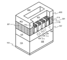
- a pre-metal dielectric (PMD) replacement process is performed by first forming a RMG structure 101 .
- the RMG structure 101 in this example includes a nitride layer 103 ; a silicon layer 105 ; a nitride layer (not shown for illustrative convenience), e.g., an etch stop layer; a STI oxide layer 107 ; a plurality of gates 109 ; a contact etch stop layer (CESL) 111 , e.g., formed of a nitride, and a TEOS layer 113 .
- the gates 109 also include a gate cap layer 115 and spacers (not shown for illustrative convenience).
- the TEOS layer 113 is stripped, for example, using a wet dilute hydrofluoric acid (dHF) or SiCoNiTM, selective to nitride, e.g., the CESL 111 and gate cap layer 115 , as depicted in FIG. 2 .
- dHF wet dilute hydrofluoric acid
- SiCoNiTM SiCoNiTM
- the small “bumps” on the left side of the drawing are the tops of fins covered by the CESL 111 .
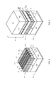
- a SOG layer 301 e.g. formed of a polysilazane-based SOG material, is formed around the RMG structure 101 .
- the SOG layer 301 may be formed, for example, to a thickness of 10 nm to 40 nm using a photo resist coating track through spin and baking at 150° C.
- a TEOS layer 401 is then formed over the SOG layer 301 , as depicted in FIG. 4 . Thereafter, the TEOS layer 401 and the SOG layer 301 are planarized, e.g., by chemical mechanical polishing (CMP), down to gate cap layer 115 , as depicted in FIG. 5 .
- CMP chemical mechanical polishing
- a lithography stack 601 is formed over the SOG layer 301 and the gate cap layer 115 .
- the lithography stack 601 may be formed, for example, of a SOH layer 603 , a SiON layer 605 , a TEOS memory layer 607 , a BARC layer 609 , and a photoresist layer 611 .
- the lithography stack 601 is then double-patterned, for example, using two different color TS masks in a lithography/etch/lithography/etch (LELE) scheme.
- a first TS opening is patterned, for example, through the photoresist layer 611 down to the BARC layer 609 , as depicted in FIG. 7 .
- the first TS opening is etched through the BARC layer 609 and the TEOS memory layer 607 down to the SiON layer 605 , and then the photoresist layer 611 and the BARC layer 609 are removed.
- a BARC layer 901 is formed over the TEOS memory layer 607 and in the first TS opening, as depicted in FIG. 9 .
- a photoresist layer 903 is then formed over the BARC layer 901 .
- the second TS opening is patterned (not shown for illustrative convenience), for example, through the photoresist layer 903 down to the BARC layer 901 .
- the second TS opening is etched through the BARC layer 901 and the TEOS memory layer 607 down to the SiON layer 605 , and then the photoresist layer 903 and the BARC layer 901 are removed, as depicted in FIG. 10 .
- the SiON layer 605 is etched, e.g., by punch etching, non-selective to the TEOS memory layer 607 and, therefore, removing the TEOS memory layer 607 , as depicted in FIG. 11 .
- the SOH layer 603 is etched through the first and second TS openings in the SiON layer 605 down to the SOG layer 301 .
- a portion of the SOG layer 301 is then removed through the first and second TS openings by RIE, as depicted in FIG. 13 .
- the SOG layer 301 is soft relative to SiO 2 , it is easy to etch selective to nitride, e.g., the CESL 111 and the gate cap layer 115 .
- nitride e.g., the CESL 111 and the gate cap layer 115 .
- polysilazane contains S—H, S—N bonds and, therefore, may be etched, for example, with chlorine (Cl) and fluorine (F) containing plasma, hexafluorobutadiene (C 4 F 6 ) with oxygen (O 2 ), or octafluorocyclobutane (C 4 F 8 ) with O 2 . Consequently, no gouging of the Rx area is expected.
- the SiON layer 605 is etched selective (imperfect selectivity) to the SOG layer 301 , the CESL 111 , and the gate cap layer 115 .
- the SOH layer 603 is stripped, and the SOG layer 301 is converted to a SiO 2 layer 1501 , as depicted in FIG. 15 .
- the SOG layer 301 is converted to the SiO 2 layer 1501 , for example, by heating the SOG layer 301 in a high temperature furnace at a temperature of 600° C. to 800° C. for approximately one hour or heating the SOG layer 301 at a temperature of 600° C. in a wet anneal condition for 30 minutes.
- the CESL 111 is etched in the first and second TS openings, as depicted in FIG. 16 .
- the etching of the CESL 111 will also erode some of the gate cap layer 115 .
- a barrier layer (not shown for illustrative convenience) is then formed, e.g., of Ti or TiN, over the SiO 2 layer 1501 and the gate cap layer 115 and in the first and second TS openings.
- a metal layer 1701 is formed, for example, of W, over the barrier layer.
- the metal layer 1701 and the SiO 2 layer 1501 are then planarized, e.g., by CMP, down to the gate cap layer 115 , as depicted in FIG. 18 .
- the embodiments of the present disclosure can achieve several technical effects including taking advantage of siloxane and organic-based materials to enable direct patterning of the S/D contacts of a RMG device without gouging the Rx area or replacing materials.
- Embodiments of the present disclosure enjoy utility in various industrial applications as, for example, microprocessors, smart phones, mobile phones, cellular handsets, set-top boxes, DVD recorders and players, automotive navigation, printers and peripherals, networking and telecom equipment, gaming systems, and digital cameras.
- the present disclosure therefore has industrial applicability in the 10 nm technology node and beyond.
Landscapes
- Engineering & Computer Science (AREA)
- Manufacturing & Machinery (AREA)
- Internal Circuitry In Semiconductor Integrated Circuit Devices (AREA)
Abstract
Description
Claims (19)
Priority Applications (1)
| Application Number | Priority Date | Filing Date | Title |
|---|---|---|---|
| US14/993,537 US10056458B2 (en) | 2016-01-12 | 2016-01-12 | Siloxane and organic-based MOL contact patterning |
Applications Claiming Priority (1)
| Application Number | Priority Date | Filing Date | Title |
|---|---|---|---|
| US14/993,537 US10056458B2 (en) | 2016-01-12 | 2016-01-12 | Siloxane and organic-based MOL contact patterning |
Publications (2)
| Publication Number | Publication Date |
|---|---|
| US20170200792A1 US20170200792A1 (en) | 2017-07-13 |
| US10056458B2 true US10056458B2 (en) | 2018-08-21 |
Family
ID=59276434
Family Applications (1)
| Application Number | Title | Priority Date | Filing Date |
|---|---|---|---|
| US14/993,537 Active 2036-03-31 US10056458B2 (en) | 2016-01-12 | 2016-01-12 | Siloxane and organic-based MOL contact patterning |
Country Status (1)
| Country | Link |
|---|---|
| US (1) | US10056458B2 (en) |
Citations (10)
| Publication number | Priority date | Publication date | Assignee | Title |
|---|---|---|---|---|
| US5459086A (en) * | 1994-11-07 | 1995-10-17 | United Microelectronics Corporation | Metal via sidewall tilt angle implant for SOG |
| US5643407A (en) * | 1994-09-30 | 1997-07-01 | Taiwan Semiconductor Manufacturing Company, Ltd. | Solving the poison via problem by adding N2 plasma treatment after via etching |
| US6074939A (en) * | 1997-02-27 | 2000-06-13 | Nec Corporation | Method for fabricating semiconductor device |
| US6165905A (en) * | 1999-01-20 | 2000-12-26 | Philips Electronics, North America Corp. | Methods for making reliable via structures having hydrophobic inner wall surfaces |
| US6645879B2 (en) * | 2001-08-18 | 2003-11-11 | Samsung Electronics Co., Ltd. | Method of forming a silicon oxide layer of a semiconductor device and method of forming a wiring having the same |
| US7482267B2 (en) * | 2005-04-22 | 2009-01-27 | Ami Semiconductor Belgium Bvba | Ion implantation of spin on glass materials |
| US7585786B2 (en) * | 2003-12-10 | 2009-09-08 | Samsung Electronics Co., Ltd. | Methods of forming spin-on-glass insulating layers in semiconductor devices and associated semiconductor device |
| US20130248999A1 (en) * | 1999-09-28 | 2013-09-26 | Glenn A. Glass | Contact resistance reduction employing germanium overlayer pre-contact metalization |
| US20130309856A1 (en) * | 2012-05-15 | 2013-11-21 | International Business Machines Corporation | Etch resistant barrier for replacement gate integration |
| US20160172356A1 (en) * | 2014-12-10 | 2016-06-16 | International Business Machines Corporation | Inter-level dielectric layer in replacement metal gates and resistor fabrication |
-
2016
- 2016-01-12 US US14/993,537 patent/US10056458B2/en active Active
Patent Citations (10)
| Publication number | Priority date | Publication date | Assignee | Title |
|---|---|---|---|---|
| US5643407A (en) * | 1994-09-30 | 1997-07-01 | Taiwan Semiconductor Manufacturing Company, Ltd. | Solving the poison via problem by adding N2 plasma treatment after via etching |
| US5459086A (en) * | 1994-11-07 | 1995-10-17 | United Microelectronics Corporation | Metal via sidewall tilt angle implant for SOG |
| US6074939A (en) * | 1997-02-27 | 2000-06-13 | Nec Corporation | Method for fabricating semiconductor device |
| US6165905A (en) * | 1999-01-20 | 2000-12-26 | Philips Electronics, North America Corp. | Methods for making reliable via structures having hydrophobic inner wall surfaces |
| US20130248999A1 (en) * | 1999-09-28 | 2013-09-26 | Glenn A. Glass | Contact resistance reduction employing germanium overlayer pre-contact metalization |
| US6645879B2 (en) * | 2001-08-18 | 2003-11-11 | Samsung Electronics Co., Ltd. | Method of forming a silicon oxide layer of a semiconductor device and method of forming a wiring having the same |
| US7585786B2 (en) * | 2003-12-10 | 2009-09-08 | Samsung Electronics Co., Ltd. | Methods of forming spin-on-glass insulating layers in semiconductor devices and associated semiconductor device |
| US7482267B2 (en) * | 2005-04-22 | 2009-01-27 | Ami Semiconductor Belgium Bvba | Ion implantation of spin on glass materials |
| US20130309856A1 (en) * | 2012-05-15 | 2013-11-21 | International Business Machines Corporation | Etch resistant barrier for replacement gate integration |
| US20160172356A1 (en) * | 2014-12-10 | 2016-06-16 | International Business Machines Corporation | Inter-level dielectric layer in replacement metal gates and resistor fabrication |
Non-Patent Citations (1)
| Title |
|---|
| Honeywell, "Honeywell Electronic Materials: Electronic Polymers Overview", Dec. 2014, 18 Pages. |
Also Published As
| Publication number | Publication date |
|---|---|
| US20170200792A1 (en) | 2017-07-13 |
Similar Documents
| Publication | Publication Date | Title |
|---|---|---|
| US9960077B1 (en) | Ultra-scale gate cut pillar with overlay immunity and method for producing the same | |
| US9478462B1 (en) | SAV using selective SAQP/SADP | |
| US11217678B2 (en) | Differential SG/EG spacer integration with equivalent NFET/PFET spacer widths and dual raised source drain expitaxial silicon and triple-nitride spacer integration enabling high-voltage EG device on FDSOI | |
| US8518775B2 (en) | Integration of eNVM, RMG, and HKMG modules | |
| US8679968B2 (en) | Method for forming a self-aligned contact opening by a lateral etch | |
| US9419101B1 (en) | Multi-layer spacer used in finFET | |
| TWI527236B (en) | Semiconductor device and method of manufacturing same | |
| US9425097B1 (en) | Cut first alternative for 2D self-aligned via | |
| US10211103B1 (en) | Advanced structure for self-aligned contact and method for producing the same | |
| US9859125B2 (en) | Block patterning method enabling merged space in SRAM with heterogeneous mandrel | |
| CN102543696A (en) | A method of manufacturing a semiconductor device | |
| CN103545185B (en) | A kind of method that use dummy grid manufactures semiconductor devices | |
| CN108878292B (en) | FINFET device and method of forming the same | |
| US20080268589A1 (en) | Shallow trench divot control post | |
| CN106898575B (en) | Semiconductor device, manufacturing method thereof and electronic device | |
| US10056458B2 (en) | Siloxane and organic-based MOL contact patterning | |
| US20140353728A1 (en) | Method and apparatus for a reduced capacitance middle-of-the-line (mol) nitride stack | |
| CN103794479B (en) | A kind of manufacture method of semiconductor device | |
| CN108735670A (en) | A kind of semiconductor devices and its manufacturing method and electronic device | |
| US9972621B1 (en) | Fin structure in sublitho dimension for high performance CMOS application | |
| US9698018B1 (en) | Introducing self-aligned dopants in semiconductor fins | |
| US9875936B1 (en) | Spacer defined fin growth and differential fin width | |
| CN105990237A (en) | Semiconductor device, manufacturing method thereof, and electronic device | |
| CN106910706B (en) | Method for manufacturing semiconductor device | |
| CN103579110B (en) | A kind of manufacture method of semiconductor device |
Legal Events
| Date | Code | Title | Description |
|---|---|---|---|
| AS | Assignment |
Owner name: GLOBALFOUNDRIES INC., CAYMAN ISLANDS Free format text: ASSIGNMENT OF ASSIGNORS INTEREST;ASSIGNORS:MAENG, CHANG HO;WEI, ANDY;OZZELLO, ANTHONY;AND OTHERS;SIGNING DATES FROM 20151215 TO 20151221;REEL/FRAME:037467/0427 |
|
| STCF | Information on status: patent grant |
Free format text: PATENTED CASE |
|
| AS | Assignment |
Owner name: WILMINGTON TRUST, NATIONAL ASSOCIATION, DELAWARE Free format text: SECURITY AGREEMENT;ASSIGNOR:GLOBALFOUNDRIES INC.;REEL/FRAME:049490/0001 Effective date: 20181127 |
|
| AS | Assignment |
Owner name: GLOBALFOUNDRIES U.S. INC., CALIFORNIA Free format text: ASSIGNMENT OF ASSIGNORS INTEREST;ASSIGNOR:GLOBALFOUNDRIES INC.;REEL/FRAME:054633/0001 Effective date: 20201022 |
|
| AS | Assignment |
Owner name: GLOBALFOUNDRIES INC., CAYMAN ISLANDS Free format text: RELEASE BY SECURED PARTY;ASSIGNOR:WILMINGTON TRUST, NATIONAL ASSOCIATION;REEL/FRAME:054636/0001 Effective date: 20201117 |
|
| AS | Assignment |
Owner name: GLOBALFOUNDRIES U.S. INC., NEW YORK Free format text: RELEASE BY SECURED PARTY;ASSIGNOR:WILMINGTON TRUST, NATIONAL ASSOCIATION;REEL/FRAME:056987/0001 Effective date: 20201117 Owner name: GLOBALFOUNDRIES U.S. INC., NEW YORK Free format text: RELEASE OF SECURITY INTEREST;ASSIGNOR:WILMINGTON TRUST, NATIONAL ASSOCIATION;REEL/FRAME:056987/0001 Effective date: 20201117 |
|
| MAFP | Maintenance fee payment |
Free format text: PAYMENT OF MAINTENANCE FEE, 4TH YEAR, LARGE ENTITY (ORIGINAL EVENT CODE: M1551); ENTITY STATUS OF PATENT OWNER: LARGE ENTITY Year of fee payment: 4 |
|
| FEPP | Fee payment procedure |
Free format text: MAINTENANCE FEE REMINDER MAILED (ORIGINAL EVENT CODE: REM.); ENTITY STATUS OF PATENT OWNER: LARGE ENTITY |