US10050466B2 - DC-charging power source adaptor and mobile terminal - Google Patents
DC-charging power source adaptor and mobile terminal Download PDFInfo
- Publication number
- US10050466B2 US10050466B2 US15/051,851 US201615051851A US10050466B2 US 10050466 B2 US10050466 B2 US 10050466B2 US 201615051851 A US201615051851 A US 201615051851A US 10050466 B2 US10050466 B2 US 10050466B2
- Authority
- US
- United States
- Prior art keywords
- charging
- power source
- voltage
- mobile terminal
- controller
- Prior art date
- Legal status (The legal status is an assumption and is not a legal conclusion. Google has not performed a legal analysis and makes no representation as to the accuracy of the status listed.)
- Active, expires
Links
- 238000007600 charging Methods 0.000 title claims abstract description 552
- 230000008859 change Effects 0.000 claims abstract description 20
- 238000004891 communication Methods 0.000 claims description 120
- 230000001360 synchronised effect Effects 0.000 claims description 29
- 230000005540 biological transmission Effects 0.000 claims description 16
- 238000013459 approach Methods 0.000 claims description 12
- 230000004044 response Effects 0.000 claims description 11
- 230000009466 transformation Effects 0.000 claims description 7
- 238000005070 sampling Methods 0.000 claims description 6
- 230000003287 optical effect Effects 0.000 claims description 4
- 230000003111 delayed effect Effects 0.000 claims 2
- 238000000034 method Methods 0.000 description 20
- 230000008569 process Effects 0.000 description 16
- 230000002159 abnormal effect Effects 0.000 description 12
- 230000006870 function Effects 0.000 description 7
- 230000007246 mechanism Effects 0.000 description 6
- 238000001514 detection method Methods 0.000 description 5
- 230000037361 pathway Effects 0.000 description 5
- 238000010586 diagram Methods 0.000 description 4
- 238000010277 constant-current charging Methods 0.000 description 3
- 230000001419 dependent effect Effects 0.000 description 3
- 230000005856 abnormality Effects 0.000 description 2
- 230000008901 benefit Effects 0.000 description 2
- 238000011217 control strategy Methods 0.000 description 2
- 230000003247 decreasing effect Effects 0.000 description 2
- 238000011161 development Methods 0.000 description 2
- 230000018109 developmental process Effects 0.000 description 2
- 238000012986 modification Methods 0.000 description 2
- 230000004048 modification Effects 0.000 description 2
- 230000000630 rising effect Effects 0.000 description 2
- 238000012935 Averaging Methods 0.000 description 1
- 102100035954 Choline transporter-like protein 2 Human genes 0.000 description 1
- 101000948115 Homo sapiens Choline transporter-like protein 2 Proteins 0.000 description 1
- 230000032683 aging Effects 0.000 description 1
- 230000009286 beneficial effect Effects 0.000 description 1
- 238000006243 chemical reaction Methods 0.000 description 1
- 238000010280 constant potential charging Methods 0.000 description 1
- 238000003745 diagnosis Methods 0.000 description 1
- 201000010099 disease Diseases 0.000 description 1
- 208000037265 diseases, disorders, signs and symptoms Diseases 0.000 description 1
- 238000005516 engineering process Methods 0.000 description 1
- 230000003071 parasitic effect Effects 0.000 description 1
- 239000004065 semiconductor Substances 0.000 description 1
- 229910052710 silicon Inorganic materials 0.000 description 1
- 239000010703 silicon Substances 0.000 description 1
- 230000009897 systematic effect Effects 0.000 description 1
Images


Classifications
-
- H—ELECTRICITY
- H02—GENERATION; CONVERSION OR DISTRIBUTION OF ELECTRIC POWER
- H02J—CIRCUIT ARRANGEMENTS OR SYSTEMS FOR SUPPLYING OR DISTRIBUTING ELECTRIC POWER; SYSTEMS FOR STORING ELECTRIC ENERGY
- H02J7/00—Circuit arrangements for charging or depolarising batteries or for supplying loads from batteries
- H02J7/02—Circuit arrangements for charging or depolarising batteries or for supplying loads from batteries for charging batteries from ac mains by converters
-
- H02J7/045—
-
- H—ELECTRICITY
- H02—GENERATION; CONVERSION OR DISTRIBUTION OF ELECTRIC POWER
- H02J—CIRCUIT ARRANGEMENTS OR SYSTEMS FOR SUPPLYING OR DISTRIBUTING ELECTRIC POWER; SYSTEMS FOR STORING ELECTRIC ENERGY
- H02J7/00—Circuit arrangements for charging or depolarising batteries or for supplying loads from batteries
- H02J7/007—Regulation of charging or discharging current or voltage
- H02J7/00712—Regulation of charging or discharging current or voltage the cycle being controlled or terminated in response to electric parameters
- H02J7/00714—Regulation of charging or discharging current or voltage the cycle being controlled or terminated in response to electric parameters in response to battery charging or discharging current
-
- H—ELECTRICITY
- H02—GENERATION; CONVERSION OR DISTRIBUTION OF ELECTRIC POWER
- H02J—CIRCUIT ARRANGEMENTS OR SYSTEMS FOR SUPPLYING OR DISTRIBUTING ELECTRIC POWER; SYSTEMS FOR STORING ELECTRIC ENERGY
- H02J7/00—Circuit arrangements for charging or depolarising batteries or for supplying loads from batteries
- H02J7/007—Regulation of charging or discharging current or voltage
- H02J7/00712—Regulation of charging or discharging current or voltage the cycle being controlled or terminated in response to electric parameters
- H02J7/007182—Regulation of charging or discharging current or voltage the cycle being controlled or terminated in response to electric parameters in response to battery voltage
-
- H02J7/022—
-
- H02J2007/0062—
-
- H02J2007/0096—
-
- H—ELECTRICITY
- H02—GENERATION; CONVERSION OR DISTRIBUTION OF ELECTRIC POWER
- H02J—CIRCUIT ARRANGEMENTS OR SYSTEMS FOR SUPPLYING OR DISTRIBUTING ELECTRIC POWER; SYSTEMS FOR STORING ELECTRIC ENERGY
- H02J2207/00—Indexing scheme relating to details of circuit arrangements for charging or depolarising batteries or for supplying loads from batteries
- H02J2207/20—Charging or discharging characterised by the power electronics converter
-
- H—ELECTRICITY
- H02—GENERATION; CONVERSION OR DISTRIBUTION OF ELECTRIC POWER
- H02J—CIRCUIT ARRANGEMENTS OR SYSTEMS FOR SUPPLYING OR DISTRIBUTING ELECTRIC POWER; SYSTEMS FOR STORING ELECTRIC ENERGY
- H02J7/00—Circuit arrangements for charging or depolarising batteries or for supplying loads from batteries
- H02J7/00032—Circuit arrangements for charging or depolarising batteries or for supplying loads from batteries characterised by data exchange
- H02J7/00034—Charger exchanging data with an electronic device, i.e. telephone, whose internal battery is under charge
Definitions
- the present disclosure relates to the field of Direct-Current (DC) charging and particularly to a power source adaptor for charging rapidly a battery in a mobile terminal.
- DC Direct-Current
- portable electronic products have been widely applied in numerous aspects of people's life, and have become a leading factor in the development of the semiconductor industry.
- portable electronic products e.g., MP3, MP4, PMP, MID, mobile TV terminals, tablet computers, etc.
- these portable electronic products can provide audio and video playing, and other entertainment functions, and also provide navigation, an access to the Internet, business, disease diagnosis, and other service functions to thereby greatly facilitate people's life.
- the portable electronic products are generally provided with chargeable batteries built in the products to power system circuits in the products.
- the batteries have been widely charged in two general schemes: in one of the schemes, the batteries are charged by a specialized power source adaptor (charger), i.e., in the standard DCP charging scheme, where the power source adaptor generally supports an output of only fixed voltage, e.g., 5V, 9V, 12V, etc., so that the output voltage may not be selectable flexibly, and it may take a long period of time to charge the batteries, for example, it typically takes 3 to 4 hours to charge a drained battery of a handset until the battery is fully charged; and in the other scheme, the batteries are charged by a host (e.g., a computer, etc.), i.e., in the SDP charging scheme.
- a host e.g., a computer, etc.
- This disclosure provides a DC-charging power source adaptor including a charging interface, an AC to DC converting unit, and a controlling unit, wherein the charging interface is configured to be connected with a mobile terminal, and including a power source pin, a ground pin, and two communication pins shorted by default; the AC to DC converting unit is configured to convert an external AC input power source into charging voltage required for the mobile terminal, and to output the charging voltage via the charging interface; and the controlling unit, connected with the charging interface, is configured to control the two communication pins of the charging interfaces to be disconnected from each other upon detecting that the charging interface is connected with the mobile terminal, and to communicate with the mobile terminal through the two communication pins to adjust the charging voltage output by the AC to DC converting unit.
- This disclosure further provides a mobile terminal including: a communicating and receiving interface configured to communicate with a DC-charging power source adaptor to send a change in voltage of a battery in the mobile terminal to the DC-charging power source adaptor so that the DC-charging power source adaptor adjusts dynamically a volt value of charging voltage output by the DC-charging power source adaptor according to the change in voltage, and to receive the charging voltage input by the DC-charging power source adaptor; and a sending unit to send a specific pulse waveform to the DC-charging power source adaptor after the mobile terminal is connected with the DC-charging power source adaptor.
- FIG. 1 is a circuit scheme block diagram of an embodiment of a mobile terminal and a DC-charging power source adaptor, both of which are connected, according to this disclosure;
- FIG. 2 is a circuit scheme diagram of an embodiment of the DC-charging power source adaptor in FIG. 1 ;
- FIG. 3 is a flow chart of a process of a charging method designed for the mobile terminal illustrated in FIG. 1 ;
- FIG. 4 is a flow chart of an embodiment of detecting communication between the mobile terminal and the DC-charging power source adaptor illustrated in FIG. 1 ;
- FIG. 5 is a flow chart of an embodiment of a timed detection mechanism of communication between the mobile terminal and the DC-charging power source adaptor illustrated in FIG. 1 ;
- FIG. 6 is a flow chart of control in an embodiment of a DC-charging control strategy using a lookup table
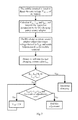
- FIG. 7 is a flow chart of control in an embodiment of a voltage-following DC-charging control strategy.
- FIG. 8 is a schematic diagram of a mobile terminal according to this disclosure.
- This disclosure proposes a DC-charging power source adaptor outputting dynamically adjustable voltage to address such a problem that if a mobile terminal in which a chargeable battery is built is charged, then charging voltage output by a normal power source adaptor is constant, and charging current has to be controlled by a power source managing chip not to be too high, typically below 1.5 A, so it may take a long period of time to charge the drained battery until the battery is fully charged.
- the DC-charging power source adaptor can exchange data with the mobile terminal to be charged in the UART (Universal Asynchronous Receiver/Transmitter) communication mode, adjust duly a voltage value of the charging voltage output by the DC-charging power source adaptor according to a change in voltage of the battery being charged, and DC-charge the battery in the mobile terminal using the dynamically changing charging voltage, so that the battery in the mobile terminal can be charged at higher voltage to thereby maintain the charging current at a higher current value, typically up to approximately 4 A, and the battery can be charged directly at the larger current to thereby significantly speed up charging and greatly shorten the period of time for charging.
- UART Universal Asynchronous Receiver/Transmitter
- the existing charging interface of the mobile terminal is maintained in this embodiment, e.g., the currently widely applied USB interface Ji (for both charging and transmitting data), so that the mobile terminal can be plugged in and powered by the normal power source adaptor and computer host in the market, which are currently manufactured by the majority of the manufactures.
- the power source pin VBUS in the USB interface Ji in this embodiment, one branch thereof is connected with a power source managing chip in the mobile terminal, and another branch thereof is connected with the battery through a DC-charging switch, where the DC-charging switch can be any type of controllable switch element with low conduction impedance and supporting large current to pass, e.g., controllable silicon, an MOS transistor, etc., to receive a switch control signal output by a microprocessor in the mobile terminal to selectively switch between the normal charging mode and the rapid charging mode.
- the ground pin GND in the USB interface Ji it can be well connected with a systematical ground of the mobile terminal so that the mobile terminal can be grounded together with the external charging device if the mobile terminal is plugged in the external device.
- the differential data pins D+ and D ⁇ in the USB interface Ji are designed to be connected with the microprocessor through a gating switch, where the gating switch can be a double-pole double-throw switch, to receive a control signal output by the microprocessor, where the differential data pins D+ and D ⁇ of the USB interface Ji are connected by default with the differential data interfaces DP and DN of the microprocessor through the gating switch; and if it is detected that the differential data pins D+ and D ⁇ of the USB interface Ji are shorted, then the gating switch will be controlled by the microprocessor to switch the differential data pins D+ and D ⁇ of the USB interface Ji to be connected with the UART interfaces TXD and RXD of the microprocessor to thereby identify whether the externally connected charging device is the normal power source adaptor or the DC-charging power source adaptor.
- the gating switch can be a double-pole double-throw switch, to receive a control signal output by the microprocessor, where the differential data pin
- the microprocessor in the mobile terminal can be designed to conduct UART communication with the externally connected power source adaptor after the differential data pins D+ and D ⁇ of the USB interface Ji are switched to be connected with the UART interfaces TXD and RXD of the microprocessor, and if the communication succeeds, to determine that the inserted external device is the DC-charging power source adaptor; otherwise, to determine that the inserted external device is the normal power source adaptor.
- the DC-charging power source adaptor is configured in the UART communication mode instead of the I2C bus communication mode for the reason that there is small communication traffic, a low rate, and a high anti-interference capability of UART communication in the asynchronous communication mode to thereby avoid effectively communication between the mobile terminal and the power source adaptor from becoming highly instable due to interference from current, impedance, voltage, and other signals so that the mobile terminal can be charged stably and rapidly at large current by the DC-charging power source adaptor to thereby improve the safety of the mobile terminal being charged.
- communication between the mobile terminal and the DC-charging power source adaptor can be designed in another communication mode than UART (e.g., the I2C bus communication mode, etc.) although this embodiment will not be limited thereto.
- UART e.g., the I2C bus communication mode, etc.
- FIG. 2 illustrates a schematic diagram of circuit components of a DC-charging power source adaptor supporting UART communication
- the DC-charging power source adaptor generally includes three components, i.e., a charging interface Jo, a controlling unit, and an AC-DC (converting) unit, as illustrated in FIG. 1 as well, where a power source pin Vbus, a ground pin Gnd, and two communication pins Tx and Rx are arranged in the charging interface Jo.
- the power source pin Vbus configured to transmit a charging power source is connected with the AC-DC unit to transmit a DC power source output by the AC-DC unit to the power source pin VBUS of the USB interface Ji of the mobile terminal to charge the mobile terminal.
- the ground pin Gnd is connected with the system ground of the DC-charging power source adaptor, and after the DC-charging power source adaptor is plugged in the mobile terminal, the ground pin Gnd is connected with the ground pin GND of the USB interface Ji of the mobile terminal so that both of the ground pins are grounded together.
- the two communication pins Tx and Rx of the charging interface Jo are shorted by default, and connected with the respective UART interfaces TX and RX of the controlling unit.
- the controlling unit may control the two communication pins Tx and Rx of the charging interface Jo to be switched from being shorted by default to be disconnected from each other, and then send a communication command on its own initiative to the mobile terminal through the UART interfaces TX and RX thereof, conduct UART communication with the mobile terminal to exchange a handshake instruction with each other, receive control information sent by the mobile terminal if the handshake succeeds, and further adjust the volt value of the charging voltage output by the AC-DC unit according to the control information so that the mobile terminal can be charged differently as required in different phases.
- the mobile terminal can alternatively be configured to be timed to send a UART communication command to the externally connected power source adaptor, and to wait for a response command fed back by the DC-charging power source adaptor, in a preset wait period of time after the differential data pins D+ and D ⁇ of the USB interface Ji are switched to be connected with the UART interfaces TXD and RXD of the microprocessor of the mobile terminal, and if a valid response command is received in the wait period of time, to determine that the external device is the DC-charging power source adaptor; otherwise, to determine that the external device is the normal power source adaptor.
- the wait period of time shall be longer than the preset period of time so that the DC-charging power source adaptor can receive and respond to the UART communication command sent by the mobile terminal, after the communication pins Tx and Rx of the DC-charging power source adaptor are disconnected from each other.
- controlling unit can alternatively be designed to further control the two communication pins Tx and Rx of the charging interface Jo to be switched to be connected with or disconnected from each other, upon reception of a specific pulse waveform sent by the mobile terminal.
- the controlling unit can be configured to firstly configure by default the UART interfaces TX and RX thereof to receive an input, and if the mobile terminal detects that the externally inserted device is a power source adaptor, and the microprocessor of the mobile terminal switches the UART interfaces TXD and RXD thereof to be connected with the differential data pins D+ and D ⁇ of the USB interface Ji, then firstly the specific pulse waveform will be output by the microprocessor to the externally connected power source adaptor.
- the controlling unit in the DC-charging power source adaptor will receive the specific pulse waveform even if the communication pins Tx and Rx are shorted because the UART interfaces TX and RX of the controlling unit are configured to receive an input.
- the controlling unit switches the communication pins Tx and Rx of the charging interface Jo from being shorted by default to be disconnected from each other, and recover the communication interface function of the UART interfaces TX and RX of the controlling unit, upon reception of the specific pulse waveform.
- the microprocessor in the mobile terminal can be configured to send constantly the specific pulse waveform for a preset period of time which can be determined as a function of a period of time from when the DC-charging power source adaptor receives the specific pulse waveform to when the DC-charging power source adaptor controls the communication pins Tx and Rx thereof to be connected with or disconnected from each other.
- the microprocessor initiates a communication command on its own initiative to the externally connected power source adaptor in the UART communication mode, and if a valid command fed back by the external power source adaptor is received, then the microprocessor determines that the external device is the DC-charging power source adaptor, and starts the rapid charging mode; and if there is no valid command fed back, then the microprocessor determines that the external device is the normal power source adaptor, and at this time the microprocessor disconnects the UART interfaces TXD and RXD thereof from the differential data pins D+ and D ⁇ of the USB interface Ji, and starts the standard DCP charging mode.
- a rectifying circuit, a transformer unit, a synchronous rectification controller, a PWM controller, an optical coupler, a power MOS transistor, and other elements are designed in the AC-DC unit; and a controller, a digital potentiometer, a current detecting chip, a boosting circuit, and other elements are designed in the controlling unit, as illustrated in FIG. 2 , where the rectifying circuit receives an AC input power source AC_IN provided by a mains grid, rectifies the AC input power source into a DC power source, and outputs the DC power source to the transformer unit for transformation into the charging voltage to charge the mobile terminal.
- the UART interfaces TX 2 and RX 2 of the controller are connected with the communication pins Tx and Rx of the charging interface Jo through two signal lines across which a switch K is connected, where the switch is closed by default to short the communication pins Tx and Rx. If the controller receives the specific pulse waveform, or if the controller detects that the DC-charging power source adaptor is plugged in the mobile terminal and after delaying a preset period of time (dependent upon the configuration of the controller), then the controller will output a control signal to the switch K through an interface CTL 2 (e.g., a branch of GPIO interface) of the controller to control the switch K to be opened, and further create a UART communication line between the DC-charging power source adaptor and the mobile terminal.
- an interface CTL 2 e.g., a branch of GPIO interface
- the magnitude of the charging current output through the power source pin Vbus of the charging interface Jo can be detected to thereby determine whether the DC-charging power source adaptor is connected with the mobile terminal. If the DC-charging power source adaptor is not connected with the mobile terminal, then the charging current output through the power source pin Vbus may be substantially zero. If the DC-charging power source adaptor is connected with the mobile terminal, then there may be some charging current even if the battery of the mobile terminal is fully charged. Thus the DC-charging power source adaptor can determine from the magnitude of the charging current whether it is connected with the external mobile terminal.
- the digital potentiometer is designed in the controlling unit to be connected with the controller.
- the controller generates a voltage adjusting instruction according to the received control information, and sends the voltage adjusting instruction to the digital potentiometer to change the resistance value of a valid resistor of the digital potentiometer.
- the controller can be connected and communicates with the digital potentiometer over an I2C bus, as illustrated in FIG. 2 , to transmit the voltage adjusting instruction.
- a voltage pull-up circuit is further connected over the I2C bus, for example, a clock line SCL and a data line SDA of the I2C bus are connected with a DC power source VDD respectively through pull-up resistors R 2 and R 3 to thereby improve the anti-interference capability of the transmission of the signal.
- the DC power source VDD can be embodied as a set of small electromagnetic coils designed separately in the transformer unit.
- the ratio of the number of turns of a primary coil and the number of turns of a secondary coil in the set of small electromagnetic coils is configured to transform the DC power source output by the rectifying circuit into the desirable DC power source VDD to power those components in the DC-charging power source adaptor to provide the components with desirable DC operating voltage, e.g., the controller, the digital potentiometer, the current detecting chip, and other components to thereby enable them to operate.
- the digital potentiometer is a resistance-adjustable resistor element in which a resistor body is built.
- the resistor body connected in series with a current-limiting resistor R 1 is connected between the anode of a secondary coil in another set of electromagnetic coils (referred below simply to as the other set of electromagnetic coils) in the transformer unit and the ground.
- One end P 0 A of the resistor body is connected with the anode of the secondary coil in the other set of electromagnetic coils through the current-limiting resistor R 1 connected in series, and the other end P 0 B of the resistor body is grounded.
- An intermediate tap POW of the resistor body is connected with a reference voltage pin VREF of the synchronous rectification controller, and if the resistance value of the valid resistor of the digital potentiometer varies, then the volt value of the charging voltage output by the other set of electromagnetic coils in the transformer unit will be adjusted in order to maintain the reference voltage on the reference voltage pin VREF of the synchronous rectification controller.
- the synchronous rectification controller adjusts its output control signal according to the varying resistance value of the valid resistor of the digital potentiometer, and transmits the control signal to the PWM controller after the control signal is optic-electrically isolated by the optical coupler, to thereby adjust a duty ratio of a PWM signal output by the PWM controller.
- the PWM signal is transmitted to the transformer unit, and can be transmitted to a switch transistor connected in series with a primary coil in the other set of electromagnetic coils, to control the switch transistor to be switched on or off to thereby adjust the switching timing of the other set of electromagnetic coils so as to further adjust the volt value of the charging voltage output by the secondary coil thereof for the purpose of adjusting dynamically the charging voltage.
- the charging voltage output by the transformer unit can be finely adjusted in the range of 3.6V to 12V to thereby charge different mobile terminals as required in reality.
- the power MOS transistor is connected on the charging voltage transmission line and is switched on or off based on the switching signal output by the synchronous rectification controller to thereby shape the waveform of the charging voltage output by the transformer unit.
- the power MOS transistor can be embodied as an NMOS transistor connected between the cathode of the secondary coil in the other set of electromagnetic coils and the ground pin Gnd of the charging interface Jo. Since the DC-charging power source adaptor supports an output of large current, if the charging voltage output by the transformer unit is shaped by the diode, then power consumption of the DC-charging power source adaptor may be increased and the efficiency in charging may be lowered due to a significant voltage drop across the conducting diode. In this embodiment, the charging voltage is shaped by the power MOS transistor, and since the power MOS transistor has low inner resistance and supports large current passing, systematic power consumption of the DC-charging power source adaptor can be lowered effectively and the efficiency in charging the mobile terminal can be improved.
- a sampling resistor R 6 is further connected in series in the transmission line of the charging current, as illustrated in FIG. 2 , possibly between the anode of the secondary coil in the other set of electromagnetic coils in the transformer unit and the power source pin Vbus of the charging interface Jo.
- Inputs ⁇ IN and +IN of the current detecting chip are connected with two ends of the sampling resistor R 6 to acquire a voltage drop across the resistor R 6 , and after the voltage drop is amplified, the magnitude of the charging current is calculated according to the voltage drop and the resistance value of the sampling resistor R 6 .
- the current detecting chip generates sample voltage corresponding to the calculated magnitude of the charging current, and transmits the sample voltage to an ADC interface AD 1 of the controller through an output OUT thereof, and the sample voltage is analog-to-digital converted by the controller into the magnitude of the charging current, so the controller can detect in real time the charging current.
- a voltage dividing circuit can be additionally arranged between the output OUT of the current detecting chip and the ADC interface AD 1 of the controller, e.g., a resistor voltage dividing circuit composed of resistors R 4 and R 5 , to adjust the voltage signal output by the current detecting chip within the interface voltage range acceptable to the AD 1 interface of the controller so as to avoid the ADC interface AD 1 of the controller from being damaged due to the input voltage being too high.
- a switch transistor Q 1 supporting large current passing is further arranged in the charging power source transmission line of the DC-charging power source adaptor so that a switch voltage, generated by the boosting circuit, sufficient to drive the switch transistor Q 1 to be switched on is transmitted to a control pole of the switch transistor Q 1 to control the switch transistor Q 1 to be switched on or off to thereby have the charging power source transmission line connected or disconnected.
- the switch transistor can be embodied as a pair of NMOS transistors Q 1 in which parasitic diodes connected in anti-parallel are built, as illustrated in FIG. 2 .
- the switch path of the pair of NMOS transistors Q 1 are connected in series in the transmission line of the charging power source, where the sources of the two NMOS transistors in the pair of NMOS transistors Q 1 can be connected with each other, the drains of the two NMOS transistors can be connected respectively with the anode of the secondary coil in the other set of electromagnetic coils in the transformer unit, and the power source pin Vbus of the charging interface Jo; and then the gates of the two NMOS transistors can be connected with the boosting circuit.
- An enable end of the boosting circuit is connected with the controller to receive an enable signal output by the controller.
- the controller may output the valid enable signal to control the boosting circuit to be enabled into operation to boost the DC power source output by the transformer unit to the switch voltage higher than the volt value of the charging voltage, and the switch voltage is output to the gates of the pair of NMOS transistors Q 1 to control the pair of NMOS transistors Q 1 to be switched on to have the transmission line of the charging power source connected, so that the charging power source can be output to the externally connected mobile terminal to charge the battery in the mobile terminal.
- the controller may output the invalid enable signal to control the boosting circuit to stop operating.
- the pair of NMOS transistors Q 1 is switched off due to the disappearing voltage at the gates thereof, to thereby have the transmission line of the charging power source disconnected to block the charging power source from outputting to the outside, so that the DC-charging power source adaptor can be controlled to stop powering the mobile terminal.
- this disclosure proposes a charging method as described below for the host and the normal power source adaptor, and the DC-charging power source adaptor according to this embodiment, in addition to the circuitry modifications as illustrated in FIG. 1 for the hardware configuration of the mobile terminal.
- a charging method generally involves the following operations:
- the mobile terminal detects whether an external device is inserted, and performs subsequent operations upon detecting an inserted external device.
- detection of whether an external device is inserted can be performed as in the prior art, for example, by detecting whether a DC power source is connected to the power source pin VBUS of the USB interface Ji of the mobile terminal.
- the charging voltage output by the host and the normal power source adaptor is typically 5V; and the DC-charging power source adaptor can be configured to output by default the same constant charging voltage as the host and the normal power source adaptor, e.g., 5V constant charging voltage so that the mobile terminal can substantially determine whether the DC-charging power source adaptor is inserted.
- the DC-charging power source adaptor will be simply configured to output by default the same constant charging voltage as the charging voltage output by the normal power source adaptor when the normal power source adaptor powers the mobile terminal.
- the mobile terminal detects the type of the inserted external device.
- the mobile terminal operates by default without being DC-charged, that is, the microprocessor in the mobile terminal controls by default the DC-charging switch to be opened to have the power source pin VBUS of the USB interface Ji connected with the power source managing chip. Also the microprocessor controls the gating switch to be kept in the default state to have the differential data pins D+ and D ⁇ of the USB interface Ji connected with the differential data interfaces DP and DN of the microprocessor.
- Whether the inserted external device is the host or the normal power source adaptor can be determined as in the existing BC1.2 charging type detection scheme. Of course this can alternatively be determined as follows:
- the microprocessor firstly determines whether the differential data pins D+ and D ⁇ of the USB interface Ji are shorted, and if the differential data pins D+ and D ⁇ are not shorted, then the mobile terminal determines that the inserted external device is the host because the existing host (e.g., the computer host) typically is connected and communicates with and powers the mobile terminal through the USB data line.
- the mobile terminal can further conduct USB communication with the externally inserted external device via the differential data interfaces DP and DN of the microprocessor to further determine whether the inserted external device is the host.
- the mobile terminal determines that the inserted external device is a power source adaptor because the communication pins of the existing normal power source adaptor typically are configured to be shorted. Moreover in this embodiment, in order to be identified by the mobile terminal in the same way as the normal power source adaptor, the communication pins Tx and Rx of the DC-charging power source adaptor can also be configured to be shorted by default. If the mobile terminal determines that the inserted external device is a power source adaptor, then the mobile terminal can communicate with the externally connected power source adaptor to further determine whether the inserted external device is the normal power source adaptor or the DC-charging power source adaptor.
- the microprocessor If the microprocessor detects that the differential data pins D+ and D ⁇ of the USB interface Ji of the mobile terminal are shorted, then the microprocessor firstly controls the gating switch to operate to switch the differential data pins D+ and D ⁇ of the USB interface Ji to be connected with the UART interfaces TXD and RXD of the microprocessor. Then the microprocessor outputs a specific pulse waveform to the externally connected power source adaptor through the UART interfaces TXD and RXD of the microprocessor in a preset period of time.
- the microprocessor After the preset period of time expires, the microprocessor initiates a communication command on its own initiative to the externally connected power source adaptor in the UART communication mode, and if a valid response command fed back by the externally connected power source adaptor is received, then the microprocessor determines that the inserted external device is the DC-charging power source adaptor (because at this time the DC-charging power source adaptor has the communication pins Tx and Rx of the charging interface Jo thereof switched from being shorted to be connected with the UART interfaces TX 2 and RX 2 of the controller thereof); otherwise, the microprocessor determines that the inserted external device is the normal power source adaptor.
- the microprocessor can alternatively determine this as follows: after the microprocessor controls the UART interfaces TXD and RXD thereof to be connected with the respective differential data pins D+ and D ⁇ of the USB interface Ji, the microprocessor waits for reception of a UART communication command initiated by the DC-charging power source adaptor on its own initiative. If the UART communication command is received in a preset wait period of time, then the mobile terminal determines that the inserted external device is the DC-charging power source adaptor; otherwise, the mobile terminal determines that the inserted external device is the normal power source adaptor.
- the microprocessor is timed to send a UART communication command to the externally connected power source adaptor, and waits for a response command fed back by the external power source adaptor, in a preset wait period of time, and if a valid response command is received, then the mobile terminal determines that the inserted external device is the DC-charging power source adaptor; otherwise, the mobile terminal determines that the inserted external device is the normal power source adaptor.
- the microprocessor determines that the inserted external device is the DC-charging power source adaptor, in order to enable a better switching mechanism and error-tolerant mechanism, in this embodiment, communication between the mobile terminal and the DC-charging power source adaptor can be detected in the following flow as illustrated in FIG. 4 : the microprocessor initiates a communication command A on its own initiative to the external power source adaptor after switching the communication interface of the microprocessor from the differential data interfaces DP and DN to the UART interfaces TXD and RXD, and also counts the number of communications.
- the DC-charging power source adaptor receiving successfully the communication command A can respond accordingly by sending a communication command B to the mobile terminal, and if the mobile terminal does not receive any valid communication command B, then the microprocessor firstly determines the count of communications at that time, and if the count of communications is less than 2, then the microprocessor retransmits the communication command A for a second attempt on communication; and if the count of communications is more than or equal to 2, then the microprocessor determines that the communication fails, and disconnects the differential data pins D+ and D ⁇ of the USB interface Ji of the mobile terminal from the UART interfaces TXD and RXD of the microprocessor to return the original state where the differential data pins D+ and D ⁇ of the USB interface Ji are connected with the differential data pins DP and DN of the microprocessor. If the mobile terminal receives successfully the communication command B, then the microprocessor determines that the communication succeeds, and resets the count of communications, and thereafter can start a timed communication detecting mechanism as illustrated in FIG. 5 .
- the mobile terminal is timed to send a handshake instruction, e.g., a communication instruction C, to the DC-charging power source adaptor, and also increments the count of communications by one; and if the DC-charging power source adaptor receives successfully the communication instruction C, then it feeds back immediately a response instruction to the mobile terminal, for example, it sends a communication instruction D to the mobile terminal. If the mobile terminal receives successfully the communication instruction D, then the handshake succeeds, and the mobile terminal determines that the communication between them is normal, maintains the current charging process, resets the count of communications, and waits for arrival of a next timed detection period and then initiates again the communication instruction C.
- a handshake instruction e.g., a communication instruction C
- the mobile terminal If the mobile terminal does not receive the communication instruction D, then the mobile terminal retransmits the communication instruction C to the DC-charging power source adaptor, and if both of the communications fail, then the mobile terminal determines that the DC-charging power source adaptor plugged in becomes abnormal. In order to ensure the safety of the mobile terminal, at this time the microprocessor has the connection line between the USB interface Ji of the mobile terminal and the internal system circuits thereof disconnected, and notifies the user of the abnormality of the externally connected power source adaptor to thereby alert the user.
- the mobile terminal enters a corresponding charging mode according to the detected type of the external device.
- the battery is charged by the power source managing chip in the standard SDP charging mode (if the host is inserted) or the standard DCP charging mode (if the normal power source adaptor is inserted).
- the microprocessor controls the DC-charging switch to be kept in the default Off state, and also starts the power source managing chip to receive the charging voltage input by the host or the normal power source adaptor, and to enter different charging phases according to current core voltage of the battery.
- the power source managing chip enters a small-current pre-charging phase in which 500 mA charging current is output, and the battery is pre-charged at the small current.
- the power source managing chip enters a constant-current charging phase in which 1 A or 1.5 A charging current is output, and the battery is charged at the constant current.
- the battery is charged in the constant-current charging phase in the majority of the entire charging process, and typically it takes approximately 90% of the entire charging period of time for the core voltage of the battery to rise from 3.5V to 4.1V.
- the power source managing chip enters a constant-voltage charging phase in which constant voltage is output to charge the battery, and at this time the charging current is gradually decreased with the rising voltage of the battery until the battery is fully charged.
- the mobile terminal If the inserted external device is detected as the DC-charging power source adaptor, then the mobile terminal operates in a subsequent rapid charging mode.
- the mobile terminal judges whether the core voltage of the battery lies in a range delimited by DC-charging thresholds, and if so, then the mobile terminal performs a subsequent large-current DC-charging process; otherwise, the battery is charged by the power source managing chip.
- the DC-charging thresholds (a lower voltage threshold S 1 and a higher voltage threshold S 2 ) can be determined dependent upon the real condition of the battery, and the range delimited by the DC-charging thresholds can be the same as the voltage range of the battery corresponding to the constant-current charging phase in the standard DCP charging mode.
- the microprocessor controls the DC-charging switch to be kept in the default Off state, and also starts the power source managing chip to receive the constant charging voltage input by the DC-charging power source adaptor, e.g., DC 5V charging voltage, to pre-charge the battery at small current (for Vbat_real ⁇ 3.5V) or at constant voltage (for Vbat_real>4.1V), that is, the battery is charged in the same charging mode as the host and the normal power source adaptor.
- the core voltage Vbat_real of the battery is detected in the range [3.5V, 4.1V] delimited by the DC-charging thresholds, then the mobile terminal enters the subsequent DC-charging process.
- the mobile terminal communicates with the DC-charging power source adaptor via the UART interfaces thereof, adjusts dynamically the charging voltage output by the DC-charging power source adaptor according to the varying core voltage of the battery, and controls the DC-charging switch to be closed to have the power source managing chip shorted so that the power source managing chip stops operating, and the charging voltage is transmitted directly to the battery to DC-charge the battery.
- the charging voltage can be adjusted dynamically in any one of the following three alternative designed approaches:
- a relationship reference table between the core voltage of the battery and the target charging voltage is preset in the mobile terminal, the core voltage of the battery is detected, and the reference table is searched using the core voltage for the target charging voltage corresponding to the core voltage to control the voltage output of the DC-charging power source adaptor.
- a target charging voltage value Vout, a target charging current value Itarg, and a charging current maximum value Imax corresponding to the core voltage in the interval are predetermined, and the reference table is created and stored in the microprocessor, or in a memory in the mobile terminal, connected with the microprocessor for invoking by the microprocessor.
- the microprocessor After entering the DC-charging process, as illustrated in FIG. 6 , the microprocessor is timed to detect the core voltage Vbat_real of the battery, searches the reference table using the detected core voltage Vbat_real, determines the core voltage interval in which the core voltage Vbat_real lies, and then searches using the determined interval for the target charging voltage value Vout, the target charging current value Itarg, and the charging current maximum value Imax corresponding to the interval. Thereafter the microprocessor conducts UART communication with the DC-charging power source adaptor, and sends the target charging voltage value Vout, the target charging current value Itarg, and the charging current maximum value Imax to the DC-charging power source adaptor.
- the DC-charging power source adaptor adjusts the resistance value of the valid resistor of the digital potentiometer thereof according to the received target charging voltage value Vout to thereby change the charging voltage output by the AC-DC unit thereof to the target charging voltage value Vout.
- the DC-charging power source adaptor sends information E to the mobile terminal, detects in real time the real charging current Ichg output by the AC-DC unit, through the current detecting chip, and if
- >Ie (Ie represents a controllable range of the difference between the real charging current value of the DC-charging power source adaptor and the target charging current value, and can be set to Ie 500 mA in this embodiment), or Ichg>Imax, then the DC-charging power source adaptor determines abnormal charging. At this time in order to ensure the safety in charging, the DC-charging power source adaptor outputs the invalid enable signal through the controller therein, as illustrated in FIG.
- a number i of intervals are set for the core voltage in the range of [S 1 , S 2 ];
- a target charging voltage value V out V bat _ real +I targ *( R line +R board +R bat ) (1)
- I targ I max ⁇ I (2)
- I max min(( V bat _ max ⁇ V bat _ real )/ R bat ,I allow ) (3)
- R line represents a resistance value on the charging line
- R board represents a resistance value on a circuit board of the mobile terminal
- R bat represents an inner resistance value of the battery, which can be experimentally measured
- V bat _ max represents the maximum terminal voltage value supported by the battery, which shall be determined by a hardware platform on which the mobile terminal operates, and which shall be less than a specified safe value V bat _ safe of the terminal voltage of the battery
- I allow represents the maximum safe charging current value selected while ensuring the safety of the battery being
- the reference table is created according to the parameters Vbat_real, Vout, Itarg and Imax.
- V bat represents the terminal voltage of the battery. That is, the terminal voltages V bat of the battery, and the charging currents I chg , for different target charging voltage values V out can be measured in reality, and substituted into Equation (4) to calculate the sum of R line and R board , which is substituted into Equation (1) to calculate the target charging voltage value V out .
- the target charging voltage value V out and the charging current maximum value I max corresponding to each interval [x i1 , x i2 ] can be calculated as follows: a lower bound value xi 1 of the core voltage in the interval is used as Vbat_real and substituted into Equation (1) to calculate the target charging voltage value Vout corresponding to the interval; a higher bound value xi 2 of the core voltage in the interval is used as Vbat_real and substituted into Equation (3) to calculate the charging current maximum value Imax corresponding to the interval; and further the target charging current value Itarg is derived from calculated Imax in Equation (2), and the reference table is created.
- the range delimited by the DC-charging thresholds of the battery is [3500 mV, 4100 mV] at a span of 100 mV
- V bat real (mV) V out (mV) I targ (mA) I max (mA) 3500-3600 4260 3800 4000 . . . . . . . . 4000-4100 4700 3500 3700
- the reference table reflects to some extent the correspondence relationship between the core voltage of the battery, and the charging current and the charging voltage output by the adaptor, but there may be a minor error relative to the real correspondence relationship, so the battery can be experimentally charged to record the charging voltage varying with the varying charging current, and to adjust the values of the parameters in the reference table, for example, the values of the respective parameters in the reference table are adjusted to their ideal values by averaging them.
- the target charging voltage obtained by looking up from the table is a theoretical value, however in reality, the inner resistance of the battery, and the impedance on the line may vary with temperature, aging, and other factors, so the real charging current value I chg output by the DC-charging power source adaptor may deviate to some extent from the target charging current value I targ , thus resulting in some influence upon the charging speed.
- a relationship reference table between the core voltage of the battery and the target charging voltage is preset at the DC-charging power source adaptor side, and the DC-charging power source adaptor searches the reference table using the received core voltage (detected and provided by the mobile terminal) for the target charging voltage value corresponding to the core voltage. Thereafter the DC-charging power source adaptor adjusts the output voltage thereof to the target charging voltage value to DC-charge the battery built in the mobile terminal at large current.
- the microprocessor is timed to detect the core voltage Vbat_real of the battery, conducts UART communication with the DC-charging power source adaptor, and is timed to send the detected core voltage Vbat_real to the DC-charging power source adaptor.
- the DC-charging power source adaptor searches the stored reference table thereof using the received core voltage Vbat_real, determines the core voltage interval in which the core voltage Vbat_real lies, and then searches using the determined interval for the target charging voltage value Vout, the target charging current value Itarg, and the charging current maximum value Imax corresponding to the interval. Then the controller adjusts the resistance value of the valid resistor of the digital potentiometer to thereby change the charging voltage output by the AC-DC unit thereof to the target charging voltage value Vout. At the end of the adjusting, the DC-charging power source adaptor sends information E to the mobile terminal, and sends Itarg and Imax to the mobile terminal for detection of abnormal charging.
- the DC-charging power source adaptor detects in real time the real charging current value Ichg output by the AC-DC unit, through the current detecting chip thereof, and if
- the charging current self-adjusting algorithm described in the first designed approach above can be introduced at the DC-charging power source adaptor side so that the real charging current value Ichg output by the DC-charging power source adaptor can approach progressively the target charging current value Itarg to thereby further speed up charging.
- the table-lookup approach above relating to segmented constant-current-like charging can reduce the count of times that the output voltage of the DC-charging power source adaptor is adjusted, but the output voltage is constant for a period of time, and the charging current is decreasing gradually with the ever rising core voltage of the battery, thus resulting in some influence upon the charging speed of the battery.
- the target charging voltage value is adjusted in real time by following dynamically the varying core voltage of the battery.
- the microprocessor in the mobile terminal is timed to detect the core voltage Vbat_real of the battery, calculates the target charging voltage value Vout, the target charging current value Itarg, and the charging current maximum value Imax using Equations (1) to (4), and sends these values to the DC-charging power source adaptor.
- the DC-charging power source adaptor adjusts the resistance value of the valid resistor of the digital potentiometer thereof according to the received target charging voltage value Vout to thereby adjust the charging voltage output by the AC-DC unit thereof to the target charging voltage value Vout.
- the DC-charging power source adaptor sends information E to the mobile terminal, and also detects the charging current Ichg output by the DC-charging power source adaptor, through the current detecting chip, and if
- the DC-charging power source adaptor ends this adjusting process, or starts the charging current self-adjusting algorithm above to finely adjust the charging voltage for at most five times (or another number of times), so that the real charging current value Ichg output by the DC-charging power source adaptor approaches progressively the target charging current value Itarg to thereby speed up charging as much as possible.
- the mobile terminal detects whether the core voltage of the battery exceeds the range delimited by the DC-charging thresholds, and if not, then the flow returns to the operation S 305 ; otherwise, the flow proceeds to a subsequent operation.
- the microprocessor controls the DC-charging switch to be opened to disconnect the DC-charging pathway, and instructs the DC-charging power source adaptor to adjust the output voltage thereof to the default constant charging voltage, e.g., 5V DC-charging voltage, and to start the power source managing chip to receive the constant charging voltage to charge the battery at the constant voltage until the battery is fully charged.
- the default constant charging voltage e.g., 5V DC-charging voltage
- the mobile terminal detecting that it is being powered by the DC-charging power source adaptor is timed to send a handshake instruction to the DC-charging power source adaptor, and waits for a preset period of time until the DC-charging power source adaptor feeds back response information, and if the mobile terminal receives the response information, then the handshake succeeds, and the mobile terminal is further charged; otherwise, the mobile terminal determines abnormal charging, disconnects the connection line between the charging interface of the mobile terminal and the system circuit, and notifies the user of the power source adaptor being abnormal;
- the mobile terminal After entering the DC-charging process, if the mobile terminal detects that the terminal voltage of the battery exceeds the preset threshold (the threshold of the terminal voltage of the 4.2V chargeable battery can be preset to 4.6V), then it disconnects the DC-charging pathway between the charging interface of the mobile terminal and the battery, and instructs the DC-charging power source adaptor to be switched to the default constant charging voltage for output, e.g., 5V DC voltage;
- the preset threshold the threshold of the terminal voltage of the 4.2V chargeable battery can be preset to 4.6V
- the mobile terminal After entering the DC-charging process, the mobile terminal detects in real time the received real charging current value Ichg, and if the absolute value of the difference between Ichg and Itarg goes beyond the preset controllable range of the difference, then it disconnects the DC-charging pathway between the charging interface of the mobile terminal and the battery, and switches to the power source managing chip to charge the battery; and
- the mobile terminal After entering the DC-charging process, the mobile terminal detects in real time the received real charging current value Ichg, and if Ichg is more than Imax, then it disconnects the DC-charging pathway between the charging interface of the mobile terminal and the battery, and notifies the user of the power source adaptor being abnormal
- the DC-charging power source adaptor obtaining the target charging voltage value Vout, the target charging current value Itarg, and the charging current maximum value Imax detects in real time its output real charging current value Ichg, and if the absolute value of the difference between Ichg and Itarg goes beyond the preset controllable range of the difference, then the DC-charging power source adaptor stops outputting the charging power source, and flicks a lamp to alert the user;
- the DC-charging power source adaptor After entering the DC-charging process, the DC-charging power source adaptor detects in real time its output real charging current value Ichg, and if Ichg is more than Imax, then it determines abnormal charging, and stops the charging power source from being output to avoid the mobile terminal from being damaged due to being further powered.
- the mobile terminal and the DC-charging power source adaptor can alternatively exchange data wirelessly with each other as illustrated in FIG. 2 , for example, firstly handshake communication between the mobile terminal and the DC-charging power source adaptor can be conducted in the UART communication mode, so that the mobile terminal can identify accurately the DC-charging power source adaptor. Then in order to further improve the accuracy of the respective parameters being transmitted in charging, the data can be exchanged wirelessly instead to thereby improve the stability of communication.
- a wireless communication module e.g., Bluetooth, WiFi, or another wireless communication module can be arranged in the controlling unit of the DC-charging power source adaptor to be connected with the controller, such as another branch of UART interfaces TX 1 and RX 1 of the controller; and a matched wireless communication module, e.g., a Bluetooth chip, can be arranged in the mobile terminal to be connected with the microprocessor. If the mobile terminal needs to exchange data with the DC-charging power source adaptor, then communication data generated by the microprocessor and the controller can be sent to the wireless communication modules connected therewith for conversion into a wireless signal sent to their counterparts.
- a wireless communication module e.g., Bluetooth, WiFi, or another wireless communication module can be arranged in the controlling unit of the DC-charging power source adaptor to be connected with the controller, such as another branch of UART interfaces TX 1 and RX 1 of the controller
- a matched wireless communication module e.g., a Bluetooth chip
- the charging method according to this disclosure can be widely applied to a handset, a tablet computer, a notebook computer, a mobile power source, and other mobile terminals so as to satisfy different charging demands of the user.
- a mobile terminal includes:
- a communicating and receiving interface 81 is configured to communicate with a DC-charging power source adaptor to send a change in voltage of a battery in the mobile terminal to the DC-charging power source adaptor so that the DC-charging power source adaptor adjusts dynamically a volt value of charging voltage output by the DC-charging power source adaptor according to the change in voltage, and to receive the charging voltage input by the DC-charging power source adaptor;
- a sending unit 82 is configured to send a specific pulse waveform to the DC-charging power source adaptor after the mobile terminal is connected with the DC-charging power source adaptor.
- this disclosure proposes a DC-charging power source adaptor outputting dynamically adjustable voltage instead of the traditional scheme in which the normal power source adaptor outputs constant voltage.
- the communication function is configured in the DC-charging power source adaptor to be timed to communicate with the mobile terminal which is a charging object, to obtain the change in voltage of the battery in the mobile terminal and further adjust dynamically the volt value of the charging voltage output by the power source adaptor according to the change in voltage of the battery, so that the battery in the mobile terminal can be charged at higher voltage to thereby significantly raise the charging current.
- the battery in the mobile terminal can be DC-charged at large current using the charging voltage to thereby speed up charging of the battery so as to shorten the period of time required for charging the mobile terminal, to alleviate such an influence upon the user in a daily access to the mobile terminal that arises from the mobile terminal being frequently charged for a long period of time, and to greatly improve the satisfactory of the user with the mobile terminal.
Abstract
Description
V out =V bat _ real +I targ*(R line +R board +R bat) (1)
I targ =I max −ΔI (2)
I max=min((V bat _ max −V bat _ real)/R bat ,I allow) (3)
Where Rline represents a resistance value on the charging line; Rboard represents a resistance value on a circuit board of the mobile terminal; Rbat represents an inner resistance value of the battery, which can be experimentally measured; Vbat _ max represents the maximum terminal voltage value supported by the battery, which shall be determined by a hardware platform on which the mobile terminal operates, and which shall be less than a specified safe value Vbat _ safe of the terminal voltage of the battery; Iallow represents the maximum safe charging current value selected while ensuring the safety of the battery being charged; and ΔI represents a preset difference in current, which lies in the range of [150 mA, 250 mA]; and
R line +R board=(V out −V bat)I chg (4)
Where Vbat represents the terminal voltage of the battery. That is, the terminal voltages Vbat of the battery, and the charging currents Ichg, for different target charging voltage values Vout can be measured in reality, and substituted into Equation (4) to calculate the sum of Rline and Rboard, which is substituted into Equation (1) to calculate the target charging voltage value Vout.
I max=min((4470−V bat _ real)/R bat,4000) (5)
| Vbat | Vout (mV) | Itarg (mA) | Imax (mA) | ||
| 3500-3600 | 4260 | 3800 | 4000 | ||
| . . . | . . . | . . . | . . . | ||
| 4000-4100 | 4700 | 3500 | 3700 | ||
The reference table reflects to some extent the correspondence relationship between the core voltage of the battery, and the charging current and the charging voltage output by the adaptor, but there may be a minor error relative to the real correspondence relationship, so the battery can be experimentally charged to record the charging voltage varying with the varying charging current, and to adjust the values of the parameters in the reference table, for example, the values of the respective parameters in the reference table are adjusted to their ideal values by averaging them.
Claims (20)
Applications Claiming Priority (3)
| Application Number | Priority Date | Filing Date | Title |
|---|---|---|---|
| CN201510473328 | 2015-08-05 | ||
| CN201510473328.X | 2015-08-05 | ||
| CN201510473328.XA CN104993562B (en) | 2015-08-05 | 2015-08-05 | Can directly be charged source adapter |
Publications (2)
| Publication Number | Publication Date |
|---|---|
| US20170040804A1 US20170040804A1 (en) | 2017-02-09 |
| US10050466B2 true US10050466B2 (en) | 2018-08-14 |
Family
ID=54305336
Family Applications (1)
| Application Number | Title | Priority Date | Filing Date |
|---|---|---|---|
| US15/051,851 Active 2036-10-15 US10050466B2 (en) | 2015-08-05 | 2016-02-24 | DC-charging power source adaptor and mobile terminal |
Country Status (2)
| Country | Link |
|---|---|
| US (1) | US10050466B2 (en) |
| CN (1) | CN104993562B (en) |
Cited By (2)
| Publication number | Priority date | Publication date | Assignee | Title |
|---|---|---|---|---|
| US20170155263A1 (en) * | 2015-11-26 | 2017-06-01 | Guangdong Oppo Mobile Telecommunications Corp., Ltd. | Charging Apparatus of Mobile Terminal |
| US10424954B2 (en) * | 2014-11-11 | 2019-09-24 | Guangdong Oppo Mobile Telecommunications Corp., Ltd. | Power adaptor, terminal and charging system |
Families Citing this family (32)
| Publication number | Priority date | Publication date | Assignee | Title |
|---|---|---|---|---|
| CN104993562B (en) * | 2015-08-05 | 2017-12-05 | 青岛海信移动通信技术股份有限公司 | Can directly be charged source adapter |
| CN104967200B (en) | 2015-08-05 | 2018-04-27 | 青岛海信移动通信技术股份有限公司 | A kind of fast charge method and mobile terminal |
| CN104993182B (en) * | 2015-08-05 | 2018-01-09 | 青岛海信移动通信技术股份有限公司 | A kind of mobile terminal, can directly charge source adapter and charging method |
| CN104967199B (en) | 2015-08-05 | 2018-07-10 | 青岛海信移动通信技术股份有限公司 | Fast charge method and mobile terminal |
| CN104967201B (en) | 2015-08-05 | 2018-10-02 | 青岛海信移动通信技术股份有限公司 | Fast charge method, mobile terminal and the source adapter that can directly charge |
| CN105490333B (en) * | 2015-12-18 | 2018-07-31 | 深圳市芯沃微电子有限公司 | Quickly charging battery control circuit, adapter and mobile device |
| EP3429057B1 (en) * | 2016-01-05 | 2021-10-06 | Guangdong Oppo Mobile Telecommunications Corp., Ltd. | Quick charging method, mobile terminal, and power adapter |
| KR102157329B1 (en) * | 2016-02-05 | 2020-09-17 | 광동 오포 모바일 텔레커뮤니케이션즈 코포레이션 리미티드 | Charging system, charging method and power adapter for terminal |
| MY181704A (en) * | 2016-02-05 | 2021-01-04 | Guangdong Oppo Mobile Telecommunications Corp Ltd | Charge method, adapter and mobile terminal |
| CN105634073B (en) * | 2016-03-10 | 2018-11-20 | 广东欧珀移动通信有限公司 | Quick-charging circuit and user terminal |
| CN106100056A (en) * | 2016-07-28 | 2016-11-09 | 广东欧珀移动通信有限公司 | Power supply adaptor and mobile terminal |
| KR101777660B1 (en) * | 2016-10-25 | 2017-09-12 | 주식회사 티에스피글로벌 | The flash storage device and operation control method thereof |
| CN106790792B (en) | 2016-12-08 | 2019-02-05 | Oppo广东移动通信有限公司 | Imaging modules and mobile terminal |
| CN106786868A (en) * | 2016-12-16 | 2017-05-31 | 宇龙计算机通信科技(深圳)有限公司 | Charging device and charging method |
| CN106685003A (en) * | 2017-01-19 | 2017-05-17 | 宇龙计算机通信科技(深圳)有限公司 | Charging device based on low voltage direct charge, charging system and charging control method |
| TWI612750B (en) | 2017-03-22 | 2018-01-21 | 華碩電腦股份有限公司 | Electronic device and charging method thereof |
| CN108736527A (en) * | 2017-04-18 | 2018-11-02 | 中兴通讯股份有限公司 | A kind of charge control method, power supply adaptor and mobile terminal |
| CN107579551A (en) * | 2017-07-31 | 2018-01-12 | 上海与德科技有限公司 | Terminal, charger, charging system and charging method |
| CN107919717A (en) * | 2017-11-21 | 2018-04-17 | 华勤通讯技术有限公司 | Terminal, charging unit and charging system |
| CN109066837A (en) * | 2018-07-18 | 2018-12-21 | 奇酷互联网络科技(深圳)有限公司 | The charging method of mobile terminal and mobile terminal, device |
| CN109494828A (en) * | 2018-10-17 | 2019-03-19 | 北京车和家信息技术有限公司 | Charge control method, remote-control key and vehicle |
| CN109546701A (en) * | 2018-11-01 | 2019-03-29 | Oppo广东移动通信有限公司 | Battery capacity adjusting method and equipment, storage medium |
| WO2020143020A1 (en) * | 2019-01-11 | 2020-07-16 | Oppo广东移动通信有限公司 | Charging device and charging method |
| CN109936196A (en) * | 2019-04-12 | 2019-06-25 | 东莞理工学院 | Emergent charging system and its charging method with pre-charging functions |
| CN110994709B (en) * | 2019-11-07 | 2023-03-14 | 广东尚研电子科技有限公司 | Battery charging capacity control method and controller |
| CN111884276B (en) * | 2020-04-20 | 2022-02-11 | 珠海市杰理科技股份有限公司 | Charging system, charging equipment and charging control method |
| CN111509800B (en) * | 2020-04-22 | 2023-09-29 | 歌尔科技有限公司 | Charging method and system, charging box and Bluetooth headset |
| CN212906229U (en) * | 2020-07-02 | 2021-04-06 | 深圳市鹰硕教育服务有限公司 | Intelligent pen power supply driving circuit |
| CN111682950B (en) * | 2020-08-11 | 2020-12-08 | 北京领智信通节能技术研究院 | Photoelectric adapter and power distribution system |
| CN112910036B (en) * | 2021-01-21 | 2022-08-09 | 重庆新源创实业有限公司 | Charging control method, device and system |
| CN113328608B (en) * | 2021-06-17 | 2022-09-23 | 深圳市绿巨能科技发展有限公司 | Multifunctional power adapter and use method thereof |
| CN116049068B (en) * | 2023-03-29 | 2023-09-08 | 深圳市湘凡科技有限公司 | Current backflow prevention circuit for USB HUB and method thereof |
Citations (30)
| Publication number | Priority date | Publication date | Assignee | Title |
|---|---|---|---|---|
| US20050001590A1 (en) | 2003-04-29 | 2005-01-06 | Research In Motion Limited | Multiple function current-sharing charging system and method |
| JP2007089309A (en) | 2005-09-22 | 2007-04-05 | Aruze Corp | Charger for portable electronic equipment |
| US20070188134A1 (en) | 2006-02-16 | 2007-08-16 | Summit Microelectronics, Inc | Switching battery charging systems and methods |
| JP2007267498A (en) | 2006-03-28 | 2007-10-11 | Matsushita Electric Works Ltd | Charger, charging system and electric apparatus |
| US20080061733A1 (en) | 2006-08-11 | 2008-03-13 | Shoichi Toya | Battery charger |
| US20080100143A1 (en) | 2006-11-01 | 2008-05-01 | O2Micro Inc. | Power management system with charger/boost controller |
| US7528574B1 (en) | 2006-02-16 | 2009-05-05 | Summit Microelectronics, Inc. | Systems and methods of programming voltage and current in a battery charger |
| US20090184687A1 (en) | 2008-01-21 | 2009-07-23 | Semtech Corporation | Method and Apparatus for Battery Charging Based on Battery Capacity and Charging Source Constraints |
| US20100115147A1 (en) * | 2008-10-30 | 2010-05-06 | Samsung Electronics Co. Ltd. | Apparatus and method for controlling usb switching circuit in portable terminal |
| CN201590668U (en) | 2009-10-22 | 2010-09-22 | 中兴通讯股份有限公司 | Charging device for mobile terminal |
| US20110279078A1 (en) | 2008-11-14 | 2011-11-17 | Fujitsu Limited | Charging circuit and method, electronic device, and power supply unit |
| WO2012086788A1 (en) | 2010-12-24 | 2012-06-28 | オリジン電気株式会社 | Dc power supply system and control method |
| CN102570546A (en) | 2011-12-28 | 2012-07-11 | 中兴通讯股份有限公司 | Mobile terminal and charge device and method thereof |
| CN103236568A (en) | 2013-05-03 | 2013-08-07 | 深圳市中兴移动通信有限公司 | Charging method and charging system |
| US20140015507A1 (en) | 2012-07-11 | 2014-01-16 | Samsung Electronics Co. Ltd. | Apparatus and method for supplying power in mobile terminal |
| CN103872398A (en) | 2012-12-13 | 2014-06-18 | 财团法人工业技术研究院 | Charging method of rechargeable battery and related charging structure |
| US20140203761A1 (en) | 2013-01-22 | 2014-07-24 | Qualcomm Incorporated | Buck boost charging for batteries |
| CN104393627A (en) | 2014-08-29 | 2015-03-04 | 展讯通信(上海)有限公司 | USB charger, mobile terminal and charging control method |
| CN104701937A (en) | 2015-02-15 | 2015-06-10 | 联想(北京)有限公司 | Charging method, terminal equipment and adapter |
| CN102880238B (en) | 2012-08-30 | 2015-07-22 | 中兴通讯股份有限公司 | Interface expanding method and device for tablet personal computer |
| CN104796011A (en) | 2014-01-21 | 2015-07-22 | 中兴通讯股份有限公司 | Charging method, AC adapter, charging managing device and terminal |
| US9197086B2 (en) | 2012-04-30 | 2015-11-24 | Hewlett-Packard Development Company, L.P. | Boosting input power |
| US20160214500A1 (en) | 2015-01-22 | 2016-07-28 | Samsung Electronics Co., Ltd. | Method and apparatus estimating state of battery |
| US20160261127A1 (en) * | 2014-08-26 | 2016-09-08 | Elite Power Innovations, Llc | Method and system for battery management |
| US20170040821A1 (en) | 2015-08-05 | 2017-02-09 | Hisense Mobile Communications Technology Co., Ltd. | Mobile terminal and rapid charging method |
| US20170040804A1 (en) * | 2015-08-05 | 2017-02-09 | Hisense Mobile Communications Technology Co., Ltd. | DC-Charging Power Source Adaptor And Mobile Terminal |
| US20170040812A1 (en) * | 2015-08-05 | 2017-02-09 | Hisense Mobile Communications Technology Co., Ltd. | Mobile terminal, dc-charging power source adaptor, and charging method |
| US20170040810A1 (en) * | 2015-08-05 | 2017-02-09 | Hisense Mobile Communications Technology Co., Ltd. | Mobile Terminal, DC-Charging Power Source Adaptor, And Charging Method |
| US20170040805A1 (en) | 2015-08-05 | 2017-02-09 | Hisense Mobile Communications Technology Co., Ltd. | Mobile Terminal, DC-Charging Power Source Adaptor, And Rapid Charging Method |
| US20170066342A1 (en) | 2014-08-14 | 2017-03-09 | Schumacher Electric Corp. | Battery Charger Status Control System and Method |
-
2015
- 2015-08-05 CN CN201510473328.XA patent/CN104993562B/en active Active
-
2016
- 2016-02-24 US US15/051,851 patent/US10050466B2/en active Active
Patent Citations (33)
| Publication number | Priority date | Publication date | Assignee | Title |
|---|---|---|---|---|
| US20050001590A1 (en) | 2003-04-29 | 2005-01-06 | Research In Motion Limited | Multiple function current-sharing charging system and method |
| JP2007089309A (en) | 2005-09-22 | 2007-04-05 | Aruze Corp | Charger for portable electronic equipment |
| US20070188134A1 (en) | 2006-02-16 | 2007-08-16 | Summit Microelectronics, Inc | Switching battery charging systems and methods |
| US7528574B1 (en) | 2006-02-16 | 2009-05-05 | Summit Microelectronics, Inc. | Systems and methods of programming voltage and current in a battery charger |
| JP2007267498A (en) | 2006-03-28 | 2007-10-11 | Matsushita Electric Works Ltd | Charger, charging system and electric apparatus |
| US20080061733A1 (en) | 2006-08-11 | 2008-03-13 | Shoichi Toya | Battery charger |
| US20080100143A1 (en) | 2006-11-01 | 2008-05-01 | O2Micro Inc. | Power management system with charger/boost controller |
| US20090184687A1 (en) | 2008-01-21 | 2009-07-23 | Semtech Corporation | Method and Apparatus for Battery Charging Based on Battery Capacity and Charging Source Constraints |
| US20100115147A1 (en) * | 2008-10-30 | 2010-05-06 | Samsung Electronics Co. Ltd. | Apparatus and method for controlling usb switching circuit in portable terminal |
| US20110279078A1 (en) | 2008-11-14 | 2011-11-17 | Fujitsu Limited | Charging circuit and method, electronic device, and power supply unit |
| CN201590668U (en) | 2009-10-22 | 2010-09-22 | 中兴通讯股份有限公司 | Charging device for mobile terminal |
| WO2012086788A1 (en) | 2010-12-24 | 2012-06-28 | オリジン電気株式会社 | Dc power supply system and control method |
| CN102570546A (en) | 2011-12-28 | 2012-07-11 | 中兴通讯股份有限公司 | Mobile terminal and charge device and method thereof |
| US9197086B2 (en) | 2012-04-30 | 2015-11-24 | Hewlett-Packard Development Company, L.P. | Boosting input power |
| US20140015507A1 (en) | 2012-07-11 | 2014-01-16 | Samsung Electronics Co. Ltd. | Apparatus and method for supplying power in mobile terminal |
| CN102880238B (en) | 2012-08-30 | 2015-07-22 | 中兴通讯股份有限公司 | Interface expanding method and device for tablet personal computer |
| US20140167706A1 (en) | 2012-12-13 | 2014-06-19 | Industrial Technology Research Institute | Charging method for a rechargeable battery and charging architecture therewith |
| CN103872398A (en) | 2012-12-13 | 2014-06-18 | 财团法人工业技术研究院 | Charging method of rechargeable battery and related charging structure |
| US9300159B2 (en) | 2012-12-13 | 2016-03-29 | Industrial Technology Research Institute | Charging method for a rechargeable battery and charging architecture therewith |
| US20140203761A1 (en) | 2013-01-22 | 2014-07-24 | Qualcomm Incorporated | Buck boost charging for batteries |
| CN103236568A (en) | 2013-05-03 | 2013-08-07 | 深圳市中兴移动通信有限公司 | Charging method and charging system |
| US20160336779A1 (en) * | 2014-01-21 | 2016-11-17 | Zte Corporation | Charging Method, Alternating Current Adaptor, Charging Management Device and Terminal |
| CN104796011A (en) | 2014-01-21 | 2015-07-22 | 中兴通讯股份有限公司 | Charging method, AC adapter, charging managing device and terminal |
| US20170066342A1 (en) | 2014-08-14 | 2017-03-09 | Schumacher Electric Corp. | Battery Charger Status Control System and Method |
| US20160261127A1 (en) * | 2014-08-26 | 2016-09-08 | Elite Power Innovations, Llc | Method and system for battery management |
| CN104393627A (en) | 2014-08-29 | 2015-03-04 | 展讯通信(上海)有限公司 | USB charger, mobile terminal and charging control method |
| US20160214500A1 (en) | 2015-01-22 | 2016-07-28 | Samsung Electronics Co., Ltd. | Method and apparatus estimating state of battery |
| CN104701937A (en) | 2015-02-15 | 2015-06-10 | 联想(北京)有限公司 | Charging method, terminal equipment and adapter |
| US20170040821A1 (en) | 2015-08-05 | 2017-02-09 | Hisense Mobile Communications Technology Co., Ltd. | Mobile terminal and rapid charging method |
| US20170040804A1 (en) * | 2015-08-05 | 2017-02-09 | Hisense Mobile Communications Technology Co., Ltd. | DC-Charging Power Source Adaptor And Mobile Terminal |
| US20170040812A1 (en) * | 2015-08-05 | 2017-02-09 | Hisense Mobile Communications Technology Co., Ltd. | Mobile terminal, dc-charging power source adaptor, and charging method |
| US20170040810A1 (en) * | 2015-08-05 | 2017-02-09 | Hisense Mobile Communications Technology Co., Ltd. | Mobile Terminal, DC-Charging Power Source Adaptor, And Charging Method |
| US20170040805A1 (en) | 2015-08-05 | 2017-02-09 | Hisense Mobile Communications Technology Co., Ltd. | Mobile Terminal, DC-Charging Power Source Adaptor, And Rapid Charging Method |
Non-Patent Citations (9)
| Title |
|---|
| Office Action from Chinese Application No. 201510473336.4 dated Jan. 4, 2017 (10 pages). |
| Office Action from Chinese Application No. 201510473427.8 dated May 17, 2017 (8 pages). |
| Office Action from Chinese Application No. 201510473427.8 dated Oct. 27, 2016 (8 pages). |
| Office Action from Chinese Application No. 201510473429.7 dated Aug. 1, 2017 (8 pages). |
| Office Action from Chinese Application No. 201510473429.7 dated Dec. 8, 2016 (9 pages). |
| Office Action from corresponding Chinese Application No. 201510473328.X, dated Jun. 13, 2017 (3 pages). |
| U.S. Appl. No. 15/051,799, filed Feb. 24, 2016, Li et al. |
| U.S. Appl. No. 15/052,007, filed Feb. 24, 2016, Huang et al. |
| U.S. Appl. No. 15/062,658, filed Mar. 7, 2016, Li et al. |
Cited By (3)
| Publication number | Priority date | Publication date | Assignee | Title |
|---|---|---|---|---|
| US10424954B2 (en) * | 2014-11-11 | 2019-09-24 | Guangdong Oppo Mobile Telecommunications Corp., Ltd. | Power adaptor, terminal and charging system |
| US20170155263A1 (en) * | 2015-11-26 | 2017-06-01 | Guangdong Oppo Mobile Telecommunications Corp., Ltd. | Charging Apparatus of Mobile Terminal |
| US10622821B2 (en) * | 2015-11-26 | 2020-04-14 | Guangdong Oppo Mobile Telecommunications Corp., Ltd. | Charging apparatus of mobile terminal |
Also Published As
| Publication number | Publication date |
|---|---|
| CN104993562A (en) | 2015-10-21 |
| US20170040804A1 (en) | 2017-02-09 |
| CN104993562B (en) | 2017-12-05 |
Similar Documents
| Publication | Publication Date | Title |
|---|---|---|
| US10050466B2 (en) | DC-charging power source adaptor and mobile terminal | |
| US10461549B2 (en) | Mobile terminal, DC-charging power source adaptor, and charging method | |
| US10056779B2 (en) | Power source adaptor for charging directly and mobile terminal | |
| US10050460B2 (en) | Mobile terminal, DC-charging power source adaptor, and charging method | |
| US10044204B2 (en) | Power source adaptor for charging directly | |
| US10097032B2 (en) | Mobile terminal and charging method | |
| US10044217B2 (en) | Mobile terminal, DC-charging power source adaptor, and rapid charging method | |
| US10110038B2 (en) | Mobile terminal and rapid charging method | |
| US10097022B2 (en) | Mobile terminal and rapid charging method | |
| KR102183635B1 (en) | Adapter and charging control method | |
| US9923396B2 (en) | USB charger, mobile terminal and charging method thereof | |
| US9787120B2 (en) | Usb charger, mobile terminal and charging method thereof | |
| US9859737B2 (en) | Method and apparatus for performing system power management in electronic device equipped with battery | |
| JP6382065B2 (en) | USB power supply device, electronic device using the same, and USB power supply device control method | |
| US9859740B2 (en) | Adapter, portable electronic device and charge control method thereof | |
| US20150380924A1 (en) | Overcurrent detection circuit, host using the same, and method of detecting overcurrent | |
| US11631985B2 (en) | Device to be charged with multiple charging channels, charging method, and charging control circuit with multiple charging channels | |
| TW201913268A (en) | Charging system and its power adapter | |
| US20150097443A1 (en) | Reducing Power Dissipation in Inductive Energy Transfer Systems | |
| KR20180038338A (en) | Electronic device for performing charging and method for controlling thereof | |
| CN113410897A (en) | Battery power transmission system | |
| CN107959358B (en) | Control method of wireless charging device and wireless charging device | |
| JP2021519055A (en) | Charging device, terminal and charging control method | |
| EP4160849B1 (en) | Adaptive boosting of rectified voltage in a wireless charging system |
Legal Events
| Date | Code | Title | Description |
|---|---|---|---|
| AS | Assignment |
Owner name: HISENSE MOBILE COMMUNICATIONS TECHNOLOGY CO., LTD. Free format text: ASSIGNMENT OF ASSIGNORS INTEREST;ASSIGNORS:HU, ERMENG;YIN, RONGYI;DU, WENJUAN;SIGNING DATES FROM 20160205 TO 20160206;REEL/FRAME:037815/0802 |
|
| AS | Assignment |
Owner name: HISENSE INTERNATIONAL CO., LTD., CHINA Free format text: ASSIGNMENT OF AN UNDIVIDED INTEREST;ASSIGNOR:HISENSE MOBILE COMMUNICATIONS TECHNOLOGY CO., LTD.;REEL/FRAME:038978/0737 Effective date: 20160410 Owner name: HISENSE USA CORPORATION, GEORGIA Free format text: ASSIGNMENT OF AN UNDIVIDED INTEREST;ASSIGNOR:HISENSE MOBILE COMMUNICATIONS TECHNOLOGY CO., LTD.;REEL/FRAME:038978/0737 Effective date: 20160410 |
|
| STCF | Information on status: patent grant |
Free format text: PATENTED CASE |
|
| MAFP | Maintenance fee payment |
Free format text: PAYMENT OF MAINTENANCE FEE, 4TH YEAR, LARGE ENTITY (ORIGINAL EVENT CODE: M1551); ENTITY STATUS OF PATENT OWNER: LARGE ENTITY Year of fee payment: 4 |