US10050208B2 - Compound, and light-emitting element and electronic device comprising same - Google Patents
Compound, and light-emitting element and electronic device comprising same Download PDFInfo
- Publication number
- US10050208B2 US10050208B2 US14/647,582 US201314647582A US10050208B2 US 10050208 B2 US10050208 B2 US 10050208B2 US 201314647582 A US201314647582 A US 201314647582A US 10050208 B2 US10050208 B2 US 10050208B2
- Authority
- US
- United States
- Prior art keywords
- group
- carbon atoms
- light
- layer
- emitting element
- Prior art date
- Legal status (The legal status is an assumption and is not a legal conclusion. Google has not performed a legal analysis and makes no representation as to the accuracy of the status listed.)
- Active, expires
Links
- 0 C.C.CCN(C[Ar])C[Ar].[1*]C1([2*])CCN2CCC([5*])([6*])C3=CC=CC1=C32.[3*]C.[4*]C.[Ar] Chemical compound C.C.CCN(C[Ar])C[Ar].[1*]C1([2*])CCN2CCC([5*])([6*])C3=CC=CC1=C32.[3*]C.[4*]C.[Ar] 0.000 description 28
- LPXDLQREGYJXFR-UHFFFAOYSA-N C.C.C1=CC=C2C=CC=CC2=C1 Chemical compound C.C.C1=CC=C2C=CC=CC2=C1 LPXDLQREGYJXFR-UHFFFAOYSA-N 0.000 description 2
- UHOVQNZJYSORNB-UHFFFAOYSA-N C1=CC=CC=C1 Chemical compound C1=CC=CC=C1 UHOVQNZJYSORNB-UHFFFAOYSA-N 0.000 description 2
- TXTKWUCWYWBJGI-UHFFFAOYSA-N CC1(C)C2=CC(C3=CC=CC=C3)=CC=C2N2C3=C(C=C(C4=CC=CC=C4)C=C3)C(C)(C)C3=C2C1=CC(C1=CC=C(N(C2=CC=C(C4=CC=CC=C4)C=C2)C2=C4C=CC=CC4=C4C=CC=CC4=C2)C=C1)=C3 Chemical compound CC1(C)C2=CC(C3=CC=CC=C3)=CC=C2N2C3=C(C=C(C4=CC=CC=C4)C=C3)C(C)(C)C3=C2C1=CC(C1=CC=C(N(C2=CC=C(C4=CC=CC=C4)C=C2)C2=C4C=CC=CC4=C4C=CC=CC4=C2)C=C1)=C3 TXTKWUCWYWBJGI-UHFFFAOYSA-N 0.000 description 2
- RVBJYMYYHQDYJL-UHFFFAOYSA-N CC1(C)C2=CC=C(C3=CC=C(C4=CC=CC=C4)C=C3)C=C2N2C3=C(C=CC(C4=CC=C(C5=CC=CC=C5)C=C4)=C3)C(C)(C)C3=C2C1=CC(C1=CC=CC2=C(N(C4=CC=C(C5=CC=CC=C5)C=C4)C4=CC=C(C5=CC=CC=C5)C=C4)C=CC=C12)=C3 Chemical compound CC1(C)C2=CC=C(C3=CC=C(C4=CC=CC=C4)C=C3)C=C2N2C3=C(C=CC(C4=CC=C(C5=CC=CC=C5)C=C4)=C3)C(C)(C)C3=C2C1=CC(C1=CC=CC2=C(N(C4=CC=C(C5=CC=CC=C5)C=C4)C4=CC=C(C5=CC=CC=C5)C=C4)C=CC=C12)=C3 RVBJYMYYHQDYJL-UHFFFAOYSA-N 0.000 description 2
- VFZPURTXTHYMPR-UHFFFAOYSA-N CC1(C)C2=CC=C(C3=CC=CC=C3)C=C2N2C3=C(C=CC(C4=CC=CC=C4)=C3)C(C)(C)C3=C2C1=CC(C1=C2C=CC=CC2=C(C2=C4C=CC=CC4=C(N(C4=CC=C(C5=CC=CC=C5)C=C4)C4=CC=C(C5=CC=CC=C5)C=C4)C=C2)C=C1)=C3 Chemical compound CC1(C)C2=CC=C(C3=CC=CC=C3)C=C2N2C3=C(C=CC(C4=CC=CC=C4)=C3)C(C)(C)C3=C2C1=CC(C1=C2C=CC=CC2=C(C2=C4C=CC=CC4=C(N(C4=CC=C(C5=CC=CC=C5)C=C4)C4=CC=C(C5=CC=CC=C5)C=C4)C=C2)C=C1)=C3 VFZPURTXTHYMPR-UHFFFAOYSA-N 0.000 description 2
- BCPZBIDGUCWHCB-UHFFFAOYSA-N CC1(C)C2=CC=C(C3=CC=CC=C3)C=C2N2C3=C(C=CC(C4=CC=CC=C4)=C3)C(C)(C)C3=C2C1=CC(C1=C2C=CC=CC2=C(C2=C4C=CC=CC4=C(N(C4=CC=C(C5=CC=CC=C5)C=C4)C4=CC=C5C=CC=CC5=C4)C=C2)C=C1)=C3 Chemical compound CC1(C)C2=CC=C(C3=CC=CC=C3)C=C2N2C3=C(C=CC(C4=CC=CC=C4)=C3)C(C)(C)C3=C2C1=CC(C1=C2C=CC=CC2=C(C2=C4C=CC=CC4=C(N(C4=CC=C(C5=CC=CC=C5)C=C4)C4=CC=C5C=CC=CC5=C4)C=C2)C=C1)=C3 BCPZBIDGUCWHCB-UHFFFAOYSA-N 0.000 description 2
- YSTMFBJBQSJTMP-UHFFFAOYSA-N CC1(C)C2=CC=CC=C2N2C3=C(C=CC=C3)C(C)(C)C3=C2C1=CC(C1=C2C=CC=CC2=C(C2=C4C=CC=CC4=C(N(C4=CC=C(C5=CC=CC=C5)C=C4)C4=C5C=CC=CC5=C5C=CC=CC5=C4)C=C2)C=C1)=C3 Chemical compound CC1(C)C2=CC=CC=C2N2C3=C(C=CC=C3)C(C)(C)C3=C2C1=CC(C1=C2C=CC=CC2=C(C2=C4C=CC=CC4=C(N(C4=CC=C(C5=CC=CC=C5)C=C4)C4=C5C=CC=CC5=C5C=CC=CC5=C4)C=C2)C=C1)=C3 YSTMFBJBQSJTMP-UHFFFAOYSA-N 0.000 description 2
- HRCQEDDXRIUQDR-UHFFFAOYSA-N CC1(C)C2=CC=CC=C2N2C3=C(C=CC=C3)C(C)(C)C3=C2C1=CC(C1=C2C=CC=CC2=C(N(C2=CC=C(C4=CC=CC=C4)C=C2)C2=CC=C(C4=CC=CC=C4)C=C2)C=C1)=C3 Chemical compound CC1(C)C2=CC=CC=C2N2C3=C(C=CC=C3)C(C)(C)C3=C2C1=CC(C1=C2C=CC=CC2=C(N(C2=CC=C(C4=CC=CC=C4)C=C2)C2=CC=C(C4=CC=CC=C4)C=C2)C=C1)=C3 HRCQEDDXRIUQDR-UHFFFAOYSA-N 0.000 description 2
- UBIDJRPMGPCHRL-UHFFFAOYSA-N CC1(C)C2=CC=CC=C2N2C3=C(C=CC=C3)C(C)(C)C3=C2C1=CC(C1=CC=C(N(C2=CC=C(C4=CC=CC=C4)C=C2)C2=CC4=C(C=C2)C2=C(C=CC=C2)C4(C2=CC=CC=C2)C2=CC=CC=C2)C=C1)=C3 Chemical compound CC1(C)C2=CC=CC=C2N2C3=C(C=CC=C3)C(C)(C)C3=C2C1=CC(C1=CC=C(N(C2=CC=C(C4=CC=CC=C4)C=C2)C2=CC4=C(C=C2)C2=C(C=CC=C2)C4(C2=CC=CC=C2)C2=CC=CC=C2)C=C1)=C3 UBIDJRPMGPCHRL-UHFFFAOYSA-N 0.000 description 2
- LYRKEDOXJKDWBW-UHFFFAOYSA-N CC1(C)C2=CC=CC=C2N2C3=C(C=CC=C3)C(C)(C)C3=C2C1=CC(C1=CC=C2C=C(N(C4=CC=C(C5=CC=CC=C5)C=C4)C4=CC=C(C5=CC=CC=C5)C=C4)C=CC2=C1)=C3 Chemical compound CC1(C)C2=CC=CC=C2N2C3=C(C=CC=C3)C(C)(C)C3=C2C1=CC(C1=CC=C2C=C(N(C4=CC=C(C5=CC=CC=C5)C=C4)C4=CC=C(C5=CC=CC=C5)C=C4)C=CC2=C1)=C3 LYRKEDOXJKDWBW-UHFFFAOYSA-N 0.000 description 2
- JYIIYYYPPKPIMO-UHFFFAOYSA-N CC1=CC(N(C2=CC=C(C3=CC=CC=C3)C=C2)C2=CC=C(C3=CC=CC=C3)C=C2)=CC(C)=C1C1=CC=C(C2=CC3=C4C(=C2)C(C)(C)C2=CC=CC=C2N4C2=C(C=CC=C2)C3(C)C)C=C1 Chemical compound CC1=CC(N(C2=CC=C(C3=CC=CC=C3)C=C2)C2=CC=C(C3=CC=CC=C3)C=C2)=CC(C)=C1C1=CC=C(C2=CC3=C4C(=C2)C(C)(C)C2=CC=CC=C2N4C2=C(C=CC=C2)C3(C)C)C=C1 JYIIYYYPPKPIMO-UHFFFAOYSA-N 0.000 description 2
- UJOBWOGCFQCDNV-UHFFFAOYSA-N c1ccc2[nH]c(cccc3)c3c2c1 Chemical compound c1ccc2[nH]c(cccc3)c3c2c1 UJOBWOGCFQCDNV-UHFFFAOYSA-N 0.000 description 2
- DMYBLKCKBNJMLW-UHFFFAOYSA-N C.C.C1=CC=C(C2(C3=CC=CC=C3)C3=CC=CC=C3C3=C2C=CC=C3)C=C1 Chemical compound C.C.C1=CC=C(C2(C3=CC=CC=C3)C3=CC=CC=C3C3=C2C=CC=C3)C=C1 DMYBLKCKBNJMLW-UHFFFAOYSA-N 0.000 description 1
- HAAHQSBNGFZBIZ-UHFFFAOYSA-N C.C.C1=CC=C([Si]2(C3=CC=CC=C3)C3=CC=CC=C3C3=C2C=CC=C3)C=C1 Chemical compound C.C.C1=CC=C([Si]2(C3=CC=CC=C3)C3=CC=CC=C3C3=C2C=CC=C3)C=C1 HAAHQSBNGFZBIZ-UHFFFAOYSA-N 0.000 description 1
- FSHRRXPJJIDMSJ-UHFFFAOYSA-N C.C.C1=CC=C2C(=C1)OC1=C2C=CC=C1 Chemical compound C.C.C1=CC=C2C(=C1)OC1=C2C=CC=C1 FSHRRXPJJIDMSJ-UHFFFAOYSA-N 0.000 description 1
- ZVTZVTWUXQJXFR-UHFFFAOYSA-N C.C.C1=CC=C2C(=C1)SC1=C2C=CC=C1 Chemical compound C.C.C1=CC=C2C(=C1)SC1=C2C=CC=C1 ZVTZVTWUXQJXFR-UHFFFAOYSA-N 0.000 description 1
- AUFLREAGGYGARB-UHFFFAOYSA-N C.C.C1=CC=CC=C1 Chemical compound C.C.C1=CC=CC=C1 AUFLREAGGYGARB-UHFFFAOYSA-N 0.000 description 1
- GRUCIUNNIIMYOM-UHFFFAOYSA-N C.C.C1=CC=CC=C1.C1=CC=CC=C1.C1=CC=CC=C1.CC.CC Chemical compound C.C.C1=CC=CC=C1.C1=CC=CC=C1.C1=CC=CC=C1.CC.CC GRUCIUNNIIMYOM-UHFFFAOYSA-N 0.000 description 1
- CDHGTIMILINRJZ-UHFFFAOYSA-N C.C.C1=CC=CC=C1.C1=CC=CC=C1.CC Chemical compound C.C.C1=CC=CC=C1.C1=CC=CC=C1.CC CDHGTIMILINRJZ-UHFFFAOYSA-N 0.000 description 1
- BKNFZCFXMDICIV-UHFFFAOYSA-N C.C.CC1(C)C2=CC=CC=C2C2=C1C=CC=C2 Chemical compound C.C.CC1(C)C2=CC=CC=C2C2=C1C=CC=C2 BKNFZCFXMDICIV-UHFFFAOYSA-N 0.000 description 1
- IYHRTKXBBNUIIJ-UHFFFAOYSA-N C.C.C[Si]1(C)C2=CC=CC=C2C2=C1C=CC=C2 Chemical compound C.C.C[Si]1(C)C2=CC=CC=C2C2=C1C=CC=C2 IYHRTKXBBNUIIJ-UHFFFAOYSA-N 0.000 description 1
- DKRZECCFYXCADO-UHFFFAOYSA-N C.C1=CC=C(C2(C3=CC=CC=C3)C3=CC=CC=C3C3=C2C=CC=C3)C=C1 Chemical compound C.C1=CC=C(C2(C3=CC=CC=C3)C3=CC=CC=C3C3=C2C=CC=C3)C=C1 DKRZECCFYXCADO-UHFFFAOYSA-N 0.000 description 1
- SARGCGMXDNYWIL-UHFFFAOYSA-N C.C1=CC=C(C2=CC=C(NC3=CC=C(C4=CC=CC5=C4OC4=C5C=CC=C4)C=C3)C=C2)C=C1.CC1(C)C2=C(C=CC(C3=CC=CC=C3)=C2)N2C3=CC=C(C4=CC=CC=C4)C=C3C(C)(C)/C3=C/C(C4=CC=C(C5=CC=C(Br)C=C5)C=C4)=C\C1=C32.CC1(C)C2=CC(C3=CC=CC=C3)=CC=C2N2C3=C(C=C(C4=CC=CC=C4)C=C3)C(C)(C)C3=C2/C1=C\C(C1=CC=C(C2=CC=C(N(C4=CC=C(C5=CC=CC=C5)C=C4)C4=CC=C(C5=CC=CC6=C5OC5=C6C=CC=C5)C=C4)C=C2)C=C1)=C\3 Chemical compound C.C1=CC=C(C2=CC=C(NC3=CC=C(C4=CC=CC5=C4OC4=C5C=CC=C4)C=C3)C=C2)C=C1.CC1(C)C2=C(C=CC(C3=CC=CC=C3)=C2)N2C3=CC=C(C4=CC=CC=C4)C=C3C(C)(C)/C3=C/C(C4=CC=C(C5=CC=C(Br)C=C5)C=C4)=C\C1=C32.CC1(C)C2=CC(C3=CC=CC=C3)=CC=C2N2C3=C(C=C(C4=CC=CC=C4)C=C3)C(C)(C)C3=C2/C1=C\C(C1=CC=C(C2=CC=C(N(C4=CC=C(C5=CC=CC=C5)C=C4)C4=CC=C(C5=CC=CC6=C5OC5=C6C=CC=C5)C=C4)C=C2)C=C1)=C\3 SARGCGMXDNYWIL-UHFFFAOYSA-N 0.000 description 1
- XDQSODHNOFGKCY-UHFFFAOYSA-N C.C1=CC=C(C2=CC=C(NC3=CC=C(C4=CC=CC5=C4SC4=C5C=CC=C4)C=C3)C=C2)C=C1.CC1(C)C2=C(C=CC=C2)N2C3=CC=CC=C3C(C)(C)/C3=C/C(C4=CC=C(C5=CC=C(Br)C=C5)C=C4)=C\C1=C32.CC1(C)C2=CC=CC=C2N2C3=C(C=CC=C3)C(C)(C)C3=C2/C1=C\C(C1=CC=C(C2=CC=C(N(C4=CC=C(C5=CC=CC=C5)C=C4)C4=CC=C(C5=CC=CC6=C5SC5=C6C=CC=C5)C=C4)C=C2)C=C1)=C\3 Chemical compound C.C1=CC=C(C2=CC=C(NC3=CC=C(C4=CC=CC5=C4SC4=C5C=CC=C4)C=C3)C=C2)C=C1.CC1(C)C2=C(C=CC=C2)N2C3=CC=CC=C3C(C)(C)/C3=C/C(C4=CC=C(C5=CC=C(Br)C=C5)C=C4)=C\C1=C32.CC1(C)C2=CC=CC=C2N2C3=C(C=CC=C3)C(C)(C)C3=C2/C1=C\C(C1=CC=C(C2=CC=C(N(C4=CC=C(C5=CC=CC=C5)C=C4)C4=CC=C(C5=CC=CC6=C5SC5=C6C=CC=C5)C=C4)C=C2)C=C1)=C\3 XDQSODHNOFGKCY-UHFFFAOYSA-N 0.000 description 1
- FUJGNRBRWGGPED-UHFFFAOYSA-N C.C1=CC=C(C2=CC=C(NC3=CC=C(C4=CC=CC=C4)C=C3)C=C2)C=C1.CC1(C)C2=C(C=CC(C3=CC=CC=C3)=C2)N2C3=CC=C(C4=CC=CC=C4)C=C3C(C)(C)/C3=C/C(C4=CC=C(C5=CC=C(Br)C=C5)C=C4)=C\C1=C32.CC1(C)C2=CC(C3=CC=CC=C3)=CC=C2N2C3=C(C=C(C4=CC=CC=C4)C=C3)C(C)(C)C3=C2/C1=C\C(C1=CC=C(C2=CC=C(N(C4=CC=C(C5=CC=CC=C5)C=C4)C4=CC=C(C5=CC=CC=C5)C=C4)C=C2)C=C1)=C\3 Chemical compound C.C1=CC=C(C2=CC=C(NC3=CC=C(C4=CC=CC=C4)C=C3)C=C2)C=C1.CC1(C)C2=C(C=CC(C3=CC=CC=C3)=C2)N2C3=CC=C(C4=CC=CC=C4)C=C3C(C)(C)/C3=C/C(C4=CC=C(C5=CC=C(Br)C=C5)C=C4)=C\C1=C32.CC1(C)C2=CC(C3=CC=CC=C3)=CC=C2N2C3=C(C=C(C4=CC=CC=C4)C=C3)C(C)(C)C3=C2/C1=C\C(C1=CC=C(C2=CC=C(N(C4=CC=C(C5=CC=CC=C5)C=C4)C4=CC=C(C5=CC=CC=C5)C=C4)C=C2)C=C1)=C\3 FUJGNRBRWGGPED-UHFFFAOYSA-N 0.000 description 1
- SWOVKFJJPVHVFG-UHFFFAOYSA-N C.C1=CC=C(C2=CC=C(NC3=CC=C(C4=CC=CC=C4)C=C3)C=C2)C=C1.CC1(C)C2=C(C=CC(C3=CC=CC=C3)=C2)N2C3=CC=C(C4=CC=CC=C4)C=C3C(C)(C)/C3=C/C(C4=CC=C5SC6=CC=C(Br)C=C6C5=C4)=C\C1=C32.CC1(C)C2=CC(C3=CC=CC=C3)=CC=C2N2C3=C(C=C(C4=CC=CC=C4)C=C3)C(C)(C)C3=C2/C1=C\C(C1=CC=C(C2=CC=C(N(C4=CC=C(C5=CC=CC=C5)C=C4)C4=CC=C(C5=CC=CC=C5)C=C4)C=C2)C=C1)=C\3 Chemical compound C.C1=CC=C(C2=CC=C(NC3=CC=C(C4=CC=CC=C4)C=C3)C=C2)C=C1.CC1(C)C2=C(C=CC(C3=CC=CC=C3)=C2)N2C3=CC=C(C4=CC=CC=C4)C=C3C(C)(C)/C3=C/C(C4=CC=C5SC6=CC=C(Br)C=C6C5=C4)=C\C1=C32.CC1(C)C2=CC(C3=CC=CC=C3)=CC=C2N2C3=C(C=C(C4=CC=CC=C4)C=C3)C(C)(C)C3=C2/C1=C\C(C1=CC=C(C2=CC=C(N(C4=CC=C(C5=CC=CC=C5)C=C4)C4=CC=C(C5=CC=CC=C5)C=C4)C=C2)C=C1)=C\3 SWOVKFJJPVHVFG-UHFFFAOYSA-N 0.000 description 1
- GCHDXBRLOWIKQU-UHFFFAOYSA-N C.C1=CC=C(C2=CC=C(NC3=CC=C(C4=CC=CC=C4)C=C3)C=C2)C=C1.CC1(C)C2=C(C=CC=C2)N2C3=CC=CC=C3C(C)(C)/C3=C/C(C4=CC=C(Br)C=C4)=C\C1=C32.CC1(C)C2=C(C=CC=C2)N2C3=CC=CC=C3C(C)(C)/C3=C/C(C4=CC=C(N(C5=CC=C(C6=CC=CC=C6)C=C5)C5=CC=C(C6=CC=CC=C6)C=C5)C=C4)=C\C1=C32 Chemical compound C.C1=CC=C(C2=CC=C(NC3=CC=C(C4=CC=CC=C4)C=C3)C=C2)C=C1.CC1(C)C2=C(C=CC=C2)N2C3=CC=CC=C3C(C)(C)/C3=C/C(C4=CC=C(Br)C=C4)=C\C1=C32.CC1(C)C2=C(C=CC=C2)N2C3=CC=CC=C3C(C)(C)/C3=C/C(C4=CC=C(N(C5=CC=C(C6=CC=CC=C6)C=C5)C5=CC=C(C6=CC=CC=C6)C=C5)C=C4)=C\C1=C32 GCHDXBRLOWIKQU-UHFFFAOYSA-N 0.000 description 1
- NXBOLBBCDOTAKE-UHFFFAOYSA-N C.C1=CC=C(C2=CC=C(NC3=CC=C(C4=CC=CC=C4)C=C3)C=C2)C=C1.CC1(C)C2=C(C=CC=C2)N2C3=CC=CC=C3C(C)(C)/C3=C/C(C4=CC=C(C5=CC=C(Br)C=C5)C=C4)=C\C1=C32.CC1(C)C2=CC=CC=C2N2C3=C(C=CC=C3)C(C)(C)C3=C2/C1=C\C(C1=CC=C(C2=CC=C(N(C4=CC=C(C5=CC=CC=C5)C=C4)C4=CC=C(C5=CC=CC=C5)C=C4)C=C2)C=C1)=C\3 Chemical compound C.C1=CC=C(C2=CC=C(NC3=CC=C(C4=CC=CC=C4)C=C3)C=C2)C=C1.CC1(C)C2=C(C=CC=C2)N2C3=CC=CC=C3C(C)(C)/C3=C/C(C4=CC=C(C5=CC=C(Br)C=C5)C=C4)=C\C1=C32.CC1(C)C2=CC=CC=C2N2C3=C(C=CC=C3)C(C)(C)C3=C2/C1=C\C(C1=CC=C(C2=CC=C(N(C4=CC=C(C5=CC=CC=C5)C=C4)C4=CC=C(C5=CC=CC=C5)C=C4)C=C2)C=C1)=C\3 NXBOLBBCDOTAKE-UHFFFAOYSA-N 0.000 description 1
- YYHJTYDVHDUKJE-UHFFFAOYSA-N C.C1=CC=C(N2C3=C(C=CC=C3)C3=C\C=C/C=C\32)C=C1 Chemical compound C.C1=CC=C(N2C3=C(C=CC=C3)C3=C\C=C/C=C\32)C=C1 YYHJTYDVHDUKJE-UHFFFAOYSA-N 0.000 description 1
- FQQRXTYUHKVYSU-UHFFFAOYSA-N C.C1=CC=C(NC2=CC=C(C3=C/C=C4C(=C/3)/C3=C(C=CC=C3)N/4C3=CC=CC=C3)C=C2)C=C1.CC1(C)C2=C(C=CC=C2)N2C3=CC=CC=C3C(C)(C)/C3=C/C(C4=CC=C(Br)C=C4)=C\C1=C32.CC1(C)C2=C(C=CC=C2)N2C3=CC=CC=C3C(C)(C)/C3=C/C(C4=CC=C(N(C5=CC=CC=C5)C5=CC=C(C6=CC7=C(C=C6)N(C6=CC=CC=C6)C6=C7C=CC=C6)C=C5)C=C4)=C\C1=C32 Chemical compound C.C1=CC=C(NC2=CC=C(C3=C/C=C4C(=C/3)/C3=C(C=CC=C3)N/4C3=CC=CC=C3)C=C2)C=C1.CC1(C)C2=C(C=CC=C2)N2C3=CC=CC=C3C(C)(C)/C3=C/C(C4=CC=C(Br)C=C4)=C\C1=C32.CC1(C)C2=C(C=CC=C2)N2C3=CC=CC=C3C(C)(C)/C3=C/C(C4=CC=C(N(C5=CC=CC=C5)C5=CC=C(C6=CC7=C(C=C6)N(C6=CC=CC=C6)C6=C7C=CC=C6)C=C5)C=C4)=C\C1=C32 FQQRXTYUHKVYSU-UHFFFAOYSA-N 0.000 description 1
- GRSWZCXDLXBZQI-UHFFFAOYSA-N C.C1=CC=C([Si]2(C3=CC=CC=C3)C3=CC=CC=C3C3=C2C=CC=C3)C=C1 Chemical compound C.C1=CC=C([Si]2(C3=CC=CC=C3)C3=CC=CC=C3C3=C2C=CC=C3)C=C1 GRSWZCXDLXBZQI-UHFFFAOYSA-N 0.000 description 1
- NWKVWKHYEQAPOI-UHFFFAOYSA-N C.C1=CC=C2C(=C1)OC1=C2C=CC=C1 Chemical compound C.C1=CC=C2C(=C1)OC1=C2C=CC=C1 NWKVWKHYEQAPOI-UHFFFAOYSA-N 0.000 description 1
- BIPGXWOKINLMKU-UHFFFAOYSA-N C.C1=CC=C2C(=C1)SC1=C2C=CC=C1 Chemical compound C.C1=CC=C2C(=C1)SC1=C2C=CC=C1 BIPGXWOKINLMKU-UHFFFAOYSA-N 0.000 description 1
- ZXRVGZBKKJBBQM-UHFFFAOYSA-N C.C1=CC=CC=C1.C1=CC=CC=C1.CC Chemical compound C.C1=CC=CC=C1.C1=CC=CC=C1.CC ZXRVGZBKKJBBQM-UHFFFAOYSA-N 0.000 description 1
- LBUFYRLCXXIKGX-UHFFFAOYSA-N C.CC1(C)C2=C(C=CC(C3=CC=CC=C3)=C2)N2C3=CC=C(C4=CC=CC=C4)C=C3C(C)(C)/C3=C/C(C4=CC=C(C5=CC=C(Br)C=C5)C=C4)=C\C1=C32.CC1(C)C2=CC(C3=CC=CC=C3)=CC=C2N2C3=C(C=C(C4=CC=CC=C4)C=C3)C(C)(C)C3=C2/C1=C\C(C1=CC=C(C2=CC=C(N(C4=CC=C(C5=CC=CC=C5)C=C4)C4=CC=C5C6=CC=CC=C6[Si](C)(C)C5=C4)C=C2)C=C1)=C\3.C[Si]1(C)C2=CC=CC=C2C2=CC=C(NC3=CC=C(C4=CC=CC=C4)C=C3)C=C21 Chemical compound C.CC1(C)C2=C(C=CC(C3=CC=CC=C3)=C2)N2C3=CC=C(C4=CC=CC=C4)C=C3C(C)(C)/C3=C/C(C4=CC=C(C5=CC=C(Br)C=C5)C=C4)=C\C1=C32.CC1(C)C2=CC(C3=CC=CC=C3)=CC=C2N2C3=C(C=C(C4=CC=CC=C4)C=C3)C(C)(C)C3=C2/C1=C\C(C1=CC=C(C2=CC=C(N(C4=CC=C(C5=CC=CC=C5)C=C4)C4=CC=C5C6=CC=CC=C6[Si](C)(C)C5=C4)C=C2)C=C1)=C\3.C[Si]1(C)C2=CC=CC=C2C2=CC=C(NC3=CC=C(C4=CC=CC=C4)C=C3)C=C21 LBUFYRLCXXIKGX-UHFFFAOYSA-N 0.000 description 1
- ZOOTWEUWVVGRMV-UHFFFAOYSA-N C.CC1(C)C2=C(C=CC=C2)N2C3=CC=CC=C3C(C)(C)/C3=C/C(C4=CC=C(C5=CC=C(Br)C=C5)C=C4)=C\C1=C32.CC1(C)C2=CC(NC3=CC=C(C4=CC=CC=C4)C=C3)=CC=C2C2=C/C=C/C=C\21.CC1(C)C2=CC=CC=C2C2=CC=C(N(C3=CC=C(C4=CC=CC=C4)C=C3)C3=CC=C(C4=CC=C(C5=C\C6=C7C(=C/5)/C(C)(C)C5=CC=CC=C5N/7C5=C(C=CC=C5)C6(C)C)C=C4)C=C3)C=C21 Chemical compound C.CC1(C)C2=C(C=CC=C2)N2C3=CC=CC=C3C(C)(C)/C3=C/C(C4=CC=C(C5=CC=C(Br)C=C5)C=C4)=C\C1=C32.CC1(C)C2=CC(NC3=CC=C(C4=CC=CC=C4)C=C3)=CC=C2C2=C/C=C/C=C\21.CC1(C)C2=CC=CC=C2C2=CC=C(N(C3=CC=C(C4=CC=CC=C4)C=C3)C3=CC=C(C4=CC=C(C5=C\C6=C7C(=C/5)/C(C)(C)C5=CC=CC=C5N/7C5=C(C=CC=C5)C6(C)C)C=C4)C=C3)C=C21 ZOOTWEUWVVGRMV-UHFFFAOYSA-N 0.000 description 1
- WPGBTPHNNZXTPE-UHFFFAOYSA-N C.CC1(C)C2=C(C=CC=C2)N2C3=CC=CC=C3C(C)(C)/C3=C/C(C4=CC=C(C5=CC=C(Br)C=C5)C=C4)=C\C1=C32.CC1(C)CCN2CCC(C)(C)C3=C2C1=CC(C1=CC=C(N(C2=CC=C(C4=CC=CC=C4)C=C2)C2=CC=C(C4=CC=C(C5=C\C6=C7C(=C/5)/C(C)(C)C5=CC=CC=C5N/7C5=C(C=CC=C5)C6(C)C)C=C4)C=C2)C=C1)=C3.CC1(C)CCN2CCC(C)(C)C3=C2C1=CC(C1=CC=C(NC2=CC=C(C4=CC=CC=C4)C=C2)C=C1)=C3 Chemical compound C.CC1(C)C2=C(C=CC=C2)N2C3=CC=CC=C3C(C)(C)/C3=C/C(C4=CC=C(C5=CC=C(Br)C=C5)C=C4)=C\C1=C32.CC1(C)CCN2CCC(C)(C)C3=C2C1=CC(C1=CC=C(N(C2=CC=C(C4=CC=CC=C4)C=C2)C2=CC=C(C4=CC=C(C5=C\C6=C7C(=C/5)/C(C)(C)C5=CC=CC=C5N/7C5=C(C=CC=C5)C6(C)C)C=C4)C=C2)C=C1)=C3.CC1(C)CCN2CCC(C)(C)C3=C2C1=CC(C1=CC=C(NC2=CC=C(C4=CC=CC=C4)C=C2)C=C1)=C3 WPGBTPHNNZXTPE-UHFFFAOYSA-N 0.000 description 1
- OVHYPAJDMUBREY-UHFFFAOYSA-N C.CC1(C)C2=CC=CC=C2C2=C1C=CC=C2 Chemical compound C.CC1(C)C2=CC=CC=C2C2=C1C=CC=C2 OVHYPAJDMUBREY-UHFFFAOYSA-N 0.000 description 1
- PJPBDEKXGGNTSO-UHFFFAOYSA-N C.CC1(C)C2=CC=CC=C2N2C3=C(C=CC=C3)C(C)(C)C3=C2C1=CC=C3 Chemical compound C.CC1(C)C2=CC=CC=C2N2C3=C(C=CC=C3)C(C)(C)C3=C2C1=CC=C3 PJPBDEKXGGNTSO-UHFFFAOYSA-N 0.000 description 1
- DHRTZVRQQWHUMS-UHFFFAOYSA-N C.CC1(C)CCN2CCC(C)(C)C3=C2C1=CC=C3 Chemical compound C.CC1(C)CCN2CCC(C)(C)C3=C2C1=CC=C3 DHRTZVRQQWHUMS-UHFFFAOYSA-N 0.000 description 1
- NHORXTMCRLJCAE-UHFFFAOYSA-N C.C[Si]1(C)C2=CC=CC=C2C2=C1C=CC=C2 Chemical compound C.C[Si]1(C)C2=CC=CC=C2C2=C1C=CC=C2 NHORXTMCRLJCAE-UHFFFAOYSA-N 0.000 description 1
- WHURXICNROJSLI-UHFFFAOYSA-N C1=CC(C2=CC=CC(N3C4=C(C=CC=C4)C4=C3/C=C\C=C/4)=C2)=CC(N2C3=C(C=CC=C3)C3=C2C=CC=C3)=C1.C1=CC=C(C2=CC=NC3=C2/C=C\C2=C(C4=CC=CC=C4)C=CN=C23)C=C1.C1=CC=C2C(=C1)C1=CC=CC=N1[Ir]213(C2=CC=CC=C2C2=CC=CC=N21)C1=C(C=CC=C1)C1=N3C=CC=C1.C=NC1=NC2=C(N=C1C#N)C1=C(N=C(C#N)C(C#N)=N1)C1=C2N=C(C#N)C(C#N)=N1 Chemical compound C1=CC(C2=CC=CC(N3C4=C(C=CC=C4)C4=C3/C=C\C=C/4)=C2)=CC(N2C3=C(C=CC=C3)C3=C2C=CC=C3)=C1.C1=CC=C(C2=CC=NC3=C2/C=C\C2=C(C4=CC=CC=C4)C=CN=C23)C=C1.C1=CC=C2C(=C1)C1=CC=CC=N1[Ir]213(C2=CC=CC=C2C2=CC=CC=N21)C1=C(C=CC=C1)C1=N3C=CC=C1.C=NC1=NC2=C(N=C1C#N)C1=C(N=C(C#N)C(C#N)=N1)C1=C2N=C(C#N)C(C#N)=N1 WHURXICNROJSLI-UHFFFAOYSA-N 0.000 description 1
- BYICLCBGLNFFIA-UHFFFAOYSA-J C1=CC2=CC=CN3=C2C(=C1)O[Al]312(OC3=CC=CC4=C3N1=CC=C4)OC1=CC=CC3=C1/N2=C\C=C/3.[Li]1O/C2=C/C=C\C3=CC=CN1=C32 Chemical compound C1=CC2=CC=CN3=C2C(=C1)O[Al]312(OC3=CC=CC4=C3N1=CC=C4)OC1=CC=CC3=C1/N2=C\C=C/3.[Li]1O/C2=C/C=C\C3=CC=CN1=C32 BYICLCBGLNFFIA-UHFFFAOYSA-J 0.000 description 1
- BFLYLILURSQUAW-UHFFFAOYSA-N C1=CC=C(C2(C3=CC=CC=C3)C3=CC=CC=C3C3=C2C=CC=C3)C=C1.C1=CC=C(N2C3=C(C=CC=C3)C3=C/C=C/C=C\32)C=C1.C1=CC=C2C(=C1)OC1=C2C=CC=C1.C1=CC=C2C=CC=CC2=C1.C1=CC=CC=C1.C1=CC=CC=C1.CC.CC.CC.CC.CC.CC.CC.CC1(C)C2=CC=CC=C2C2=C1C=CC=C2.CC1=CC=CC=C1 Chemical compound C1=CC=C(C2(C3=CC=CC=C3)C3=CC=CC=C3C3=C2C=CC=C3)C=C1.C1=CC=C(N2C3=C(C=CC=C3)C3=C/C=C/C=C\32)C=C1.C1=CC=C2C(=C1)OC1=C2C=CC=C1.C1=CC=C2C=CC=CC2=C1.C1=CC=CC=C1.C1=CC=CC=C1.CC.CC.CC.CC.CC.CC.CC.CC1(C)C2=CC=CC=C2C2=C1C=CC=C2.CC1=CC=CC=C1 BFLYLILURSQUAW-UHFFFAOYSA-N 0.000 description 1
- YOYAGEXELRPFIP-UHFFFAOYSA-N C1=CC=C(C2(C3=CC=CC=C3)C3=CC=CC=C3C3=C2C=CC=C3)C=C1.C1=CC=C2/C=C\C=C/C2=C1.C1=CC=C2C=CC=CC2=C1.C1=CC=CC=C1.C1=CC=CC=C1.C1=CC=CC=C1.C1=CC=CC=C1.C1=CC=CC=C1.C1=CC=CC=C1.CC.CC.CC.CC.CC.CC.CC.CC.CC.CC.CC.CC.CC.CC.CC.CC.CC.CC1(C)C2=CC=CC=C2C2=C1C=CC=C2 Chemical compound C1=CC=C(C2(C3=CC=CC=C3)C3=CC=CC=C3C3=C2C=CC=C3)C=C1.C1=CC=C2/C=C\C=C/C2=C1.C1=CC=C2C=CC=CC2=C1.C1=CC=CC=C1.C1=CC=CC=C1.C1=CC=CC=C1.C1=CC=CC=C1.C1=CC=CC=C1.C1=CC=CC=C1.CC.CC.CC.CC.CC.CC.CC.CC.CC.CC.CC.CC.CC.CC.CC.CC.CC.CC1(C)C2=CC=CC=C2C2=C1C=CC=C2 YOYAGEXELRPFIP-UHFFFAOYSA-N 0.000 description 1
- QMOSDEAFEIOFLE-UHFFFAOYSA-N C1=CC=C(C2=CC=C(C3=CC=C4C(=C3)CC3=CC(C5=CC=C(N(C6=CC=C(C7=CC=CC=C7)C=C6)C6=CC=C(C7=CC=CC=C7)C=C6)C=C5)=CC5=C3N4C3=C(C=C(C4=CC=C(C6=CC=CC=C6)C=C4)C=C3)C5)C=C2)C=C1 Chemical compound C1=CC=C(C2=CC=C(C3=CC=C4C(=C3)CC3=CC(C5=CC=C(N(C6=CC=C(C7=CC=CC=C7)C=C6)C6=CC=C(C7=CC=CC=C7)C=C6)C=C5)=CC5=C3N4C3=C(C=C(C4=CC=C(C6=CC=CC=C6)C=C4)C=C3)C5)C=C2)C=C1 QMOSDEAFEIOFLE-UHFFFAOYSA-N 0.000 description 1
- OILWMXXALOYJJF-UHFFFAOYSA-N C1=CC=C(C2=CC=C(N(C3=CC=C(C4=CC5=C6C(=C4)CC4=CC(C7=CC=CC=C7)=CC=C4N6C4=C(C=C(C6=CC=CC=C6)C=C4)C5)C=C3)C3=CC4=C(C=C3)/C=C\C=C/4)C=C2)C=C1 Chemical compound C1=CC=C(C2=CC=C(N(C3=CC=C(C4=CC5=C6C(=C4)CC4=CC(C7=CC=CC=C7)=CC=C4N6C4=C(C=C(C6=CC=CC=C6)C=C4)C5)C=C3)C3=CC4=C(C=C3)/C=C\C=C/4)C=C2)C=C1 OILWMXXALOYJJF-UHFFFAOYSA-N 0.000 description 1
- GDFANLHFBJXPMQ-UHFFFAOYSA-N C1=CC=C(C2=CC=C(N(C3=CC=C(C4=CC=CC=C4)C=C3)C3=C4C=CC=C(C5=CC6=C7C(=C5)CC5=CC(C8=CC=CC=C8)=CC=C5N7C5=C(C=C(C7=CC=CC=C7)C=C5)C6)C4=CC=C3)C=C2)C=C1 Chemical compound C1=CC=C(C2=CC=C(N(C3=CC=C(C4=CC=CC=C4)C=C3)C3=C4C=CC=C(C5=CC6=C7C(=C5)CC5=CC(C8=CC=CC=C8)=CC=C5N7C5=C(C=C(C7=CC=CC=C7)C=C5)C6)C4=CC=C3)C=C2)C=C1 GDFANLHFBJXPMQ-UHFFFAOYSA-N 0.000 description 1
- OQGZBLYKENMSPK-UHFFFAOYSA-N C1=CC=C(C2=CC=C(N(C3=CC=C(C4=CC=CC=C4)C=C3)C3=CC=C(C4=CC5=C6C(=C4)CC4=CC(C7=CC=CC=C7)=CC=C4N6C4=C(C=C(C6=CC=CC=C6)C=C4)C5)C=C3)C=C2)C=C1 Chemical compound C1=CC=C(C2=CC=C(N(C3=CC=C(C4=CC=CC=C4)C=C3)C3=CC=C(C4=CC5=C6C(=C4)CC4=CC(C7=CC=CC=C7)=CC=C4N6C4=C(C=C(C6=CC=CC=C6)C=C4)C5)C=C3)C=C2)C=C1 OQGZBLYKENMSPK-UHFFFAOYSA-N 0.000 description 1
- GITLOEVELGVRMJ-UHFFFAOYSA-N C1=CC=C(C2=CC=C(N(C3=CC=C(C4=CC=CC=C4)C=C3)C3=CC=C(C4=CC=C(C5=CC6=C7C(=C5)CC5=CC=CC=C5N7C5=C(C=CC=C5)C6)C=C4)C=C3)C=C2)C=C1 Chemical compound C1=CC=C(C2=CC=C(N(C3=CC=C(C4=CC=CC=C4)C=C3)C3=CC=C(C4=CC=C(C5=CC6=C7C(=C5)CC5=CC=CC=C5N7C5=C(C=CC=C5)C6)C=C4)C=C3)C=C2)C=C1 GITLOEVELGVRMJ-UHFFFAOYSA-N 0.000 description 1
- JNLJISNKYURGRE-UHFFFAOYSA-N C1=CC=C(C2=CC=C(N(C3=CC=C(C4=CC=CC=C4)C=C3)C3=CC=C(C4=CC=C(N(C5=CC=C(C6=CC=CC=C6)C=C5)C5=CC=C(C6=CC=CC=C6)C=C5)C=C4)C=C3)C=C2)C=C1.CC1(C)C2=CC(C3=CC=C(N(C4=CC=CC=C4)C4=CC=CC=C4)C=C3)=CC3=C2N(C2=C1C=CC=C2)C1=C(C=C(C2=CC=C(N(C4=CC=CC=C4)C4=CC=CC=C4)C=C2)C=C1)C3(C)C.CC1(C)C2=CC=CC3=C2N(C2=C1C=CC=C2)C1=C(C=C(C2=CC=C(N(C4=CC=C(C5=CC=CC=C5)C=C4)C4=CC=C(C5=CC=CC=C5)C=C4)C=C2)C=C1)C3(C)C Chemical compound C1=CC=C(C2=CC=C(N(C3=CC=C(C4=CC=CC=C4)C=C3)C3=CC=C(C4=CC=C(N(C5=CC=C(C6=CC=CC=C6)C=C5)C5=CC=C(C6=CC=CC=C6)C=C5)C=C4)C=C3)C=C2)C=C1.CC1(C)C2=CC(C3=CC=C(N(C4=CC=CC=C4)C4=CC=CC=C4)C=C3)=CC3=C2N(C2=C1C=CC=C2)C1=C(C=C(C2=CC=C(N(C4=CC=CC=C4)C4=CC=CC=C4)C=C2)C=C1)C3(C)C.CC1(C)C2=CC=CC3=C2N(C2=C1C=CC=C2)C1=C(C=C(C2=CC=C(N(C4=CC=C(C5=CC=CC=C5)C=C4)C4=CC=C(C5=CC=CC=C5)C=C4)C=C2)C=C1)C3(C)C JNLJISNKYURGRE-UHFFFAOYSA-N 0.000 description 1
- ZUOUZKKEUPVFJK-UHFFFAOYSA-N C1=CC=C(C2=CC=CC=C2)C=C1 Chemical compound C1=CC=C(C2=CC=CC=C2)C=C1 ZUOUZKKEUPVFJK-UHFFFAOYSA-N 0.000 description 1
- WVHSPZLLVAUYKY-UHFFFAOYSA-N C1=CC=C([Si]2(C3=CC=CC=C3)C3=CC=CC=C3C3=C2C=CC=C3)C=C1.C1=CC=C2C(=C1)OC1=C2C=CC=C1.C1=CC=C2C(=C1)SC1=C2C=CC=C1.CC.CC.CC.CC.CC.CC.CC.CC.C[Si]1(C)C2=CC=CC=C2C2=C1C=CC=C2 Chemical compound C1=CC=C([Si]2(C3=CC=CC=C3)C3=CC=CC=C3C3=C2C=CC=C3)C=C1.C1=CC=C2C(=C1)OC1=C2C=CC=C1.C1=CC=C2C(=C1)SC1=C2C=CC=C1.CC.CC.CC.CC.CC.CC.CC.CC.C[Si]1(C)C2=CC=CC=C2C2=C1C=CC=C2 WVHSPZLLVAUYKY-UHFFFAOYSA-N 0.000 description 1
- SZHJVYLROVYJFM-UHFFFAOYSA-N C1=CC=C([Si]2(C3=CC=CC=C3)C3=CC=CC=C3C3=C2C=CC=C3)C=C1.C1=CC=C2C(=C1)SC1=C2C=CC=C1.CC.CC.CC.CC.CC.CC1(C)C2=CC=CC=C2N2C3=C(C=CC=C3)C(C)(C)C3=C2C1=CC=C3.CC1(C)CCN2CCC(C)(C)C3=C2C1=CC=C3.C[Si]1(C)C2=CC=CC=C2C2=C1C=CC=C2 Chemical compound C1=CC=C([Si]2(C3=CC=CC=C3)C3=CC=CC=C3C3=C2C=CC=C3)C=C1.C1=CC=C2C(=C1)SC1=C2C=CC=C1.CC.CC.CC.CC.CC.CC1(C)C2=CC=CC=C2N2C3=C(C=CC=C3)C(C)(C)C3=C2C1=CC=C3.CC1(C)CCN2CCC(C)(C)C3=C2C1=CC=C3.C[Si]1(C)C2=CC=CC=C2C2=C1C=CC=C2 SZHJVYLROVYJFM-UHFFFAOYSA-N 0.000 description 1
- YCQCNFFSMADKDH-UHFFFAOYSA-N C1CN2CCCN3=C2N(C1)[W][W]3.C1CN=C2NCCCN2C1.C1CN=C2NCCCN2C1.C1CN=C2NCCCN2C1.N#CC(C#N)=C1C(F)=C(F)C(=C(C#N)C#N)C(F)=C1F.N#CC(C#N)=C1C(F)=C(F)C2=C(F)C(=C(C#N)C#N)C(F)=C(F)C2=C1F.O=C1C2=CC=C3C(=O)N(C[Y][Y])C(=O)/C4=C/C=C(/C(=O)N1C[Y])C2=C34 Chemical compound C1CN2CCCN3=C2N(C1)[W][W]3.C1CN=C2NCCCN2C1.C1CN=C2NCCCN2C1.C1CN=C2NCCCN2C1.N#CC(C#N)=C1C(F)=C(F)C(=C(C#N)C#N)C(F)=C1F.N#CC(C#N)=C1C(F)=C(F)C2=C(F)C(=C(C#N)C#N)C(F)=C(F)C2=C1F.O=C1C2=CC=C3C(=O)N(C[Y][Y])C(=O)/C4=C/C=C(/C(=O)N1C[Y])C2=C34 YCQCNFFSMADKDH-UHFFFAOYSA-N 0.000 description 1
- SSTFHWJPJRPTRW-UHFFFAOYSA-N CC(C)(C)C1=CC=C2C(=C1)C(C)(C)/C1=C/C(C3=CC=C(N(C4=CC=C(C5=CC=CC=C5)C=C4)C4=CC=CC5=C4OC4=C5C=CC=C4)C=C3)=C\C3=C1N2C1=C(C=C(C(C)(C)C)C=C1)C3(C)C Chemical compound CC(C)(C)C1=CC=C2C(=C1)C(C)(C)/C1=C/C(C3=CC=C(N(C4=CC=C(C5=CC=CC=C5)C=C4)C4=CC=CC5=C4OC4=C5C=CC=C4)C=C3)=C\C3=C1N2C1=C(C=C(C(C)(C)C)C=C1)C3(C)C SSTFHWJPJRPTRW-UHFFFAOYSA-N 0.000 description 1
- XXAZJAGFOKFTNN-UHFFFAOYSA-N CC(C)(C)C1=CC=C2C(=C1)C(C)(C)/C1=C/C(C3=CC=C(N(C4=CC=C(C5=CC=CC=C5)C=C4)C4=CC=CC5=C4SC4=C5C=CC=C4)C=C3)=C\C3=C1N2C1=C(C=C(C(C)(C)C)C=C1)C3(C)C Chemical compound CC(C)(C)C1=CC=C2C(=C1)C(C)(C)/C1=C/C(C3=CC=C(N(C4=CC=C(C5=CC=CC=C5)C=C4)C4=CC=CC5=C4SC4=C5C=CC=C4)C=C3)=C\C3=C1N2C1=C(C=C(C(C)(C)C)C=C1)C3(C)C XXAZJAGFOKFTNN-UHFFFAOYSA-N 0.000 description 1
- OPZIWBOAOXYGRF-UHFFFAOYSA-N CC1(C)C2=C(C=CC(C3=CC4=C(C=C3)OC3=C4C=CC=C3)=C2)N2C3=CC=C(C4=CC5=C(C=C4)OC4=C5C=CC=C4)C=C3C(C)(C)/C3=C/C(C4=CC=C(N(C5=CC=CC=C5)C5=CC=C(C6=CC=CC=C6)C=C5)C=C4)=C\C1=C32 Chemical compound CC1(C)C2=C(C=CC(C3=CC4=C(C=C3)OC3=C4C=CC=C3)=C2)N2C3=CC=C(C4=CC5=C(C=C4)OC4=C5C=CC=C4)C=C3C(C)(C)/C3=C/C(C4=CC=C(N(C5=CC=CC=C5)C5=CC=C(C6=CC=CC=C6)C=C5)C=C4)=C\C1=C32 OPZIWBOAOXYGRF-UHFFFAOYSA-N 0.000 description 1
- SJMUNSLYPJPURD-UHFFFAOYSA-N CC1(C)C2=C(C=CC=C2)N2C3=CC=CC=C3C(C)(C)/C3=C/C(C4=CC=C(N(C5=CC=CC=C5)C5=CC=C(C6=CC7=C(C=C6)N(C6=CC=CC=C6)C6=C7C=CC=C6)C=C5)C=C4)=C\C1=C32 Chemical compound CC1(C)C2=C(C=CC=C2)N2C3=CC=CC=C3C(C)(C)/C3=C/C(C4=CC=C(N(C5=CC=CC=C5)C5=CC=C(C6=CC7=C(C=C6)N(C6=CC=CC=C6)C6=C7C=CC=C6)C=C5)C=C4)=C\C1=C32 SJMUNSLYPJPURD-UHFFFAOYSA-N 0.000 description 1
- QRGKIUPBYJESRT-UHFFFAOYSA-N CC1(C)C2=CC(C3=CC=C(C4=CC=C(N(C5=CC=C(C6=CC=CC=C6)C=C5)C5=CC=C(C6=CC=C7C(=C6)C6=C(C=CC=C6)N7C6=CC=CC=C6)C=C5)C=C4)C=C3)=CC3=C2N(C2=C1C=CC=C2)C1=C(C=CC=C1)C3(C)C Chemical compound CC1(C)C2=CC(C3=CC=C(C4=CC=C(N(C5=CC=C(C6=CC=CC=C6)C=C5)C5=CC=C(C6=CC=C7C(=C6)C6=C(C=CC=C6)N7C6=CC=CC=C6)C=C5)C=C4)C=C3)=CC3=C2N(C2=C1C=CC=C2)C1=C(C=CC=C1)C3(C)C QRGKIUPBYJESRT-UHFFFAOYSA-N 0.000 description 1
- KSQMUEKEGZYUMP-UHFFFAOYSA-N CC1(C)C2=CC(C3=CC=C(C4=CC=CC=C4)C=C3)=CC=C2N2C3=C(C=C(C4=CC=C(C5=CC=CC=C5)C=C4)C=C3)C(C)(C)C3=C2C1=CC(C1=CC=C(C2=CC=C(C4=CC=C(N(C5=CC=C(C6=CC=CC=C6)C=C5)C5=CC=C(C6=CC=CC=C6)C=C5)C=C4)C=C2)C=C1)=C3 Chemical compound CC1(C)C2=CC(C3=CC=C(C4=CC=CC=C4)C=C3)=CC=C2N2C3=C(C=C(C4=CC=C(C5=CC=CC=C5)C=C4)C=C3)C(C)(C)C3=C2C1=CC(C1=CC=C(C2=CC=C(C4=CC=C(N(C5=CC=C(C6=CC=CC=C6)C=C5)C5=CC=C(C6=CC=CC=C6)C=C5)C=C4)C=C2)C=C1)=C3 KSQMUEKEGZYUMP-UHFFFAOYSA-N 0.000 description 1
- AUYOYWKUOPGCLT-UHFFFAOYSA-N CC1(C)C2=CC(C3=CC=C(C4=CC=CC=C4)C=C3)=CC=C2N2C3=C(C=C(C4=CC=C(C5=CC=CC=C5)C=C4)C=C3)C(C)(C)C3=C2C1=CC(C1=CC=C(C2=CC=C(C4=CC=C(N(C5=CC=C(C6=CC=CC=C6)C=C5)C5=CC=CC6=C5C=CC=C6)C=C4)C=C2)C=C1)=C3 Chemical compound CC1(C)C2=CC(C3=CC=C(C4=CC=CC=C4)C=C3)=CC=C2N2C3=C(C=C(C4=CC=C(C5=CC=CC=C5)C=C4)C=C3)C(C)(C)C3=C2C1=CC(C1=CC=C(C2=CC=C(C4=CC=C(N(C5=CC=C(C6=CC=CC=C6)C=C5)C5=CC=CC6=C5C=CC=C6)C=C4)C=C2)C=C1)=C3 AUYOYWKUOPGCLT-UHFFFAOYSA-N 0.000 description 1
- LQSJLXINVUZZOJ-UHFFFAOYSA-N CC1(C)C2=CC(C3=CC=C(N(C4=CC=C(C5=CC=C6C(=C5)C5=C(C=CC=C5)N6C5=CC=CC=C5)C=C4)C4=CC=C5OC6=C(C=CC=C6)C5=C4)C=C3)=CC3=C2N(C2=C1C=CC=C2)C1=C(C=CC=C1)C3(C)C Chemical compound CC1(C)C2=CC(C3=CC=C(N(C4=CC=C(C5=CC=C6C(=C5)C5=C(C=CC=C5)N6C5=CC=CC=C5)C=C4)C4=CC=C5OC6=C(C=CC=C6)C5=C4)C=C3)=CC3=C2N(C2=C1C=CC=C2)C1=C(C=CC=C1)C3(C)C LQSJLXINVUZZOJ-UHFFFAOYSA-N 0.000 description 1
- JGZARWHMUGVCKV-UHFFFAOYSA-N CC1(C)C2=CC(C3=CC=C(N(C4=CC=C(C5=CC=C6C(=C5)C5=C(C=CC=C5)N6C5=CC=CC=C5)C=C4)C4=CC=C5SC6=C(C=CC=C6)C5=C4)C=C3)=CC3=C2N(C2=C1C=CC=C2)C1=C(C=CC=C1)C3(C)C Chemical compound CC1(C)C2=CC(C3=CC=C(N(C4=CC=C(C5=CC=C6C(=C5)C5=C(C=CC=C5)N6C5=CC=CC=C5)C=C4)C4=CC=C5SC6=C(C=CC=C6)C5=C4)C=C3)=CC3=C2N(C2=C1C=CC=C2)C1=C(C=CC=C1)C3(C)C JGZARWHMUGVCKV-UHFFFAOYSA-N 0.000 description 1
- VZIJHSTYDRWHPW-UHFFFAOYSA-N CC1(C)C2=CC(C3=CC=C(N(C4=CC=C(C5=CC=CC=C5)C=C4)C4=CC=C(C5=CC=C6C(=C5)C5=C(C=CC=C5)N6C5=CC=CC=C5)C=C4)C=C3)=CC3=C2N(C2=C1C=CC=C2)C1=C(C=CC=C1)C3(C)C Chemical compound CC1(C)C2=CC(C3=CC=C(N(C4=CC=C(C5=CC=CC=C5)C=C4)C4=CC=C(C5=CC=C6C(=C5)C5=C(C=CC=C5)N6C5=CC=CC=C5)C=C4)C=C3)=CC3=C2N(C2=C1C=CC=C2)C1=C(C=CC=C1)C3(C)C VZIJHSTYDRWHPW-UHFFFAOYSA-N 0.000 description 1
- JMQUSJILUZTLAA-UHFFFAOYSA-N CC1(C)C2=CC(C3=CC=C4C(=C3)C(C)(C)/C3=C/C(N(C5=CC=C(C6=CC=CC=C6)C=C5)C5=CC=C(C6=CC=C7C(=C6)C6=C(C=CC=C6)N7C6=CC=CC=C6)C=C5)=C/C=C\43)=CC3=C2N(C2=C1C=CC=C2)C1=C(C=CC=C1)C3(C)C Chemical compound CC1(C)C2=CC(C3=CC=C4C(=C3)C(C)(C)/C3=C/C(N(C5=CC=C(C6=CC=CC=C6)C=C5)C5=CC=C(C6=CC=C7C(=C6)C6=C(C=CC=C6)N7C6=CC=CC=C6)C=C5)=C/C=C\43)=CC3=C2N(C2=C1C=CC=C2)C1=C(C=CC=C1)C3(C)C JMQUSJILUZTLAA-UHFFFAOYSA-N 0.000 description 1
- IVQPQBNVBCDIAX-UHFFFAOYSA-N CC1(C)C2=CC(C3=CC=C4C(=C3)C(C3=CC=CC=C3)(C3=CC=CC=C3)/C3=C/C(N(C5=CC=C(C6=CC=CC=C6)C=C5)C5=CC=C(C6=CC=C7C(=C6)C6=C(C=CC=C6)N7C6=CC=CC=C6)C=C5)=C/C=C\43)=CC3=C2N(C2=C1C=CC=C2)C1=C(C=CC=C1)C3(C)C Chemical compound CC1(C)C2=CC(C3=CC=C4C(=C3)C(C3=CC=CC=C3)(C3=CC=CC=C3)/C3=C/C(N(C5=CC=C(C6=CC=CC=C6)C=C5)C5=CC=C(C6=CC=C7C(=C6)C6=C(C=CC=C6)N7C6=CC=CC=C6)C=C5)=C/C=C\43)=CC3=C2N(C2=C1C=CC=C2)C1=C(C=CC=C1)C3(C)C IVQPQBNVBCDIAX-UHFFFAOYSA-N 0.000 description 1
- NCILQASFYVNXLC-UHFFFAOYSA-N CC1(C)C2=CC(C3=CC=CC=C3)=CC=C2N2C3=C(C=C(C4=CC=CC=C4)C=C3)C(C)(C)C3=C2C1=CC(C1=C2C=CC=CC2=C(C2=CC=C(N(C4=CC=C(C5=CC=CC=C5)C=C4)C4=CC=C(C5=CC=CC=C5)C=C4)C=C2)C=C1)=C3 Chemical compound CC1(C)C2=CC(C3=CC=CC=C3)=CC=C2N2C3=C(C=C(C4=CC=CC=C4)C=C3)C(C)(C)C3=C2C1=CC(C1=C2C=CC=CC2=C(C2=CC=C(N(C4=CC=C(C5=CC=CC=C5)C=C4)C4=CC=C(C5=CC=CC=C5)C=C4)C=C2)C=C1)=C3 NCILQASFYVNXLC-UHFFFAOYSA-N 0.000 description 1
- OVRRUCKOPKDLCG-UHFFFAOYSA-N CC1(C)C2=CC(C3=CC=CC=C3)=CC=C2N2C3=C(C=C(C4=CC=CC=C4)C=C3)C(C)(C)C3=C2C1=CC(C1=C2C=CC=CC2=C(C2=CC=C(N(C4=CC=C(C5=CC=CC=C5)C=C4)C4=CC=C5C=CC=CC5=C4)C=C2)C=C1)=C3 Chemical compound CC1(C)C2=CC(C3=CC=CC=C3)=CC=C2N2C3=C(C=C(C4=CC=CC=C4)C=C3)C(C)(C)C3=C2C1=CC(C1=C2C=CC=CC2=C(C2=CC=C(N(C4=CC=C(C5=CC=CC=C5)C=C4)C4=CC=C5C=CC=CC5=C4)C=C2)C=C1)=C3 OVRRUCKOPKDLCG-UHFFFAOYSA-N 0.000 description 1
- HOFSZYZADCDGRG-UHFFFAOYSA-N CC1(C)C2=CC(C3=CC=CC=C3)=CC=C2N2C3=C(C=C(C4=CC=CC=C4)C=C3)C(C)(C)C3=C2C1=CC(C1=C2C=CC=CC2=C(N(C2=CC=C(C4=CC=CC=C4)C=C2)C2=CC=C(C4=CC=CC=C4)C=C2)C=C1)=C3 Chemical compound CC1(C)C2=CC(C3=CC=CC=C3)=CC=C2N2C3=C(C=C(C4=CC=CC=C4)C=C3)C(C)(C)C3=C2C1=CC(C1=C2C=CC=CC2=C(N(C2=CC=C(C4=CC=CC=C4)C=C2)C2=CC=C(C4=CC=CC=C4)C=C2)C=C1)=C3 HOFSZYZADCDGRG-UHFFFAOYSA-N 0.000 description 1
- VTQUQPSUDQEQFK-UHFFFAOYSA-N CC1(C)C2=CC(C3=CC=CC=C3)=CC=C2N2C3=C(C=C(C4=CC=CC=C4)C=C3)C(C)(C)C3=C2C1=CC(C1=CC(C2=CC(C4=CC=C(N(C5=CC=C(C6=CC=CC=C6)C=C5)C5=CC=C(C6=CC=CC=C6)C=C5)C=C4)=CC=C2)=CC=C1)=C3 Chemical compound CC1(C)C2=CC(C3=CC=CC=C3)=CC=C2N2C3=C(C=C(C4=CC=CC=C4)C=C3)C(C)(C)C3=C2C1=CC(C1=CC(C2=CC(C4=CC=C(N(C5=CC=C(C6=CC=CC=C6)C=C5)C5=CC=C(C6=CC=CC=C6)C=C5)C=C4)=CC=C2)=CC=C1)=C3 VTQUQPSUDQEQFK-UHFFFAOYSA-N 0.000 description 1
- JIBGMFIDMPCNJY-UHFFFAOYSA-N CC1(C)C2=CC(C3=CC=CC=C3)=CC=C2N2C3=C(C=C(C4=CC=CC=C4)C=C3)C(C)(C)C3=C2C1=CC(C1=CC(C2=CC(C4=CC=C(N(C5=CC=C(C6=CC=CC=C6)C=C5)C5=CC=CC6=C5C=CC=C6)C=C4)=CC=C2)=CC=C1)=C3 Chemical compound CC1(C)C2=CC(C3=CC=CC=C3)=CC=C2N2C3=C(C=C(C4=CC=CC=C4)C=C3)C(C)(C)C3=C2C1=CC(C1=CC(C2=CC(C4=CC=C(N(C5=CC=C(C6=CC=CC=C6)C=C5)C5=CC=CC6=C5C=CC=C6)C=C4)=CC=C2)=CC=C1)=C3 JIBGMFIDMPCNJY-UHFFFAOYSA-N 0.000 description 1
- WMXZVYIIHISMEQ-UHFFFAOYSA-N CC1(C)C2=CC(C3=CC=CC=C3)=CC=C2N2C3=C(C=C(C4=CC=CC=C4)C=C3)C(C)(C)C3=C2C1=CC(C1=CC2=C(C=C1)C1=C/C=C(N(C4=CC=C(C5=CC=CC=C5)C=C4)C4=CC=C(C5=CC=CC=C5)C=C4)/C=C\1C2(C1=CC=CC=C1)C1=CC=CC=C1)=C3 Chemical compound CC1(C)C2=CC(C3=CC=CC=C3)=CC=C2N2C3=C(C=C(C4=CC=CC=C4)C=C3)C(C)(C)C3=C2C1=CC(C1=CC2=C(C=C1)C1=C/C=C(N(C4=CC=C(C5=CC=CC=C5)C=C4)C4=CC=C(C5=CC=CC=C5)C=C4)/C=C\1C2(C1=CC=CC=C1)C1=CC=CC=C1)=C3 WMXZVYIIHISMEQ-UHFFFAOYSA-N 0.000 description 1
- UOIPJCZVEDTYAY-UHFFFAOYSA-N CC1(C)C2=CC(C3=CC=CC=C3)=CC=C2N2C3=C(C=C(C4=CC=CC=C4)C=C3)C(C)(C)C3=C2C1=CC(C1=CC2=C(C=C1)C1=C/C=C(N(C4=CC=C(C5=CC=CC=C5)C=C4)C4=CC=C(C5=CC=CC=C5)C=C4)/C=C\1[Si]2(C)C)=C3 Chemical compound CC1(C)C2=CC(C3=CC=CC=C3)=CC=C2N2C3=C(C=C(C4=CC=CC=C4)C=C3)C(C)(C)C3=C2C1=CC(C1=CC2=C(C=C1)C1=C/C=C(N(C4=CC=C(C5=CC=CC=C5)C=C4)C4=CC=C(C5=CC=CC=C5)C=C4)/C=C\1[Si]2(C)C)=C3 UOIPJCZVEDTYAY-UHFFFAOYSA-N 0.000 description 1
- UWNHLSZMUCUCRF-UHFFFAOYSA-N CC1(C)C2=CC(C3=CC=CC=C3)=CC=C2N2C3=C(C=C(C4=CC=CC=C4)C=C3)C(C)(C)C3=C2C1=CC(C1=CC2=C(C=C1)C1=C/C=C(N(C4=CC=C(C5=CC=CC=C5)C=C4)C4=CC=C5C=CC=CC5=C4)/C=C\1C2(C)C)=C3 Chemical compound CC1(C)C2=CC(C3=CC=CC=C3)=CC=C2N2C3=C(C=C(C4=CC=CC=C4)C=C3)C(C)(C)C3=C2C1=CC(C1=CC2=C(C=C1)C1=C/C=C(N(C4=CC=C(C5=CC=CC=C5)C=C4)C4=CC=C5C=CC=CC5=C4)/C=C\1C2(C)C)=C3 UWNHLSZMUCUCRF-UHFFFAOYSA-N 0.000 description 1
- QEVCWUMVYVGLLX-UHFFFAOYSA-N CC1(C)C2=CC(C3=CC=CC=C3)=CC=C2N2C3=C(C=C(C4=CC=CC=C4)C=C3)C(C)(C)C3=C2C1=CC(C1=CC2=C(C=C1)C1=C/C=C(N(C4=CC=C(C5=CC=CC=C5)C=C4)C4=CC=C5C=CC=CC5=C4)/C=C\1[Si]2(C)C)=C3 Chemical compound CC1(C)C2=CC(C3=CC=CC=C3)=CC=C2N2C3=C(C=C(C4=CC=CC=C4)C=C3)C(C)(C)C3=C2C1=CC(C1=CC2=C(C=C1)C1=C/C=C(N(C4=CC=C(C5=CC=CC=C5)C=C4)C4=CC=C5C=CC=CC5=C4)/C=C\1[Si]2(C)C)=C3 QEVCWUMVYVGLLX-UHFFFAOYSA-N 0.000 description 1
- VZTLLOQSYZPJFC-UHFFFAOYSA-N CC1(C)C2=CC(C3=CC=CC=C3)=CC=C2N2C3=C(C=C(C4=CC=CC=C4)C=C3)C(C)(C)C3=C2C1=CC(C1=CC2=C(C=C1)C1=C/C=C(N(C4=CC=C(C5=CC=CC=C5)C=C4)C4=CC=CC5=C4C=CC=C5)/C=C\1C2(C)C)=C3 Chemical compound CC1(C)C2=CC(C3=CC=CC=C3)=CC=C2N2C3=C(C=C(C4=CC=CC=C4)C=C3)C(C)(C)C3=C2C1=CC(C1=CC2=C(C=C1)C1=C/C=C(N(C4=CC=C(C5=CC=CC=C5)C=C4)C4=CC=CC5=C4C=CC=C5)/C=C\1C2(C)C)=C3 VZTLLOQSYZPJFC-UHFFFAOYSA-N 0.000 description 1
- KVDWJHAJRQIWDA-UHFFFAOYSA-N CC1(C)C2=CC(C3=CC=CC=C3)=CC=C2N2C3=C(C=C(C4=CC=CC=C4)C=C3)C(C)(C)C3=C2C1=CC(C1=CC2=C(C=C1)C1=C\C=C(N(C4=CC=C(C5=CC=CC=C5)C=C4)C4=CC=C(C5=CC=CC=C5)C=C4)/C=C\1C2(C)C)=C3 Chemical compound CC1(C)C2=CC(C3=CC=CC=C3)=CC=C2N2C3=C(C=C(C4=CC=CC=C4)C=C3)C(C)(C)C3=C2C1=CC(C1=CC2=C(C=C1)C1=C\C=C(N(C4=CC=C(C5=CC=CC=C5)C=C4)C4=CC=C(C5=CC=CC=C5)C=C4)/C=C\1C2(C)C)=C3 KVDWJHAJRQIWDA-UHFFFAOYSA-N 0.000 description 1
- XLYJJGURUVDWFT-UHFFFAOYSA-N CC1(C)C2=CC(C3=CC=CC=C3)=CC=C2N2C3=C(C=C(C4=CC=CC=C4)C=C3)C(C)(C)C3=C2C1=CC(C1=CC2=C(C=C1)OC1=CC=C(N(C4=CC=C(C5=CC=CC=C5)C=C4)C4=CC=C(C5=CC=CC=C5)C=C4)C=C12)=C3 Chemical compound CC1(C)C2=CC(C3=CC=CC=C3)=CC=C2N2C3=C(C=C(C4=CC=CC=C4)C=C3)C(C)(C)C3=C2C1=CC(C1=CC2=C(C=C1)OC1=CC=C(N(C4=CC=C(C5=CC=CC=C5)C=C4)C4=CC=C(C5=CC=CC=C5)C=C4)C=C12)=C3 XLYJJGURUVDWFT-UHFFFAOYSA-N 0.000 description 1
- JJUMXPDRFAZDGS-UHFFFAOYSA-N CC1(C)C2=CC(C3=CC=CC=C3)=CC=C2N2C3=C(C=C(C4=CC=CC=C4)C=C3)C(C)(C)C3=C2C1=CC(C1=CC2=C(C=C1)OC1=CC=C(N(C4=CC=C(C5=CC=CC=C5)C=C4)C4=CC=C5C=CC=CC5=C4)C=C12)=C3 Chemical compound CC1(C)C2=CC(C3=CC=CC=C3)=CC=C2N2C3=C(C=C(C4=CC=CC=C4)C=C3)C(C)(C)C3=C2C1=CC(C1=CC2=C(C=C1)OC1=CC=C(N(C4=CC=C(C5=CC=CC=C5)C=C4)C4=CC=C5C=CC=CC5=C4)C=C12)=C3 JJUMXPDRFAZDGS-UHFFFAOYSA-N 0.000 description 1
- QIDCMJNBRBNCNP-UHFFFAOYSA-N CC1(C)C2=CC(C3=CC=CC=C3)=CC=C2N2C3=C(C=C(C4=CC=CC=C4)C=C3)C(C)(C)C3=C2C1=CC(C1=CC2=C(C=C1)SC1=CC=C(N(C4=CC=C(C5=CC=CC=C5)C=C4)C4=C5C=CC=CC5=CC=C4)C=C12)=C3 Chemical compound CC1(C)C2=CC(C3=CC=CC=C3)=CC=C2N2C3=C(C=C(C4=CC=CC=C4)C=C3)C(C)(C)C3=C2C1=CC(C1=CC2=C(C=C1)SC1=CC=C(N(C4=CC=C(C5=CC=CC=C5)C=C4)C4=C5C=CC=CC5=CC=C4)C=C12)=C3 QIDCMJNBRBNCNP-UHFFFAOYSA-N 0.000 description 1
- MAICRMNRILLWLM-UHFFFAOYSA-N CC1(C)C2=CC(C3=CC=CC=C3)=CC=C2N2C3=C(C=C(C4=CC=CC=C4)C=C3)C(C)(C)C3=C2C1=CC(C1=CC2=C(C=C1)SC1=CC=C(N(C4=CC=C(C5=CC=CC=C5)C=C4)C4=CC=C(C5=CC=CC=C5)C=C4)C=C12)=C3 Chemical compound CC1(C)C2=CC(C3=CC=CC=C3)=CC=C2N2C3=C(C=C(C4=CC=CC=C4)C=C3)C(C)(C)C3=C2C1=CC(C1=CC2=C(C=C1)SC1=CC=C(N(C4=CC=C(C5=CC=CC=C5)C=C4)C4=CC=C(C5=CC=CC=C5)C=C4)C=C12)=C3 MAICRMNRILLWLM-UHFFFAOYSA-N 0.000 description 1
- YELDZXNPLHYNAB-UHFFFAOYSA-N CC1(C)C2=CC(C3=CC=CC=C3)=CC=C2N2C3=C(C=C(C4=CC=CC=C4)C=C3)C(C)(C)C3=C2C1=CC(C1=CC2=CC=C(C4=CC=C(N(C5=CC=C(C6=CC=CC=C6)C=C5)C5=C6C=CC=CC6=CC=C5)C=C4)C=C2C=C1)=C3 Chemical compound CC1(C)C2=CC(C3=CC=CC=C3)=CC=C2N2C3=C(C=C(C4=CC=CC=C4)C=C3)C(C)(C)C3=C2C1=CC(C1=CC2=CC=C(C4=CC=C(N(C5=CC=C(C6=CC=CC=C6)C=C5)C5=C6C=CC=CC6=CC=C5)C=C4)C=C2C=C1)=C3 YELDZXNPLHYNAB-UHFFFAOYSA-N 0.000 description 1
- FZBRCWSAWCJYHM-UHFFFAOYSA-N CC1(C)C2=CC(C3=CC=CC=C3)=CC=C2N2C3=C(C=C(C4=CC=CC=C4)C=C3)C(C)(C)C3=C2C1=CC(C1=CC2=CC=C(C4=CC=C(N(C5=CC=C(C6=CC=CC=C6)C=C5)C5=CC=C(C6=CC=CC=C6)C=C5)C=C4)C=C2C=C1)=C3 Chemical compound CC1(C)C2=CC(C3=CC=CC=C3)=CC=C2N2C3=C(C=C(C4=CC=CC=C4)C=C3)C(C)(C)C3=C2C1=CC(C1=CC2=CC=C(C4=CC=C(N(C5=CC=C(C6=CC=CC=C6)C=C5)C5=CC=C(C6=CC=CC=C6)C=C5)C=C4)C=C2C=C1)=C3 FZBRCWSAWCJYHM-UHFFFAOYSA-N 0.000 description 1
- WWMIDPNLQQKFGU-UHFFFAOYSA-N CC1(C)C2=CC(C3=CC=CC=C3)=CC=C2N2C3=C(C=C(C4=CC=CC=C4)C=C3)C(C)(C)C3=C2C1=CC(C1=CC2=CC=C(N(C4=CC=C(C5=CC=CC=C5)C=C4)C4=CC=C(C5=CC=CC=C5)C=C4)C=C2C=C1)=C3 Chemical compound CC1(C)C2=CC(C3=CC=CC=C3)=CC=C2N2C3=C(C=C(C4=CC=CC=C4)C=C3)C(C)(C)C3=C2C1=CC(C1=CC2=CC=C(N(C4=CC=C(C5=CC=CC=C5)C=C4)C4=CC=C(C5=CC=CC=C5)C=C4)C=C2C=C1)=C3 WWMIDPNLQQKFGU-UHFFFAOYSA-N 0.000 description 1
- OYSZROHLKIGFDZ-UHFFFAOYSA-N CC1(C)C2=CC(C3=CC=CC=C3)=CC=C2N2C3=C(C=C(C4=CC=CC=C4)C=C3)C(C)(C)C3=C2C1=CC(C1=CC2=CC=C(N(C4=CC=C(C5=CC=CC=C5)C=C4)C4=CC=CC5=C4C=CC=C5)C=C2C=C1)=C3 Chemical compound CC1(C)C2=CC(C3=CC=CC=C3)=CC=C2N2C3=C(C=C(C4=CC=CC=C4)C=C3)C(C)(C)C3=C2C1=CC(C1=CC2=CC=C(N(C4=CC=C(C5=CC=CC=C5)C=C4)C4=CC=CC5=C4C=CC=C5)C=C2C=C1)=C3 OYSZROHLKIGFDZ-UHFFFAOYSA-N 0.000 description 1
- UOCDQIPEHINOHO-UHFFFAOYSA-N CC1(C)C2=CC(C3=CC=CC=C3)=CC=C2N2C3=C(C=C(C4=CC=CC=C4)C=C3)C(C)(C)C3=C2C1=CC(C1=CC=C(C2=C4C=CC=CC4=C(N(C4=CC=C(C5=CC6=C7C(=C5)C(C)(C)C5=C(C=CC=C5)N7C5=C(C=CC=C5)C6(C)C)C=C4)C4=CC=C(C5=CC6=C7C(=C5)C(C)(C)C5=C(C=CC=C5)N7C5=C(C=CC=C5)C6(C)C)C=C4)C=C2)C2=C1C=CC=C2)=C3 Chemical compound CC1(C)C2=CC(C3=CC=CC=C3)=CC=C2N2C3=C(C=C(C4=CC=CC=C4)C=C3)C(C)(C)C3=C2C1=CC(C1=CC=C(C2=C4C=CC=CC4=C(N(C4=CC=C(C5=CC6=C7C(=C5)C(C)(C)C5=C(C=CC=C5)N7C5=C(C=CC=C5)C6(C)C)C=C4)C4=CC=C(C5=CC6=C7C(=C5)C(C)(C)C5=C(C=CC=C5)N7C5=C(C=CC=C5)C6(C)C)C=C4)C=C2)C2=C1C=CC=C2)=C3 UOCDQIPEHINOHO-UHFFFAOYSA-N 0.000 description 1
- SCHRWEZLWUTQGZ-UHFFFAOYSA-N CC1(C)C2=CC(C3=CC=CC=C3)=CC=C2N2C3=C(C=C(C4=CC=CC=C4)C=C3)C(C)(C)C3=C2C1=CC(C1=CC=C(C2=C4C=CC=CC4=C(N(C4=CC=C(C5=CC=CC=C5)C=C4)C4=C5SC6=CC=CC=C6C5=CC=C4)C=C2)C2=C1C=CC=C2)=C3 Chemical compound CC1(C)C2=CC(C3=CC=CC=C3)=CC=C2N2C3=C(C=C(C4=CC=CC=C4)C=C3)C(C)(C)C3=C2C1=CC(C1=CC=C(C2=C4C=CC=CC4=C(N(C4=CC=C(C5=CC=CC=C5)C=C4)C4=C5SC6=CC=CC=C6C5=CC=C4)C=C2)C2=C1C=CC=C2)=C3 SCHRWEZLWUTQGZ-UHFFFAOYSA-N 0.000 description 1
- UBBGWSVMDBHUOJ-UHFFFAOYSA-N CC1(C)C2=CC(C3=CC=CC=C3)=CC=C2N2C3=C(C=C(C4=CC=CC=C4)C=C3)C(C)(C)C3=C2C1=CC(C1=CC=C(C2=C4C=CC=CC4=C(N(C4=CC=C(C5=CC=CC=C5)C=C4)C4=CC=C(C5=CC=C(C6=CC7=C8C(=C6)C(C)(C)C6=C(C=CC=C6)N8C6=C(C=CC=C6)C7(C)C)C=C5)C=C4)C=C2)C2=C1C=CC=C2)=C3 Chemical compound CC1(C)C2=CC(C3=CC=CC=C3)=CC=C2N2C3=C(C=C(C4=CC=CC=C4)C=C3)C(C)(C)C3=C2C1=CC(C1=CC=C(C2=C4C=CC=CC4=C(N(C4=CC=C(C5=CC=CC=C5)C=C4)C4=CC=C(C5=CC=C(C6=CC7=C8C(=C6)C(C)(C)C6=C(C=CC=C6)N8C6=C(C=CC=C6)C7(C)C)C=C5)C=C4)C=C2)C2=C1C=CC=C2)=C3 UBBGWSVMDBHUOJ-UHFFFAOYSA-N 0.000 description 1
- MNPBLINPASJYAL-UHFFFAOYSA-N CC1(C)C2=CC(C3=CC=CC=C3)=CC=C2N2C3=C(C=C(C4=CC=CC=C4)C=C3)C(C)(C)C3=C2C1=CC(C1=CC=C(C2=C4C=CC=CC4=C(N(C4=CC=C(C5=CC=CC=C5)C=C4)C4=CC=C5C6=CC=CC=C6[Si](C)(C)C5=C4)C=C2)C2=C1C=CC=C2)=C3 Chemical compound CC1(C)C2=CC(C3=CC=CC=C3)=CC=C2N2C3=C(C=C(C4=CC=CC=C4)C=C3)C(C)(C)C3=C2C1=CC(C1=CC=C(C2=C4C=CC=CC4=C(N(C4=CC=C(C5=CC=CC=C5)C=C4)C4=CC=C5C6=CC=CC=C6[Si](C)(C)C5=C4)C=C2)C2=C1C=CC=C2)=C3 MNPBLINPASJYAL-UHFFFAOYSA-N 0.000 description 1
- GORWBTZSSSTDKL-UHFFFAOYSA-N CC1(C)C2=CC(C3=CC=CC=C3)=CC=C2N2C3=C(C=C(C4=CC=CC=C4)C=C3)C(C)(C)C3=C2C1=CC(C1=CC=C(C2=CC4=C(C=C2)C=C(N(C2=CC=C(C5=CC=CC=C5)C=C2)C2=CC=C(C5=CC=CC=C5)C=C2)C=C4)C=C1)=C3 Chemical compound CC1(C)C2=CC(C3=CC=CC=C3)=CC=C2N2C3=C(C=C(C4=CC=CC=C4)C=C3)C(C)(C)C3=C2C1=CC(C1=CC=C(C2=CC4=C(C=C2)C=C(N(C2=CC=C(C5=CC=CC=C5)C=C2)C2=CC=C(C5=CC=CC=C5)C=C2)C=C4)C=C1)=C3 GORWBTZSSSTDKL-UHFFFAOYSA-N 0.000 description 1
- XWDONZYTMKSDSQ-UHFFFAOYSA-N CC1(C)C2=CC(C3=CC=CC=C3)=CC=C2N2C3=C(C=C(C4=CC=CC=C4)C=C3)C(C)(C)C3=C2C1=CC(C1=CC=C(C2=CC=C(C4=CC=C(N(C5=CC=C(C6=CC=CC=C6)C=C5)C5=CC=C(C6=CC=CC=C6)C=C5)C=C4)C=C2)C=C1)=C3 Chemical compound CC1(C)C2=CC(C3=CC=CC=C3)=CC=C2N2C3=C(C=C(C4=CC=CC=C4)C=C3)C(C)(C)C3=C2C1=CC(C1=CC=C(C2=CC=C(C4=CC=C(N(C5=CC=C(C6=CC=CC=C6)C=C5)C5=CC=C(C6=CC=CC=C6)C=C5)C=C4)C=C2)C=C1)=C3 XWDONZYTMKSDSQ-UHFFFAOYSA-N 0.000 description 1
- KLUBSOHUGIPKII-UHFFFAOYSA-N CC1(C)C2=CC(C3=CC=CC=C3)=CC=C2N2C3=C(C=C(C4=CC=CC=C4)C=C3)C(C)(C)C3=C2C1=CC(C1=CC=C(C2=CC=C(N(C4=CC=C(C5=CC6=C7C(=C5)C(C)(C)C5=C(C=CC=C5)N7C5=C(C=CC=C5)C6(C)C)C=C4)C4=CC=C(C5=CC6=C7C(=C5)C(C)(C)C5=C(C=CC=C5)N7C5=C(C=CC=C5)C6(C)C)C=C4)C=C2)C=C1)=C3 Chemical compound CC1(C)C2=CC(C3=CC=CC=C3)=CC=C2N2C3=C(C=C(C4=CC=CC=C4)C=C3)C(C)(C)C3=C2C1=CC(C1=CC=C(C2=CC=C(N(C4=CC=C(C5=CC6=C7C(=C5)C(C)(C)C5=C(C=CC=C5)N7C5=C(C=CC=C5)C6(C)C)C=C4)C4=CC=C(C5=CC6=C7C(=C5)C(C)(C)C5=C(C=CC=C5)N7C5=C(C=CC=C5)C6(C)C)C=C4)C=C2)C=C1)=C3 KLUBSOHUGIPKII-UHFFFAOYSA-N 0.000 description 1
- QOSLIFRWYGDTDB-UHFFFAOYSA-N CC1(C)C2=CC(C3=CC=CC=C3)=CC=C2N2C3=C(C=C(C4=CC=CC=C4)C=C3)C(C)(C)C3=C2C1=CC(C1=CC=C(C2=CC=C(N(C4=CC=C(C5=CC=C(C6=CC7=C8C(=C6)C(C)(C)C6=C(C=CC=C6)N8C6=C(C=CC=C6)C7(C)C)C=C5)C=C4)C4=CC=C(C5=CC=C(C6=CC7=C8C(=C6)C(C)(C)C6=C(C=CC=C6)N8C6=C(C=CC=C6)C7(C)C)C=C5)C=C4)C=C2)C=C1)=C3 Chemical compound CC1(C)C2=CC(C3=CC=CC=C3)=CC=C2N2C3=C(C=C(C4=CC=CC=C4)C=C3)C(C)(C)C3=C2C1=CC(C1=CC=C(C2=CC=C(N(C4=CC=C(C5=CC=C(C6=CC7=C8C(=C6)C(C)(C)C6=C(C=CC=C6)N8C6=C(C=CC=C6)C7(C)C)C=C5)C=C4)C4=CC=C(C5=CC=C(C6=CC7=C8C(=C6)C(C)(C)C6=C(C=CC=C6)N8C6=C(C=CC=C6)C7(C)C)C=C5)C=C4)C=C2)C=C1)=C3 QOSLIFRWYGDTDB-UHFFFAOYSA-N 0.000 description 1
- RRHRXFNBEXIWPQ-UHFFFAOYSA-N CC1(C)C2=CC(C3=CC=CC=C3)=CC=C2N2C3=C(C=C(C4=CC=CC=C4)C=C3)C(C)(C)C3=C2C1=CC(C1=CC=C(C2=CC=C(N(C4=CC=C(C5=CC=CC=C5)C=C4)C4=C/C5=C(\C=C/4)C4=C(C=CC=C4)C5(C4=CC=CC=C4)C4=CC=CC=C4)C=C2)C=C1)=C3 Chemical compound CC1(C)C2=CC(C3=CC=CC=C3)=CC=C2N2C3=C(C=C(C4=CC=CC=C4)C=C3)C(C)(C)C3=C2C1=CC(C1=CC=C(C2=CC=C(N(C4=CC=C(C5=CC=CC=C5)C=C4)C4=C/C5=C(\C=C/4)C4=C(C=CC=C4)C5(C4=CC=CC=C4)C4=CC=CC=C4)C=C2)C=C1)=C3 RRHRXFNBEXIWPQ-UHFFFAOYSA-N 0.000 description 1
- SCBUJBOQTHQPRM-UHFFFAOYSA-N CC1(C)C2=CC(C3=CC=CC=C3)=CC=C2N2C3=C(C=C(C4=CC=CC=C4)C=C3)C(C)(C)C3=C2C1=CC(C1=CC=C(C2=CC=C(N(C4=CC=C(C5=CC=CC=C5)C=C4)C4=C5OC6=CC=CC=C6C5=CC=C4)C=C2)C=C1)=C3 Chemical compound CC1(C)C2=CC(C3=CC=CC=C3)=CC=C2N2C3=C(C=C(C4=CC=CC=C4)C=C3)C(C)(C)C3=C2C1=CC(C1=CC=C(C2=CC=C(N(C4=CC=C(C5=CC=CC=C5)C=C4)C4=C5OC6=CC=CC=C6C5=CC=C4)C=C2)C=C1)=C3 SCBUJBOQTHQPRM-UHFFFAOYSA-N 0.000 description 1
- KAKQIEIHSWYAOI-UHFFFAOYSA-N CC1(C)C2=CC(C3=CC=CC=C3)=CC=C2N2C3=C(C=C(C4=CC=CC=C4)C=C3)C(C)(C)C3=C2C1=CC(C1=CC=C(C2=CC=C(N(C4=CC=C(C5=CC=CC=C5)C=C4)C4=C5SC6=CC=CC=C6C5=CC=C4)C=C2)C=C1)=C3 Chemical compound CC1(C)C2=CC(C3=CC=CC=C3)=CC=C2N2C3=C(C=C(C4=CC=CC=C4)C=C3)C(C)(C)C3=C2C1=CC(C1=CC=C(C2=CC=C(N(C4=CC=C(C5=CC=CC=C5)C=C4)C4=C5SC6=CC=CC=C6C5=CC=C4)C=C2)C=C1)=C3 KAKQIEIHSWYAOI-UHFFFAOYSA-N 0.000 description 1
- XJCWGZPXRLMTTC-UHFFFAOYSA-N CC1(C)C2=CC(C3=CC=CC=C3)=CC=C2N2C3=C(C=C(C4=CC=CC=C4)C=C3)C(C)(C)C3=C2C1=CC(C1=CC=C(C2=CC=C(N(C4=CC=C(C5=CC=CC=C5)C=C4)C4=CC5=C(C=C4)C4=C(C=CC=C4)C5(C)C)C=C2)C=C1)=C3 Chemical compound CC1(C)C2=CC(C3=CC=CC=C3)=CC=C2N2C3=C(C=C(C4=CC=CC=C4)C=C3)C(C)(C)C3=C2C1=CC(C1=CC=C(C2=CC=C(N(C4=CC=C(C5=CC=CC=C5)C=C4)C4=CC5=C(C=C4)C4=C(C=CC=C4)C5(C)C)C=C2)C=C1)=C3 XJCWGZPXRLMTTC-UHFFFAOYSA-N 0.000 description 1
- YMGIAQBXWBBKDP-UHFFFAOYSA-N CC1(C)C2=CC(C3=CC=CC=C3)=CC=C2N2C3=C(C=C(C4=CC=CC=C4)C=C3)C(C)(C)C3=C2C1=CC(C1=CC=C(C2=CC=C(N(C4=CC=C(C5=CC=CC=C5)C=C4)C4=CC=C(C5=CC6=C7C(=C5)C(C)(C)C5=C(C=CC=C5)N7C5=C(C=CC=C5)C6(C)C)C=C4)C=C2)C=C1)=C3 Chemical compound CC1(C)C2=CC(C3=CC=CC=C3)=CC=C2N2C3=C(C=C(C4=CC=CC=C4)C=C3)C(C)(C)C3=C2C1=CC(C1=CC=C(C2=CC=C(N(C4=CC=C(C5=CC=CC=C5)C=C4)C4=CC=C(C5=CC6=C7C(=C5)C(C)(C)C5=C(C=CC=C5)N7C5=C(C=CC=C5)C6(C)C)C=C4)C=C2)C=C1)=C3 YMGIAQBXWBBKDP-UHFFFAOYSA-N 0.000 description 1
- DMZXZMWJGMZRLS-UHFFFAOYSA-N CC1(C)C2=CC(C3=CC=CC=C3)=CC=C2N2C3=C(C=C(C4=CC=CC=C4)C=C3)C(C)(C)C3=C2C1=CC(C1=CC=C(C2=CC=C(N(C4=CC=C(C5=CC=CC=C5)C=C4)C4=CC=C(C5=CC=C(C6=CC7=C8C(=C6)C(C)(C)C6=C(C=CC=C6)N8C6=C(C=CC=C6)C7(C)C)C=C5)C=C4)C=C2)C=C1)=C3 Chemical compound CC1(C)C2=CC(C3=CC=CC=C3)=CC=C2N2C3=C(C=C(C4=CC=CC=C4)C=C3)C(C)(C)C3=C2C1=CC(C1=CC=C(C2=CC=C(N(C4=CC=C(C5=CC=CC=C5)C=C4)C4=CC=C(C5=CC=C(C6=CC7=C8C(=C6)C(C)(C)C6=C(C=CC=C6)N8C6=C(C=CC=C6)C7(C)C)C=C5)C=C4)C=C2)C=C1)=C3 DMZXZMWJGMZRLS-UHFFFAOYSA-N 0.000 description 1
- RIEAOIJIHQWUDL-UHFFFAOYSA-N CC1(C)C2=CC(C3=CC=CC=C3)=CC=C2N2C3=C(C=C(C4=CC=CC=C4)C=C3)C(C)(C)C3=C2C1=CC(C1=CC=C(C2=CC=C(N(C4=CC=C(C5=CC=CC=C5)C=C4)C4=CC=C(C5=CC=CC=C5)C=C4)C=C2)C=C1)=C3 Chemical compound CC1(C)C2=CC(C3=CC=CC=C3)=CC=C2N2C3=C(C=C(C4=CC=CC=C4)C=C3)C(C)(C)C3=C2C1=CC(C1=CC=C(C2=CC=C(N(C4=CC=C(C5=CC=CC=C5)C=C4)C4=CC=C(C5=CC=CC=C5)C=C4)C=C2)C=C1)=C3 RIEAOIJIHQWUDL-UHFFFAOYSA-N 0.000 description 1
- RPNBEZMQBUXGSI-UHFFFAOYSA-N CC1(C)C2=CC(C3=CC=CC=C3)=CC=C2N2C3=C(C=C(C4=CC=CC=C4)C=C3)C(C)(C)C3=C2C1=CC(C1=CC=C(C2=CC=C(N(C4=CC=C(C5=CC=CC=C5)C=C4)C4=CC=C5C6=CC=CC=C6[Si](C)(C)C5=C4)C=C2)C=C1)=C3 Chemical compound CC1(C)C2=CC(C3=CC=CC=C3)=CC=C2N2C3=C(C=C(C4=CC=CC=C4)C=C3)C(C)(C)C3=C2C1=CC(C1=CC=C(C2=CC=C(N(C4=CC=C(C5=CC=CC=C5)C=C4)C4=CC=C5C6=CC=CC=C6[Si](C)(C)C5=C4)C=C2)C=C1)=C3 RPNBEZMQBUXGSI-UHFFFAOYSA-N 0.000 description 1
- QYUUXONCBKLIEG-UHFFFAOYSA-N CC1(C)C2=CC(C3=CC=CC=C3)=CC=C2N2C3=C(C=C(C4=CC=CC=C4)C=C3)C(C)(C)C3=C2C1=CC(C1=CC=C(N(C2=CC=C(C4=CC=CC=C4)C=C2)C2=CC4=C(C=C2)C2=C(C=CC=C2)C4(C)C)C=C1)=C3 Chemical compound CC1(C)C2=CC(C3=CC=CC=C3)=CC=C2N2C3=C(C=C(C4=CC=CC=C4)C=C3)C(C)(C)C3=C2C1=CC(C1=CC=C(N(C2=CC=C(C4=CC=CC=C4)C=C2)C2=CC4=C(C=C2)C2=C(C=CC=C2)C4(C)C)C=C1)=C3 QYUUXONCBKLIEG-UHFFFAOYSA-N 0.000 description 1
- CKFRCOSCTVHPGF-UHFFFAOYSA-N CC1(C)C2=CC(C3=CC=CC=C3)=CC=C2N2C3=C(C=C(C4=CC=CC=C4)C=C3)C(C)(C)C3=C2C1=CC(C1=CC=C(N(C2=CC=C(C4=CC=CC=C4)C=C2)C2=CC=C(C4=C5C=CC=CC5=CC=C4)C=C2)C=C1)=C3 Chemical compound CC1(C)C2=CC(C3=CC=CC=C3)=CC=C2N2C3=C(C=C(C4=CC=CC=C4)C=C3)C(C)(C)C3=C2C1=CC(C1=CC=C(N(C2=CC=C(C4=CC=CC=C4)C=C2)C2=CC=C(C4=C5C=CC=CC5=CC=C4)C=C2)C=C1)=C3 CKFRCOSCTVHPGF-UHFFFAOYSA-N 0.000 description 1
- CYZKFQXCPIRYMD-UHFFFAOYSA-N CC1(C)C2=CC(C3=CC=CC=C3)=CC=C2N2C3=C(C=C(C4=CC=CC=C4)C=C3)C(C)(C)C3=C2C1=CC(C1=CC=C(N(C2=CC=C(C4=CC=CC=C4)C=C2)C2=CC=C(C4=CC5=C(C=CC=C5)C=C4)C=C2)C=C1)=C3 Chemical compound CC1(C)C2=CC(C3=CC=CC=C3)=CC=C2N2C3=C(C=C(C4=CC=CC=C4)C=C3)C(C)(C)C3=C2C1=CC(C1=CC=C(N(C2=CC=C(C4=CC=CC=C4)C=C2)C2=CC=C(C4=CC5=C(C=CC=C5)C=C4)C=C2)C=C1)=C3 CYZKFQXCPIRYMD-UHFFFAOYSA-N 0.000 description 1
- MIWVUYLWGABNTM-UHFFFAOYSA-N CC1(C)C2=CC(C3=CC=CC=C3)=CC=C2N2C3=C(C=C(C4=CC=CC=C4)C=C3)C(C)(C)C3=C2C1=CC(C1=CC=C(N(C2=CC=C(C4=CC=CC=C4)C=C2)C2=CC=C(C4=CC=C(C5=CC=CC=C5)S4)C=C2)C=C1)=C3 Chemical compound CC1(C)C2=CC(C3=CC=CC=C3)=CC=C2N2C3=C(C=C(C4=CC=CC=C4)C=C3)C(C)(C)C3=C2C1=CC(C1=CC=C(N(C2=CC=C(C4=CC=CC=C4)C=C2)C2=CC=C(C4=CC=C(C5=CC=CC=C5)S4)C=C2)C=C1)=C3 MIWVUYLWGABNTM-UHFFFAOYSA-N 0.000 description 1
- MWANQEKRQHBXNL-UHFFFAOYSA-N CC1(C)C2=CC(C3=CC=CC=C3)=CC=C2N2C3=C(C=C(C4=CC=CC=C4)C=C3)C(C)(C)C3=C2C1=CC(C1=CC=C(N(C2=CC=C(C4=CC=CC=C4)C=C2)C2=CC=C(C4=CC=CC=C4)C=C2)C=C1)=C3 Chemical compound CC1(C)C2=CC(C3=CC=CC=C3)=CC=C2N2C3=C(C=C(C4=CC=CC=C4)C=C3)C(C)(C)C3=C2C1=CC(C1=CC=C(N(C2=CC=C(C4=CC=CC=C4)C=C2)C2=CC=C(C4=CC=CC=C4)C=C2)C=C1)=C3 MWANQEKRQHBXNL-UHFFFAOYSA-N 0.000 description 1
- PTRYBAQHAFAPHY-UHFFFAOYSA-N CC1(C)C2=CC(C3=CC=CC=C3)=CC=C2N2C3=C(C=C(C4=CC=CC=C4)C=C3)C(C)(C)C3=C2C1=CC(C1=CC=CC2=C(N(C4=CC=C(C5=CC=C(C6=CC7=C8C(=C6)C(C)(C)C6=C(C=CC=C6)N8C6=C(C=CC=C6)C7(C)C)C=C5)C=C4)C4=CC=C(C5=CC=C(C6=CC7=C8C(=C6)C(C)(C)C6=C(C=CC=C6)N8C6=C(C=CC=C6)C7(C)C)C=C5)C=C4)C=CC=C12)=C3 Chemical compound CC1(C)C2=CC(C3=CC=CC=C3)=CC=C2N2C3=C(C=C(C4=CC=CC=C4)C=C3)C(C)(C)C3=C2C1=CC(C1=CC=CC2=C(N(C4=CC=C(C5=CC=C(C6=CC7=C8C(=C6)C(C)(C)C6=C(C=CC=C6)N8C6=C(C=CC=C6)C7(C)C)C=C5)C=C4)C4=CC=C(C5=CC=C(C6=CC7=C8C(=C6)C(C)(C)C6=C(C=CC=C6)N8C6=C(C=CC=C6)C7(C)C)C=C5)C=C4)C=CC=C12)=C3 PTRYBAQHAFAPHY-UHFFFAOYSA-N 0.000 description 1
- FMAMGJJMDVBLBV-UHFFFAOYSA-N CC1(C)C2=CC(C3=CC=CC=C3)=CC=C2N2C3=C(C=C(C4=CC=CC=C4)C=C3)C(C)(C)C3=C2C1=CC(C1=CC=CC2=C(N(C4=CC=C(C5=CC=CC=C5)C=C4)C4=C5OC6=CC=CC=C6C5=CC=C4)C=CC=C12)=C3 Chemical compound CC1(C)C2=CC(C3=CC=CC=C3)=CC=C2N2C3=C(C=C(C4=CC=CC=C4)C=C3)C(C)(C)C3=C2C1=CC(C1=CC=CC2=C(N(C4=CC=C(C5=CC=CC=C5)C=C4)C4=C5OC6=CC=CC=C6C5=CC=C4)C=CC=C12)=C3 FMAMGJJMDVBLBV-UHFFFAOYSA-N 0.000 description 1
- BNRNBVURKCDCJO-UHFFFAOYSA-N CC1(C)C2=CC(C3=CC=CC=C3)=CC=C2N2C3=C(C=C(C4=CC=CC=C4)C=C3)C(C)(C)C3=C2C1=CC(C1=CC=CC2=C(N(C4=CC=C(C5=CC=CC=C5)C=C4)C4=CC=C(C5=C6C=CC=CC6=CC=C5)C=C4)C=CC=C12)=C3 Chemical compound CC1(C)C2=CC(C3=CC=CC=C3)=CC=C2N2C3=C(C=C(C4=CC=CC=C4)C=C3)C(C)(C)C3=C2C1=CC(C1=CC=CC2=C(N(C4=CC=C(C5=CC=CC=C5)C=C4)C4=CC=C(C5=C6C=CC=CC6=CC=C5)C=C4)C=CC=C12)=C3 BNRNBVURKCDCJO-UHFFFAOYSA-N 0.000 description 1
- BIWXXXCXWGDWNT-UHFFFAOYSA-N CC1(C)C2=CC(C3=CC=CC=C3)=CC=C2N2C3=C(C=C(C4=CC=CC=C4)C=C3)C(C)(C)C3=C2C1=CC(C1=CC=CC2=C(N(C4=CC=C(C5=CC=CC=C5)C=C4)C4=CC=C(C5=CC6=C(C=CC=C6)C=C5)C=C4)C=CC=C12)=C3 Chemical compound CC1(C)C2=CC(C3=CC=CC=C3)=CC=C2N2C3=C(C=C(C4=CC=CC=C4)C=C3)C(C)(C)C3=C2C1=CC(C1=CC=CC2=C(N(C4=CC=C(C5=CC=CC=C5)C=C4)C4=CC=C(C5=CC6=C(C=CC=C6)C=C5)C=C4)C=CC=C12)=C3 BIWXXXCXWGDWNT-UHFFFAOYSA-N 0.000 description 1
- WHSSKQAOBMSMRX-UHFFFAOYSA-N CC1(C)C2=CC(N(C3=CC=C(C4=CC=CC=C4)C=C3)C3=CC=C(C4=C/C5=C6\C(=C/4)C(C)(C)C4=CC(C7=C8SC9=C(C=CC=C9)C8=CC=C7)=CC=C4N6C4=C(C=C(C6=CC=CC7=C6SC6=C7C=CC=C6)C=C4)C5(C)C)C=C3)=CC=C2C2=C1C=CC=C2 Chemical compound CC1(C)C2=CC(N(C3=CC=C(C4=CC=CC=C4)C=C3)C3=CC=C(C4=C/C5=C6\C(=C/4)C(C)(C)C4=CC(C7=C8SC9=C(C=CC=C9)C8=CC=C7)=CC=C4N6C4=C(C=C(C6=CC=CC7=C6SC6=C7C=CC=C6)C=C4)C5(C)C)C=C3)=CC=C2C2=C1C=CC=C2 WHSSKQAOBMSMRX-UHFFFAOYSA-N 0.000 description 1
- JXVQNLSLJAGDRZ-UHFFFAOYSA-N CC1(C)C2=CC=C(C3=CC=C(C4=CC=CC=C4)C=C3)C=C2N2C3=C(C=CC(C4=CC=C(C5=CC=CC=C5)C=C4)=C3)C(C)(C)C3=C2C1=CC(C1=CC=C(N(C2=CC=C(C4=CC=CC=C4)C=C2)C2=CC=C(C4=CC=CC=C4)C=C2)C=C1)=C3 Chemical compound CC1(C)C2=CC=C(C3=CC=C(C4=CC=CC=C4)C=C3)C=C2N2C3=C(C=CC(C4=CC=C(C5=CC=CC=C5)C=C4)=C3)C(C)(C)C3=C2C1=CC(C1=CC=C(N(C2=CC=C(C4=CC=CC=C4)C=C2)C2=CC=C(C4=CC=CC=C4)C=C2)C=C1)=C3 JXVQNLSLJAGDRZ-UHFFFAOYSA-N 0.000 description 1
- VEEDAKSTGGIMSP-UHFFFAOYSA-N CC1(C)C2=CC=C(C3=CC=CC=C3)C=C2N2C3=C(C=CC(C4=CC=CC=C4)=C3)C(C)(C)C3=C2C1=CC(C1=CC=C(C2=CC=C(N(C4=CC=C(C5=CC=CC=C5)C=C4)C4=C5C=CC=CC5=CC=C4)C=C2)C=C1)=C3 Chemical compound CC1(C)C2=CC=C(C3=CC=CC=C3)C=C2N2C3=C(C=CC(C4=CC=CC=C4)=C3)C(C)(C)C3=C2C1=CC(C1=CC=C(C2=CC=C(N(C4=CC=C(C5=CC=CC=C5)C=C4)C4=C5C=CC=CC5=CC=C4)C=C2)C=C1)=C3 VEEDAKSTGGIMSP-UHFFFAOYSA-N 0.000 description 1
- TUJHFBLLKYJWNP-UHFFFAOYSA-N CC1(C)C2=CC=C(C3=CC=CC=C3)C=C2N2C3=C(C=CC(C4=CC=CC=C4)=C3)C(C)(C)C3=C2C1=CC(C1=CC=C(C2=CC=C(N(C4=CC=C(C5=CC=CC=C5)C=C4)C4=CC5=C(C=C4)C4=C(C=CC=C4)C5(C)C)C=C2)C=C1)=C3 Chemical compound CC1(C)C2=CC=C(C3=CC=CC=C3)C=C2N2C3=C(C=CC(C4=CC=CC=C4)=C3)C(C)(C)C3=C2C1=CC(C1=CC=C(C2=CC=C(N(C4=CC=C(C5=CC=CC=C5)C=C4)C4=CC5=C(C=C4)C4=C(C=CC=C4)C5(C)C)C=C2)C=C1)=C3 TUJHFBLLKYJWNP-UHFFFAOYSA-N 0.000 description 1
- LAYXSLSOGPNWMU-UHFFFAOYSA-N CC1(C)C2=CC=C(C3=CC=CC=C3)C=C2N2C3=C(C=CC(C4=CC=CC=C4)=C3)C(C)(C)C3=C2C1=CC(C1=CC=C(C2=CC=C(N(C4=CC=C(C5=CC=CC=C5)C=C4)C4=CC=C(C5=CC=CC=C5)C=C4)C=C2)C=C1)=C3 Chemical compound CC1(C)C2=CC=C(C3=CC=CC=C3)C=C2N2C3=C(C=CC(C4=CC=CC=C4)=C3)C(C)(C)C3=C2C1=CC(C1=CC=C(C2=CC=C(N(C4=CC=C(C5=CC=CC=C5)C=C4)C4=CC=C(C5=CC=CC=C5)C=C4)C=C2)C=C1)=C3 LAYXSLSOGPNWMU-UHFFFAOYSA-N 0.000 description 1
- GCIVEAUQWWWOLF-UHFFFAOYSA-N CC1(C)C2=CC=C(C3=CC=CC=C3)C=C2N2C3=C(C=CC(C4=CC=CC=C4)=C3)C(C)(C)C3=C2C1=CC(C1=CC=C(N(C2=CC=C(C4=CC=CC=C4)C=C2)C2=CC=C(C4=CC=CC=C4)C=C2)C=C1)=C3 Chemical compound CC1(C)C2=CC=C(C3=CC=CC=C3)C=C2N2C3=C(C=CC(C4=CC=CC=C4)=C3)C(C)(C)C3=C2C1=CC(C1=CC=C(N(C2=CC=C(C4=CC=CC=C4)C=C2)C2=CC=C(C4=CC=CC=C4)C=C2)C=C1)=C3 GCIVEAUQWWWOLF-UHFFFAOYSA-N 0.000 description 1
- RRIHJDQDMGEQHH-UHFFFAOYSA-N CC1(C)C2=CC=C(C3=CC=CC=C3)C=C2N2C3=C(C=CC(C4=CC=CC=C4)=C3)C(C)(C)C3=C2C1=CC(C1=CC=C(N(C2=CC=C(C4=CC=CC=C4)C=C2)C2=CC=CC4=C2C=CC=C4)C=C1)=C3 Chemical compound CC1(C)C2=CC=C(C3=CC=CC=C3)C=C2N2C3=C(C=CC(C4=CC=CC=C4)=C3)C(C)(C)C3=C2C1=CC(C1=CC=C(N(C2=CC=C(C4=CC=CC=C4)C=C2)C2=CC=CC4=C2C=CC=C4)C=C1)=C3 RRIHJDQDMGEQHH-UHFFFAOYSA-N 0.000 description 1
- RHKCMAFERSNQNS-UHFFFAOYSA-N CC1(C)C2=CC=C(C3=CC=CC=C3)C=C2N2C3=C(C=CC(C4=CC=CC=C4)=C3)C(C)(C)C3=C2C1=CC(C1=CC=CC2=C(N(C4=CC=C(C5=CC=CC=C5)C=C4)C4=CC5=C(C=C4)C4=C(C=CC=C4)C5(C)C)C=CC=C12)=C3 Chemical compound CC1(C)C2=CC=C(C3=CC=CC=C3)C=C2N2C3=C(C=CC(C4=CC=CC=C4)=C3)C(C)(C)C3=C2C1=CC(C1=CC=CC2=C(N(C4=CC=C(C5=CC=CC=C5)C=C4)C4=CC5=C(C=C4)C4=C(C=CC=C4)C5(C)C)C=CC=C12)=C3 RHKCMAFERSNQNS-UHFFFAOYSA-N 0.000 description 1
- NKDYUJATZWAMBV-UHFFFAOYSA-N CC1(C)C2=CC=CC=C2N2C3=C(C=CC=C3)C(C)(C)C3=C2C1=CC(C1=C2C=CC=CC2=C(C2=C4C=CC=CC4=C(N(C4=CC=C(C5=CC=CC=C5)C=C4)C4=CC=C(C5=CC=C(C6=CC=CC=C6)S5)C=C4)C=C2)C=C1)=C3 Chemical compound CC1(C)C2=CC=CC=C2N2C3=C(C=CC=C3)C(C)(C)C3=C2C1=CC(C1=C2C=CC=CC2=C(C2=C4C=CC=CC4=C(N(C4=CC=C(C5=CC=CC=C5)C=C4)C4=CC=C(C5=CC=C(C6=CC=CC=C6)S5)C=C4)C=C2)C=C1)=C3 NKDYUJATZWAMBV-UHFFFAOYSA-N 0.000 description 1
- PLRLGNGPKSTMTN-UHFFFAOYSA-N CC1(C)C2=CC=CC=C2N2C3=C(C=CC=C3)C(C)(C)C3=C2C1=CC(C1=CC(C2=CC(C4=CC=C(N(C5=CC=C(C6=CC=CC=C6)C=C5)C5=CC=C(C6=CC=CC=C6)C=C5)C=C4)=CC=C2)=CC=C1)=C3 Chemical compound CC1(C)C2=CC=CC=C2N2C3=C(C=CC=C3)C(C)(C)C3=C2C1=CC(C1=CC(C2=CC(C4=CC=C(N(C5=CC=C(C6=CC=CC=C6)C=C5)C5=CC=C(C6=CC=CC=C6)C=C5)C=C4)=CC=C2)=CC=C1)=C3 PLRLGNGPKSTMTN-UHFFFAOYSA-N 0.000 description 1
- BJBWYXJKOWYDJF-UHFFFAOYSA-N CC1(C)C2=CC=CC=C2N2C3=C(C=CC=C3)C(C)(C)C3=C2C1=CC(C1=CC=C(C2=C4C=CC=CC4=C(C4=CC=C(N(C5=CC=C(C6=CC=CC=C6)C=C5)C5=C6C=CC=CC6=CC=C5)C=C4)C=C2)C=C1)=C3 Chemical compound CC1(C)C2=CC=CC=C2N2C3=C(C=CC=C3)C(C)(C)C3=C2C1=CC(C1=CC=C(C2=C4C=CC=CC4=C(C4=CC=C(N(C5=CC=C(C6=CC=CC=C6)C=C5)C5=C6C=CC=CC6=CC=C5)C=C4)C=C2)C=C1)=C3 BJBWYXJKOWYDJF-UHFFFAOYSA-N 0.000 description 1
- HVFVMOFQQSMJMP-UHFFFAOYSA-N CC1(C)C2=CC=CC=C2N2C3=C(C=CC=C3)C(C)(C)C3=C2C1=CC(C1=CC=C(C2=C4C=CC=CC4=C(C4=CC=C(N(C5=CC=C(C6=CC=CC=C6)C=C5)C5=CC=C(C6=CC=CC=C6)C=C5)C=C4)C=C2)C=C1)=C3 Chemical compound CC1(C)C2=CC=CC=C2N2C3=C(C=CC=C3)C(C)(C)C3=C2C1=CC(C1=CC=C(C2=C4C=CC=CC4=C(C4=CC=C(N(C5=CC=C(C6=CC=CC=C6)C=C5)C5=CC=C(C6=CC=CC=C6)C=C5)C=C4)C=C2)C=C1)=C3 HVFVMOFQQSMJMP-UHFFFAOYSA-N 0.000 description 1
- FAVJWSMSDPISMG-UHFFFAOYSA-N CC1(C)C2=CC=CC=C2N2C3=C(C=CC=C3)C(C)(C)C3=C2C1=CC(C1=CC=C(C2=C4C=CC=CC4=C(N(C4=CC=C(C5=CC=CC=C5)C=C4)C4=CC5=C(C=C4)C4=C(C=CC=C4)C5(C4=CC=CC=C4)C4=CC=CC=C4)C=C2)C2=C1C=CC=C2)=C3 Chemical compound CC1(C)C2=CC=CC=C2N2C3=C(C=CC=C3)C(C)(C)C3=C2C1=CC(C1=CC=C(C2=C4C=CC=CC4=C(N(C4=CC=C(C5=CC=CC=C5)C=C4)C4=CC5=C(C=C4)C4=C(C=CC=C4)C5(C4=CC=CC=C4)C4=CC=CC=C4)C=C2)C2=C1C=CC=C2)=C3 FAVJWSMSDPISMG-UHFFFAOYSA-N 0.000 description 1
- RDBXKJJSUYIOIC-UHFFFAOYSA-N CC1(C)C2=CC=CC=C2N2C3=C(C=CC=C3)C(C)(C)C3=C2C1=CC(C1=CC=C(C2=CC=C(C4=CC=C(N(C5=CC=C(C6=CC=CC=C6)C=C5)C5=CC=C(C6=CC=CC=C6)C=C5)C=C4)C=C2)C=C1)=C3 Chemical compound CC1(C)C2=CC=CC=C2N2C3=C(C=CC=C3)C(C)(C)C3=C2C1=CC(C1=CC=C(C2=CC=C(C4=CC=C(N(C5=CC=C(C6=CC=CC=C6)C=C5)C5=CC=C(C6=CC=CC=C6)C=C5)C=C4)C=C2)C=C1)=C3 RDBXKJJSUYIOIC-UHFFFAOYSA-N 0.000 description 1
- SHXRBMLOYJYJMN-UHFFFAOYSA-N CC1(C)C2=CC=CC=C2N2C3=C(C=CC=C3)C(C)(C)C3=C2C1=CC(C1=CC=C(C2=CC=C(N(C4=CC=C(C5=CC6=C(C=CC=C6)C=C5)C=C4)C4=CC=C(C5=CC6=C(C=CC=C6)C=C5)C=C4)C=C2)C=C1)=C3 Chemical compound CC1(C)C2=CC=CC=C2N2C3=C(C=CC=C3)C(C)(C)C3=C2C1=CC(C1=CC=C(C2=CC=C(N(C4=CC=C(C5=CC6=C(C=CC=C6)C=C5)C=C4)C4=CC=C(C5=CC6=C(C=CC=C6)C=C5)C=C4)C=C2)C=C1)=C3 SHXRBMLOYJYJMN-UHFFFAOYSA-N 0.000 description 1
- GBXROXJXZHSDDT-UHFFFAOYSA-N CC1(C)C2=CC=CC=C2N2C3=C(C=CC=C3)C(C)(C)C3=C2C1=CC(C1=CC=C(C2=CC=C(N(C4=CC=C(C5=CC=CC=C5)C=C4)C4=C5C=CC=CC5=C5C=CC=CC5=C4)C=C2)C=C1)=C3 Chemical compound CC1(C)C2=CC=CC=C2N2C3=C(C=CC=C3)C(C)(C)C3=C2C1=CC(C1=CC=C(C2=CC=C(N(C4=CC=C(C5=CC=CC=C5)C=C4)C4=C5C=CC=CC5=C5C=CC=CC5=C4)C=C2)C=C1)=C3 GBXROXJXZHSDDT-UHFFFAOYSA-N 0.000 description 1
- OSCGSCAZFSTOHJ-UHFFFAOYSA-N CC1(C)C2=CC=CC=C2N2C3=C(C=CC=C3)C(C)(C)C3=C2C1=CC(C1=CC=C(C2=CC=C(N(C4=CC=C(C5=CC=CC=C5)C=C4)C4=CC5=C(C=C4)C4=C(C=CC=C4)C5(C)C)C=C2)C=C1)=C3 Chemical compound CC1(C)C2=CC=CC=C2N2C3=C(C=CC=C3)C(C)(C)C3=C2C1=CC(C1=CC=C(C2=CC=C(N(C4=CC=C(C5=CC=CC=C5)C=C4)C4=CC5=C(C=C4)C4=C(C=CC=C4)C5(C)C)C=C2)C=C1)=C3 OSCGSCAZFSTOHJ-UHFFFAOYSA-N 0.000 description 1
- NKYUZBCJQZJRBH-UHFFFAOYSA-N CC1(C)C2=CC=CC=C2N2C3=C(C=CC=C3)C(C)(C)C3=C2C1=CC(C1=CC=C(C2=CC=C(N(C4=CC=C(C5=CC=CC=C5)C=C4)C4=CC=C(C5=C6C=CC=CC6=CC=C5)C=C4)C=C2)C=C1)=C3 Chemical compound CC1(C)C2=CC=CC=C2N2C3=C(C=CC=C3)C(C)(C)C3=C2C1=CC(C1=CC=C(C2=CC=C(N(C4=CC=C(C5=CC=CC=C5)C=C4)C4=CC=C(C5=C6C=CC=CC6=CC=C5)C=C4)C=C2)C=C1)=C3 NKYUZBCJQZJRBH-UHFFFAOYSA-N 0.000 description 1
- XXGCPOCCYXIKEI-UHFFFAOYSA-N CC1(C)C2=CC=CC=C2N2C3=C(C=CC=C3)C(C)(C)C3=C2C1=CC(C1=CC=C(C2=CC=C(N(C4=CC=C(C5=CC=CC=C5)C=C4)C4=CC=C(C5=CC=CC=C5)C=C4)C=C2)C=C1)=C3 Chemical compound CC1(C)C2=CC=CC=C2N2C3=C(C=CC=C3)C(C)(C)C3=C2C1=CC(C1=CC=C(C2=CC=C(N(C4=CC=C(C5=CC=CC=C5)C=C4)C4=CC=C(C5=CC=CC=C5)C=C4)C=C2)C=C1)=C3 XXGCPOCCYXIKEI-UHFFFAOYSA-N 0.000 description 1
- RTFNDWBRNUMPIL-UHFFFAOYSA-N CC1(C)C2=CC=CC=C2N2C3=C(C=CC=C3)C(C)(C)C3=C2C1=CC(C1=CC=C(C2=CC=C4C=C(C5=CC=C(N(C6=CC=C(C7=CC=CC=C7)C=C6)C6=C7C=CC=CC7=CC=C6)C=C5)C=CC4=C2)C=C1)=C3 Chemical compound CC1(C)C2=CC=CC=C2N2C3=C(C=CC=C3)C(C)(C)C3=C2C1=CC(C1=CC=C(C2=CC=C4C=C(C5=CC=C(N(C6=CC=C(C7=CC=CC=C7)C=C6)C6=C7C=CC=CC7=CC=C6)C=C5)C=CC4=C2)C=C1)=C3 RTFNDWBRNUMPIL-UHFFFAOYSA-N 0.000 description 1
- MYFUHYOAIURRLJ-UHFFFAOYSA-N CC1(C)C2=CC=CC=C2N2C3=C(C=CC=C3)C(C)(C)C3=C2C1=CC(C1=CC=C(C2=CC=C4C=C(C5=CC=C(N(C6=CC=C(C7=CC=CC=C7)C=C6)C6=CC=C(C7=CC=CC=C7)C=C6)C=C5)C=CC4=C2)C=C1)=C3 Chemical compound CC1(C)C2=CC=CC=C2N2C3=C(C=CC=C3)C(C)(C)C3=C2C1=CC(C1=CC=C(C2=CC=C4C=C(C5=CC=C(N(C6=CC=C(C7=CC=CC=C7)C=C6)C6=CC=C(C7=CC=CC=C7)C=C6)C=C5)C=CC4=C2)C=C1)=C3 MYFUHYOAIURRLJ-UHFFFAOYSA-N 0.000 description 1
- FTISSLHJYLQHTJ-UHFFFAOYSA-N CC1(C)C2=CC=CC=C2N2C3=C(C=CC=C3)C(C)(C)C3=C2C1=CC(C1=CC=C(N(C2=CC=C(C4=CC=CC=C4)C=C2)C2=C4C=CC=CC4=C4C=CC=CC4=C2)C=C1)=C3 Chemical compound CC1(C)C2=CC=CC=C2N2C3=C(C=CC=C3)C(C)(C)C3=C2C1=CC(C1=CC=C(N(C2=CC=C(C4=CC=CC=C4)C=C2)C2=C4C=CC=CC4=C4C=CC=CC4=C2)C=C1)=C3 FTISSLHJYLQHTJ-UHFFFAOYSA-N 0.000 description 1
- NNCLRIVESWLTRV-UHFFFAOYSA-N CC1(C)C2=CC=CC=C2N2C3=C(C=CC=C3)C(C)(C)C3=C2C1=CC(C1=CC=C(N(C2=CC=C(C4=CC=CC=C4)C=C2)C2=CC4=C(C=C2)C2=C(C=CC=C2)C4(C)C)C=C1)=C3 Chemical compound CC1(C)C2=CC=CC=C2N2C3=C(C=CC=C3)C(C)(C)C3=C2C1=CC(C1=CC=C(N(C2=CC=C(C4=CC=CC=C4)C=C2)C2=CC4=C(C=C2)C2=C(C=CC=C2)C4(C)C)C=C1)=C3 NNCLRIVESWLTRV-UHFFFAOYSA-N 0.000 description 1
- AYHOAZFIGYYKEB-UHFFFAOYSA-N CC1(C)C2=CC=CC=C2N2C3=C(C=CC=C3)C(C)(C)C3=C2C1=CC(C1=CC=C(N(C2=CC=C(C4=CC=CC=C4)C=C2)C2=CC=C(C4=C5C=CC=CC5=CC=C4)C=C2)C=C1)=C3 Chemical compound CC1(C)C2=CC=CC=C2N2C3=C(C=CC=C3)C(C)(C)C3=C2C1=CC(C1=CC=C(N(C2=CC=C(C4=CC=CC=C4)C=C2)C2=CC=C(C4=C5C=CC=CC5=CC=C4)C=C2)C=C1)=C3 AYHOAZFIGYYKEB-UHFFFAOYSA-N 0.000 description 1
- XOGDYLKHBHASQV-UHFFFAOYSA-N CC1(C)C2=CC=CC=C2N2C3=C(C=CC=C3)C(C)(C)C3=C2C1=CC(C1=CC=C(N(C2=CC=C(C4=CC=CC=C4)C=C2)C2=CC=C(C4=CC=C(C5=CC=CC=C5)S4)C=C2)C=C1)=C3 Chemical compound CC1(C)C2=CC=CC=C2N2C3=C(C=CC=C3)C(C)(C)C3=C2C1=CC(C1=CC=C(N(C2=CC=C(C4=CC=CC=C4)C=C2)C2=CC=C(C4=CC=C(C5=CC=CC=C5)S4)C=C2)C=C1)=C3 XOGDYLKHBHASQV-UHFFFAOYSA-N 0.000 description 1
- BDBNDCHWFJNGII-UHFFFAOYSA-N CC1(C)C2=CC=CC=C2N2C3=C(C=CC=C3)C(C)(C)C3=C2C1=CC(C1=CC=C(N(C2=CC=C(C4=CC=CC=C4)C=C2)C2=CC=C(C4=CC=C5C=CC=CC5=C4)C=C2)C=C1)=C3 Chemical compound CC1(C)C2=CC=CC=C2N2C3=C(C=CC=C3)C(C)(C)C3=C2C1=CC(C1=CC=C(N(C2=CC=C(C4=CC=CC=C4)C=C2)C2=CC=C(C4=CC=C5C=CC=CC5=C4)C=C2)C=C1)=C3 BDBNDCHWFJNGII-UHFFFAOYSA-N 0.000 description 1
- ULKHUYOTNJRKBQ-UHFFFAOYSA-N CC1(C)C2=CC=CC=C2N2C3=C(C=CC=C3)C(C)(C)C3=C2C1=CC(C1=CC=C(N(C2=CC=C(C4=CC=CC=C4)C=C2)C2=CC=C(C4=CC=CC=C4)C=C2)C=C1)=C3 Chemical compound CC1(C)C2=CC=CC=C2N2C3=C(C=CC=C3)C(C)(C)C3=C2C1=CC(C1=CC=C(N(C2=CC=C(C4=CC=CC=C4)C=C2)C2=CC=C(C4=CC=CC=C4)C=C2)C=C1)=C3 ULKHUYOTNJRKBQ-UHFFFAOYSA-N 0.000 description 1
- XOMJZGPYQVZRCD-UHFFFAOYSA-N CC1(C)C2=CC=CC=C2N2C3=C(C=CC=C3)C(C)(C)C3=C2C1=CC(C1=CC=C(N(C2=CC=C(C4=CC=CC=C4)C=C2)C2=CC=CC4=C2C=CC=C4)C=C1)=C3 Chemical compound CC1(C)C2=CC=CC=C2N2C3=C(C=CC=C3)C(C)(C)C3=C2C1=CC(C1=CC=C(N(C2=CC=C(C4=CC=CC=C4)C=C2)C2=CC=CC4=C2C=CC=C4)C=C1)=C3 XOMJZGPYQVZRCD-UHFFFAOYSA-N 0.000 description 1
- WTCWAHLXUKQGRE-UHFFFAOYSA-N CC1(C)C2=CC=CC=C2N2C3=C(C=CC=C3)C(C)(C)C3=C2C1=CC(C1=CC=C2C=C(N(C4=CC=C(C5=CC=CC=C5)C=C4)C4=CC=C5C=CC=CC5=C4)C=CC2=C1)=C3 Chemical compound CC1(C)C2=CC=CC=C2N2C3=C(C=CC=C3)C(C)(C)C3=C2C1=CC(C1=CC=C2C=C(N(C4=CC=C(C5=CC=CC=C5)C=C4)C4=CC=C5C=CC=CC5=C4)C=CC2=C1)=C3 WTCWAHLXUKQGRE-UHFFFAOYSA-N 0.000 description 1
- PMHPDHBMYDHRKB-UHFFFAOYSA-N CC1(C)C2=CC=CC=C2N2C3=C(C=CC=C3)C(C)(C)C3=C2C1=CC(C1=CC=CC2=C(N(C4=CC=C(C5=CC=CC=C5)C=C4)C4=CC5=C(C=C4)C4=C(C=CC=C4)C5(C4=CC=CC=C4)C4=CC=CC=C4)C=CC=C12)=C3 Chemical compound CC1(C)C2=CC=CC=C2N2C3=C(C=CC=C3)C(C)(C)C3=C2C1=CC(C1=CC=CC2=C(N(C4=CC=C(C5=CC=CC=C5)C=C4)C4=CC5=C(C=C4)C4=C(C=CC=C4)C5(C4=CC=CC=C4)C4=CC=CC=C4)C=CC=C12)=C3 PMHPDHBMYDHRKB-UHFFFAOYSA-N 0.000 description 1
- VMIUXQFGKVODTF-UHFFFAOYSA-N CC1(C)C2=CC=CC=C2N2C3=C(C=CC=C3)C(C)(C)C3=C2C1=CC(C1=CC=CC2=C(N(C4=CC=C(C5=CC=CC=C5)C=C4)C4=CC=C(C5=CC=CC=C5)C=C4)C=CC=C12)=C3 Chemical compound CC1(C)C2=CC=CC=C2N2C3=C(C=CC=C3)C(C)(C)C3=C2C1=CC(C1=CC=CC2=C(N(C4=CC=C(C5=CC=CC=C5)C=C4)C4=CC=C(C5=CC=CC=C5)C=C4)C=CC=C12)=C3 VMIUXQFGKVODTF-UHFFFAOYSA-N 0.000 description 1
- UIDUVVCVWPAXRB-UHFFFAOYSA-N CC1(C)C2=CC=CC=C2N2C3=CC=CC=C3C(C)(C)C3=C2C1=CC(C1=CC=C(C2=CC=C(N(C4=CC=C(C5=CC=CC=C5)C=C4)C4=CC5=C(C=C4)C4=C(C=CC=C4)C5(C4=CC=CC=C4)C4=CC=CC=C4)C=C2)C=C1)=C3 Chemical compound CC1(C)C2=CC=CC=C2N2C3=CC=CC=C3C(C)(C)C3=C2C1=CC(C1=CC=C(C2=CC=C(N(C4=CC=C(C5=CC=CC=C5)C=C4)C4=CC5=C(C=C4)C4=C(C=CC=C4)C5(C4=CC=CC=C4)C4=CC=CC=C4)C=C2)C=C1)=C3 UIDUVVCVWPAXRB-UHFFFAOYSA-N 0.000 description 1
- GZRVRUAATWETSA-UHFFFAOYSA-N CC1(C)CCN2CCC(C)(C)C3=C2C1=CC(C1=CC=C(N(C2=CC=C(C4=CC5=C6C(=C4)C(C)(C)CCN6CCC5(C)C)C=C2)C2=C4C=CC=C(C5=CC6=C7C(=C5)C(C)(C)C5=CC=CC=C5N7C5=C(C=CC=C5)C6(C)C)C4=CC=C2)C=C1)=C3 Chemical compound CC1(C)CCN2CCC(C)(C)C3=C2C1=CC(C1=CC=C(N(C2=CC=C(C4=CC5=C6C(=C4)C(C)(C)CCN6CCC5(C)C)C=C2)C2=C4C=CC=C(C5=CC6=C7C(=C5)C(C)(C)C5=CC=CC=C5N7C5=C(C=CC=C5)C6(C)C)C4=CC=C2)C=C1)=C3 GZRVRUAATWETSA-UHFFFAOYSA-N 0.000 description 1
- FQAYJVNBQAHCGY-UHFFFAOYSA-N CC1(C)CCN2CCC(C)(C)C3=C2C1=CC(C1=CC=C(N(C2=CC=C(C4=CC5=C6C(=C4)C(C)(C)CCN6CCC5(C)C)C=C2)C2=C4C=CC=CC4=C(C4=C5C=CC=CC5=C(C5=CC6=C7C(=C5)C(C)(C)C5=CC(C8=CC=CC=C8)=CC=C5N7C5=C(C=C(C7=CC=CC=C7)C=C5)C6(C)C)C=C4)C=C2)C=C1)=C3 Chemical compound CC1(C)CCN2CCC(C)(C)C3=C2C1=CC(C1=CC=C(N(C2=CC=C(C4=CC5=C6C(=C4)C(C)(C)CCN6CCC5(C)C)C=C2)C2=C4C=CC=CC4=C(C4=C5C=CC=CC5=C(C5=CC6=C7C(=C5)C(C)(C)C5=CC(C8=CC=CC=C8)=CC=C5N7C5=C(C=C(C7=CC=CC=C7)C=C5)C6(C)C)C=C4)C=C2)C=C1)=C3 FQAYJVNBQAHCGY-UHFFFAOYSA-N 0.000 description 1
- NMYPTZGKQKUKEI-UHFFFAOYSA-N CC1(C)CCN2CCC(C)(C)C3=C2C1=CC(C1=CC=C(N(C2=CC=C(C4=CC5=C6C(=C4)C(C)(C)CCN6CCC5(C)C)C=C2)C2=C4C=CC=CC4=C(C4=CC5=C6C(=C4)C(C)(C)C4=CC(C7=CC=CC=C7)=CC=C4N6C4=C(C=C(C6=CC=CC=C6)C=C4)C5(C)C)C=C2)C=C1)=C3 Chemical compound CC1(C)CCN2CCC(C)(C)C3=C2C1=CC(C1=CC=C(N(C2=CC=C(C4=CC5=C6C(=C4)C(C)(C)CCN6CCC5(C)C)C=C2)C2=C4C=CC=CC4=C(C4=CC5=C6C(=C4)C(C)(C)C4=CC(C7=CC=CC=C7)=CC=C4N6C4=C(C=C(C6=CC=CC=C6)C=C4)C5(C)C)C=C2)C=C1)=C3 NMYPTZGKQKUKEI-UHFFFAOYSA-N 0.000 description 1
- KHEYWVUAZWGFJN-UHFFFAOYSA-N CC1(C)CCN2CCC(C)(C)C3=C2C1=CC(C1=CC=C(N(C2=CC=C(C4=CC5=C6C(=C4)C(C)(C)CCN6CCC5(C)C)C=C2)C2=CC=C(C4=CC5=C6C(=C4)C(C)(C)C4=CC(C7=CC=CC=C7)=CC=C4N6C4=C(C=C(C6=CC=CC=C6)C=C4)C5(C)C)C=C2)C=C1)=C3 Chemical compound CC1(C)CCN2CCC(C)(C)C3=C2C1=CC(C1=CC=C(N(C2=CC=C(C4=CC5=C6C(=C4)C(C)(C)CCN6CCC5(C)C)C=C2)C2=CC=C(C4=CC5=C6C(=C4)C(C)(C)C4=CC(C7=CC=CC=C7)=CC=C4N6C4=C(C=C(C6=CC=CC=C6)C=C4)C5(C)C)C=C2)C=C1)=C3 KHEYWVUAZWGFJN-UHFFFAOYSA-N 0.000 description 1
- ZDQSYEXEEBUCOQ-UHFFFAOYSA-N CC1(C)CCN2CCC(C)(C)C3=C2C1=CC(C1=CC=C(N(C2=CC=C(C4=CC5=C6C(=C4)C(C)(C)CCN6CCC5(C)C)C=C2)C2=CC=C(C4=CC5=C6C(=C4)C(C)(C)C4=CC=CC=C4N6C4=C(C=CC=C4)C5(C)C)C=C2)C=C1)=C3 Chemical compound CC1(C)CCN2CCC(C)(C)C3=C2C1=CC(C1=CC=C(N(C2=CC=C(C4=CC5=C6C(=C4)C(C)(C)CCN6CCC5(C)C)C=C2)C2=CC=C(C4=CC5=C6C(=C4)C(C)(C)C4=CC=CC=C4N6C4=C(C=CC=C4)C5(C)C)C=C2)C=C1)=C3 ZDQSYEXEEBUCOQ-UHFFFAOYSA-N 0.000 description 1
- WGVHHILHHQQJRJ-UHFFFAOYSA-N CC1(C)CCN2CCC(C)(C)C3=C2C1=CC(C1=CC=C(N(C2=CC=C(C4=CC5=C6C(=C4)C(C)(C)CCN6CCC5(C)C)C=C2)C2=CC=C4C=C(C5=CC6=C7C(=C5)C(C)(C)C5=CC(C8=CC=CC=C8)=CC=C5N7C5=C(C=C(C7=CC=CC=C7)C=C5)C6(C)C)C=CC4=C2)C=C1)=C3 Chemical compound CC1(C)CCN2CCC(C)(C)C3=C2C1=CC(C1=CC=C(N(C2=CC=C(C4=CC5=C6C(=C4)C(C)(C)CCN6CCC5(C)C)C=C2)C2=CC=C4C=C(C5=CC6=C7C(=C5)C(C)(C)C5=CC(C8=CC=CC=C8)=CC=C5N7C5=C(C=C(C7=CC=CC=C7)C=C5)C6(C)C)C=CC4=C2)C=C1)=C3 WGVHHILHHQQJRJ-UHFFFAOYSA-N 0.000 description 1
- DQNDXFDYDQCYJM-UHFFFAOYSA-N CC1(C)CCN2CCC(C)(C)C3=C2C1=CC(C1=CC=C(N(C2=CC=C(C4=CC=CC=C4)C=C2)C2=C4C=CC=C(C5=CC6=C7C(=C5)C(C)(C)C5=CC=CC=C5N7C5=C(C=CC=C5)C6(C)C)C4=CC=C2)C=C1)=C3 Chemical compound CC1(C)CCN2CCC(C)(C)C3=C2C1=CC(C1=CC=C(N(C2=CC=C(C4=CC=CC=C4)C=C2)C2=C4C=CC=C(C5=CC6=C7C(=C5)C(C)(C)C5=CC=CC=C5N7C5=C(C=CC=C5)C6(C)C)C4=CC=C2)C=C1)=C3 DQNDXFDYDQCYJM-UHFFFAOYSA-N 0.000 description 1
- MTYBXSQBYLJBLU-UHFFFAOYSA-N CC1(C)CCN2CCC(C)(C)C3=C2C1=CC(C1=CC=C(N(C2=CC=C(C4=CC=CC=C4)C=C2)C2=CC=C(C4=CC5=C6C(=C4)C(C)(C)C4=CC=CC=C4N6C4=C(C=CC=C4)C5(C)C)C=C2)C=C1)=C3 Chemical compound CC1(C)CCN2CCC(C)(C)C3=C2C1=CC(C1=CC=C(N(C2=CC=C(C4=CC=CC=C4)C=C2)C2=CC=C(C4=CC5=C6C(=C4)C(C)(C)C4=CC=CC=C4N6C4=C(C=CC=C4)C5(C)C)C=C2)C=C1)=C3 MTYBXSQBYLJBLU-UHFFFAOYSA-N 0.000 description 1
- FJQUGVCAKYHRQG-UHFFFAOYSA-N CC1(C)CCN2CCC(C)(C)C3=C2C1=CC(C1=CC=C(N(C2=CC=C(C4=CC=CC=C4)C=C2)C2=CC=C(C4=CC=C(C5=CC6=C7C(=C5)C(C)(C)C5=CC=CC=C5N7C5=C(C=CC=C5)C6(C)C)C=C4)C=C2)C=C1)=C3 Chemical compound CC1(C)CCN2CCC(C)(C)C3=C2C1=CC(C1=CC=C(N(C2=CC=C(C4=CC=CC=C4)C=C2)C2=CC=C(C4=CC=C(C5=CC6=C7C(=C5)C(C)(C)C5=CC=CC=C5N7C5=C(C=CC=C5)C6(C)C)C=C4)C=C2)C=C1)=C3 FJQUGVCAKYHRQG-UHFFFAOYSA-N 0.000 description 1
- MHCONWKGHALZSR-UHFFFAOYSA-N CC1(C)CCN2CCC(C)(C)C3=C2C1=CC(N(C1=CC=C(C2=CC4=C5C(=C2)C(C)(C)C2=CC(C6=CC=CC=C6)=CC=C2N5C2=C(C=C(C5=CC=CC=C5)C=C2)C4(C)C)C=C1)C1=CC2=C4C(=C1)C(C)(C)CCN4CCC2(C)C)=C3 Chemical compound CC1(C)CCN2CCC(C)(C)C3=C2C1=CC(N(C1=CC=C(C2=CC4=C5C(=C2)C(C)(C)C2=CC(C6=CC=CC=C6)=CC=C2N5C2=C(C=C(C5=CC=CC=C5)C=C2)C4(C)C)C=C1)C1=CC2=C4C(=C1)C(C)(C)CCN4CCC2(C)C)=C3 MHCONWKGHALZSR-UHFFFAOYSA-N 0.000 description 1
- GNOCBWCLTVXPFY-UHFFFAOYSA-N CC1(C)CCN2CCC(C)(C)C3=C2C1=CC(N(C1=CC=C(C2=CC4=C5C(=C2)C(C)(C)C2=CC=CC=C2N5C2=C(C=CC=C2)C4(C)C)C=C1)C1=CC2=C4C(=C1)C(C)(C)CCN4CCC2(C)C)=C3 Chemical compound CC1(C)CCN2CCC(C)(C)C3=C2C1=CC(N(C1=CC=C(C2=CC4=C5C(=C2)C(C)(C)C2=CC=CC=C2N5C2=C(C=CC=C2)C4(C)C)C=C1)C1=CC2=C4C(=C1)C(C)(C)CCN4CCC2(C)C)=C3 GNOCBWCLTVXPFY-UHFFFAOYSA-N 0.000 description 1
- OWILXCZKBFOBDT-UHFFFAOYSA-N CC1(C)CCN2CCC(C)(C)C3=C2C1=CC(N(C1=CC=C(C2=CC=C(C4=CC5=C6C(=C4)C(C)(C)C4=CC(C7=CC=CC=C7)=CC=C4N6C4=C(C=C(C6=CC=CC=C6)C=C4)C5(C)C)C=C2)C=C1)C1=CC2=C4C(=C1)C(C)(C)CCN4CCC2(C)C)=C3 Chemical compound CC1(C)CCN2CCC(C)(C)C3=C2C1=CC(N(C1=CC=C(C2=CC=C(C4=CC5=C6C(=C4)C(C)(C)C4=CC(C7=CC=CC=C7)=CC=C4N6C4=C(C=C(C6=CC=CC=C6)C=C4)C5(C)C)C=C2)C=C1)C1=CC2=C4C(=C1)C(C)(C)CCN4CCC2(C)C)=C3 OWILXCZKBFOBDT-UHFFFAOYSA-N 0.000 description 1
- MRSHVBULBOZPFF-UHFFFAOYSA-N CC1(C)CCN2CCC(C)(C)C3=C2C1=CC(N(C1=CC=C(C2=CC=C(C4=CC5=C6C(=C4)C(C)(C)C4=CC=CC=C4N6C4=C(C=CC=C4)C5(C)C)C=C2)C=C1)C1=CC2=C4C(=C1)C(C)(C)CCN4CCC2(C)C)=C3 Chemical compound CC1(C)CCN2CCC(C)(C)C3=C2C1=CC(N(C1=CC=C(C2=CC=C(C4=CC5=C6C(=C4)C(C)(C)C4=CC=CC=C4N6C4=C(C=CC=C4)C5(C)C)C=C2)C=C1)C1=CC2=C4C(=C1)C(C)(C)CCN4CCC2(C)C)=C3 MRSHVBULBOZPFF-UHFFFAOYSA-N 0.000 description 1
- NFFZHTBSVAGXIL-UHFFFAOYSA-N CC1=CC(C2=CC3=C4C(=C2)C(C)(C)C2=CC=CC=C2N4C2=C(C=CC=C2)C3(C)C)=CC=C1C1=CC=C(N(C2=CC=C(C3=CC=CC=C3)C=C2)C2=CC=C(C3=CC=CC=C3)C=C2)C=C1C Chemical compound CC1=CC(C2=CC3=C4C(=C2)C(C)(C)C2=CC=CC=C2N4C2=C(C=CC=C2)C3(C)C)=CC=C1C1=CC=C(N(C2=CC=C(C3=CC=CC=C3)C=C2)C2=CC=C(C3=CC=CC=C3)C=C2)C=C1C NFFZHTBSVAGXIL-UHFFFAOYSA-N 0.000 description 1
- WBBPULNVWROLDL-UHFFFAOYSA-N CC1=CC(C2=CC3=C4C(=C2)C(C)(C)C2=CC=CC=C2N4C2=C(C=CC=C2)C3(C)C)=CC=C1C1=CC=C(N(C2=CC=C(C3=CC=CC=C3)C=C2)C2=CC=C3C=CC=CC3=C2)C=C1C Chemical compound CC1=CC(C2=CC3=C4C(=C2)C(C)(C)C2=CC=CC=C2N4C2=C(C=CC=C2)C3(C)C)=CC=C1C1=CC=C(N(C2=CC=C(C3=CC=CC=C3)C=C2)C2=CC=C3C=CC=CC3=C2)C=C1C WBBPULNVWROLDL-UHFFFAOYSA-N 0.000 description 1
- OUUCIJPDUYQUGU-UHFFFAOYSA-N CC1=CC(C2=CC3=C4C(=C2)C(C)(C)C2=CC=CC=C2N4C2=C(C=CC=C2)C3(C)C)=CC=C1C1=CC=C(N(C2=CC=C(C3=CC=CC=C3)C=C2)C2=CC=CC3=C2C=CC=C3)C=C1C Chemical compound CC1=CC(C2=CC3=C4C(=C2)C(C)(C)C2=CC=CC=C2N4C2=C(C=CC=C2)C3(C)C)=CC=C1C1=CC=C(N(C2=CC=C(C3=CC=CC=C3)C=C2)C2=CC=CC3=C2C=CC=C3)C=C1C OUUCIJPDUYQUGU-UHFFFAOYSA-N 0.000 description 1
- OLOFDSNANBMHAM-UHFFFAOYSA-N CC1=CC2=C3C(=C1)C(C)(C)C1=CC=CC=C1N3C1=C(C=CC=C1)C2(C)C.CC1=CC=C2C3=C1C(C)(C)C1=C(C=CC=C1)N3C1=CC=CC=C1C2(C)C Chemical compound CC1=CC2=C3C(=C1)C(C)(C)C1=CC=CC=C1N3C1=C(C=CC=C1)C2(C)C.CC1=CC=C2C3=C1C(C)(C)C1=C(C=CC=C1)N3C1=CC=CC=C1C2(C)C OLOFDSNANBMHAM-UHFFFAOYSA-N 0.000 description 1
- RANBPXJSILPMNW-UHFFFAOYSA-N CC1=CC=C2C(=C1)C(C)(C)/C1=C/C(C3=CC=C(N(C4=CC=C(C5=CC=CC=C5)C=C4)C4=CC=C(C5=CC=CC=C5)C=C4)C=C3)=C\C3=C1N2C1=C(C=C(C)C=C1)C3(C)C Chemical compound CC1=CC=C2C(=C1)C(C)(C)/C1=C/C(C3=CC=C(N(C4=CC=C(C5=CC=CC=C5)C=C4)C4=CC=C(C5=CC=CC=C5)C=C4)C=C3)=C\C3=C1N2C1=C(C=C(C)C=C1)C3(C)C RANBPXJSILPMNW-UHFFFAOYSA-N 0.000 description 1
- WXVYXZVLNLXLCU-UHFFFAOYSA-N CC1=CC=C2C(=C1)C(C)(C)C1=C2C=CC(C)=C1.CC1=CC=C2C(=C1)C1=C(C=CC(C)=C1)C2(C)C Chemical compound CC1=CC=C2C(=C1)C(C)(C)C1=C2C=CC(C)=C1.CC1=CC=C2C(=C1)C1=C(C=CC(C)=C1)C2(C)C WXVYXZVLNLXLCU-UHFFFAOYSA-N 0.000 description 1
- KSHUUXLTOBFYIM-UHFFFAOYSA-N CC1=CC=C2C(=C1)C1=C(C=CC=C1)[Si]2(C1=CC=CC=C1)C1=CC=CC=C1.CC1=CC=C2C(=C1)[Si](C1=CC=CC=C1)(C1=CC=CC=C1)C1=C2C=CC=C1 Chemical compound CC1=CC=C2C(=C1)C1=C(C=CC=C1)[Si]2(C1=CC=CC=C1)C1=CC=CC=C1.CC1=CC=C2C(=C1)[Si](C1=CC=CC=C1)(C1=CC=CC=C1)C1=C2C=CC=C1 KSHUUXLTOBFYIM-UHFFFAOYSA-N 0.000 description 1
- COGYKXUZSXOTEK-UHFFFAOYSA-N CC1=CC=C2OC3=C(C=C(C)C=C3)C2=C1.CC1=CC=CC2=C1OC1=C(C)C=CC=C21 Chemical compound CC1=CC=C2OC3=C(C=C(C)C=C3)C2=C1.CC1=CC=CC2=C1OC1=C(C)C=CC=C21 COGYKXUZSXOTEK-UHFFFAOYSA-N 0.000 description 1
- HVRLHLJFJAKFCI-UHFFFAOYSA-N COC1=CC=C(CN2C(=O)C3=C4C5=C(C=C3)C(=O)N(CC3=CC=C(OC)C=C3)C(=O)/C5=C/C=C\4C2=O)C=C1.O=C1C2=C3C4=C(C=C2)C(=O)N(CC2=CC=C(OC(F)(F)F)C=C2)C(=O)/C4=C/C=C\3C(=O)N1CC1=CC=C(OC(F)(F)F)C=C1 Chemical compound COC1=CC=C(CN2C(=O)C3=C4C5=C(C=C3)C(=O)N(CC3=CC=C(OC)C=C3)C(=O)/C5=C/C=C\4C2=O)C=C1.O=C1C2=C3C4=C(C=C2)C(=O)N(CC2=CC=C(OC(F)(F)F)C=C2)C(=O)/C4=C/C=C\3C(=O)N1CC1=CC=C(OC(F)(F)F)C=C1 HVRLHLJFJAKFCI-UHFFFAOYSA-N 0.000 description 1
Images


Classifications
-
- H—ELECTRICITY
- H10—SEMICONDUCTOR DEVICES; ELECTRIC SOLID-STATE DEVICES NOT OTHERWISE PROVIDED FOR
- H10K—ORGANIC ELECTRIC SOLID-STATE DEVICES
- H10K85/00—Organic materials used in the body or electrodes of devices covered by this subclass
- H10K85/60—Organic compounds having low molecular weight
- H10K85/631—Amine compounds having at least two aryl rest on at least one amine-nitrogen atom, e.g. triphenylamine
-
- H01L51/0061—
-
- C—CHEMISTRY; METALLURGY
- C07—ORGANIC CHEMISTRY
- C07D—HETEROCYCLIC COMPOUNDS
- C07D455/00—Heterocyclic compounds containing quinolizine ring systems, e.g. emetine alkaloids, protoberberine; Alkylenedioxy derivatives of dibenzo [a, g] quinolizines, e.g. berberine
- C07D455/03—Heterocyclic compounds containing quinolizine ring systems, e.g. emetine alkaloids, protoberberine; Alkylenedioxy derivatives of dibenzo [a, g] quinolizines, e.g. berberine containing quinolizine ring systems directly condensed with at least one six-membered carbocyclic ring, e.g. protoberberine; Alkylenedioxy derivatives of dibenzo [a, g] quinolizines, e.g. berberine
- C07D455/04—Heterocyclic compounds containing quinolizine ring systems, e.g. emetine alkaloids, protoberberine; Alkylenedioxy derivatives of dibenzo [a, g] quinolizines, e.g. berberine containing quinolizine ring systems directly condensed with at least one six-membered carbocyclic ring, e.g. protoberberine; Alkylenedioxy derivatives of dibenzo [a, g] quinolizines, e.g. berberine containing a quinolizine ring system condensed with only one six-membered carbocyclic ring, e.g. julolidine
-
- C—CHEMISTRY; METALLURGY
- C07—ORGANIC CHEMISTRY
- C07D—HETEROCYCLIC COMPOUNDS
- C07D471/00—Heterocyclic compounds containing nitrogen atoms as the only ring hetero atoms in the condensed system, at least one ring being a six-membered ring with one nitrogen atom, not provided for by groups C07D451/00 - C07D463/00
- C07D471/02—Heterocyclic compounds containing nitrogen atoms as the only ring hetero atoms in the condensed system, at least one ring being a six-membered ring with one nitrogen atom, not provided for by groups C07D451/00 - C07D463/00 in which the condensed system contains two hetero rings
- C07D471/06—Peri-condensed systems
-
- C—CHEMISTRY; METALLURGY
- C07—ORGANIC CHEMISTRY
- C07D—HETEROCYCLIC COMPOUNDS
- C07D487/00—Heterocyclic compounds containing nitrogen atoms as the only ring hetero atoms in the condensed system, not provided for by groups C07D451/00 - C07D477/00
- C07D487/12—Heterocyclic compounds containing nitrogen atoms as the only ring hetero atoms in the condensed system, not provided for by groups C07D451/00 - C07D477/00 in which the condensed system contains three hetero rings
- C07D487/14—Ortho-condensed systems
-
- C—CHEMISTRY; METALLURGY
- C09—DYES; PAINTS; POLISHES; NATURAL RESINS; ADHESIVES; COMPOSITIONS NOT OTHERWISE PROVIDED FOR; APPLICATIONS OF MATERIALS NOT OTHERWISE PROVIDED FOR
- C09K—MATERIALS FOR MISCELLANEOUS APPLICATIONS, NOT PROVIDED FOR ELSEWHERE
- C09K11/00—Luminescent materials, e.g. electroluminescent or chemiluminescent
- C09K11/06—Luminescent materials, e.g. electroluminescent or chemiluminescent containing organic luminescent materials
-
- H01L51/0059—
-
- H01L51/006—
-
- H01L51/0072—
-
- H01L51/0073—
-
- H01L51/0074—
-
- H01L51/0094—
-
- H—ELECTRICITY
- H10—SEMICONDUCTOR DEVICES; ELECTRIC SOLID-STATE DEVICES NOT OTHERWISE PROVIDED FOR
- H10K—ORGANIC ELECTRIC SOLID-STATE DEVICES
- H10K50/00—Organic light-emitting devices
- H10K50/10—OLEDs or polymer light-emitting diodes [PLED]
- H10K50/11—OLEDs or polymer light-emitting diodes [PLED] characterised by the electroluminescent [EL] layers
-
- H—ELECTRICITY
- H10—SEMICONDUCTOR DEVICES; ELECTRIC SOLID-STATE DEVICES NOT OTHERWISE PROVIDED FOR
- H10K—ORGANIC ELECTRIC SOLID-STATE DEVICES
- H10K85/00—Organic materials used in the body or electrodes of devices covered by this subclass
- H10K85/30—Coordination compounds
- H10K85/321—Metal complexes comprising a group IIIA element, e.g. Tris (8-hydroxyquinoline) gallium [Gaq3]
- H10K85/324—Metal complexes comprising a group IIIA element, e.g. Tris (8-hydroxyquinoline) gallium [Gaq3] comprising aluminium, e.g. Alq3
-
- H—ELECTRICITY
- H10—SEMICONDUCTOR DEVICES; ELECTRIC SOLID-STATE DEVICES NOT OTHERWISE PROVIDED FOR
- H10K—ORGANIC ELECTRIC SOLID-STATE DEVICES
- H10K85/00—Organic materials used in the body or electrodes of devices covered by this subclass
- H10K85/30—Coordination compounds
- H10K85/341—Transition metal complexes, e.g. Ru(II)polypyridine complexes
- H10K85/342—Transition metal complexes, e.g. Ru(II)polypyridine complexes comprising iridium
-
- H—ELECTRICITY
- H10—SEMICONDUCTOR DEVICES; ELECTRIC SOLID-STATE DEVICES NOT OTHERWISE PROVIDED FOR
- H10K—ORGANIC ELECTRIC SOLID-STATE DEVICES
- H10K85/00—Organic materials used in the body or electrodes of devices covered by this subclass
- H10K85/40—Organosilicon compounds, e.g. TIPS pentacene
-
- H—ELECTRICITY
- H10—SEMICONDUCTOR DEVICES; ELECTRIC SOLID-STATE DEVICES NOT OTHERWISE PROVIDED FOR
- H10K—ORGANIC ELECTRIC SOLID-STATE DEVICES
- H10K85/00—Organic materials used in the body or electrodes of devices covered by this subclass
- H10K85/60—Organic compounds having low molecular weight
- H10K85/631—Amine compounds having at least two aryl rest on at least one amine-nitrogen atom, e.g. triphenylamine
- H10K85/633—Amine compounds having at least two aryl rest on at least one amine-nitrogen atom, e.g. triphenylamine comprising polycyclic condensed aromatic hydrocarbons as substituents on the nitrogen atom
-
- H—ELECTRICITY
- H10—SEMICONDUCTOR DEVICES; ELECTRIC SOLID-STATE DEVICES NOT OTHERWISE PROVIDED FOR
- H10K—ORGANIC ELECTRIC SOLID-STATE DEVICES
- H10K85/00—Organic materials used in the body or electrodes of devices covered by this subclass
- H10K85/60—Organic compounds having low molecular weight
- H10K85/631—Amine compounds having at least two aryl rest on at least one amine-nitrogen atom, e.g. triphenylamine
- H10K85/636—Amine compounds having at least two aryl rest on at least one amine-nitrogen atom, e.g. triphenylamine comprising heteroaromatic hydrocarbons as substituents on the nitrogen atom
-
- H—ELECTRICITY
- H10—SEMICONDUCTOR DEVICES; ELECTRIC SOLID-STATE DEVICES NOT OTHERWISE PROVIDED FOR
- H10K—ORGANIC ELECTRIC SOLID-STATE DEVICES
- H10K85/00—Organic materials used in the body or electrodes of devices covered by this subclass
- H10K85/60—Organic compounds having low molecular weight
- H10K85/649—Aromatic compounds comprising a hetero atom
- H10K85/657—Polycyclic condensed heteroaromatic hydrocarbons
- H10K85/6572—Polycyclic condensed heteroaromatic hydrocarbons comprising only nitrogen in the heteroaromatic polycondensed ring system, e.g. phenanthroline or carbazole
-
- H—ELECTRICITY
- H10—SEMICONDUCTOR DEVICES; ELECTRIC SOLID-STATE DEVICES NOT OTHERWISE PROVIDED FOR
- H10K—ORGANIC ELECTRIC SOLID-STATE DEVICES
- H10K85/00—Organic materials used in the body or electrodes of devices covered by this subclass
- H10K85/60—Organic compounds having low molecular weight
- H10K85/649—Aromatic compounds comprising a hetero atom
- H10K85/657—Polycyclic condensed heteroaromatic hydrocarbons
- H10K85/6574—Polycyclic condensed heteroaromatic hydrocarbons comprising only oxygen in the heteroaromatic polycondensed ring system, e.g. cumarine dyes
-
- H—ELECTRICITY
- H10—SEMICONDUCTOR DEVICES; ELECTRIC SOLID-STATE DEVICES NOT OTHERWISE PROVIDED FOR
- H10K—ORGANIC ELECTRIC SOLID-STATE DEVICES
- H10K85/00—Organic materials used in the body or electrodes of devices covered by this subclass
- H10K85/60—Organic compounds having low molecular weight
- H10K85/649—Aromatic compounds comprising a hetero atom
- H10K85/657—Polycyclic condensed heteroaromatic hydrocarbons
- H10K85/6576—Polycyclic condensed heteroaromatic hydrocarbons comprising only sulfur in the heteroaromatic polycondensed ring system, e.g. benzothiophene
-
- H01L2251/308—
-
- H01L2251/5361—
-
- H01L51/0052—
-
- H01L51/0071—
-
- H01L51/0081—
-
- H01L51/0085—
-
- H01L51/5016—
-
- H01L51/5056—
-
- H01L51/506—
-
- H01L51/5064—
-
- H01L51/5088—
-
- H01L51/5096—
-
- H—ELECTRICITY
- H10—SEMICONDUCTOR DEVICES; ELECTRIC SOLID-STATE DEVICES NOT OTHERWISE PROVIDED FOR
- H10K—ORGANIC ELECTRIC SOLID-STATE DEVICES
- H10K2101/00—Properties of the organic materials covered by group H10K85/00
- H10K2101/10—Triplet emission
-
- H—ELECTRICITY
- H10—SEMICONDUCTOR DEVICES; ELECTRIC SOLID-STATE DEVICES NOT OTHERWISE PROVIDED FOR
- H10K—ORGANIC ELECTRIC SOLID-STATE DEVICES
- H10K2102/00—Constructional details relating to the organic devices covered by this subclass
- H10K2102/10—Transparent electrodes, e.g. using graphene
- H10K2102/101—Transparent electrodes, e.g. using graphene comprising transparent conductive oxides [TCO]
- H10K2102/103—Transparent electrodes, e.g. using graphene comprising transparent conductive oxides [TCO] comprising indium oxides, e.g. ITO
-
- H—ELECTRICITY
- H10—SEMICONDUCTOR DEVICES; ELECTRIC SOLID-STATE DEVICES NOT OTHERWISE PROVIDED FOR
- H10K—ORGANIC ELECTRIC SOLID-STATE DEVICES
- H10K50/00—Organic light-emitting devices
- H10K50/10—OLEDs or polymer light-emitting diodes [PLED]
- H10K50/14—Carrier transporting layers
- H10K50/15—Hole transporting layers
- H10K50/155—Hole transporting layers comprising dopants
-
- H—ELECTRICITY
- H10—SEMICONDUCTOR DEVICES; ELECTRIC SOLID-STATE DEVICES NOT OTHERWISE PROVIDED FOR
- H10K—ORGANIC ELECTRIC SOLID-STATE DEVICES
- H10K50/00—Organic light-emitting devices
- H10K50/10—OLEDs or polymer light-emitting diodes [PLED]
- H10K50/14—Carrier transporting layers
- H10K50/15—Hole transporting layers
- H10K50/156—Hole transporting layers comprising a multilayered structure
-
- H—ELECTRICITY
- H10—SEMICONDUCTOR DEVICES; ELECTRIC SOLID-STATE DEVICES NOT OTHERWISE PROVIDED FOR
- H10K—ORGANIC ELECTRIC SOLID-STATE DEVICES
- H10K50/00—Organic light-emitting devices
- H10K50/10—OLEDs or polymer light-emitting diodes [PLED]
- H10K50/17—Carrier injection layers
-
- H—ELECTRICITY
- H10—SEMICONDUCTOR DEVICES; ELECTRIC SOLID-STATE DEVICES NOT OTHERWISE PROVIDED FOR
- H10K—ORGANIC ELECTRIC SOLID-STATE DEVICES
- H10K50/00—Organic light-emitting devices
- H10K50/10—OLEDs or polymer light-emitting diodes [PLED]
- H10K50/18—Carrier blocking layers
-
- H—ELECTRICITY
- H10—SEMICONDUCTOR DEVICES; ELECTRIC SOLID-STATE DEVICES NOT OTHERWISE PROVIDED FOR
- H10K—ORGANIC ELECTRIC SOLID-STATE DEVICES
- H10K85/00—Organic materials used in the body or electrodes of devices covered by this subclass
- H10K85/60—Organic compounds having low molecular weight
- H10K85/615—Polycyclic condensed aromatic hydrocarbons, e.g. anthracene
-
- H—ELECTRICITY
- H10—SEMICONDUCTOR DEVICES; ELECTRIC SOLID-STATE DEVICES NOT OTHERWISE PROVIDED FOR
- H10K—ORGANIC ELECTRIC SOLID-STATE DEVICES
- H10K85/00—Organic materials used in the body or electrodes of devices covered by this subclass
- H10K85/60—Organic compounds having low molecular weight
- H10K85/649—Aromatic compounds comprising a hetero atom
- H10K85/657—Polycyclic condensed heteroaromatic hydrocarbons
-
- Y—GENERAL TAGGING OF NEW TECHNOLOGICAL DEVELOPMENTS; GENERAL TAGGING OF CROSS-SECTIONAL TECHNOLOGIES SPANNING OVER SEVERAL SECTIONS OF THE IPC; TECHNICAL SUBJECTS COVERED BY FORMER USPC CROSS-REFERENCE ART COLLECTIONS [XRACs] AND DIGESTS
- Y02—TECHNOLOGIES OR APPLICATIONS FOR MITIGATION OR ADAPTATION AGAINST CLIMATE CHANGE
- Y02B—CLIMATE CHANGE MITIGATION TECHNOLOGIES RELATED TO BUILDINGS, e.g. HOUSING, HOUSE APPLIANCES OR RELATED END-USER APPLICATIONS
- Y02B20/00—Energy efficient lighting technologies, e.g. halogen lamps or gas discharge lamps
- Y02B20/30—Semiconductor lamps, e.g. solid state lamps [SSL] light emitting diodes [LED] or organic LED [OLED]
Definitions
- the present invention relates to a novel compound, and a light-emitting element and an electronic device including the same, and more particularly, to a compound for an electroluminescence element, and a light-emitting element and an electronic device including the same.
- a light-emitting diode includes two electrodes facing each other and a light-emitting layer including a light-emitting compound interposed between the electrodes. When current flows between the electrodes, the light-emitting compound produces light.
- a display device using the light-emitting element does not need a separate light source device, and thus may decrease the weight, size or thickness of the display device. Further, the display device using the light-emitting element has advantages in that the viewing angle, the contrast ratio, the color reproducibility, and the like are excellent and power consumption is low as compared to a display device using a backlight and a liquid crystal.
- the light-emitting element still has problems in that the lifespan for light emission is short, the power efficiency is low, and thermal stability (heat resistance) is low.
- various compounds have been developed as a material for the light-emitting element, but there is a limitation in manufacturing a light-emitting element which satisfies all in respect to the lifespan of light emission, power efficiency, and thermal stability.
- an object of the present invention is to provide a novel compound for improving the capability of injecting and transporting a hole in a light-emitting element.
- Another object of the present invention is to provide a light-emitting element including the compound.
- a compound according to an exemplary embodiment for realizing the aforementioned object of the present invention is represented by the following Formula 1.
- L a , L b , and L c each independently represent *-L 1 -L 2 -L 3 -L 4 -*,
- L 1 , L 2 , L 3 , and L 4 each independently represent a single bond, —O—, —S—, an arylene group having 6 to 60 carbon atoms, a heteroarylene group having 2 to 60 carbon atoms, an alkenylene group having 2 to 60 carbon atoms, a cycloalkylene group having 3 to 60 carbon atoms, or a heterocycloalkylene group having 2 to 60 carbon atoms,
- Ar 1 and Ar 2 each independently represent *-A 1 -A 2 -A 3 -A 4 ,
- a 1 , A 2 , and A 3 each independently represent a single bond, —O—, —S—, a linear or branched alkylene group (—(CH 2 ) j —, here, j is an integer of 1 to 60) having 1 to 60 carbon atoms, an arylene group having 6 to 60 carbon atoms, a heteroarylene group having 2 to 60 carbon atoms, a cycloalkylene group having 3 to 60 carbon atoms, a heterocycloalkylene group 2 to 60 carbon atoms, an adamantylene group, a bicycloalkylene group having 7 to 60 carbon atoms, or an alkenylene group having 2 to 60 carbon atoms,
- a 4 represents hydrogen, an alkyl group having 1 to 60 carbon atoms, an aryl group having 6 to 60 carbon atoms, a heteroaryl group having 2 to 60 carbon atoms, a cycloalkyl group having 3 to 60 carbon atoms, a heterocycloalkyl group having 2 to 60 carbon atoms, an adamantyl group, a bicycloalkyl group having 7 to 60 carbon atoms, the following Formula 2 or the following Formula 3;
- Q 1 , Q 2 , Q 3 , and Q 4 each independently represent an aryl group having 6 to 60 carbon atoms or a heteroaryl group having 2 to 60 carbon atoms, which is unsubstituted or substituted with one or more selected from the group consisting of an alkyl group having 1 to 12 carbon atoms, an alkoxy group having 1 to 12 carbon atoms, an aryl group having 6 to 30 carbon atoms, a heteroaryl group having 2 to 30 carbon atoms, a cycloalkyl group having 3 to 30 carbon atoms, a heterocycloalkyl group having 2 to 30 carbon atoms, an adamantyl group, a bicycloalkyl group having 7 to 30 carbon atoms, or an alkenyl group having 2 to 12 carbon atoms, and
- R 1 , R 2 , R 3 , R 4 , R 5 , R 6 , R 7 , R 8 , R 9 , R 10 , R 11 , R 12 , R 13 , R 14 , R 15 , and R 16 each independently represent hydrogen, an alkyl group having 1 to 6 carbon atoms, an alkoxy group having 1 to 6 carbon atoms, an aryl group having 6 to 20 carbon atoms, or a heteroaryl group having 2 to 20 carbon atoms.
- one or more hydrogen atoms of Q 1 , Q 2 , L a , L b , L c , Ar 1 , and Ar 2 of Formula 1 are each independently unsubstituted or substituted with one selected from the group consisting of an alkyl group having 1 to 6 carbon atoms, an alkenyl group having 1 to 6 carbon atoms, an alkoxy group having 1 to 6 carbon atoms, an aryl group having 6 to 20 carbon atoms, a heteroaryl group having 2 to 20 carbon atoms, an aryloxy group having 6 to 20 carbon atoms, an arylthio group having 6 to 20 carbon atoms, an alkoxycarbonyl group having 1 to 6 carbon atoms, a halogen group, a cyano group, a nitro group, a hydroxyl group, and a carboxyl group.
- the hole transporting layer may include a first layer including the compound and the P-type dopant, and a second layer including the compound.
- the first layer is disposed between the first electrode and the light-emitting layer, and the second layer may be disposed between the first layer and the light-emitting layer.
- the second layer may further include a dopant which is substantially the same as or different from the P-type dopant of the first layer.
- the novel compound of the present invention may improve the capability of injecting and/or transporting a hole in a light-emitting element. Further, by using the compound, the light-emitting efficiency of the light-emitting element may be improved, and the lifespan thereof may be increased. In addition, thermal stability (heat resistance) of the light-emitting element may be improved.
- FIG. 1 is a cross-sectional view for describing a light-emitting element according to an exemplary embodiment of the present invention.
- FIG. 2 is a cross-sectional view for describing a light-emitting element according to another exemplary embodiment of the present invention.
- FIG. 3 is a cross-sectional view for describing a light-emitting element according to still another exemplary embodiment of the present invention.
- the compound according to the present invention is represented by the following Formula 1.
- L a , L b , and L c each independently represent *-L 1 -L 2 -L 3 -L 4 -* and Ar 1 and Ar 2 each independently represent *-A 1 -A 2 -A 3 -A 4 ,
- L 1 , L 2 , L 3 , and L 4 each independently represent a single bond, —O—, —S—, an arylene group having 6 to 60 carbon atoms, a heteroarylene group having 2 to 60 carbon atoms, an alkenylene group having 2 to 60 carbon atoms, a cycloalkylene group having 3 to 60 carbon atoms, or a heterocycloalkylene group having 2 to 60 carbon atoms,
- a 1 , A 2 , and A 3 each independently represent a single bond, —O—, —S—, a linear or branched alkylene group (—(CH 2 ) j —, here, j is an integer of 1 to 60) having 1 to 60 carbon atoms, an arylene group having 6 to 60 carbon atoms, a heteroarylene group having 2 to 60 carbon atoms, a cycloalkylene group having 3 to 60 carbon atoms, a heterocycloalkylene group 2 to 60 carbon atoms, an adamantylene group, a bicycloalkylene group having 7 to 60 carbon atoms, or an alkenylene group having 2 to 60 carbon atoms, and
- a 4 represents hydrogen, an alkyl group having 1 to 60 carbon atoms, an aryl group having 6 to 60 carbon atoms, a heteroaryl group having 2 to 60 carbon atoms, a cycloalkyl group having 3 to 60 carbon atoms, a heterocycloalkyl group having 2 to 60 carbon atoms, an adamantyl group, a bicycloalkyl group having 7 to 60 carbon atoms, the following Formula 2 or the following Formula 3.
- Q 1 , Q 2 , Q 3 , and Q 4 each independently represent an aryl group having 6 to 60 carbon atoms or a heteroaryl group having 2 to 60 carbon atoms, which is unsubstituted or substituted with one or more selected from the group consisting of an alkyl group having 1 to 12 carbon atoms, an alkoxy group having 1 to 12 carbon atoms, an aryl group having 6 to 30 carbon atoms, a heteroaryl group having 2 to 30 carbon atoms, a cycloalkyl group having 3 to 30 carbon atoms, a heterocycloalkyl group having 2 to 30 carbon atoms, an adamantyl group, a bicycloalkyl group having 7 to 30 carbon atoms, or an alkenyl group having 2 to 12 carbon atoms.
- R 1 , R 2 , R 3 , R 4 , R 5 , R 6 , R 7 , R 8 , R 9 , R 10 , R 11 , R 12 , R 13 , R 14 , R 15 , and R 16 each independently represent hydrogen, an alkyl group having 1 to 6 carbon atoms, an alkoxy group having 1 to 6 carbon atoms, an aryl group having 6 to 20 carbon atoms, or a heteroaryl group having 2 to 20 carbon atoms.
- hydrogen atoms of Q 1 , Q 2 , L a , L b , L c , Ar 1 , and Ar 2 of Formula 1 are each independently unsubstituted or substituted with one selected from the group consisting of an alkyl group having 1 to 6 carbon atoms, an alkenyl group having 1 to 6 carbon atoms, an alkoxy group having 1 to 6 carbon atoms, an aryl group having 6 to 20 carbon atoms, a heteroaryl group having 2 to 20 carbon atoms, an aryloxy group having 6 to 20 carbon atoms, an arylthio group having 6 to 20 carbon atoms, an alkoxycarbonyl group having 1 to 6 carbon atoms, a halogen group, a cyano group, a nitro group, a hydroxyl group, and a carboxyl group.
- Q 1 , Q 2 , Q 3 , and Q 4 each mean a fused structure.
- Q 1 represents a substituent fused to a heterocyclic structure, which is a main structure of Formula 1.
- an aryl group is defined as a monovalent substituent derived from an aromatic hydrocarbon.
- the aryl group include a phenyl group, a naphthyl group, an anthracenyl group, a phenanathryl group, a naphthacenyl group, a pyrenyl group, a tolyl group, a biphenylyl group, a terphenylyl group, a chrycenyl group, a spirobifluorenyl group, a fluoranthenyl group, a fluorenyl group, a perylenyl group, an indenyl group, an azulenyl group, a heptalenyl group, a phenalenyl group, a phenanthrenyl group, and the like.
- a heteroaryl group represents “an aromatic heterocyclic ring” or “a heterocyclic” derived from a monocyclic or fused ring.
- the heteroaryl group may include at least one of nitrogen (N), sulfur (S), oxygen (O), phosphorus (P), selenium (Se), and silicon (Si) as a heteroatom.
- heteroaryl group examples include: a nitrogen-containing heteroaryl group including a pyrrolyl group, a pyridyl group, a pyridazinyl group, a pyrimidinyl group, a pyrazinyl group, a triazolyl group, a tetrazolyl group, a benzotriazolyl group, a pyrazolyl group, an imidazolyl group, a benzimidazolyl group, an indolyl group, an isoindolyl group, an indolizinyl group, a purinyl group, an indazolyl group, a quinolyl group, an isoquinolinyl group, a quinolizinyl group, a phthalazinyl group, a naphthylidinyl group, a quinoxalinyl group, a quinazolinyl group, a cinnolinyl group, a
- heteroaryl group examples include compounds including at least two heteroatoms, such as a thiazolyl group, an isothiazolyl group, a benzothiazolyl group, a benzothiadiazolyl group, a phenothiazinyl group, an isoxazolyl group, a furazanyl group, a phenoxazinyl group, an oxazolyl group, a benzoxazolyl group, an oxadiazolyl group, a pyrazoloxazolyl group, an imidazothiazolyl group, a thienofuranyl group, a furopyrrolyl group, and a pyridoxazinyl group.
- a thiazolyl group an isothiazolyl group, a benzothiazolyl group, a benzothiadiazolyl group, a phenothiazinyl group, an isoxazolyl group, a furazanyl group, a
- alkyl group is defined as a functional group derived from a linear or branched, saturated hydrocarbon.
- alkyl group examples include a methyl group, an ethyl group, an n-propyl group, an iso-propyl group, an n-butyl group, a sec-butyl group, a tert-butyl group, an n-pentyl group, a 1,1-dimethylpropyl group, a 1,2-dimethylpropyl group, a 2,2-dimethylpropyl group, a 1-ethylpropyl group, a 2-ethylpropyl group, an n-hexyl group, a 1-methyl-2-ethylpropyl group, a 1-ethyl-2-methylpropyl group, a 1,1,2-trimethylpropyl group, a 1-propylpropyl group, a 1-methylbutyl group, a 2-methylbutyl group, a 1,1-dimethylbutyl group, a 1,2-dimethylbutyl group, a 2,2-dimethylbut,
- an arylene group may mean a divalent substituent derived from the aryl group described above.
- heteroarylene group may mean a divalent substituent derived from the heteroaryl group described above.
- the compound represented by Formula 1 may include a compound represented by the following Formula 4.
- L a , L b , and L c each independently represent *-L 1 -L 2 -L 3 -L 4 -*,
- L 1 , L 2 , L 3 , and L 4 each independently represent a single bond, —O—, —S—, an arylene group having 6 to 60 carbon atoms, a heteroarylene group having 2 to 60 carbon atoms, an alkenylene group having 2 to 60 carbon atoms, a cycloalkylene group having 3 to 60 carbon atoms, or a heterocycloalkylene group having 2 to 60 carbon atoms, but the case where all of L 1 , L 2 , L 3 , and L 4 of L a represent a single bond is excluded. That is, in Formula 4, the case where La is a single bond is excluded from the present invention.
- Ar 1 and Ar 2 each independently represent *-A 1 -A 2 -A 3 -A 4 ,
- a 1 , A 2 , and A 3 each independently represent a single bond, —O—, —S—, a linear or branched alkylene group (—(CH 2 ) j —, here, j is an integer of 1 to 60) having 1 to 60 carbon atoms, an arylene group having 6 to 60 carbon atoms, a heteroarylene group having 2 to 60 carbon atoms, a cycloalkylene group having 3 to 60 carbon atoms, a heterocycloalkylene group 2 to 60 carbon atoms, an adamantylene group, or a bicycloalkylene group having 7 to 60 carbon atoms,
- a 4 represents hydrogen, an alkyl group having 1 to 60 carbon atoms, an aryl group having 6 to 60 carbon atoms, a heteroaryl group having 2 to 60 carbon atoms, a cycloalkyl group having 3 to 60 carbon atoms, a heterocycloalkyl group having 2 to 60 carbon atoms, an adamantyl group, a bicycloalkyl group having 7 to 60 carbon atoms, the following Formula 5 or the following Formula 6;
- R 1 , R 2 , R 5 , R 6 , R 7 , R 8 , R 11 , R 12 , R 13 , R 14 , R 15 , and R 16 each independently represent hydrogen, an alkyl group having 1 to 6 carbon atoms, an alkoxy group having 1 to 6 carbon atoms, an aryl group having 6 to 20 carbon atoms, or a heteroaryl group having 2 to 20 carbon atoms,
- R 1 , R 2 , R 5 , and R 6 are each independently selected from hydrogen, a methyl group, or a methoxy group
- R a and R b are each selected from hydrogen, an alkyl group having 1 to 4 carbon atoms, an alkoxy group having 1 to 4 carbon atoms, or the structures of the following Table 1, and may be the same as each other.
- a 1 and A 2 may be each independently selected from the structures of the following Table 2.
- Substituent No. 3 in Table 2 may specifically represent the following Formula 2-3a or the following Formula 2-3b.
- Substituent No. 4 in Table 2 may specifically represent the following Formula 2-4a or the following Formula 2-4b.
- Substituent No. 5 in Table 2 may specifically represent the following Formula 2-5a or the following Formula 2-5b.
- Substituent No. 6 in Table 2 may specifically represent the following Formula 2-6a or the following Formula 2-6b.
- Substituent No. 7 in Table 2 may specifically represent the following Formula 2-7a or the following Formula 2-7b.
- Substituent No. 8 in Table 2 may specifically represent the following Formula 2-8a or the following Formula 2-8b.
- Substituent No. 9 in Table 2 may specifically represent the following Formula 2-9a or the following Formula 2-9b.
- Substituent No. 10 in Table 2 may specifically represent the following Formula 2-10a or the following Formula 2-10b.
- Substituent No. 11 in Table 2 may specifically represent the following Formula 2-11a or the following Formula 2-11b.
- Substituent No. 12 in Table 2 may specifically represent the following Formula 2-12a or the following Formula 2-12b.
- L a may be selected from the structures of the following Table 3
- L b and L c may be each independently selected from a single bond or the structures of the following Table 3.
- Substituent No. 6 in Table 3 may specifically represent the following Formula 3-6a or the following Formula 3-6b.
- Substituent No. 7 in Table 3 may specifically represent the following Formula 3-7a or the following Formula 3-7b.
- Substituent No. 8 in Table 3 may specifically represent the following Formula 3-8a or the following Formula 3-8b.
- Substituent No. 9 in Table 3 may specifically represent the following Formula 3-9a or the following Formula 3-9b.
- Substituent No. 10 in Table 3 may specifically represent the following Formula 3-10a or the following Formula 3-10b.
- Substituent No. 11 in Table 3 may specifically represent the following Formula 3-11a or the following Formula 3-11b.
- the compound represented by Formula 1 may include a compound represented by the following Formula 7.
- L a , L b , and L c each independently represent a single bond, an arylene group having 6 to 30 carbon atoms, or a heteroarylene group having 2 to 30 carbon atoms, but the case where L a is a single bond is excluded,
- Ar 1 and Ar 2 each independently represent hydrogen, an alkyl group having 1 to 10 carbon atoms, an aryl group having 6 to 30 carbon atoms, a heteroaryl group having 2 to 30 carbon atoms, a cycloalkyl group having 3 to 30 carbon atoms, a heterocycloalkyl group having 2 to 30 carbon atoms, an adamantyl group, a bicycloalkyl group having 7 to 30 carbon atoms, the following Formula 8 or the following Formula 9;
- R 1 , R 2 , R 5 , R 6 , R 7 , R 8 , R 11 , R 12 , R 13 , R 14 , R 15 , and R 16 each independently represent hydrogen, an alkyl group having 1 to 6 carbon atoms, or an alkoxy group having 1 to 6 carbon atoms,
- R a , R b , R c , and R d each independently represent hydrogen, an alkyl group having 1 to 12 carbon atoms, an alkoxy group having 1 to 12 carbon atoms, an aryl group having 6 to 30 carbon atoms, or a heteroaryl group having 2 to 30 carbon atoms, and
- the hydrogen atoms of R a , R b , L a , L b , L c , Ar 1 , and Ar 2 of Formula 7 may be each independently unsubstituted or substituted with one selected from the group consisting of an alkyl group having 1 to 6 carbon atoms, an alkoxy group having 1 to 6 carbon atoms, an aryl group having 6 to 20 carbon atoms, a heteroaryl group having 2 to 20 carbon atoms, a halogen group, a cyano group, and a nitro group.
- Specific examples of the compound represented by Formula 1 include compounds represented by the following Structures 1 to 120 in the following Table 4. The present invention is not limited to the following specific structures.
- FIG. 1 is a cross-sectional view for describing a light-emitting element according to an exemplary embodiment of the present invention.
- a light-emitting element 100 includes a first electrode 20 , a hole transporting layer 30 , a light-emitting layer 40 , and a second electrode 50 , which are formed on a base substrate 10 .
- the light-emitting element 100 may be an organic light emitting diode (OLED).
- the first electrode 20 may be formed of a conductive material on the base substrate 10 .
- the first electrode 20 may be a transparent electrode.
- the first electrode 20 may be formed of indium tin oxide (ITO).
- the first electrode 20 may be an opaque (reflective) electrode.
- the first electrode 20 may have an ITO/silver (Ag)/ITO structure.
- the first electrode 20 may become an anode of the light-emitting diode 100 .
- the hole transporting layer 30 is formed on the first electrode 20 to be interposed between the first electrode 20 and the light-emitting layer 40 .
- the hole transporting layer 30 includes a compound represented by the following Formula 1 as a hole transporting compound.
- the compound represented by Formula 1 is a novel compound according to the present invention and is substantially the same as those described above. Accordingly, the specific description of each of R 1 to R 6 , L a , L b , L c , Q 1 , Q 2 , Ar 1 , and Ar 2 will be omitted.
- the wavelength of light which the light-emitting layer 40 emits may vary according to the kind of compound which forms the light-emitting layer 40 .
- the second electrode 50 may be formed of a conductive material on the light-emitting layer 40 .
- the second electrode 50 may be an opaque (reflective) electrode.
- the second electrode 50 may be an aluminum electrode.
- the second electrode 50 may be a transparent or semi-transparent electrode.
- the second electrode 50 may have a thickness of 100 ⁇ to 150 ⁇ , and may be an alloy including magnesium and silver.
- the second electrode 50 may become a cathode of the light-emitting element 100 .
- an electron transporting layer and/or an electron injecting layer may be formed as an electron transporting layer.
- the exciton When current flows between the first and second electrodes 20 and 50 of the light-emitting element 100 , a hole injected from the first electrode 20 to the light-emitting layer 40 and an electron injected from the second electrode 50 to the light-emitting layer 40 combine with each other to form an exciton. While the exciton is transferred to a bottom state, light having a wavelength at a specific band is produced. In this case, the exciton may be a singlet exciton, and may also be a triplet exciton. Accordingly, the light-emitting element 100 may provide light to the outside.
- the light-emitting element 100 may further include an electron transporting layer (ETL) and an electron injecting layer (EIL), which are disposed between the light-emitting layer 40 and the second electrode 50 .
- the electron transporting layer and the electron injecting layer may be sequentially stacked and formed on the light-emitting layer 40 .
- the light-emitting element 100 may further include a first blocking layer (not illustrated) disposed between the first electrode 20 and the light-emitting layer 40 and/or a second blocking layer (not illustrated) disposed between the light-emitting layer 40 and the second electrode 50 .
- the first blocking layer may be an electron blocking layer (EBL) which is disposed between the hole transporting layer 30 and the light-emitting layer 40 and thus prevents electrons injected from the second electrode 50 from flowing into the hole transporting layer 30 via the light-emitting layer 40 .
- the first blocking layer may be an exciton blocking layer which prevents an exciton formed in the light-emitting layer 40 from being diffused in a direction of the first electrode 20 and thus being non-radiatively decayed.
- the first blocking layer may include the compound according to the present invention, which is described above.
- the second blocking layer may be a hole blocking layer (HBL) which is disposed between the light-emitting layer 40 and the second electrode 50 , specifically, the light-emitting layer 40 and the electron transporting layer, and thus prevents holes from flowing into the electron transporting layer via the light-emitting layer 40 from the first electrode 20 .
- the second blocking layer may be an exciton blocking layer which prevents an exciton formed in the light-emitting layer 40 from being diffused in a direction of the second electrode 50 and thus being non-radiatively decayed.
- each of the first and second blocking layers is adjusted so as to be suitable for the resonance length of the light-emitting element 100 , the light-emitting efficiency may be increased, and the exciton may be adjusted so as to be formed in the central part of the light-emitting layer 40 .
- a light-emitting element 102 includes a first electrode 20 , a hole transporting layer 32 , a light-emitting layer 40 , and a second electrode 50 , which are formed on a base substrate 10 . Except for the hole transporting layer 32 , the other constituent elements are substantially the same as those described in FIG. 1 , and thus the overlapping description thereof will be omitted.
- the hole transporting layer 32 includes the compound represented by Formula 1 and a P-type dopant. Since a compound included in the hole transporting layer 32 is substantially the same as that described above, the overlapping specific description thereof will be omitted.
- the P-type dopant may include a P-type organic dopant and/or a P-type inorganic dopant.
- P-type organic dopant examples include compounds represented by the following Formulae 10 to 14, hexadecafluorophthalocyanine (F16CuPc), 11,11,12,12-tetracyanonaphtho-2,6-quinodimethane (TNAP), 3,6-difluoro-2,5,7,7,8,8-hexacyano-quinodimethane (F2-HCNQ), or tetracyanoquinodimethane (TCNQ), and the like. These may be used either alone or in combination of two or more thereof.
- F16CuPc hexadecafluorophthalocyanine
- TNAP 11,11,12,12-tetracyanonaphtho-2,6-quinodimethane
- F2-HCNQ 3,6-difluoro-2,5,7,7,8,8-hexacyano-quinodimethane
- TCNQ tetracyanoquinodimethane
- R may represent a cyano group, a sulfone group, a sulfoxide group, a sulfonamide group, a sulfonate group, a nitro group, or a trifluoromethyl group.
- m and n may each independently represent an integer of 1 to 5
- Y 1 and Y 2 may each independently represent an aryl group having 6 to 20 carbon atoms, or a heteroaryl group having 2 to 20 carbon atoms.
- a hydrogen atom of the aryl group or heteroaryl group represented by Y 1 and Y 2 may be unsubstituted or substituted with an alkyl group having 1 to 5 carbon atoms, an alkoxy group having 1 to 5 carbon atoms, or a hydroxyl group
- hydrogen atoms of substituted or unsubstituted Y 1 and Y 2 may be each independently unsubstituted or substituted with a halogen group.
- the compound represented by Formula 14 may include a compound represented by the following Formula 14a or the following Formula 14b.
- Examples of the P-type inorganic dopant include metal oxide or metal halide, and the like.
- Specific examples of the P-type inorganic dopant include MoO 3 , V 2 O 5 , WO 3 , SnO 2 , ZnO, MnO 2 , CoO 2 , ReO 3 , TiO 2 , FeCl 3 , SbCl 5 or MgF 2 , and the like. These may be used either alone or in combination of two or more thereof.
- the content of the P-type dopant may be about 0.5 part by weight to about 20 parts by weight based on 100 parts by weight of the novel compound according to the present invention, which is a hole transporting compound.
- the content of the P-type dopant may be about 0.5 part by weight to about 15 parts by weight, or about 0.5 part by weight to about 5 parts by weight based on 100 parts by weight of the hole transporting compound.
- the content of the P-type dopant may be about 1 part by weight to about 10 parts by weight, about 1 part by weight to about 5 parts by weight, about 1.5 parts by weight to about 6 parts by weight, or about 2 parts by weight to about 5 parts by weight, based on 100 parts by weight of the hole transporting compound.
- the P-type dopant may prevent an excessive leakage current from being generated without degrading physical properties of the hole transporting compound.
- the energy barrier at the interface with each of the upper and lower layers, which are brought into contact with the hole transporting layer 32 may be reduced by the P-type dopant.
- the light-emitting element 102 may further include an electron transporting layer, an electron injecting layer, a first blocking layer, and/or a second blocking layer. Since the layers are substantially the same as those described in the light-emitting element 100 of FIG. 1 , the specific description thereof will be omitted.
- the first blocking layer may include the compound according to the present invention, which is described above.
- the light-emitting element 100 illustrated in FIG. 1 may further include an interlayer (not illustrated).
- the interlayer may be disposed between the first electrode 20 and the hole transporting layer 30 of FIG. 1 , and may be formed of the compound used as the P-type dopant described in FIG. 2 .
- a light-emitting element 104 includes a first electrode 20 , a hole transporting layer 34 , a light-emitting layer 40 , and a second electrode 50 , which are formed on a base substrate 10 . Except for the hole transporting layer 34 , the other constituent elements are substantially the same as those described in FIG. 1 , and thus the overlapping description thereof will be omitted.
- the hole transporting layer 34 includes a first layer 33 a brought into contact with the first electrode 20 and a second layer 33 b disposed between the first layer 33 a and the light-emitting layer 40 . That is, the hole transporting layer 34 may have a two-layer structure. Furthermore, the hole transporting layer 34 may have a multi-layer structure having two or more layers, which includes the first and second layers 33 a and 33 b.
- the first and second layers 33 a and 33 b may include the same kind of hole transporting compound. Since components of the hole transporting compound to be included in the first layer 33 a and the second layer 33 b are made identical to each other, physical and chemical defects which may be generated at the interface between different species materials may be reduced, thereby facilitating injection of holes into the light-emitting layer.
- the same host material is used for the first layer 33 a and the second layer 33 b .
- the first layer 33 a and the second layer 33 b may be continuously formed within one chamber, so that the manufacturing process may be simplified and the manufacturing time may be shortened.
- physical properties such as the glass transition temperature between the layers adjacent to each other become similar to each other, so that there is also an advantage in that durability of the element may be increased.
- the first layer 33 a includes the novel compound according to the present invention, which is represented by Formula 1 as the hole transporting compound, and a P-type dopant. Except for the thickness, the first layer 33 a is substantially the same as the hole transporting layer 32 described in FIG. 2 . Therefore, the overlapping description thereof will be omitted.
- the second layer 33 b includes the novel compound according to the present invention, which is represented by Formula 1, as the hole transporting compound, but the hole transporting compound which constitutes the second layer 33 b may be the same as the hole transporting compound which constitutes the first layer 33 a . Except for the thickness, the second layer 33 b is also substantially the same as the hole transporting layer 30 described in FIG. 1 , and thus the overlapping detailed description thereof will be omitted.
- the first and second layers 33 a and 33 b may include a different kind of hole transporting compound.
- the hole transporting compound, which constitutes the first and second layers 33 a and 33 b is the novel compound according to the present invention, which is represented by Formula 1, but R 1 to R 6 , L a , L b , L c , Ar 1 , and Ar 2 may be each independently different from each other.
- the compound, which constitutes each of the first and second layers 33 a and 33 b may be selected so as to have a HOMO value for efficiently transferring holes to the light-emitting layer 40 .
- the second layer 33 b may further include a P-type dopant together with the hole transporting compound.
- the kinds of P-type dopants doped in the first layer 33 a and the second layer 33 b may be different from each other, and an amount of doping may vary even though the same kind of P-type dopants are used.
- a content (P1) of the P-type dopant doped in the first layer 33 a and a content (P2) of the P-type dopant doped in the second layer 33 b may satisfy the relationship of the following Equation 1. P1/P2 ⁇ 1 [Equation 1] In Equation 1,
- P1 is a content of the P-type dopant doped in the first layer 33 a based on 100 parts by weight of the hole transporting compound
- P2 is a content of the P-type dopant doped in the second layer 33 b based on 100 parts by weight of the hole transporting compound.
- the content of the P-type dopant doped in the first layer 33 a may range from 0.3 to 20 parts by weight, 1 to 15 parts by weight, 2 to 10 parts by weight, or 4 to 6 parts by weight based on 100 parts by weight of the hole transporting compound.
- the content of the P-type dopant doped in the second layer 33 b may range from 0.3 to 20 parts by weight, 0.5 to 10 parts by weight, 1 to 8 parts by weight, or 2 to 4 parts by weight, based on 100 parts by weight of the hole transporting compound.
- the light-emitting element 104 may further include an electron transporting layer, an electron injecting layer, a first blocking layer, and/or a second blocking layer. Since the layers are substantially the same as those described in the light-emitting element 100 of FIG. 1 , the specific description thereof will be omitted.
- Each of the light-emitting elements 100 , 102 , and 104 described above includes the novel compound according to the present invention, which is represented by Formula 1, and thus the light-emitting elements 100 , 102 , and 104 may have excellent thermal stability, and simultaneously, the light-emitting efficiency thereof may be enhanced and the lifespan thereof may be increased.
- FIGS. 1 to 3 illustrate that the light-emitting diodes 100 , 102 , and 104 are directly formed on the base substrate 10 , but a thin film transistor may be disposed as a driving element, which drives pixels, between the first electrode 20 of each of the light-emitting diodes 100 , 102 , and 104 and the base substrate 10 .
- the first electrode 20 may become a pixel electrode connected to the thin film transistor.
- the first electrode 20 is a pixel electrode
- the first electrodes 20 are disposed spaced apart from each other in each of a plurality of pixels, and a partition wall pattern formed along the edge of the first electrode 20 is formed on the base substrate 10 , so that layers to be stacked on the first electrode 20 , which are disposed on the pixels adjacent to each other may be isolated from each other. That is, even though not illustrated in the drawings, the light-emitting elements 100 , 102 , and 104 may be used for a display device which displays an image without a backlight.
- the light-emitting elements 100 , 102 , and 104 may be used as a lighting device.
- the light-emitting elements 100 , 102 , and 104 exemplified in the present invention may be used for various electronic devices such as the display device or the lighting device.
- the compound according to Example 1 as a host material was deposited at a rate of 1 ⁇ /sec, and simultaneously, a P-type dopant (HAT-CN) represented by the following Formula 15 was co-evaporated at a ratio of about 5 parts by weight based on 100 parts by weight of the host material, on a first electrode formed of indium tin oxide (ITO), thereby forming a first layer having a thickness of 100 ⁇ .
- a P-type dopant represented by the following Formula 15 was co-evaporated at a ratio of about 5 parts by weight based on 100 parts by weight of the host material, on a first electrode formed of indium tin oxide (ITO), thereby forming a first layer having a thickness of 100 ⁇ .
- ITO indium tin oxide
- the compound according to Example 1 was deposited to have a thickness of 300 ⁇ on the first layer, thereby forming a second layer.
- mCBP represented by the following Formula 16 and Ir(ppy) 3 represented by the following Formula 17 were co-deposited at a weight ratio of 100:9 on the second layer, thereby forming a layer having a thickness of about 300 ⁇ , and mCBP was deposited again to have a thickness of about 50 ⁇ on the light-emitting layer, thereby forming a blocking layer.
- Bphen represented by the following Formula 18 and Alq3 represented by the following Formula 19 were co-deposited at a weight ratio of 50:50 on the blocking layer, thereby forming an electron transporting layer having a thickness of about 400 ⁇ .
- an electron injecting layer having a thickness of about 10 ⁇ was formed on the electron transporting layer by using Liq represented by the following Formula 20.
- a second electrode using an aluminum thin film having a thickness of 1,000 ⁇ was formed on the electron injecting layer.
- Light-Emitting Element A-1 including the compound according to Example 1 of the present invention was manufactured by the above method.
- Light-Emitting Element A-2 to Light-Emitting Element A-10 were manufactured through a process which is substantially the same as the process of manufacturing Light-Emitting Element A-1, except that a hole transporting layer was formed by using each of the compounds according to Examples 2 to 10 as a host material of the first layer and the second layer.
- Comparative Elements 1 to 3 were manufactured through a process which is substantially the same as the process of manufacturing Light-Emitting Element A-1, except that a hole transporting layer was formed by using each of the compounds according to Comparative Examples 1 to 3 as a host material of the first layer and the second layer.
- T 75 means a time for brightness of the light-emitting element to become 75% as compared to the initial brightness, when the initial brightness of the light-emitting element is 1,000 cd/m 2 .
- the power efficiency of each of the light-emitting elements manufactured by using the compounds according to Examples 1 to 10 of the present invention is at least 13.5 lm/W or more, and as compared to the power efficiency of 10.8 lm/W or less of Comparative Elements 1 to 3, the power efficiency of the light-emitting elements including the compound according to the present invention is better than those of Comparative Elements 1 to 3.
- the lifespan of each of the light-emitting elements manufactured by using the compounds according to Examples 1 to 10 of the present invention is at least 301 hours, and the lifespan of each of Light-Emitting Elements A-2 and A-3 exceeds about 600 hours.
- the lifespan of the light-emitting elements including the compounds according to the present invention is better than those of Comparative Elements 1 to 3.
- HAT-CN represented by Formula 15 was deposited to have a thickness of about 100 ⁇ on a first electrode formed of indium tin oxide (ITO), thereby forming a first layer, and NPB (N,N′-diphenyl-N,N′-bis(1-naphthyl)-1,1′-biphenyl-4,4′-diamine) was formed to have a thickness of about 300 ⁇ on the first layer, thereby forming a second layer.
- ITO indium tin oxide
- the compound according to Example 2 was used to form a first blocking layer having a thickness of about 100 ⁇ on the second layer, mCBP represented by Formula 16 and Ir(ppy) 3 represented by Formula 17 were co-deposited on the first blocking layer at a weight ratio of 100:9, thereby forming a light-emitting layer having a thickness of about 300 ⁇ , and mCBP was deposited again to have a thickness of about 50 ⁇ on the light-emitting layer, thereby forming a second blocking layer.
- Bphen represented by Formula 18 and Alq3 represented by Formula 19 were co-deposited at a weight ratio of 50:50 on the second blocking layer, thereby forming an electron transporting layer having a thickness of about 400 ⁇ .
- an electron injecting layer having a thickness of about 10 ⁇ was formed on the electron transporting layer by using Liq represented by Formula 20.
- a second electrode was formed on the electron injecting layer by using an aluminum thin film having a thickness of 1,000 ⁇ , thereby manufacturing Light-Emitting Element B-1 including the compound according to Example 2 of the present invention.
- Light-Emitting Elements B-2, B-3, and B-4 were manufactured through a process which is substantially the same as the process of manufacturing Light-Emitting Element B-1, except that the first blocking layer was manufactured by using each of the compounds according to Examples 3, 6, and 7 of the present invention.
- Comparative Element 4 was manufactured through a process which is substantially the same as the process of manufacturing Light-Emitting Element B-1, except that the first blocking layer was manufactured by using the compound according to Comparative Example 2, which is represented by Formula b.
- the power efficiency was measured by the method, which is substantially the same as in the experiment of measuring the power efficiency for Light-Emitting Elements A-1 to A-10, based on the value when the brightness was 500 cd/m 2 .
- Table 6 The results of the power efficiency and lifespan of each of Light-Emitting Elements B-1 to B-4 and Comparative Element 4 are shown in Table 6.
- the unit of the result of measuring the power efficiency is lm/W.
- T 75 means a time for brightness of the light-emitting element to become 75% as compared to the initial brightness, when the initial brightness of the light-emitting element is 1,000 cd/m 2 .
- the power efficiency of Light-Emitting Element B-1 is about 32.4 lm/W
- the power efficiency of Light-Emitting Element B-2 is about 28.5 lm/W
- the power efficiency of Light-Emitting Element B-3 is about 26.7 lm/W
- the power efficiency of Light-Emitting Element B-4 is about 24.6 lm/W.
- the power efficiency of each of Light-Emitting Elements B-1 to B-4 manufactured by using the compounds according to the present invention is at least 24.6 lm/W or more
- the power efficiency of Comparative Element 4 is only about 9.3 lm/W. Accordingly, it can be seen that the power efficiency of the light-emitting element using the compound according to the present invention is better than that of Comparative Element 4.
- each of Light-Emitting Elements B-1 to B-4 is at least about 567 hours and the lifespan of Light-Emitting Element B-2 is about 683 hours, whereas the lifespan of Comparative Element 4 is about 199 hours. Accordingly, it can be seen that the lifespan of the light-emitting element using the compound according to the present invention is longer than that of Comparative Element 4.
- NPB as a host material was deposited at a rate of 1 ⁇ /sec, and simultaneously, the P-type dopant (HAT-CN) represented by Formula 15 was co-deposited at a ratio of about 5 parts by weight based on 100 parts by weight of the host material, on a first electrode formed of indium tin oxide (ITO), thereby forming a first layer having a thickness of 100 ⁇ .
- NPB was deposited to have a thickness of 300 ⁇ on the first layer, thereby forming a second layer.
- the compound according to Example 4 was used to form a first blocking layer having a thickness of about 100 ⁇ on the second layer, mCBP represented by Formula 16 and Ir(ppy) 3 represented by Formula 17 were co-deposited at a weight ratio of 100:9 on the first blocking layer, thereby forming a light-emitting layer having a thickness of about 300 ⁇ , and mCBP was deposited again to have a thickness of about 50 ⁇ on the light-emitting layer, thereby forming a second blocking layer.
- Bphen represented by Formula 18 and Alq3 represented by Formula 19 were co-deposited at a weight ratio of 50:50 on the second blocking layer, thereby forming an electron transporting layer having a thickness of about 400 ⁇ .
- an electron injecting layer having a thickness of about 10 ⁇ was formed on the electron transporting layer by using Liq represented by Formula 20.
- a second electrode was formed on the electron injecting layer by using an aluminum thin film having a thickness of 1,000 ⁇ , thereby manufacturing Light-Emitting Element C-1 including the compound according to Example 4 of the present invention.
- Light-Emitting Elements C-2, C-3, and C-4 were manufactured through a process which is substantially the same as the process of manufacturing Light-Emitting Element C-1, except that the first blocking layer was manufactured by using each of the compounds according to Examples 6, 8, and 10 of the present invention.
- Comparative Element 5 was manufactured through a process which is substantially the same as the process of manufacturing Light-Emitting Element C-1, except that the first blocking layer was manufactured by using the compound according to Comparative Example 2, which is represented by Formula b.
- the power efficiency was measured by the method, which is substantially the same as in the experiment of measuring the power efficiency for Light-Emitting Elements A-1 to A-10, based on the value when the brightness was 500 cd/m 2 .
- Table 7 The results of the power efficiency and lifespan of each of Light-Emitting Elements C-1 to C-4 and Comparative Element 5 are shown in Table 7.
- the unit of the result of measuring the power efficiency is lm/W.
- T 75 means a time for brightness of the light-emitting element to become 75% as compared to the initial brightness, when the initial brightness of the light-emitting element is 1,000 cd/m 2 .
- Light-Emitting Elements C-1 to C-4 have a power efficiency of about 33.5 lm/W, about 29.5 lm/W, about 17.9 lm/W, and about 19.5 lm/W, respectively, and thus exhibit power efficiency of at least about 17.9 lm/W or more.
- the power efficiency of Comparative Element 5 is only about 9.6 ml/W. Accordingly, it can be seen that the power efficiencies of the light-emitting elements using the compound according to the present invention are better than that of Comparative Element 5.
- each of Light-Emitting Elements C-1 to C-4 is about 586 hours, about 562 hours, about 413 hours, and about 447 hours, whereas the lifespan of Comparative Element 5 is only about 193 hours. Accordingly, it can be seen that the lifespans of the light-emitting elements using the compound according to the present invention are longer than that of Comparative Element 5.
- the compound according to Example 1 as a host material was deposited at a rate of 1 ⁇ /sec, and simultaneously, the P-type dopant (HAT-CN) represented by Formula 15 was co-deposited at a ratio of about 5 parts by weight based on 100 parts by weight of the host material, on a first electrode formed of indium tin oxide (ITO), thereby forming a first layer having a thickness of 100 ⁇ .
- NPB was deposited to have a thickness of 300 ⁇ on the first layer, thereby forming a second layer.
- mCBP represented by Formula 16 and Ir(ppy) 3 represented by Formula 17 were co-deposited at a weight ratio of 100:9 on the second layer, thereby forming a light-emitting layer having a thickness of about 300 ⁇ , and mCBP was deposited again to have a thickness of about 50 ⁇ on the light-emitting layer, thereby forming a blocking layer.
- Bphen represented by Formula 15 and Alq3 represented by Formula 19 were co-deposited at a weight ratio of 50:50 on the blocking layer, thereby forming an electron transporting layer having a thickness of about 400 ⁇ .
- an electron injecting layer having a thickness of about 10 ⁇ was formed on the electron transporting layer by using Liq represented by Formula 20.
- a second electrode was formed on the electron injecting layer by using an aluminum thin film having a thickness of 1,000 ⁇ , thereby manufacturing Light-Emitting Element D-1 including the compound according to Example 1 of the present invention.
- Light-Emitting Elements D-2, D-3, and D-4 were manufactured through a process which is substantially the same as the process of manufacturing Light-Emitting Element D-1, except that the host material of the first layer was prepared by using each of the compounds according to Examples 4 and 5 of the present invention.
- Comparative Element 6 was manufactured through a process which is substantially the same as the process of manufacturing Light-Emitting Element D-1, except that the host material of the first layer was prepared by using the compound according to Comparative Example 2, which is represented by Formula b.
- the power efficiency was measured by the method, which is substantially the same as in the experiment of measuring the power efficiency for Light-Emitting Elements A-1 to A-10, based on the value when the brightness was 500 cd/m 2 .
- T 75 means a time for brightness of the light-emitting element to become 75% as compared to the initial brightness, when the initial brightness of the light-emitting element is 1,000 cd/m 2 .
- each of Light-Emitting Elements D-1 to D-4 is about 21.4 lm/W, about 19.6 lm/W, about 21.3 lm/W, and about 22.7 lm/W, which are at least 19.6 lm/W or more, whereas the power efficiency of Comparative Element 6 is only about 11.2 lm/W. Accordingly, it can be seen that the power efficiencies of the light-emitting elements including the compound according to the present invention are better than that of Comparative Element 6.
- each of Light-Emitting Elements D-1 to D-4 is about 396 hours, about 372 hours, about 343 hours, and about 430 hours, which are at least about 343 hours or more, whereas the lifespan of Comparative Element 6 is about 213 hours, and it can be seen that the lifespan of the light-emitting element using the compound according to the present invention is longer than that of Comparative Element 6.
- NPB as a host material was deposited at a rate of 1 ⁇ /sec, and simultaneously, the P-type dopant (HAT-CN) represented by Formula 15 was co-deposited at a ratio of about 5 parts by weight based on 100 parts by weight of the host material, on a first electrode formed of indium tin oxide (ITO), thereby forming a first layer having a thickness of 100 ⁇ .
- ITO indium tin oxide
- the compound according to Example 2 was deposited to have a thickness of 300 ⁇ on the first layer, thereby forming a second layer.
- mCBP represented by Formula 16 and Ir(ppy) 3 represented by Formula 17 were co-deposited at a weight ratio of 100:9 on the second layer, thereby forming a light-emitting layer having a thickness of about 300 ⁇ , and mCBP was deposited again to have a thickness of about 50 ⁇ on the light-emitting layer, thereby forming a blocking layer.
- Bphen represented by Formula 18 and Alq3 represented by Formula 19 were co-deposited at a weight ratio of 50:50 on the blocking layer, thereby forming an electron transporting layer having a thickness of about 400 ⁇ .
- an electron injecting layer having a thickness of about 10 ⁇ was formed on the electron transporting layer by using Liq represented by Formula 20.
- a second electrode was formed on the electron injecting layer by using an aluminum thin film having a thickness of 1,000 ⁇ , thereby manufacturing Light-Emitting Element E-1 including the compound according to Example 2 of the present invention.
- Light-Emitting Elements E-2, E-3, and E-4 were manufactured through a process which is substantially the same as the process of manufacturing Light-Emitting Element E-1, except that the second layer was manufactured by using each of the compounds according to Examples 3, 4, and 7 of the present invention.
- Comparative Element 7 was manufactured through a process which is substantially the same as the process of manufacturing Light-Emitting Element E-1, except that the second layer was manufactured by using the compound according to Comparative Example 2, which is represented by Formula b.
- the power efficiency was measured by the method, which is substantially the same as in the experiment of measuring the power efficiency for Light-Emitting Elements A-1 to A-10, based on the value when the brightness was 500 cd/m 2 .
- Table 9 The results of the power efficiency and lifespan of each of Light-Emitting Elements E-1 to E-4 and Comparative Element 7 are shown in Table 9.
- the unit of the result of measuring the power efficiency is lm/W.
- T 75 means a time for brightness of the light-emitting element to become 75% as compared to the initial brightness, when the initial brightness of the light-emitting element is 1,000 cd/m 2 .
- each of Light-Emitting Elements E-1 to E-4 is about 32.8 lm/W, about 30.7 lm/W, about 34.0 lm/W, and about 28.3 lm/W, whereas the power efficiency of Comparative Element 7 is only about 10.7 lm/W. Accordingly, it can be seen that the power efficiencies of the light-emitting elements using the compound according to the present invention are better than that of Comparative Element 7.
- each of Light-Emitting Elements E-1 to E-4 is at least about 606 hours or more, whereas the lifespan of Comparative Element 7 is only about 206 hours. Accordingly, it can be seen that the lifespans of the light-emitting elements using the compound according to the present invention are longer than that of Comparative Element 7.
Landscapes
- Chemical & Material Sciences (AREA)
- Organic Chemistry (AREA)
- Engineering & Computer Science (AREA)
- Materials Engineering (AREA)
- Physics & Mathematics (AREA)
- Spectroscopy & Molecular Physics (AREA)
- Inorganic Chemistry (AREA)
- Crystallography & Structural Chemistry (AREA)
- Optics & Photonics (AREA)
- Electroluminescent Light Sources (AREA)
- Organic Low-Molecular-Weight Compounds And Preparation Thereof (AREA)
Abstract
Description


| TABLE 1 | ||||
| No. | Substituent structure | |||
| 1 |
|
|||
| 2 |
|
|||
| TABLE 2 | ||||
| No. | Subsituent structure | |||
| 1 |
|
|||
| 2 |
|
|||
| 3 |
 |
|||
| 4 |
 |
|||
| 5 |
 |
|||
| 6 |
 |
|||
| 7 |
 |
|||
| 8 |
 |
|||
| 9 |
 |
|||
| 10 |
 |
|||
| 11 |
 |
|||
| 12 |
 |
|||


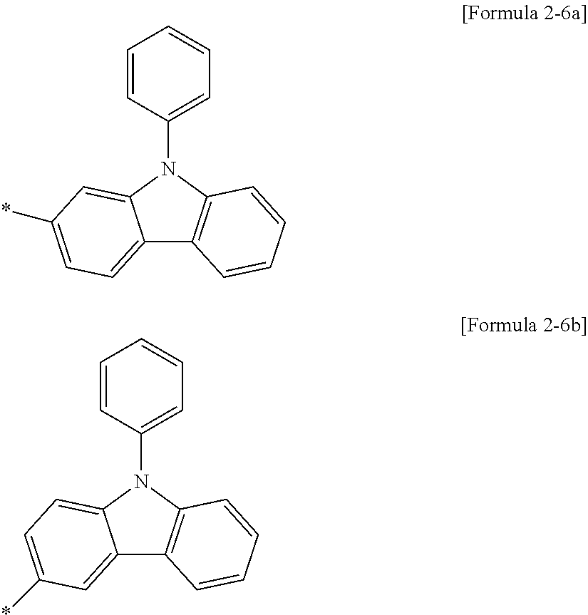


| TABLE 3 | ||||
| No. | Subsituent structure | |||
| 1 |
|
|||
| 2 |
|
|||
| 3 |
|
|||
| 4 |
 |
|||
| 5 |
 |
|||
| 6 |
 |
|||
| 7 |
 |
|||
| 8 |
 |
|||
| 9 |
 |
|||
| 10 |
 |
|||
| 11 |
 |
|||


| TABLE 4 | |
| No. | Structure |
| 1 |
 |
| 2 |
 |
| 3 |
 |
| 4 |
 |
| 5 |
 |
| 6 |
 |
| 7 |
 |
| 8 |
 |
| 9 |
 |
| 10 |
 |
| 11 |
 |
| 12 |
 |
| 13 |
 |
| 14 |
 |
| 15 |
 |
| 16 |
 |
| 17 |
 |
| 18 |
 |
| 19 |
 |
| 20 |
 |
| 21 |
 |
| 22 |
 |
| 23 |
 |
| 24 |
 |
| 25 |
 |
| 26 |
 |
| 27 |
 |
| 28 |
 |
| 29 |
 |
| 30 |
 |
| 31 |
 |
| 32 |
 |
| 33 |
 |
| 34 |
 |
| 35 |
 |
| 36 |
 |
| 37 |
 |
| 38 |
 |
| 39 |
 |
| 40 |
 |
| 41 |
 |
| 42 |
 |
| 43 |
 |
| 44 |
 |
| 45 |
 |
| 46 |
 |
| 47 |
 |
| 48 |
 |
| 49 |
 |
| 50 |
 |
| 51 |
 |
| 52 |
 |
| 53 |
 |
| 54 |
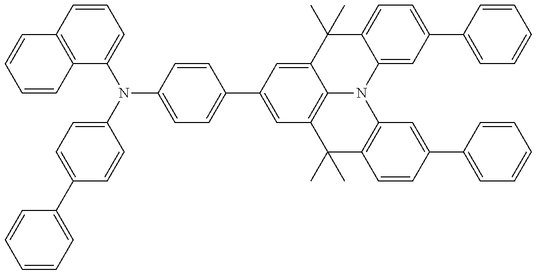 |
| 55 |
 |
| 56 |
 |
| 57 |
 |
| 58 |
 |
| 59 |
 |
| 60 |
 |
| 61 |
 |
| 62 |
 |
| 63 |
 |
| 64 |
 |
| 65 |
 |
| 66 |
 |
| 67 |
 |
| 68 |
 |
| 69 |
 |
| 70 |
 |
| 71 |
 |
| 72 |
 |
| 73 |
 |
| 74 |
 |
| 75 |
 |
| 76 |
 |
| 77 |
 |
| 78 |
 |
| 79 |
 |
| 80 |
 |
| 81 |
 |
| 82 |
 |
| 83 |
 |
| 84 |
 |
| 85 |
 |
| 86 |
 |
| 87 |
 |
| 88 |
 |
| 89 |
 |
| 90 |
 |
| 91 |
 |
| 92 |
 |
| 93 |
 |
| 94 |
 |
| 95 |
 |
| 96 |
 |
| 97 |
 |
| 98 |
 |
| 99 |
 |
| 100 |
 |
| 101 |
 |
| 102 |
 |
| 103 |
 |
| 104 |
 |
| 105 |
 |
| 106 |
 |
| 107 |
 |
| 108 |
 |
| 109 |
 |
| 110 |
 |
| 111 |
 |
| 112 |
 |
| 113 |
 |
| 114 |
 |
| 115 |
 |
| 116 |
 |
| 117 |
 |
| 118 |
 |
| 119 |
 |
| 120 |
 |


P1/P2≥1 [Equation 1]
In Equation 1,


| TABLE 5 | ||
| Power efficiency | Lifespan | |
| Element No. | [lm/W] | (T75@85° C. [hr]) |
| Light-Emitting Element A-1 | 20.7 | 419 |
| Light-Emitting Element A-2 | 28.5 | 603 |
| Light-Emitting Element A-3 | 26.7 | 624 |
| Light-Emitting Element A-4 | 29.5 | 579 |
| Light-Emitting Element A-5 | 24.6 | 500 |
| Light-Emitting Element A-6 | 21.1 | 426 |
| Light-Emitting Element A-7 | 20.8 | 430 |
| Light-Emitting Element A-8 | 16.3 | 357 |
| Light-Emitting Element A-9 | 13.5 | 301 |
| Light-Emitting Element A-10 | 17.3 | 385 |
| Comparative Element 1 | 9.2 | 227 |
| Comparative Element 2 | 10.8 | 224 |
| Comparative Element 3 | 8.8 | 218 |
| TABLE 6 | ||
| Power efficiency | Lifespan | |
| Element No. | [lm/W] | (T75@85° C. [hr]) |
| Light-Emitting Element B-1 | 32.4 | 655 |
| Light-Emitting Element B-2 | 28.5 | 683 |
| Light-Emitting Element B-3 | 26.7 | 567 |
| Light-Emitting Element B-4 | 24.6 | 615 |
| Comparative Element 4 | 9.3 | 199 |
| TABLE 7 | ||
| Power efficiency | Lifespan | |
| Element No. | [lm/W] | (T75@85° C. [hr]) |
| Light-Emitting Element C-1 | 33.5 | 586 |
| Light-Emitting Element C-2 | 29.5 | 562 |
| Light-Emitting Element C-3 | 17.9 | 413 |
| Light-Emitting Element C-4 | 19.5 | 447 |
| Comparative Element 5 | 9.6 | 193 |
| TABLE 8 | ||
| Power efficiency | Lifespan | |
| Element No. | [lm/W] | (T75@85° C. [hr]) |
| Light-Emitting Element D-1 | 21.4 | 396 |
| Light-Emitting Element D-2 | 19.6 | 372 |
| Light-Emitting Element D-3 | 21.3 | 343 |
| Light-Emitting Element D-4 | 22.7 | 430 |
| Comparative Element 6 | 11.2 | 213 |
| TABLE 9 | ||
| Power efficiency | Lifespan | |
| Element No. | [lm/W] | (T75@85° C. [hr]) |
| Light-Emitting Element E-1 | 32.8 | 701 |
| Light-Emitting Element E-2 | 30.7 | 730 |
| Light-Emitting Element E-3 | 34.0 | 658 |
| Light-Emitting Element E-4 | 28.3 | 606 |
| Comparative Element 7 | 10.7 | 206 |
Claims (9)


Applications Claiming Priority (3)
| Application Number | Priority Date | Filing Date | Title |
|---|---|---|---|
| KR10-2012-0136377 | 2012-11-28 | ||
| KR1020120136377A KR101468088B1 (en) | 2012-11-28 | 2012-11-28 | Novel compound, light-emitting device including the compound and electronic device |
| PCT/KR2013/010886 WO2014084619A1 (en) | 2012-11-28 | 2013-11-28 | Novel compound, and light-emitting element and electronic device comprising same |
Publications (2)
| Publication Number | Publication Date |
|---|---|
| US20160248019A1 US20160248019A1 (en) | 2016-08-25 |
| US10050208B2 true US10050208B2 (en) | 2018-08-14 |
Family
ID=50828175
Family Applications (1)
| Application Number | Title | Priority Date | Filing Date |
|---|---|---|---|
| US14/647,582 Active 2034-11-10 US10050208B2 (en) | 2012-11-28 | 2013-11-28 | Compound, and light-emitting element and electronic device comprising same |
Country Status (3)
| Country | Link |
|---|---|
| US (1) | US10050208B2 (en) |
| KR (1) | KR101468088B1 (en) |
| WO (1) | WO2014084619A1 (en) |
Families Citing this family (7)
| Publication number | Priority date | Publication date | Assignee | Title |
|---|---|---|---|---|
| KR101503431B1 (en) * | 2013-01-30 | 2015-03-17 | 주식회사 엘엠에스 | Novel compound, light-emitting device including the compound and electronic device |
| KR101790550B1 (en) * | 2014-08-13 | 2017-10-26 | (주)피엔에이치테크 | An electroluminescent compound and an electroluminescent device comprising the same |
| US20160248030A1 (en) * | 2014-09-04 | 2016-08-25 | Boe Technology Group Co., Ltd. | Organic electroluminescent display deivce, a fabricating method thereof and a display device |
| KR102408822B1 (en) * | 2014-11-27 | 2022-06-15 | 삼성디스플레이 주식회사 | Monoamine derivative and organic electroluminescece device including the same |
| JP7073388B2 (en) * | 2016-11-08 | 2022-05-23 | メルク パテント ゲーエムベーハー | Compounds for electronic devices |
| CN106549113B (en) * | 2017-01-16 | 2019-10-01 | 上海天马有机发光显示技术有限公司 | A kind of organic light emitting display panel and device |
| KR102508497B1 (en) | 2018-03-26 | 2023-03-10 | 삼성디스플레이 주식회사 | Heterocyclic compound and organic light emitting device comprising the same |
Citations (4)
| Publication number | Priority date | Publication date | Assignee | Title |
|---|---|---|---|---|
| KR20100006072A (en) | 2008-07-08 | 2010-01-18 | 주식회사 하나화인켐 | Organic light emitting compound and organic light emitting device comprising the same |
| WO2010050778A1 (en) * | 2008-10-31 | 2010-05-06 | Gracel Display Inc. | Novel compounds for organic electronic material and organic electronic device using the same |
| WO2011107186A2 (en) | 2010-03-02 | 2011-09-09 | Merck Patent Gmbh | Compounds for electronic devices |
| KR20110106192A (en) | 2010-03-22 | 2011-09-28 | 에스에프씨 주식회사 | Condensed arylamine compound and organic light emitting device comprising the same |
-
2012
- 2012-11-28 KR KR1020120136377A patent/KR101468088B1/en active Active
-
2013
- 2013-11-28 WO PCT/KR2013/010886 patent/WO2014084619A1/en not_active Ceased
- 2013-11-28 US US14/647,582 patent/US10050208B2/en active Active
Patent Citations (6)
| Publication number | Priority date | Publication date | Assignee | Title |
|---|---|---|---|---|
| KR20100006072A (en) | 2008-07-08 | 2010-01-18 | 주식회사 하나화인켐 | Organic light emitting compound and organic light emitting device comprising the same |
| WO2010050778A1 (en) * | 2008-10-31 | 2010-05-06 | Gracel Display Inc. | Novel compounds for organic electronic material and organic electronic device using the same |
| KR20100048447A (en) | 2008-10-31 | 2010-05-11 | 다우어드밴스드디스플레이머티리얼 유한회사 | Novel compounds for organic electronic material and organic electronic device using the same |
| WO2011107186A2 (en) | 2010-03-02 | 2011-09-09 | Merck Patent Gmbh | Compounds for electronic devices |
| US20120319052A1 (en) | 2010-03-02 | 2012-12-20 | Merck Patent Gmbh | Compounds for electronic devices |
| KR20110106192A (en) | 2010-03-22 | 2011-09-28 | 에스에프씨 주식회사 | Condensed arylamine compound and organic light emitting device comprising the same |
Also Published As
| Publication number | Publication date |
|---|---|
| KR101468088B1 (en) | 2014-12-05 |
| WO2014084619A1 (en) | 2014-06-05 |
| KR20140068643A (en) | 2014-06-09 |
| US20160248019A1 (en) | 2016-08-25 |
Similar Documents
| Publication | Publication Date | Title |
|---|---|---|
| US11877464B2 (en) | Organic light emitting element | |
| US10050208B2 (en) | Compound, and light-emitting element and electronic device comprising same | |
| US9966538B2 (en) | Compound, light-emitting element and electronic device comprising same | |
| US10522764B2 (en) | Compound, light-emitting element comprising same and electronic device comprising the light-emitting element | |
| CN103137879B (en) | Organic light-emitting diode including multi-layered hole transporting layer, and flat display device | |
| US11952372B2 (en) | Tribenzazole amine derivative and organic electroluminescent device comprising same | |
| US10862044B2 (en) | Organic compound and light emitting diode and organic light emitting diode display device using the same | |
| US10141519B2 (en) | Compound, light emitting device comprising same, and electronic device | |
| US11177443B2 (en) | Compound and light emitting diode including same | |
| US9711734B2 (en) | Organic light-emitting device | |
| US11723268B2 (en) | Organic light-emitting element | |
| US20140145154A1 (en) | Organic light-emitting device | |
| US20160072077A1 (en) | Organic light emitting diode and organic light emitting display device including the same | |
| US20230337527A1 (en) | Organic compound and organic electroluminescent device comprising same | |
| US20090015150A1 (en) | Organic light emitting device and method for manufacturing the same | |
| TW202210611A (en) | Organic electronic device comprising a compound of formula (i), display device comprising the organic electronic device as well as compounds of formula (i) for use in organic electronic devices | |
| US9614163B2 (en) | Light-emitting diode having novel structure and electronic apparatus comprising same | |
| US20190280216A1 (en) | Organic electroluminescent element, display and lighting device | |
| KR101468087B1 (en) | Novel compound, light-emitting device including the compound and electronic device | |
| US10741770B2 (en) | Compounds comprising triazine group, fluorene-group and hetero-fluorene group | |
| KR101411594B1 (en) | Novel compound, light-emitting device including the compound and electronic device | |
| US9853222B2 (en) | Condensed-cyclic compound and organic light-emitting diode comprising the same | |
| US9741935B2 (en) | Organic light-emitting device | |
| US20140151650A1 (en) | Heterocyclic compound and organic light-emitting device including the same | |
| US9755153B2 (en) | Organic compound and organic light emitting diode device including the same |
Legal Events
| Date | Code | Title | Description |
|---|---|---|---|
| AS | Assignment |
Owner name: LMS CO., LTD, KOREA, REPUBLIC OF Free format text: ASSIGNMENT OF ASSIGNORS INTEREST;ASSIGNORS:CHOI, JEONG OG;JUNG, JOON HO;KWON, OH KWAN;REEL/FRAME:035721/0832 Effective date: 20150417 |
|
| STCF | Information on status: patent grant |
Free format text: PATENTED CASE |
|
| MAFP | Maintenance fee payment |
Free format text: PAYMENT OF MAINTENANCE FEE, 4TH YR, SMALL ENTITY (ORIGINAL EVENT CODE: M2551); ENTITY STATUS OF PATENT OWNER: SMALL ENTITY Year of fee payment: 4 |
|
| MAFP | Maintenance fee payment |
Free format text: PAYMENT OF MAINTENANCE FEE, 8TH YR, SMALL ENTITY (ORIGINAL EVENT CODE: M2552); ENTITY STATUS OF PATENT OWNER: SMALL ENTITY Year of fee payment: 8 |