US10049705B2 - Memories having select devices between access lines and in memory cells formed of a same type of circuit element - Google Patents
Memories having select devices between access lines and in memory cells formed of a same type of circuit element Download PDFInfo
- Publication number
- US10049705B2 US10049705B2 US15/656,690 US201715656690A US10049705B2 US 10049705 B2 US10049705 B2 US 10049705B2 US 201715656690 A US201715656690 A US 201715656690A US 10049705 B2 US10049705 B2 US 10049705B2
- Authority
- US
- United States
- Prior art keywords
- select device
- memory
- access line
- line
- select
- Prior art date
- Legal status (The legal status is an assumption and is not a legal conclusion. Google has not performed a legal analysis and makes no representation as to the accuracy of the status listed.)
- Active, expires
Links
Images


Classifications
-
- G—PHYSICS
- G11—INFORMATION STORAGE
- G11C—STATIC STORES
- G11C5/00—Details of stores covered by group G11C11/00
- G11C5/06—Arrangements for interconnecting storage elements electrically, e.g. by wiring
-
- G—PHYSICS
- G11—INFORMATION STORAGE
- G11C—STATIC STORES
- G11C13/00—Digital stores characterised by the use of storage elements not covered by groups G11C11/00, G11C23/00, or G11C25/00
- G11C13/0002—Digital stores characterised by the use of storage elements not covered by groups G11C11/00, G11C23/00, or G11C25/00 using resistive RAM [RRAM] elements
- G11C13/0021—Auxiliary circuits
- G11C13/0023—Address circuits or decoders
-
- G—PHYSICS
- G11—INFORMATION STORAGE
- G11C—STATIC STORES
- G11C13/00—Digital stores characterised by the use of storage elements not covered by groups G11C11/00, G11C23/00, or G11C25/00
- G11C13/0002—Digital stores characterised by the use of storage elements not covered by groups G11C11/00, G11C23/00, or G11C25/00 using resistive RAM [RRAM] elements
- G11C13/0021—Auxiliary circuits
- G11C13/003—Cell access
-
- G—PHYSICS
- G11—INFORMATION STORAGE
- G11C—STATIC STORES
- G11C7/00—Arrangements for writing information into, or reading information out from, a digital store
- G11C7/18—Bit line organisation; Bit line lay-out
-
- G—PHYSICS
- G11—INFORMATION STORAGE
- G11C—STATIC STORES
- G11C2213/00—Indexing scheme relating to G11C13/00 for features not covered by this group
- G11C2213/70—Resistive array aspects
- G11C2213/72—Array wherein the access device being a diode
Definitions
- the present embodiments relate generally to memory and a particular embodiment relates to variable resistance memory devices.
- Flash memory devices have developed into a popular source of non-volatile memory for a wide range of electronic applications. Flash memory devices typically use a one-transistor memory cell that allows for high memory densities, high reliability, and low power consumption. Common uses for flash memory include personal computers, flash drives, digital cameras, and cellular telephones. Program code and system data such as a basic input/output system (BIOS) are typically stored in flash memory devices for use in personal computer systems.
- BIOS basic input/output system
- Flash memory density has increased and cost per bit has decreased in recent years. To increase density, memory cell size and proximity to adjacent memory cells have been reduced. This can lead to problems with disturb conditions resulting from interaction between adjacent memory cells. Additionally, flash memory is still relatively slow when compared to other forms of memory (e.g., DRAM).
- Variable resistance memory such as resistive random access memory (RRAM) is a memory technology that provides a non-volatile memory function in a variable resistance memory cell. For example, a low resistance of the memory cell indicates one state while a high resistance indicates a second state.
- variable resistance memory includes metal oxide, phase change (GST), nano-filament, stiction force, mechanical deformation, polymer, molecular, conductive bridge, and MRAM.
- FIG. 1 shows a typical cross point resistive RAM array, with a select device and a programmable element in series forming each cell at an intersection of a pair of access lines, which are referred to herein as bit lines and word lines, but which for the purposes of a RRAM are interchangeable.
- the select device is a non-ohmic device, such as a diode.
- a typical core cell size for RRAM cells is 4F 2 . That is, with F as the smallest feature size, the area of an RRAM cell on a die, including any overhead and spacing, is 2F by 2F, or 4F 2 .
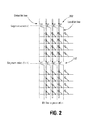
- bit lines and word lines cannot span an entire length and width of a memory. Connected to in this context includes, but is not limited to, being electrically connected to, whether directly or indirectly through an intervening component or components. Therefore, bit line and word line segmentation is used as is shown in FIG. 2 .
- segmentation transistors such as transistors 202 are used. The segmentation transistors 202 are used to divide the array into smaller sections. It is difficult to fabricate small transistors, and it is difficult to tightly pack transistors. Further, as cells continue to scale smaller and smaller, transistors do not become smaller at the same rate. Segmentation transistors such as transistors 202 are far larger than the 4F 2 size of typical RRAM cells, and as the density of arrays continues to increase, large segmentation transistors take up an increasing percentage of die space, reducing efficiency of the array.
- FIG. 1 is a portion of a typical RRAM memory array
- FIG. 2 is a portion of a segmented typical RRAM memory array
- FIG. 3 is a partial circuit diagram of an RRAM memory array according to an embodiment of the present disclosure.
- FIG. 4 is a partial circuit diagram of an RRAM memory array according to another embodiment of the present disclosure.
- FIG. 5 is a diagram showing operation of a portion of the RRAM memory array of FIG. 3 ;
- FIG. 6 is a voltage/current curve for the operation of the RRAM memory array of FIG. 5 ;
- FIG. 7 is a diagram showing another operation of a portion of the RRAM memory array of FIG. 3 ;
- FIG. 8 is a voltage/current curve for the operation of the RRAM memory array of FIG. 7 ;
- FIG. 9 is a flow chart diagram of a method according to an embodiment of the present disclosure.
- FIG. 10 is a block diagram of one embodiment of a memory system that can incorporate the memory array of FIG. 3 or 4 .
- Cross point RRAM array cells are a two tier stack of components.
- an RRAM array cell comprises a programmable element (e.g., a variable resistive element) that is usually either over or under a select device.
- the variable resistive element changes states, and the different states represent a programmed cell and an erased cell.
- the select device is used for the purpose of selecting the particular cell of interest in the array.
- a cross point array is so named because the access lines, referred to as bit lines and word lines, of the array cross at 90 degree angles, for example, forming a compact efficient array having a small area.
- the bit lines and word lines are typically sized as small as equipment can make them, and the spacing between adjacent bit lines and between adjacent word lines is also typically as small.
- bit lines are shown in the figures in a vertical direction, and word lines are shown in the figures in a horizontal direction.
- bit lines and word lines each function the same. That is, what are typically referred to as bit lines and word lines are in fact interchangeable in RRAM. Functionally, bit lines and word lines may be referred to generally as access lines.
- a string of memory cells is defined herein to be a group of memory cells that are each connected to a common access line, e.g., a group of memory cells each connected to a local bit line, with each local bit line connected to a global bit line by a segmentation element, a group of memory cells each connected to a local word line, with each local word line connected to a global word line by a segmentation element, or a group of memory cells each connected to a global access line.
- the select device of a variable resistance memory cell is typically a diode. Since there are numerous types of variable resistive elements, in some RRAM memories the select devices may be uni-directional diodes, and in other RRAM memories the select devices may be bi-directional diodes. When bi-directional diodes are used as select devices, they may be symmetrical or non-symmetrical, that is, forward and reverse turn-on voltages for a non-symmetric bi-directional diode may be different.
- the choice of the programmable element typically dictates the choice of the select device. For example, a phase change memory may have all of its current flow in one direction, and as such, use a uni-directional select device. Conductive bridge memory may use current flow in different directions for programming and erasing, and as such, use a bi-directional select device.
- FIG. 3 A portion of a memory array 300 according to an embodiment of the disclosure is shown in FIG. 3 .
- Array 300 comprises a plurality of blocks 302 divided by segmentation elements 304 .
- Segmentation elements 304 comprise diodes in one embodiment, and may be identical to the select device for each variable resistance memory cell 312 .
- Global bit lines 306 span multiple blocks, and are connected to local bit lines 308 of the blocks 302 by the segmentation elements 304 for the particular block.
- Word lines 310 which may be local word lines or global word lines, cross the local bit lines 308 , and a variable resistance cell 312 is connected between each local bit line 308 and its crossing word line 310 .
- Variable resistance cells comprise a select device (e.g., a diode) in series with a programmable element.
- a pair of biasing lines 314 and 316 are also connected to the local bit lines 308 and run, in one embodiment, parallel to word lines 310 .
- Each of the biasing lines 314 , 316 is connected to a local bit line 308 by a respective bias device 318 , 320 , which comprises a select device, like a memory cell, but unlike a memory cell, does not include a programmable element.
- Biasing line 314 is connected to a plurality of local bit lines 308 by a plurality of biasing devices 318 , each biasing device 318 connected between the line 314 and a respective one of the local bit lines 308 in one direction
- biasing line 316 is connected to a plurality of local bit lines 308 by a plurality of biasing devices 320 , each biasing device 320 connected between the line 316 and a respective one of the local bit lines 308 , in the opposite direction.
- the biasing devices 318 and 320 are uni-directional diodes, current flow for biasing devices 318 flows from line 314 to the local bit lines 308 , and current flow for biasing devices 320 flows from the local bit lines 308 to line 316 .
- the biasing lines can be used to forward or reverse bias the local bit lines for selecting or unselecting specific local bit lines.
- the biasing devices and segmentation elements do use area in an array. Compared to the size of segmentation transistors, however, the area used by the biasing devices and segmentation elements combined is much smaller for each global bit line than by transistors. Further, the biasing devices and segmentation elements will scale with the memory cells, whereas transistors do not scale with the memory cells.
- the segmentation elements are in one embodiment the same elements as are used for the select devices for the variable resistance memory cells. Compared to segmentation transistors, the segmentation elements 304 are much smaller in size, are much easier to fabricate, and can scale with the cells themselves. That is, as cell size decreases, the segmentation element size will also decrease, saving both cost and die area. As word lines and bit lines are interchangeable in RRAM, the segmentation of the array may be performed on either or both of the sets of bit lines and word lines without departing from the scope of the disclosure.
- segmenting from a global bit line to a regional bit line, and then to a local bit line may be used.
- the same sub-segmenting may also be used for word lines.
- FIG. 4 shows an array 300 as in FIG. 3 , except using two segmentation elements 402 in parallel between global bit lines 306 and local bit lines 308 instead of a single segmentation element 304 .
- a segmentation element of the same size as the select devices in the array may not be able to conduct enough current to operate the string of cells. It should be understood that the number of segmentation elements placed in parallel between the global bit lines and local bit lines may increase without departing from the scope of the disclosure.
- Programming or erasing a variable resistance memory cell comprises applying a forward or reverse bias across it.
- the differences between read, program, and erase operations are determined by the cell itself, and voltage and/or current magnitude, duration, bias (reverse or forward), and timing and/or waveform.
- Some variable resistance memory cells use bi-directional current flow for operation, and some use uni-directional current flow. What distinguishes them is the waveform.
- the select device is uni-directional, and for bi-directional cells, the select device is bi-directional.
- FIGS. 5-8 Forward and reverse biasing cells for operation is shown in greater detail in FIGS. 5-8 .
- FIGS. 5 and 6 show forward biasing of selected cells in selected and unselected blocks
- FIGS. 7 and 8 show reverse biasing of selected cells in selected and unselected blocks. Methods are further described with respect to FIGS. 9 and 10 .
- Appropriate voltages for forward and reverse biasing cells will vary depending upon, e.g., the turn-on voltage of the select devices, the leakage tolerance for the array, and the size and characteristics of the cells and the select devices.
- voltages that are sufficient to turn on the select device for a selected cell, and to reduce leakage or turn off select devices for unselected cells and blocks are chosen.
- Diodes can leak current when a bias below a turn-on voltage is applied to them. The amount of leakage depends on the actual voltage applied, and voltages in one embodiment are chosen to keep unselected diodes off or to keep the leakage below an acceptable amount, the acceptable amount determined by the application of the array.
- FIG. 5 two blocks, selected block 502 and unselected block 504 , are shown.
- Cells 506 and 508 are selected cells.
- the bit lines and word lines that intersect at those cells have a voltage applied to them that is sufficient to forward bias the select device of the cell.
- global bit lines 306 1 and 306 3 which connect to local bit lines 308 1 and 308 3 through segmentation elements 304 1 and 304 3 , are biased at a bit line select voltage Vblsel sufficient to turn on the segmentation elements and select devices (Vf).
- Unselected bit lines 306 2 and 306 4 are biased at a bit line unselect voltage Vblunsel.
- Vblunsel is chosen in one embodiment to reduce leakage to an acceptable level for the function of the array, and/or to reduce stress on the segmentation elements connected to unselected bit lines, and/or to ensure reverse biasing of the segmentation elements and/or the select devices connected to unselected bit lines.
- the selected word line 310 2 is biased at a word line select voltage Vwsel, in one embodiment a reference voltage (e.g., 0 or ground), and unselected word lines are biased at a word line unselect voltage Vwlunsel, chosen the same way as the bit line unselect voltages are chosen, that is what is appropriate to turn the unselected select devices off or to reverse bias them.
- the biasing lines 314 and 316 in the selected block 502 are also biased with Vwlunsel, so that the select devices of unselected cells in the selected block remain turned off.
- word lines are left floating, and the forward bias voltage Vf is applied to the biasing lines.
- Vf minus a threshold voltage of biasing devices 318 on the local bit lines, and keeps segmentation elements 304 of the unselected block 504 off.
- a voltage versus current curve for FIG. 5 is shown in FIG. 6 .
- FIG. 7 two blocks, selected block 702 and unselected block 704 , are shown.
- Cells 706 and 708 are selected cells.
- the forward bias conditions from FIG. 5 can be reversed.
- FIG. 5 had a reference voltage (e.g., 0 or ground)
- a reverse bias voltage Vr is applied.
- the bit lines and word lines that intersect at those cells have a voltage applied to them that is sufficient to reverse bias the select device of the cell.
- global bit lines 306 1 and 306 3 which connect to local bit lines 308 1 and 308 3 through segmentation elements 304 1 and 304 3 , are biased at a bit line select voltage Vblsel of a reference voltage (e.g., 0 or ground) sufficient to reverse bias the segmentation elements and select devices.
- Unselected bit lines 306 2 and 306 4 are biased at a bit line unselect voltage Vblunsel.
- Vblunsel is chosen in one embodiment to reduce leakage to an acceptable level for the function of the array, and/or to reduce stress on the segmentation elements connected to unselected bit lines, and/or to ensure reverse biasing of the segmentation elements and/or the select devices connected to unselected bit lines.
- the selected word line 310 2 is biased at a word line select voltage Vwsel, in one embodiment a reverse bias voltage Vr, and unselected word lines are biased at a word line unselect voltage Vwlunsel, chosen the same way as the bit line unselect voltages are chosen, that is what is appropriate to turn the unselected select devices off or to reverse bias them.
- the biasing lines 314 and 316 in the selected block 702 are also biased with Vwlunsel, so that the select devices of unselected cells in the selected block remain turned off.
- word line unselect voltage Vwlunsel is applied to all word lines and to the biasing lines 314 and 316 , sufficient to keep segmentation elements 304 in unselected block 704 off.
- a voltage versus current curve for FIG. 7 is shown in FIG. 8 .
- Method 900 comprises biasing a two terminal segmentation element for selected cells of a selected block of the memory to turn the segmentation element on in block 902 , biasing a two terminal segmentation element for unselected cells of a selected block of the memory to turn the segmentation element off in block 904 , and biasing segmentation elements for unselected blocks of the memory to turn the segmentation elements off in block 906 .
- a pair of biasing lines in the array may be biased to reverse bias select devices of unselected cells of the memory, or may be biased to apply nearly any bias to unselected cells of the memory and to local access lines of the memory.
- biasing the segmentation element comprises biasing a diode connected between a global access line of the memory and a local access line of the memory.
- Reverse biasing segmentation elements for unselected blocks of the memory comprises in one embodiment biasing a plurality of diodes, each diode connected between a biasing line and a respective local access line.
- FIG. 10 illustrates a functional block diagram of a memory 1000 .
- the memory 1000 is coupled to an external processor 1010 .
- the processor 1010 may be a microprocessor or some other type of controller.
- the memory 1000 and the processor 1010 form part of a memory system 1020 .
- the memory 1000 has been simplified to focus on features of the memory that are helpful in understanding the present embodiments.
- the memory 1000 includes an array 1030 of memory devices such as the arrays of FIGS. 3 and 4 .
- the memory array 1030 may be arranged in banks of word line rows and bit line columns. In one embodiment, the columns of the memory array 1030 comprise series strings of memory devices 210 .
- Address buffer circuitry 1040 is provided to latch address signals provided through I/O circuitry 1060 . Address signals are received and decoded by a row decoder 1044 and a column decoder 1046 to access the memory array 1030 . It will be appreciated by those skilled in the art with the benefit of the present description that the number of address input connections depends on the density and architecture of the memory array 1030 . That is, the number of addresses increases with both increased memory cell counts and increased bank and block counts.
- the memory 1000 reads data in the memory array 1030 by sensing voltage or current changes in the memory array columns using sense amplifier circuitry 1050 .
- the sense amplifier circuitry 1050 in one embodiment, is coupled to read and latch a row of data from the memory array 1030 .
- Data input and output buffer circuitry 1060 is included for bidirectional data communication as well as the address communication over a plurality of data connections 1062 with the controller 1010 .
- Write circuitry 1055 is provided to write data to the memory array.
- Memory control circuitry 1070 decodes signals provided on control connections 1072 from the processor 1010 . These signals are used to control the operations on the memory array 1030 , including data read, data write (program), and erase operations.
- the memory control circuitry 1070 may be a state machine, a sequencer, or some other type of controller to generate the memory control signals. In one embodiment, the memory control circuitry 1070 is configured to control the timing and generation of voltages for the methods for sensing, programming, and erasing of memory cells.
- FIG. 10 has been simplified to facilitate a basic understanding of the features of the memory. A more detailed understanding of internal circuitry and functions of resistive memories are known to those skilled in the art.
- one or more embodiments provide a memory array with segmentation.
- the segmentation elements scale with the memory cells, and may be uni-directional or bi-directional diodes. Biasing lines in the array allow biasing of selected and unselected select devices and segmentation elements with any desired bias.
Abstract
Description
Claims (20)
Priority Applications (3)
| Application Number | Priority Date | Filing Date | Title |
|---|---|---|---|
| US15/656,690 US10049705B2 (en) | 2012-08-29 | 2017-07-21 | Memories having select devices between access lines and in memory cells formed of a same type of circuit element |
| US16/039,559 US10249345B2 (en) | 2012-08-29 | 2018-07-19 | Memories having select devices between access lines and in memory cells |
| US16/188,957 US10418072B2 (en) | 2012-08-29 | 2018-11-13 | Memories having select devices between access lines and in memory cells |
Applications Claiming Priority (3)
| Application Number | Priority Date | Filing Date | Title |
|---|---|---|---|
| US13/597,917 US8929120B2 (en) | 2012-08-29 | 2012-08-29 | Diode segmentation in memory |
| US14/570,254 US9721622B2 (en) | 2012-08-29 | 2014-12-15 | Systems with memory segmentation and systems with biasing lines to receive same voltages during accessing |
| US15/656,690 US10049705B2 (en) | 2012-08-29 | 2017-07-21 | Memories having select devices between access lines and in memory cells formed of a same type of circuit element |
Related Parent Applications (1)
| Application Number | Title | Priority Date | Filing Date |
|---|---|---|---|
| US14/570,254 Continuation US9721622B2 (en) | 2012-08-29 | 2014-12-15 | Systems with memory segmentation and systems with biasing lines to receive same voltages during accessing |
Related Child Applications (1)
| Application Number | Title | Priority Date | Filing Date |
|---|---|---|---|
| US16/039,559 Continuation US10249345B2 (en) | 2012-08-29 | 2018-07-19 | Memories having select devices between access lines and in memory cells |
Publications (2)
| Publication Number | Publication Date |
|---|---|
| US20170323668A1 US20170323668A1 (en) | 2017-11-09 |
| US10049705B2 true US10049705B2 (en) | 2018-08-14 |
Family
ID=50184200
Family Applications (5)
| Application Number | Title | Priority Date | Filing Date |
|---|---|---|---|
| US13/597,917 Active 2033-01-08 US8929120B2 (en) | 2012-08-29 | 2012-08-29 | Diode segmentation in memory |
| US14/570,254 Active 2032-09-10 US9721622B2 (en) | 2012-08-29 | 2014-12-15 | Systems with memory segmentation and systems with biasing lines to receive same voltages during accessing |
| US15/656,690 Active 2032-09-11 US10049705B2 (en) | 2012-08-29 | 2017-07-21 | Memories having select devices between access lines and in memory cells formed of a same type of circuit element |
| US16/039,559 Active US10249345B2 (en) | 2012-08-29 | 2018-07-19 | Memories having select devices between access lines and in memory cells |
| US16/188,957 Active US10418072B2 (en) | 2012-08-29 | 2018-11-13 | Memories having select devices between access lines and in memory cells |
Family Applications Before (2)
| Application Number | Title | Priority Date | Filing Date |
|---|---|---|---|
| US13/597,917 Active 2033-01-08 US8929120B2 (en) | 2012-08-29 | 2012-08-29 | Diode segmentation in memory |
| US14/570,254 Active 2032-09-10 US9721622B2 (en) | 2012-08-29 | 2014-12-15 | Systems with memory segmentation and systems with biasing lines to receive same voltages during accessing |
Family Applications After (2)
| Application Number | Title | Priority Date | Filing Date |
|---|---|---|---|
| US16/039,559 Active US10249345B2 (en) | 2012-08-29 | 2018-07-19 | Memories having select devices between access lines and in memory cells |
| US16/188,957 Active US10418072B2 (en) | 2012-08-29 | 2018-11-13 | Memories having select devices between access lines and in memory cells |
Country Status (4)
| Country | Link |
|---|---|
| US (5) | US8929120B2 (en) |
| CN (1) | CN104603883B (en) |
| TW (1) | TWI520135B (en) |
| WO (1) | WO2014035874A1 (en) |
Families Citing this family (7)
| Publication number | Priority date | Publication date | Assignee | Title |
|---|---|---|---|---|
| US9361975B2 (en) * | 2013-03-11 | 2016-06-07 | Adesto Technologies Corporation | Sensing data in resistive switching memory devices |
| US9530469B2 (en) * | 2013-03-15 | 2016-12-27 | Sony Semiconductor Solutions Corporation | Integrated circuit system with non-volatile memory stress suppression and method of manufacture thereof |
| US9123392B1 (en) * | 2014-03-28 | 2015-09-01 | Sandisk 3D Llc | Non-volatile 3D memory with cell-selectable word line decoding |
| US9972397B2 (en) * | 2016-06-24 | 2018-05-15 | SK Hynix Inc. | Semiconductor memory device and operating method thereof |
| US9887004B2 (en) | 2016-06-28 | 2018-02-06 | Western Digital Technologies, Inc. | Bi-directional RRAM decoder-driver |
| KR102634322B1 (en) * | 2016-10-10 | 2024-02-07 | 삼성전자주식회사 | Variable ressitance memory device compensating bidirectional switch, memory system and operation method thereof |
| US11302634B2 (en) | 2020-02-13 | 2022-04-12 | Micron Technology, Inc. | Microelectronic devices with symmetrically distributed staircase stadiums and related systems and methods |
Citations (17)
| Publication number | Priority date | Publication date | Assignee | Title |
|---|---|---|---|---|
| US4747083A (en) | 1983-06-29 | 1988-05-24 | Fujitsu Limited | Semiconductor memory with segmented word lines |
| US5781469A (en) | 1997-01-24 | 1998-07-14 | Atmel Corporation | Bitline load and precharge structure for an SRAM memory |
| US20050180203A1 (en) | 2004-02-16 | 2005-08-18 | Taiwan Semiconductor Manufacturing Co., Ltd. | Segmented MRAM memory array |
| US7002825B2 (en) | 2003-03-31 | 2006-02-21 | Matrix Semiconductor, Inc. | Word line arrangement having segmented word lines |
| US7054219B1 (en) | 2005-03-31 | 2006-05-30 | Matrix Semiconductor, Inc. | Transistor layout configuration for tight-pitched memory array lines |
| WO2007008699A2 (en) | 2005-07-11 | 2007-01-18 | Sandisk 3D Llc | Apparatus and method for reading an array of nonvolatile memory cells including switchable resistor memory elements |
| US20090141535A1 (en) | 2005-07-01 | 2009-06-04 | Sandisk 3D Llc | Methods involving memory with high dielectric constant antifuses adapted for use at low voltage |
| US7733685B2 (en) | 2008-07-09 | 2010-06-08 | Sandisk 3D Llc | Cross point memory cell with distributed diodes and method of making same |
| US20100238697A1 (en) | 2008-02-19 | 2010-09-23 | Micron Technology, Inc. | Systems and devices including local data lines and methods of using, making, and operating the same |
| US20100254175A1 (en) | 2009-04-03 | 2010-10-07 | Scheuerlein Roy E | Cross point non-volatile memory cell |
| US20100271885A1 (en) | 2009-04-24 | 2010-10-28 | Sandisk 3D Llc | Reduced complexity array line drivers for 3D matrix arrays |
| US20110116300A1 (en) | 2009-11-18 | 2011-05-19 | Kabushiki Kaisha Toshiba | Nonvolatile semiconductor memory device |
| US20110228587A1 (en) | 2010-03-18 | 2011-09-22 | Hiroshi Ito | Nonvolatile semiconductor memory and manufacturing method of nonvolatile semiconductor memory |
| US20110242872A1 (en) | 2008-12-11 | 2011-10-06 | Hitachi, Ltd. | Semiconductor device |
| US20110261606A1 (en) | 2010-04-22 | 2011-10-27 | Sandhu Gurtej S | Arrays Of Vertically Stacked Tiers Of Non-Volatile Cross Point Memory Cells, Methods Of Forming Arrays Of Vertically Stacked Tiers Of Non-Volatile Cross Point Memory Cells, And Methods Of Reading A Data Value Stored By An Array Of Vertically Stacked Tiers Of Non-Volatile Cross Point Memory Cells |
| US20120039112A1 (en) * | 2009-07-13 | 2012-02-16 | Seagate Technology Llc | Hierarchical Cross-Point Array of Non-Volatile Memory |
| US20120099370A1 (en) | 2003-03-18 | 2012-04-26 | Kabushiki Kaisha Toshiba | Phase change memory device |
-
2012
- 2012-08-29 US US13/597,917 patent/US8929120B2/en active Active
-
2013
- 2013-08-26 CN CN201380045819.3A patent/CN104603883B/en active Active
- 2013-08-26 WO PCT/US2013/056604 patent/WO2014035874A1/en active Application Filing
- 2013-08-29 TW TW102131087A patent/TWI520135B/en active
-
2014
- 2014-12-15 US US14/570,254 patent/US9721622B2/en active Active
-
2017
- 2017-07-21 US US15/656,690 patent/US10049705B2/en active Active
-
2018
- 2018-07-19 US US16/039,559 patent/US10249345B2/en active Active
- 2018-11-13 US US16/188,957 patent/US10418072B2/en active Active
Patent Citations (18)
| Publication number | Priority date | Publication date | Assignee | Title |
|---|---|---|---|---|
| US4747083A (en) | 1983-06-29 | 1988-05-24 | Fujitsu Limited | Semiconductor memory with segmented word lines |
| US5781469A (en) | 1997-01-24 | 1998-07-14 | Atmel Corporation | Bitline load and precharge structure for an SRAM memory |
| US20120099370A1 (en) | 2003-03-18 | 2012-04-26 | Kabushiki Kaisha Toshiba | Phase change memory device |
| US7002825B2 (en) | 2003-03-31 | 2006-02-21 | Matrix Semiconductor, Inc. | Word line arrangement having segmented word lines |
| US7106652B2 (en) | 2003-03-31 | 2006-09-12 | Matrix Semiconductor, Inc. | Word line arrangement having multi-layer word line segments for three-dimensional memory array |
| US20050180203A1 (en) | 2004-02-16 | 2005-08-18 | Taiwan Semiconductor Manufacturing Co., Ltd. | Segmented MRAM memory array |
| US7054219B1 (en) | 2005-03-31 | 2006-05-30 | Matrix Semiconductor, Inc. | Transistor layout configuration for tight-pitched memory array lines |
| US20090141535A1 (en) | 2005-07-01 | 2009-06-04 | Sandisk 3D Llc | Methods involving memory with high dielectric constant antifuses adapted for use at low voltage |
| WO2007008699A2 (en) | 2005-07-11 | 2007-01-18 | Sandisk 3D Llc | Apparatus and method for reading an array of nonvolatile memory cells including switchable resistor memory elements |
| US20100238697A1 (en) | 2008-02-19 | 2010-09-23 | Micron Technology, Inc. | Systems and devices including local data lines and methods of using, making, and operating the same |
| US7733685B2 (en) | 2008-07-09 | 2010-06-08 | Sandisk 3D Llc | Cross point memory cell with distributed diodes and method of making same |
| US20110242872A1 (en) | 2008-12-11 | 2011-10-06 | Hitachi, Ltd. | Semiconductor device |
| US20100254175A1 (en) | 2009-04-03 | 2010-10-07 | Scheuerlein Roy E | Cross point non-volatile memory cell |
| US20100271885A1 (en) | 2009-04-24 | 2010-10-28 | Sandisk 3D Llc | Reduced complexity array line drivers for 3D matrix arrays |
| US20120039112A1 (en) * | 2009-07-13 | 2012-02-16 | Seagate Technology Llc | Hierarchical Cross-Point Array of Non-Volatile Memory |
| US20110116300A1 (en) | 2009-11-18 | 2011-05-19 | Kabushiki Kaisha Toshiba | Nonvolatile semiconductor memory device |
| US20110228587A1 (en) | 2010-03-18 | 2011-09-22 | Hiroshi Ito | Nonvolatile semiconductor memory and manufacturing method of nonvolatile semiconductor memory |
| US20110261606A1 (en) | 2010-04-22 | 2011-10-27 | Sandhu Gurtej S | Arrays Of Vertically Stacked Tiers Of Non-Volatile Cross Point Memory Cells, Methods Of Forming Arrays Of Vertically Stacked Tiers Of Non-Volatile Cross Point Memory Cells, And Methods Of Reading A Data Value Stored By An Array Of Vertically Stacked Tiers Of Non-Volatile Cross Point Memory Cells |
Also Published As
| Publication number | Publication date |
|---|---|
| CN104603883A (en) | 2015-05-06 |
| US20150103578A1 (en) | 2015-04-16 |
| TWI520135B (en) | 2016-02-01 |
| TW201423750A (en) | 2014-06-16 |
| US8929120B2 (en) | 2015-01-06 |
| US10249345B2 (en) | 2019-04-02 |
| WO2014035874A1 (en) | 2014-03-06 |
| US10418072B2 (en) | 2019-09-17 |
| US9721622B2 (en) | 2017-08-01 |
| US20180322910A1 (en) | 2018-11-08 |
| US20190080726A1 (en) | 2019-03-14 |
| US20170323668A1 (en) | 2017-11-09 |
| CN104603883B (en) | 2018-04-03 |
| US20140063892A1 (en) | 2014-03-06 |
Similar Documents
| Publication | Publication Date | Title |
|---|---|---|
| US10418072B2 (en) | Memories having select devices between access lines and in memory cells | |
| CN107810534B (en) | Apparatus and method for operating memory with erase unbiasing | |
| KR102217243B1 (en) | Resistive Memory Device, Resistive Memory System and Operating Method thereof | |
| KR102131324B1 (en) | Resistive Memory Device and Operating Method thereof | |
| US20120044742A1 (en) | Variable resistance memory array architecture | |
| US20160099068A1 (en) | Nonvolatile memory device and program method thereof | |
| JP2012069199A (en) | Semiconductor memory | |
| KR101643518B1 (en) | Sharing support circuitry in a memory | |
| US20140198571A1 (en) | Selecting memory cells | |
| KR102491576B1 (en) | Nonvolatile memory device | |
| KR20110135693A (en) | Nonvolatile memory device comprising dummy memory cell and program method thereof | |
| US20130301340A1 (en) | Erasing method of resistive random access memory | |
| US10163514B2 (en) | Methods of operating a memory during a programming operation | |
| US20070274128A1 (en) | Method and system for programming multi-state non-volatile memory devices | |
| US9224485B2 (en) | Nonvolatile memory device and method of programming the same minimizing disturbance from adjacent cells | |
| US9570181B2 (en) | Memory system | |
| CN113707200B (en) | Memory and reading, writing and erasing method thereof | |
| CN107799146B (en) | Memory array and reading, programming and erasing operation method thereof | |
| KR20160097006A (en) | Semiconductor memory device and programming method of the same | |
| CN111354403B (en) | Reading memory cells of a memory | |
| US20240069749A1 (en) | Asymmetric pass through voltage for reduction of cell-to-cell interference | |
| KR20230012640A (en) | Asynchronous Multi-Plane Independent Scheme Dynamic Analog Resource Sharing in 3-Dimensional Memory Devices |
Legal Events
| Date | Code | Title | Description |
|---|---|---|---|
| AS | Assignment |
Owner name: MORGAN STANLEY SENIOR FUNDING, INC., AS COLLATERAL Free format text: SUPPLEMENT NO. 6 TO PATENT SECURITY AGREEMENT;ASSIGNOR:MICRON TECHNOLOGY, INC.;REEL/FRAME:044653/0333 3 Effective date: 20171023 Owner name: U.S. BANK NATIONAL ASSOCIATION, AS COLLATERAL AGEN Free format text: SUPPLEMENT NO. 6 TO PATENT SECURITY AGREEMENT;ASSIGNOR:MICRON TECHNOLOGY, INC.;REEL/FRAME:044348/0253 3 Effective date: 20171023 Owner name: U.S. BANK NATIONAL ASSOCIATION, AS COLLATERAL AGENT, MINNESOTA Free format text: SUPPLEMENT NO. 6 TO PATENT SECURITY AGREEMENT;ASSIGNOR:MICRON TECHNOLOGY, INC.;REEL/FRAME:044348/0253 Effective date: 20171023 Owner name: MORGAN STANLEY SENIOR FUNDING, INC., AS COLLATERAL AGENT, MARYLAND Free format text: SUPPLEMENT NO. 6 TO PATENT SECURITY AGREEMENT;ASSIGNOR:MICRON TECHNOLOGY, INC.;REEL/FRAME:044653/0333 Effective date: 20171023 Owner name: U.S. BANK NATIONAL ASSOCIATION, AS COLLATERAL AGEN Free format text: SUPPLEMENT NO. 6 TO PATENT SECURITY AGREEMENT;ASSIGNOR:MICRON TECHNOLOGY, INC.;REEL/FRAME:044348/0253 Effective date: 20171023 Owner name: MORGAN STANLEY SENIOR FUNDING, INC., AS COLLATERAL Free format text: SUPPLEMENT NO. 6 TO PATENT SECURITY AGREEMENT;ASSIGNOR:MICRON TECHNOLOGY, INC.;REEL/FRAME:044653/0333 Effective date: 20171023 |
|
| AS | Assignment |
Owner name: JPMORGAN CHASE BANK, N.A., AS COLLATERAL AGENT, ILLINOIS Free format text: SECURITY INTEREST;ASSIGNORS:MICRON TECHNOLOGY, INC.;MICRON SEMICONDUCTOR PRODUCTS, INC.;REEL/FRAME:047540/0001 Effective date: 20180703 Owner name: JPMORGAN CHASE BANK, N.A., AS COLLATERAL AGENT, IL Free format text: SECURITY INTEREST;ASSIGNORS:MICRON TECHNOLOGY, INC.;MICRON SEMICONDUCTOR PRODUCTS, INC.;REEL/FRAME:047540/0001 Effective date: 20180703 |
|
| AS | Assignment |
Owner name: MICRON TECHNOLOGY, INC., IDAHO Free format text: RELEASE BY SECURED PARTY;ASSIGNOR:U.S. BANK NATIONAL ASSOCIATION, AS AGENT;REEL/FRAME:046597/0333 Effective date: 20180629 |
|
| STCF | Information on status: patent grant |
Free format text: PATENTED CASE |
|
| AS | Assignment |
Owner name: MICRON TECHNOLOGY, INC., CALIFORNIA Free format text: RELEASE BY SECURED PARTY;ASSIGNOR:MORGAN STANLEY SENIOR FUNDING, INC., AS COLLATERAL AGENT;REEL/FRAME:050709/0838 Effective date: 20190731 |
|
| AS | Assignment |
Owner name: MICRON SEMICONDUCTOR PRODUCTS, INC., IDAHO Free format text: RELEASE BY SECURED PARTY;ASSIGNOR:JPMORGAN CHASE BANK, N.A., AS COLLATERAL AGENT;REEL/FRAME:051028/0001 Effective date: 20190731 Owner name: MICRON TECHNOLOGY, INC., IDAHO Free format text: RELEASE BY SECURED PARTY;ASSIGNOR:JPMORGAN CHASE BANK, N.A., AS COLLATERAL AGENT;REEL/FRAME:051028/0001 Effective date: 20190731 |
|
| MAFP | Maintenance fee payment |
Free format text: PAYMENT OF MAINTENANCE FEE, 4TH YEAR, LARGE ENTITY (ORIGINAL EVENT CODE: M1551); ENTITY STATUS OF PATENT OWNER: LARGE ENTITY Year of fee payment: 4 |