US10027306B2 - Non-reciprocal, tunable notch amplifying RF front-ends based on distributedly modulated capacitors (DMC) - Google Patents
Non-reciprocal, tunable notch amplifying RF front-ends based on distributedly modulated capacitors (DMC) Download PDFInfo
- Publication number
- US10027306B2 US10027306B2 US14/956,036 US201514956036A US10027306B2 US 10027306 B2 US10027306 B2 US 10027306B2 US 201514956036 A US201514956036 A US 201514956036A US 10027306 B2 US10027306 B2 US 10027306B2
- Authority
- US
- United States
- Prior art keywords
- signal
- transmission line
- receiver
- frequency
- recited
- Prior art date
- Legal status (The legal status is an assumption and is not a legal conclusion. Google has not performed a legal analysis and makes no representation as to the accuracy of the status listed.)
- Active, expires
Links
Images


Classifications
-
- H—ELECTRICITY
- H03—ELECTRONIC CIRCUITRY
- H03H—IMPEDANCE NETWORKS, e.g. RESONANT CIRCUITS; RESONATORS
- H03H7/00—Multiple-port networks comprising only passive electrical elements as network components
- H03H7/46—Networks for connecting several sources or loads, working on different frequencies or frequency bands, to a common load or source
- H03H7/461—Networks for connecting several sources or loads, working on different frequencies or frequency bands, to a common load or source particularly adapted for use in common antenna systems
-
- H—ELECTRICITY
- H03—ELECTRONIC CIRCUITRY
- H03H—IMPEDANCE NETWORKS, e.g. RESONANT CIRCUITS; RESONATORS
- H03H7/00—Multiple-port networks comprising only passive electrical elements as network components
- H03H7/38—Impedance-matching networks
- H03H7/40—Automatic matching of load impedance to source impedance
-
- H—ELECTRICITY
- H03—ELECTRONIC CIRCUITRY
- H03H—IMPEDANCE NETWORKS, e.g. RESONANT CIRCUITS; RESONATORS
- H03H7/00—Multiple-port networks comprising only passive electrical elements as network components
- H03H7/01—Frequency selective two-port networks
- H03H2007/013—Notch or bandstop filters
-
- H—ELECTRICITY
- H05—ELECTRIC TECHNIQUES NOT OTHERWISE PROVIDED FOR
- H05K—PRINTED CIRCUITS; CASINGS OR CONSTRUCTIONAL DETAILS OF ELECTRIC APPARATUS; MANUFACTURE OF ASSEMBLAGES OF ELECTRICAL COMPONENTS
- H05K1/00—Printed circuits
- H05K1/02—Details
- H05K1/0213—Electrical arrangements not otherwise provided for
- H05K1/0216—Reduction of cross-talk, noise or electromagnetic interference
Definitions
- This technical disclosure pertains generally to tunable notch filtering within an RF front-end, and more particularly to tunable filters utilizing distributedly modulated capacitor (DMC) technology.
- DMC distributedly modulated capacitor
- Tunable MEMS cavity filters are an example of current state of the art tunable filters. These filters, however, require a large volume and high tuning voltages up to about 100 volts, while they suffer from very large insertion losses.
- tunable DMC filters which are suitable for miniature circuitry while exhibiting low insertion losses.
- the presented tunable filters overcome the shortcomings of prior filters, while providing additional benefits.
- the presented technology offers a new technique to realize tunable notch filtering over a broad bandwidth in the front-end of a wireless system, without requiring a trade-off that increases signal noise and signal loss characteristics.
- the technology of this disclosure pertains to tunable filters that employ distributedly modulated capacitor (DMC) technology.
- DMC distributedly modulated capacitor
- a tunable filter tunes the frequency of the whole received band instead of the resonant frequency of the filter. Therefore, a tunable filter for a front end requires a much smaller volume and offers significantly lower insertion losses without the need of high tuning voltage. In addition, the tunable filter is completely electrical and mechanically robust, unlike the MEMS approach which is subject to the effect of vibrations on its mechanical structure.
- the presented technology offers a practical, robust and cost efficient way of implementing the tunable filtering in a RF front-end.
- the technology can be implemented in a cell phone front-end to filter out interference and to increase signal reception dynamic range, which are important benefits for a new generation of wireless technologies seeking to optimize use of this frequency resource.
- FIG. 1 is a block diagram of a DMC tunable notch filter according to an embodiment of the presented technology.
- FIG. 2 is a plot of simulated tunable bandpass response for the notch filter show in FIG. 1 .
- FIG. 3 is a schematic of a time-varying transmission line where the capacitance per unit length is a function of time and space.
- FIG. 4 is a block diagram of the described DMC for circulator applications according to an embodiment of the presented technology.
- FIG. 5A and FIG. 5B are schematic of a DMC implemented in double balanced fashion, in a transmission line realization with two units in FIG. 5A , and as a microstrip with one unit as seen in FIG. 5B , according to an embodiment of the presented technology.
- FIG. 6 is a circuit layout of a prototype embodiment of the DMC on a low-loss printed circuit board (PCB) with 16 units of double balanced varactor diodes loaded on the microstrip lines, according to an embodiment of the presented technology.
- PCB printed circuit board
- FIG. 7 is a plot of measured insertion and isolation performance of the DMC TVTL according to an embodiment of the presented technology as compared against the theory.
- FIG. 8 is a symbol of the TVTL with the non reciprocal, linear coupling across the different frequencies between the ports.
- FIG. 9 is a block diagram of a TVTL shown coupled with feedback, resulting in a non-reciprocal, tunable notch amplifier between the RF input and RF output, which may be placed in the front-end.
- FIG. 10 is a schematic of the TVTL with feedback, operating as non-reciprocal, tunable notch amplifier, according to an embodiment of the presented technology.
- FIG. 11A and FIG. 11B are plots of simulated gain ( FIG. 11A ) and noise figure ( FIG. 11B ) of the amplifier circuit shown in FIG. 10 , with notches tuned from 800 MHz to 2.6 GHz.
- FIG. 12A and FIG. 12B are block diagrams of a tunable notch filter, shown in FIG. 12A with full duplex capabilities, and implemented in FIG. 12B with TVTL, according to an embodiment of the presented technology.
- FIG. 13 is a block diagram of a broadband software defined anti-blocker front-end, according to an embodiment of the presented technology.
- FIG. 14A through FIG. 14C are plots of received signal in the system shown in FIG. 13 , as seen at the antenna ( FIG. 14A ) at the output of the DMC ( FIG. 14B ), and at the output of the RX filter ( FIG. 14C ).
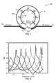
- FIG. 1 illustrates an example embodiment 10 of a distributedly modulated capacitor (DMC) based tunable notch filter of this disclosure comprising a ring resonator 12 which has a fixed resonant frequency coupled with the ring coupled to both input 14 and output 16 .
- DMC distributedly modulated capacitor
- the input and output ( 14 , 16 ) can be coupled to the ring resonator 12 by any desired form of proximity coupling, such as a capacitive coupling, or a 90 degree coupler.
- Ring resonator 12 is shown with two lines 20 a , 20 b , between which are coupled a plurality of variable capacitors 22 .
- a high pass filter (HPF) 18 is used to break the ring for the original received frequency and to allow the resonance to build up only at the up-converted frequency.
- the ring resonance notches out a fixed up-converted frequency.
- the original received band will also be selected correspondingly, except that it is continuously tunable by changing the carrier frequency.
- the length of the ring is approximately a quarter wavelength at the lowest frequency of operation, which may allow the complete structure to be integrated on-chip in some applications.
- FIG. 2 depicts a simulated tunable bandpass response of the filter.
- Each curve corresponds to the magnitude of the signal that is received at input 14 and passed to output 16 in FIG. 1 as a function of frequency.
- the different sets of curves correspond to different carrier frequency selections. It is evident that with each different carrier frequency setting, a corresponding frequency in the received signal is selected and the information at that frequency is passed and amplified, while the rest of the frequency is suppressed.
- DMCs which are a form of time-varying transmission line (TVTL) with finite length and periodical loading of varactor devices.
- TVTL time-varying transmission line
- varactor devices exemplified herein as varactor diodes which utilize a p-n junction in reverse bias, such that the capacitance of the diode varies with the reverse voltage.
- the operating principles of the DMCs were based on: (1) the distributed parametric effect on a time-varying transmission line; and (2) the distributed capacitive mixers.
- the theoretical bounds of the isolation and insertion performance of DMCs, as well as their noise performance, were also derived and served as guidance to practical implementations. Simulations were carried out and a prototype implemented which consisted of a double-balanced loading of varactor diodes on microstrip lines fabricated on low-loss dielectric printed circuit materials (i.e., Roger's board). The measured results were in close agreement with the theoretical derivations and the simulation results. This preliminary work is summarized as follows.
- FIG. 3 illustrates a lump-element circuit model 30 for a lossless infinite transmission line with time-varying capacitance.
- this transmission line 30 series inductors 32 a , 32 b , . . . , 32 n are seen interspersed with variable shunt capacitors 34 a , 34 b , 34 c , . . . , 34 n connected between the two lines of the transmission line.
- the Telegrapher's equations are modified to include the time variation of the capacitance per unit length:
- C ′ ⁇ ( z , t ) C 0 ′ + C m ′ ⁇ cos ⁇ ( ⁇ m ⁇ t - B m ⁇ z + ⁇ m ) ⁇ ⁇
- ⁇ ⁇ ⁇ m ⁇ m 1 LC 0 ( 3 )
- C′ 0 is the mean capacitance per unit length
- C′ m is the amplitude of the capacitance variation per unit length
- the carrier wave does not carry information. It is assumed that the carrier behaves as a pump signal with uniform amplitude along the transmission line, which drives the time-variation of the transmission line capacitance in a traveling wave fashion.
- a signal wave is launched into the same transmission line propagating toward the +z direction at the angular frequency ⁇ s .
- the signal is mixed up and down with the capacitance modulation signal at the angular frequency ⁇ m .
- the modulation frequency is normally chosen to be greater than the signal frequency ( ⁇ m > ⁇ s )
- the variation of the capacitance is small and the transmission line is non-dispersive over the bandwidth interested:
- v ⁇ ( z , t ) V s ⁇ ( z ) ⁇ cos ⁇ ( ⁇ s ⁇ t - ⁇ s ⁇ z + ⁇ s ) + V m - s ⁇ ( z ) ⁇ sin ⁇ ( ⁇ m - s ⁇ t - ⁇ m - s ⁇ z + ⁇ m - ⁇ s ) + V m + s ⁇ ( z ) ⁇ sin ⁇ ( ⁇ m + s ⁇ t - ⁇ m + s ⁇ z + ⁇ m + ⁇ s ) . ( 5 ⁇ - ⁇ 1 )
- the amplitudes at the three tones in Eq. (5-1) are functions of the propagation distance expressed as the following:
- V s ⁇ ( z ) V 0 ⁇ cos ⁇ ( 1 2 ⁇ 2 ⁇ ⁇ s ⁇ z ) , ( 5 ⁇ - ⁇ 2 )
- V m - s ⁇ ( z ) - V 0 2 ⁇ ⁇ m - s ⁇ s ⁇ sin ⁇ ( 1 2 ⁇ 2 ⁇ ⁇ s ⁇ z ) , ( 5 ⁇ - ⁇ 3 )
- V m + s ⁇ ( z ) - V 0 2 ⁇ ⁇ m + s ⁇ s ⁇ sin ⁇ ( 1 2 ⁇ 2 ⁇ ⁇ s ⁇ z ) , ( 5 ⁇ - ⁇ 4 )
- the non-reciprocal components promise low loss and low noise characteristics as the structure only consists of reactance based components, as opposed to active (transistor-based) components, or micro-electro-mechanical (MEMS) components.
- the waves at the up-converted frequencies can reach to the same or greater magnitude than that of the original signal wave, which occurs when a high carrier to signal dictated by the traveling directions of the signal and the carrier waves.
- the dispersion of DMC can be utilized to suppress some frequencies, by designing the stop bands at those frequencies as it will be seen in the described work.
- FIG. 4 illustrates an example embodiment 50 of a DMC connected to an antenna 68 on its right-hand side and a transceiver 52 on its left-hand side.
- a carrier is injected from the right-hand side of the DMC.
- the DMC is shown with a transceiver 52 having a transmitter (TX) 54 and receiver (RX) 56 .
- a combination transmit-receive line (TRL) 58 is shown for transmitting and receiving in opposite directions, with a line 60 for a carrier traveling in a single direction.
- Line 60 is shown with a carrier 64 coupled at a first end and a termination 66 coupled at a second end.
- a plurality of variable capacitances 62 a , 62 b , through to 62 i , and on through to 62 n - 1 and 62 n (which are varied as N, N ⁇ 1, through to i, and on through 2 and 1) are coupled between the transmission line 58 and ground.
- the capacitance of each capacitor is shown being varied in response to the carrier signal on line 60 .
- impedance exists ( ⁇ z)) between each capacitor along the transmission line, as denoted in the figure.
- the antenna 68 transmits and receives signals at the same frequency.
- the signal received by antenna 68 travels toward the transceiver 52 , and this signal is up-converted by the carrier upon its arrival at the transceiver because it travels in the same direction as the carrier.
- the transmitted signal does not mix with the carrier. It remains at its original frequency all the way to the antenna. Therefore, the transmitted signal and the received signal are at different frequencies at the transceiver end of the DMC, and with a frequency diplexer they can now be separated into a transmitter port and a receiver port. This separation is seen in the spectra shown in the figure.
- the transmission is seen 70 leaving TX 54 , which arrives with spectrum 72 at the antenna end of the transmission line.
- a signal 74 (showing a single component) is received at the receiver, with the spectrum 76 (showing three signal components) reaching RX 56 .
- the carrier 78 is shown conveyed on line 60 .
- the device illustrated in FIG. 4 plays the role of a circulator if the receiver operating frequency is modified accordingly.
- the device up shifts the signal frequency if it entered from the antenna and keeps the frequency the same if it enters from the transmitter.
- the up-shifted received signal is thus routed to the RX port 56 by the diplexer while the transmit signal entered 54 will propagates through to the antenna.
- noise figure formula for the embodiment of FIG. 4 can thus be derived as
- NF ( dB ) 10 ⁇ log 10 ⁇ ( 1 + 1 3 ⁇ ⁇ s ⁇ z Q s + 16 ⁇ 2 ⁇ ⁇ 1 Q m ⁇ s ⁇ ⁇ m ⁇ s ⁇ z ) , ( 6 ) where Q s and Q m ⁇ s are quality factors of the loaded transmission line respectively at the original received frequency and the up-converted frequencies, which are estimated as
- FIG. 5A and FIG. 5B illustrate DMCs implemented in double balanced fashion.
- a transmission line 90 is realized with two units shown in a three dimensional configuration, with carrier lines C+ 92 a , C ⁇ 92 b , signal lines S+ 94 a , and S ⁇ 94 b , and varactor diodes 96 interconnecting between each of the signal lines for each unit cell along these lines.
- the cathode sides of the varactor diodes are oriented toward C+ 92 a and S+ 94 a respectively.
- the double balanced configuration as depicted allows the cancellation of the capacitance modulation caused by the signal voltage and the construction of the capacitance modulation caused by the carrier voltage. This is to achieve the transmission line capacitance modulation solely by the carrier while maintaining the linearity of the signal in transmitting and receiving.
- a microstrip line implementation 130 is depicted with one unit shown.
- this substrate comprises a microstrip line realization (shown here in cross-section).
- C+ 92 a , and C ⁇ 92 b lines are duplicated on each side of lines S+ 94 a , and S ⁇ 94 b which are interconnected between each unit cell with varactor diodes 96 , as was seen in FIG. 1 .
- Bonding wires 136 , 138 are seen interconnecting the two C+ lines 92 a , and the two C ⁇ lines 92 b .
- the S lines could be duplicated and placed on each side of the C lines.
- FIG. 6 illustrates (as a rendition of a photographic image) an embodiment 190 of the microstrip implementation developed on a low-loss dielectric printed circuit board (i.e., Rogers board).
- a low-loss dielectric printed circuit board i.e., Rogers board.
- the signal lines S+ 192 a , S ⁇ 192 b , and carrier line C+ 194 a , C ⁇ 194 b This example comprises 16 unit cells, each of which contain the four varactor diodes, (as seen in FIG. 1 ).
- Structures 197 a and 197 b at each end of the lines are cross-overs of the transmission lines, the position of which is merely indicated with the dashed line circles to allow seeing the underlying traces.
- FIG. 7 is a plot of measured insertion loss and the isolation compared against the theory values. It can be seen the measured performance has a high level of agreement with the corresponding theoretical values.
- the nonlinear terms such as the self-modulation of the signal waves are mostly cancelled with the balanced architecture except the first order modulation term between the signal and the carrier wave.
- the IP3 of the TVTL with commercial devices can reach a few watts and it can be further improved with high breakdown voltage devices.
- the TVTL can be considered as a linear network whose transfer relationship is only determined by the level and the frequency of the carrier modulation. This is similar to the case when large signal approximation is applied to the mixer analysis. Such a network can thus serve as a fundamental building block for circuit design with more functionality.
- the disclosure here will be primarily focused on the novel features resulted when feedbacks and resonances are introduced in the structures.
- a gain enhancement effect over a narrow bandwidth is expected, which may help to reduce the length of the structure and the power consumption on the carrier while increasing the frequency selectivity.
- the outgoing waves from the structure at the original signal ⁇ s , the lower sideband of the up-converted signal ⁇ m ⁇ s and the upper sideband of the up-converted signal ⁇ m+s are given by Eq. (5). They can be expressed in complex phasors as follows,
- V ⁇ m - s * - ⁇ ( z ) - j ⁇ 1 2 ⁇ ⁇ m - s ⁇ s ⁇ sin ⁇ ⁇ ( 1 2 ⁇ 2 ⁇ ⁇ s ⁇ z ) ⁇ e j ⁇ ⁇ ⁇ m - s ⁇ z ⁇ e j ⁇ ⁇ ⁇ m ⁇ V ⁇ s + ⁇
- V ⁇ s - ⁇ ( z ) j ⁇ 1 2 ⁇ ⁇ s ⁇ m - s ⁇ sin ⁇ ⁇ ( 1 2 ⁇ 2 ⁇ ⁇ m - s ⁇ z ) ⁇ e - j ⁇ ⁇ ⁇ s ⁇ z ⁇ e j ⁇ ⁇ ⁇ m ⁇ V ⁇ m - s * + ⁇ ( 0 )
- V ⁇ m - s * - ⁇ ( z ) cos ⁇ ⁇ ( 1 2 ⁇ 2 ⁇ ⁇ m - s ⁇ z ) ⁇ e j ⁇ ⁇ ⁇ m - s ⁇ z ⁇ V ⁇ m - s * + ⁇ ( 0 ) . ( 9 )
- [ T 1 ] [ cos ⁇ ⁇ ( 1 2 ⁇ 2 ⁇ ⁇ s ⁇ z ) ⁇ e - j ⁇ ⁇ ⁇ s ⁇ z j ⁇ 1 2 ⁇ ⁇ s ⁇ m - s ⁇ sin ⁇ ⁇ ( 1 2 ⁇ 2 ⁇ ⁇ m - s ⁇ z ) ⁇ e - j ⁇ ⁇ ⁇ s ⁇ z ⁇ e j ⁇ ⁇ ⁇ m - j ⁇ 1 2 ⁇ ⁇ m - s ⁇ s ⁇ sin ⁇ ⁇ ( 1 2 ⁇ 2 ⁇ ⁇ s ⁇ ) ⁇ e j ⁇ ⁇ ⁇ m - s ⁇ z ⁇ e j ⁇ ⁇ ⁇ m cos ⁇ ⁇ ( 1 2 ⁇ 2 ⁇ ⁇ m - s ⁇ z ) ⁇ e j ⁇ ⁇ ⁇
- FIG. 8 illustrates 210 a convenient means of representing the non-reciprocal coupling across different frequencies at different ports 214 , 216 of the TVTL 212 .
- the TVTL implemented in the form of DMC is a periodic structure with cut-off frequencies.
- a particularly interesting case is when the cut-off frequency is placed beyond the first two tones, say, ⁇ m+s and above.
- the Bloch impedance beyond the cut-off approaches to short circuit so that the voltages on TVTL at those frequencies are forced to be zero.
- a matrix similar to Eq. (10) can be derived,
- FIG. 9 illustrates an embodiment 230 of DMC in which an antenna 232 is coupled at a first portion 233 of a first port of TVTL 212 , with output from a first portion 240 of a second port to a transceiver 242 having transmitter 244 a , and receiver 244 b , from which are seen a connection 246 to a transmitter, and 248 to a receiver.
- the second portions 234 , 238 of the first and second ports are seen coupled 236 in a feedback arrangement.
- the feedback allows a resonance to build up at ⁇ m ⁇ s when the denominator 1 ⁇ t 22 approaches zero. This forms a sharply rising gain around the resonant frequency.
- the objective of the design is to couple this strong frequency selectivity at ⁇ m ⁇ s to the original RF signal domain at ⁇ s through the control of the modulation carrier frequency at ⁇ m .
- the resonant frequency coupled to the original RF signal domain is tunable by changing the modulation carrier frequency without the need of modifying the physical resonance of the resonator at ⁇ m ⁇ s . Therefore it will be appreciated that the present disclosure can provide a wide range of frequency tuning.
- a notch amplifier such as this could be applied in a number of beneficial ways, for example by being inserted before the diplexer of a wireless front-end to boost up the received signal power and suppress the blocker interference from adjacent channels.
- This form of notch amplifier also helps to relieve the diplexer requirement, as the received signal power versus the transmitter leakage into the receiver is effectively increased by the gain of the notch amplifier. To quantitatively analyze the frequency dependency in gain, it yields,
- G ss ⁇ ( z ) [ cosh ⁇ ⁇ ( 1 4 ⁇ ⁇ 1 ⁇ ⁇ s ⁇ ⁇ m - s ⁇ z ) + sinh 2 ⁇ ( 1 4 ⁇ ⁇ ⁇ ⁇ s ⁇ ⁇ m - s ⁇ z ) ⁇ e j ⁇ ⁇ ⁇ m - s ⁇ z 1 - cosh ⁇ ( 1 4 ⁇ ⁇ ⁇ s ⁇ ⁇ m - s ⁇ z ⁇ e j ⁇ ⁇ ⁇ m - s ⁇ z ] ⁇ e - j ⁇ ⁇ ⁇ s ⁇ z ] ⁇ e - j ⁇ ⁇ ⁇ s ⁇ z . ( 16 )
- G ss ⁇ ( z ) [ cosh ⁇ ⁇ ( 1 4 ⁇ ⁇ 1 ⁇ ⁇ s ⁇ ⁇ m - s ) + sinh 2 ⁇ ( 1 4 ⁇ ⁇ ⁇ ⁇ s ⁇ ⁇ m - s ⁇ z ) ⁇ e - ⁇ m - s ⁇ z 1 - cosh ⁇ ( 1 4 ⁇ ⁇ ⁇ ⁇ s ⁇ ⁇ - s ⁇ z ) e - ⁇ m - s ⁇ z ⁇ e - ⁇ m - s ⁇ z ⁇ e ⁇ j ⁇ ⁇ ⁇ m - s ⁇ z ] ⁇ e - ( ⁇ s + j ⁇ ⁇ ⁇ s ) ⁇ z ( 17 )
- ⁇ m ⁇ s is the deviation of ⁇ m ⁇ s from the resonance condition ⁇ m ⁇ s
- the enhanced quality factor Q E is generally greater than the quality factor of the passive ring resonator Q m ⁇ s , as it is parametrically enhanced with the energy from the carrier supplied into the system through the TVTL.
- FIG. 10 illustrates an example embodiment 250 of the non-reciprocal tunable notch amplifier whose conceptually was depicted in FIG. 9 .
- the TVTL is realized with a pair of transmission lines 270 a , 270 b , loaded with oppositely loaded varactors diodes 272 a , 272 b .
- the original RF signal is received at input 252 through a parallel LC (inductor 256 a with parallel capacitor 256 b ), and the modulation carrier 264 are fed to the pair of the transmission lines through a 180 degree hybrid 262 , so that the original RF signal drives the lines in a common mode while the modulation carrier drives the line in a difference mode.
- the self-modulation terms e.g., the capacitance variation caused by the signal voltage
- the carrier modulation to the transmission line capacitance are enhanced, after both of them arrive at the second 180-degree hybrid 266 , shown with termination 268 .
- the design of the tunable notch amplifier starts by selecting a fixed ⁇ m ⁇ s .
- the RF output at the end of the resonator passes through another parallel LC (inductor 260 a with parallel capacitor 260 b ).
- a series LC resonator having inductor 258 a in series with capacitor 258 b , at this pre-selected frequency is placed between the beginning and the end of the TVTL, passing ⁇ m ⁇ s and rejecting all the other frequencies so that the resonance can only be formed at this single frequency.
- the RF input and output are tapped into the ring resonator each through a ⁇ m ⁇ s rejecting filter so the energy of the resonance at ⁇ m ⁇ s is isolated from the source and the load of the RF signal.
- each line in the TVTL was loaded with 16 varactor diodes with the total length being approximately one wavelength at 2.67 GHz.
- each diode has a mean capacitance of 0.11 pF with a variation of +/ ⁇ 0.03 pF under the given modulation, and a series resistance of 1.8 Ohm ( ⁇ ) according to the standard specs of 0.1 ⁇ m GaN HEMT varactor diode technology.
- the resonance frequency is selected to 7 GHz, which corresponds to the third resonance mode of the ring structure.
- the modulation carrier frequency is from 7.8 GHz to 9.6 GHz, which corresponds to the input RF frequency of 800 MHz to 2.6 GHz.
- the carrier power used to drive the TVTL is 19 dBm.
- FIG. 11A and FIG. 11B depict plots of simulated gain and noise figure over the tunable notches, respectively.
- the results show good agreement (matching) with the theory, with demonstration of extremely sharp notches with RF amplifications tunable from 800 MHz to 2.6 GHz.
- the maximum gain is approximately 15 dB at the 2.6 GHz center frequency, with a 3 dB bandwidth of merely 10 MHz. It corresponds to a system Q of 260 while the intrinsic Q of the resonator is only about 100. This has demonstrated that the system Q is indeed enhanced with the parametric effect.
- the noise figures are generally low from 0.4 dB to a maximum of 1.1 dB, which are comparable to the noise performance of the state of the art transistor based low noise amplifiers.
- FIG. 12A illustrates another example embodiment 290 with a similar device architecture configured to channel the received signal from the lower sideband of the up-converted signal, e.g., at ⁇ m ⁇ s through an input 293 of the device.
- a first port is seen with antenna 292 coupled to a first connection 293 , and a feedback path 296 coupled between a second connection 294 , and a second connection 300 of a second port.
- the original RF output 302 is now for the transmitting path only (to transmitter), and an output to the receiver 298 seen coupled in the feedback path.
- the coupling can be achieved with a capacitive coupling, inductive coupling or any other proximity coupling approach.
- the receiving transfer function of such a device is G m ⁇ s,s as described in Eq. (15).
- the transmitting and receiving are separated to different frequencies that are far apart (separated at significantly different frequencies) from each other after they pass through this device, a sharp diplexer is no longer needed. It can be used as a circulator providing full duplex capabilities much like the original TVTL without feedback.
- the receiving path of this device behaves effectively like a tunable filter offering superior suppression to the out of band signals, as the changing of the modulation carrier frequency effectively selects the RF frequency band to be up-converted and amplified to ⁇ m ⁇ s .
- a similar structure like the previous one is simulated in ADS, except in this case a 15 dB coupler is inserted to couple the resonance signal from the ring out to a load.
- FIG. 12B illustrates an example embodiment 310 of a non-reciprocal tunable notch amplifier having the receiver coupling configuration represented in FIG. 12A .
- the TVTL has a pair of transmission lines 332 a , 332 b , loaded with oppositely loaded varactors diodes 334 a , 334 b .
- the original RF signal is received at input 312 through a parallel LC (inductor 318 a with parallel capacitor 318 b ), and the modulation carrier 326 are fed to the pair of the transmission lines through a 180 degree hybrid 324 .
- a second 180-degree hybrid 328 is shown with termination 330 .
- a transmitter input 316 is shown passing through another parallel LC (inductor 320 a with parallel capacitor 320 b ) to the sum input of hybrid 328 .
- a series LC resonator, having inductor 322 a in series with capacitor 322 b are coupled between the beginning and the end of the TVTL.
- Receiver output 318 is shown with proximity coupling to the series LC resonator ( 322 a , 322 b ) to provide for the receiver output RX@ ⁇ m ⁇ s 314 .
- Tunable notches with a moderate amount of gain ranging from 4 to 7 dB were achieved over the frequency tuning range of 800 MHz to 2.4 GHz.
- the system Q is slightly reduced from the previous case due to coupling of the resonance energy to the load.
- out of band suppression is significantly better, mostly in the level of 25 to 30 dB, which is quite good as the fundamental resonant frequency of the ring resonator is 2.67 GHz, which is much higher than the operating frequency here.
- DMC Distributedly Modulated Capacitor
- DMC Distributedly Modulated Capacitors
- DMC Distributedly Modulated Capacitors
- the disclosed implementations of Distributedly Modulated Capacitors (DMC) have created a new paradigm for devices operating over a broad band, with low noise, at high power while providing frequency translation capability.
- the broadband feature and the frequency translation function of DMC can be utilized to develop a front-end with tunable notch filtering capability.
- the DMC behaves like a mixer with almost no noise or extremely low noise, it can be used to shift the whole received band in the frequency domain and so the signal through a fixed notch filter can be filtered at the designated frequency.
- FIG. 13 illustrates an example embodiment 350 of such a broadband, frequency translation DMC front-end.
- an antenna 352 and carrier 354 are shown coupled to a first port of the DMC chip 356 , such as implementation of the DMC illustrated in FIG. 8 in either an on-chip form or on a printed circuit board.
- Output 358 of the DMC is connected to a transceiver 360 having a transmitter (TX) 362 a , and receiver (RX) 362 b .
- TX transmitter
- RX receiver
- Signals are seen received by TX 362 a through a multiple-band power amplifier (PA) 364 , depicted by way of example with amplifiers 366 a , 366 b .
- PA multiple-band power amplifier
- signals are seen output from RX 362 b through a single-band low-noise amplifier (LNA) 368 .
- LNA low-noise amplifier
- a fixed RX filter from DMC 356 is used in conjunction with a tunable carrier input at DMC, and converts the desired received signal into the pass band of the filter while leaving the blocker signal outside the pass band.
- FIG. 14A through FIG. 14C illustrates the sequence of separation of this signal from that of FIG. 13 .
- the received signal is seen at the antenna in FIG. 14A , at the output of the DMC in FIG. 14B , and at the output of the RX filter in FIG. 14C .
- certain advantages are gained in the system front-end of FIG. 13 by integrating the design of the DMC with the fixed filter.
- the DMC can be included as part of the filter and it can be designed to have a small amount of positive gain to compensate the possible insertion loss.
- An example of such designs was shown in FIG. 1 , where DMC is integrated as part of a ring resonator.
- the dimension of the ring structure supports resonances at a fixed up-converted signal frequency while it suppresses the possible resonance at the original signal frequency by breaking the loop apart with a high pass filter.
- the selection and filtering of the original signal frequency can thus be performed by varying the carrier frequency.
- the DMC transmission line structure is designed with a moderate loop gain to achieve high quality factor in its frequency selection.
- a 6 GHz ring resonator is designed, which allows the tuning of the notch filtering at the frequency of 400 MHz to 1 GHz.
- the simulated results showed highly selective bandpass characteristics with a loaded quality factor in a range of 100 to 200, yet it can be tuned continuously for more than one octave by varying the carrier frequency. It should be noted that the insertion gain is slightly positive for some frequencies due to the parametric amplification effects of the DMC.
- the present disclosure encompasses multiple embodiments which include, but are not limited to: (a) a distributedly modulated capacitor (DMC) tunable notch filter, (b) a distributedly modulated capacitor (DMC) circulator, and (c) a tunable notch filter comprising a distributedly modulated capacitor (DMC) integrated into a ring resonator.
- DMC distributedly modulated capacitor
- DMC distributedly modulated capacitor
- DMC distributedly modulated capacitor
- a distributedly modulated capacitor (DMC) tunable notch filter apparatus comprising: a ring resonator comprising distributedly modulated capacitors (DMC) in a ring structure comprising at least one transmission line; a high pass filter (HPF) interposed within said ring resonator to allow resonance to build up only at an up-converted frequency; a receiver input and carrier signal coupled to said ring resonator which is coupled to a receiver output; wherein said transmission line has a direction dependency for propagating carrier waves in a first direction, and propagating signal waves in a second direction; wherein said distributedly modulated capacitors (DMC) comprise a plurality of time-varying capacitance elements configured for shunt capacitance modulation in response to carrier wave frequency; and wherein said ring resonator notches out a fixed up-converted frequency, providing continuous tunability of a received band in response to changing the carrier frequency, so that it frequency tunes an entire received band instead of a resonant frequency of the high-pass filter (
- any preceding embodiment further comprising: a first 180 degree hybrid and a second 180 degree hybrid within said high pass filter; wherein said receiver input is fed to a sum input of said first 180 degree hybrid with said carrier signal fed to a difference input on said first 180 degree hybrid; and wherein said receiver output is generated from a sum output on said second 180 degree hybrid.
- any preceding embodiment further comprising: a first 180 degree hybrid and a second 180 degree hybrid within said high pass filter; wherein said receiver input is fed to a sum input of said first 180 degree hybrid with said carrier signal fed to a difference input on said first 180 degree hybrid; wherein a transmitter input is coupled to a sum output on said second 180 degree hybrid; and a series LC resonator is coupled between sum outputs of said first and second 180 degree hybrids; wherein said receiver output is coupled to the inductor in said LC resonator.
- time-varying capacitance elements comprise varactor diodes.
- DMC distributedly modulated capacitor
- a distributedly modulated capacitor (DMC) circulator apparatus comprising: at least one transmission line having distributedly modulated capacitors (DMC) coupled to its conductors; an antenna configured for transmitting signals at a given frequency from a transmitter, and receiving signals at that same given frequency directed towards a receiver; wherein said antenna is coupled to a first side of a first conductor of said at least one transmission line; a carrier signal coupled to a first side of a second conductor of said at least one transmission line; wherein said distributedly modulated capacitors (DMC) comprise a plurality of time-varying capacitance elements configured for shunt capacitance modulation in response to receipt of said carrier signal; a transceiver, having a transmitter and receiver, coupled to a second side of a first conductor of said at least one transmission line; wherein said at least one transmission line is configured for propagating carrier and receiver signal waves from an antenna in a first direction on said at least one transmission line, while at least one transmitter signal is propagated in a second direction, opposite of said first direction,
- time-varying capacitance elements comprise varactor diodes.
- a distributedly modulated capacitor (DMC) tunable notch filter apparatus comprising: at least one transmission line having distributedly modulated capacitors (DMC) coupled to its conductors; wherein said at least one transmission line is configured for propagating a receiver signal and a carrier signal in a first direction from a first end of said at least one transmission through said at least one transmission line which up-converts said receiver signal, into an up-converted receiver signal, by said carrier signal because it travels in an identical direction as said carrier signal; wherein said distributedly modulated capacitors (DMC) comprise a plurality of time-varying capacitance elements configured for shunt capacitance modulation in response to receipt of said carrier signal; and a fixed bandpass filter or diplexer coupled to a second end of said at least one transmission line, wherein said fixed bandpass filter or diplexer selects a frequency of said up-converted receiver signal as a receiver output.
- DMC distributedly modulated capacitor
- time-varying capacitance elements comprise varactor diodes.
Landscapes
- Transmitters (AREA)
- Transceivers (AREA)
Abstract
Description
where L′ and C′ are inductance and capacitance per unit length, respectively. Rearranging the equations in Eq. (1-1 and 1-2) yields
where C′0 is the mean capacitance per unit length, C′m is the amplitude of the capacitance variation per unit length, βm is the phase constant of the carrier with a phase velocity of vp=ωm/βm=1/√{square root over (L′C′0)}. The carrier wave does not carry information. It is assumed that the carrier behaves as a pump signal with uniform amplitude along the transmission line, which drives the time-variation of the transmission line capacitance in a traveling wave fashion.
where
ξ=C′ m /C′ 0 (5-5)
is defined as the capacitance modulation index.
where Qs and Qm±s are quality factors of the loaded transmission line respectively at the original received frequency and the up-converted frequencies, which are estimated as
where Qd,s and Qd,m±s are respectively the quality factors of the varactor diodes at the original received frequency and the up-converted frequencies. From Eq. (6), one can see that the second type of noise dominates, until the structure is significantly longer than the wavelength so that the power of the first type of noise will rise to be comparable. It is also evident from Eq. (6) that varactors with high quality factors and high capacitance modulation indices will result in a low noise DMC.
where the superscripts “+” and “−” represent incoming and outgoing waves respectively similar to that in the definition of scattering parameters. It is evident from Eq. (8) that the amplitude and phase of the outgoing waves at all the three tones are linearly proportional to that of the incoming wave at the original signal frequency. Alternatively, the outgoing waves out of the network in the case that the incidence is only at the tone ωm−s are yielded as,
It shows the coupling across the different frequencies is determined by the propagating distance and the modulation level. On the other hand, such coupling disappears when the incidence is opposite to the propagating direction of the carrier wave, yielding
{tilde over (V)}* m−s −(z)=t 21 {tilde over (V)} s(0)+t 22 {tilde over (V)}* m−s +(0)=t 21 {tilde over (V)} s(0)+t 22 {tilde over (V)}* m−s −(z) (14)
which leads to the following relationship,
where Gss is the voltage gain at the original signal frequency and Gm−s,s is the cross frequency voltage gain between the output voltage at ωm−s and the input voltage at ωs. It is clear from the above that the feedback allows a resonance to build up at ωm−s when the
where Δβm−s is the deviation of βm−s from the resonance condition βm−sz=2π. Define λ=1/4ξ√{square root over (βsβm−s)}, for small resonators, λz is generally much smaller than one, so Taylor expansions with small variable approximation can be applied to simplify the expression,
where Qp is the parametric quality factor determined by the modulation index and the electrical length of the ring resonator operating frequency. It is defined by
Claims (24)
Priority Applications (1)
| Application Number | Priority Date | Filing Date | Title |
|---|---|---|---|
| US14/956,036 US10027306B2 (en) | 2014-12-02 | 2015-12-01 | Non-reciprocal, tunable notch amplifying RF front-ends based on distributedly modulated capacitors (DMC) |
Applications Claiming Priority (2)
| Application Number | Priority Date | Filing Date | Title |
|---|---|---|---|
| US201462086545P | 2014-12-02 | 2014-12-02 | |
| US14/956,036 US10027306B2 (en) | 2014-12-02 | 2015-12-01 | Non-reciprocal, tunable notch amplifying RF front-ends based on distributedly modulated capacitors (DMC) |
Publications (2)
| Publication Number | Publication Date |
|---|---|
| US20160156327A1 US20160156327A1 (en) | 2016-06-02 |
| US10027306B2 true US10027306B2 (en) | 2018-07-17 |
Family
ID=56079835
Family Applications (1)
| Application Number | Title | Priority Date | Filing Date |
|---|---|---|---|
| US14/956,036 Active 2036-04-19 US10027306B2 (en) | 2014-12-02 | 2015-12-01 | Non-reciprocal, tunable notch amplifying RF front-ends based on distributedly modulated capacitors (DMC) |
Country Status (1)
| Country | Link |
|---|---|
| US (1) | US10027306B2 (en) |
Families Citing this family (12)
| Publication number | Priority date | Publication date | Assignee | Title |
|---|---|---|---|---|
| US9396368B1 (en) | 2015-05-23 | 2016-07-19 | Square, Inc. | Tuning a NFC antenna of a device |
| US11410154B2 (en) | 2015-06-05 | 2022-08-09 | Block, Inc. | Apparatuses, methods, and systems for transmitting payment proxy information |
| US10482440B1 (en) | 2015-09-18 | 2019-11-19 | Square, Inc. | Simulating NFC experience |
| US10861003B1 (en) | 2015-09-24 | 2020-12-08 | Square, Inc. | Near field communication device coupling system |
| US10198727B1 (en) * | 2015-09-25 | 2019-02-05 | Square, Inc. | Modulation of a near-field communication signal |
| US10008982B1 (en) * | 2016-02-19 | 2018-06-26 | Rockwell Collins, Inc. | Parametrically driven gyromagnetic nonlinear transmission line oscillator |
| US10430784B1 (en) | 2017-08-31 | 2019-10-01 | Square, Inc. | Multi-layer antenna |
| CN108337010B (en) * | 2018-01-03 | 2020-02-18 | 浙江大学 | A Radio Frequency Receiver Based on Carrier Enhancement Technology |
| US11182770B1 (en) | 2018-12-12 | 2021-11-23 | Square, Inc. | Systems and methods for sensing locations of near field communication devices |
| US10608613B1 (en) * | 2019-06-07 | 2020-03-31 | Northrop Grumman Systems Corporation | Non-reciprocal band pass filter |
| CN119994423B (en) * | 2025-04-17 | 2025-07-08 | 中天通信技术有限公司 | Tunable cavity filter coupler, antenna device and communication equipment |
| CN121217090A (en) * | 2025-09-22 | 2025-12-26 | 成都兴仁科技有限公司 | A radio frequency control method based on tuning response and harmonic optimization |
-
2015
- 2015-12-01 US US14/956,036 patent/US10027306B2/en active Active
Also Published As
| Publication number | Publication date |
|---|---|
| US20160156327A1 (en) | 2016-06-02 |
Similar Documents
| Publication | Publication Date | Title |
|---|---|---|
| US10027306B2 (en) | Non-reciprocal, tunable notch amplifying RF front-ends based on distributedly modulated capacitors (DMC) | |
| US6803835B2 (en) | Integrated filter balun | |
| US9449749B2 (en) | Signal handling apparatus for radio frequency circuits | |
| US9577847B2 (en) | Non-reciprocal components with balanced distributedly modulated capacitors (DMC) | |
| US9438288B2 (en) | System providing reduced intermodulation distortion | |
| US7983627B2 (en) | Circuit arrangement with improved decoupling | |
| US10116281B2 (en) | Power combiner/divider using mutual inductance | |
| Qin et al. | Broadband parametric circulator with balanced monolithic integrated distributedly modulated capacitors (DMC) | |
| US9413050B2 (en) | Distributedly modulated capacitors for non-reciprocal components | |
| JP3851900B2 (en) | Planar filter, semiconductor device, and wireless device | |
| US20220278434A1 (en) | Duplexers and related devices for 5g/6g and subsequent protocols and for mm-wave and terahertz applications | |
| Keshavarz et al. | A quad-band distributed amplifier with E-CRLH transmission line | |
| Wang | Time-varying transmission lines (TVTL)-A new pathway to non-reciprocal and intelligent RF front-ends | |
| Keshavarz et al. | Compact active duplexer based on CSRR and interdigital loaded microstrip coupled lines for LTE application | |
| EP3055946B1 (en) | Signal processing device, amplifier, and method | |
| JPH10256809A (en) | Electronically tuned polarized filter | |
| KR100730491B1 (en) | Electronic circuit device | |
| KR100991145B1 (en) | Compact Ring Hybrid with Broadband Characteristics Using Meta-materials and Parallel Capacitors | |
| Güner | Ka-band full duplex system with electrical balance duplexer for 5G applications using SiGe BiCMOS technology | |
| Borah | Differential multiband reconfigurable filters for RF front-end applications | |
| US20250300347A1 (en) | Phase shift circuit, antenna system, and communication device | |
| Simpson | Reconfigurable RF Filters and Wideband Constant-HPBW Antenna Arrays for Next-Generation Radios | |
| Abdaoui et al. | Microstrip band pass filter bank for 60 GHz UWB impulse radio multi band architectures | |
| Nagulu | Surpassing Fundamental Limits Through Time Varying Electromagnetics | |
| KR20040015543A (en) | Structure for balun |
Legal Events
| Date | Code | Title | Description |
|---|---|---|---|
| AS | Assignment |
Owner name: THE REGENTS OF THE UNIVERSITY OF CALIFORNIA, CALIF Free format text: ASSIGNMENT OF ASSIGNORS INTEREST;ASSIGNOR:WANG, YUANXUN ETHAN;REEL/FRAME:037600/0525 Effective date: 20151201 |
|
| STCF | Information on status: patent grant |
Free format text: PATENTED CASE |
|
| MAFP | Maintenance fee payment |
Free format text: PAYMENT OF MAINTENANCE FEE, 4TH YR, SMALL ENTITY (ORIGINAL EVENT CODE: M2551); ENTITY STATUS OF PATENT OWNER: SMALL ENTITY Year of fee payment: 4 |
|
| MAFP | Maintenance fee payment |
Free format text: PAYMENT OF MAINTENANCE FEE, 8TH YR, SMALL ENTITY (ORIGINAL EVENT CODE: M2552); ENTITY STATUS OF PATENT OWNER: SMALL ENTITY Year of fee payment: 8 |