US10026826B2 - Method of forming semiconductor device having gate dielectric surrounding at least some of channel region and gate electrode surrounding at least some of gate dielectric - Google Patents
Method of forming semiconductor device having gate dielectric surrounding at least some of channel region and gate electrode surrounding at least some of gate dielectric Download PDFInfo
- Publication number
- US10026826B2 US10026826B2 US15/338,667 US201615338667A US10026826B2 US 10026826 B2 US10026826 B2 US 10026826B2 US 201615338667 A US201615338667 A US 201615338667A US 10026826 B2 US10026826 B2 US 10026826B2
- Authority
- US
- United States
- Prior art keywords
- region
- forming
- dielectric
- type
- type region
- Prior art date
- Legal status (The legal status is an assumption and is not a legal conclusion. Google has not performed a legal analysis and makes no representation as to the accuracy of the status listed.)
- Active
Links
- 239000004065 semiconductor Substances 0.000 title claims abstract description 91
- 238000000034 method Methods 0.000 title claims description 44
- 239000000463 material Substances 0.000 claims description 78
- 239000002019 doping agent Substances 0.000 claims description 22
- 239000000758 substrate Substances 0.000 claims description 20
- 238000009792 diffusion process Methods 0.000 claims description 11
- 238000005530 etching Methods 0.000 claims description 11
- 239000000203 mixture Substances 0.000 claims description 7
- VYPSYNLAJGMNEJ-UHFFFAOYSA-N Silicium dioxide Chemical compound O=[Si]=O VYPSYNLAJGMNEJ-UHFFFAOYSA-N 0.000 description 11
- ZOXJGFHDIHLPTG-UHFFFAOYSA-N Boron Chemical compound [B] ZOXJGFHDIHLPTG-UHFFFAOYSA-N 0.000 description 9
- GYHNNYVSQQEPJS-UHFFFAOYSA-N Gallium Chemical compound [Ga] GYHNNYVSQQEPJS-UHFFFAOYSA-N 0.000 description 9
- 229910052787 antimony Inorganic materials 0.000 description 9
- WATWJIUSRGPENY-UHFFFAOYSA-N antimony atom Chemical compound [Sb] WATWJIUSRGPENY-UHFFFAOYSA-N 0.000 description 9
- 229910052785 arsenic Inorganic materials 0.000 description 9
- RQNWIZPPADIBDY-UHFFFAOYSA-N arsenic atom Chemical compound [As] RQNWIZPPADIBDY-UHFFFAOYSA-N 0.000 description 9
- 229910052796 boron Inorganic materials 0.000 description 9
- 229910052733 gallium Inorganic materials 0.000 description 9
- BHEPBYXIRTUNPN-UHFFFAOYSA-N hydridophosphorus(.) (triplet) Chemical compound [PH] BHEPBYXIRTUNPN-UHFFFAOYSA-N 0.000 description 9
- 229910052738 indium Inorganic materials 0.000 description 9
- APFVFJFRJDLVQX-UHFFFAOYSA-N indium atom Chemical compound [In] APFVFJFRJDLVQX-UHFFFAOYSA-N 0.000 description 9
- 238000005229 chemical vapour deposition Methods 0.000 description 8
- 238000000151 deposition Methods 0.000 description 7
- XUIMIQQOPSSXEZ-UHFFFAOYSA-N Silicon Chemical compound [Si] XUIMIQQOPSSXEZ-UHFFFAOYSA-N 0.000 description 6
- 230000008021 deposition Effects 0.000 description 6
- 229910021420 polycrystalline silicon Inorganic materials 0.000 description 6
- 229920005591 polysilicon Polymers 0.000 description 6
- 229910052710 silicon Inorganic materials 0.000 description 6
- 239000010703 silicon Substances 0.000 description 6
- -1 for example Substances 0.000 description 5
- 239000012212 insulator Substances 0.000 description 5
- 239000000377 silicon dioxide Substances 0.000 description 5
- 238000000231 atomic layer deposition Methods 0.000 description 4
- 229910052732 germanium Inorganic materials 0.000 description 4
- GNPVGFCGXDBREM-UHFFFAOYSA-N germanium atom Chemical compound [Ge] GNPVGFCGXDBREM-UHFFFAOYSA-N 0.000 description 4
- 229910052581 Si3N4 Inorganic materials 0.000 description 3
- 239000004020 conductor Substances 0.000 description 3
- 239000003989 dielectric material Substances 0.000 description 3
- 235000012239 silicon dioxide Nutrition 0.000 description 3
- HQVNEWCFYHHQES-UHFFFAOYSA-N silicon nitride Chemical compound N12[Si]34N5[Si]62N3[Si]51N64 HQVNEWCFYHHQES-UHFFFAOYSA-N 0.000 description 3
- 229910001218 Gallium arsenide Inorganic materials 0.000 description 2
- 229910000530 Gallium indium arsenide Inorganic materials 0.000 description 2
- 229910000673 Indium arsenide Inorganic materials 0.000 description 2
- 229910004166 TaN Inorganic materials 0.000 description 2
- ATJFFYVFTNAWJD-UHFFFAOYSA-N Tin Chemical compound [Sn] ATJFFYVFTNAWJD-UHFFFAOYSA-N 0.000 description 2
- 230000004075 alteration Effects 0.000 description 2
- 229910052782 aluminium Inorganic materials 0.000 description 2
- XAGFODPZIPBFFR-UHFFFAOYSA-N aluminium Chemical compound [Al] XAGFODPZIPBFFR-UHFFFAOYSA-N 0.000 description 2
- 230000008901 benefit Effects 0.000 description 2
- 230000015572 biosynthetic process Effects 0.000 description 2
- 229910052681 coesite Inorganic materials 0.000 description 2
- 229910052906 cristobalite Inorganic materials 0.000 description 2
- 238000000407 epitaxy Methods 0.000 description 2
- 230000006870 function Effects 0.000 description 2
- RPQDHPTXJYYUPQ-UHFFFAOYSA-N indium arsenide Chemical compound [In]#[As] RPQDHPTXJYYUPQ-UHFFFAOYSA-N 0.000 description 2
- 230000004048 modification Effects 0.000 description 2
- 238000012986 modification Methods 0.000 description 2
- 239000002070 nanowire Substances 0.000 description 2
- 238000005240 physical vapour deposition Methods 0.000 description 2
- 238000005498 polishing Methods 0.000 description 2
- 229910052682 stishovite Inorganic materials 0.000 description 2
- 229910003468 tantalcarbide Inorganic materials 0.000 description 2
- 229910052718 tin Inorganic materials 0.000 description 2
- 229910052905 tridymite Inorganic materials 0.000 description 2
- RYGMFSIKBFXOCR-UHFFFAOYSA-N Copper Chemical compound [Cu] RYGMFSIKBFXOCR-UHFFFAOYSA-N 0.000 description 1
- 229910000577 Silicon-germanium Inorganic materials 0.000 description 1
- 229910000756 V alloy Inorganic materials 0.000 description 1
- 229910052802 copper Inorganic materials 0.000 description 1
- 239000010949 copper Substances 0.000 description 1
- 230000001419 dependent effect Effects 0.000 description 1
- 238000010586 diagram Methods 0.000 description 1
- 230000000694 effects Effects 0.000 description 1
- 238000002513 implantation Methods 0.000 description 1
- 230000008569 process Effects 0.000 description 1
- 229910021332 silicide Inorganic materials 0.000 description 1
- FVBUAEGBCNSCDD-UHFFFAOYSA-N silicide(4-) Chemical compound [Si-4] FVBUAEGBCNSCDD-UHFFFAOYSA-N 0.000 description 1
- 229910052814 silicon oxide Inorganic materials 0.000 description 1
- 238000004544 sputter deposition Methods 0.000 description 1
- 239000000126 substance Substances 0.000 description 1
- 230000002123 temporal effect Effects 0.000 description 1
Images


Classifications
-
- H—ELECTRICITY
- H01—ELECTRIC ELEMENTS
- H01L—SEMICONDUCTOR DEVICES NOT COVERED BY CLASS H10
- H01L29/00—Semiconductor devices adapted for rectifying, amplifying, oscillating or switching, or capacitors or resistors with at least one potential-jump barrier or surface barrier, e.g. PN junction depletion layer or carrier concentration layer; Details of semiconductor bodies or of electrodes thereof ; Multistep manufacturing processes therefor
- H01L29/66—Types of semiconductor device ; Multistep manufacturing processes therefor
- H01L29/68—Types of semiconductor device ; Multistep manufacturing processes therefor controllable by only the electric current supplied, or only the electric potential applied, to an electrode which does not carry the current to be rectified, amplified or switched
- H01L29/76—Unipolar devices, e.g. field effect transistors
- H01L29/772—Field effect transistors
- H01L29/78—Field effect transistors with field effect produced by an insulated gate
- H01L29/7833—Field effect transistors with field effect produced by an insulated gate with lightly doped drain or source extension, e.g. LDD MOSFET's; DDD MOSFET's
- H01L29/7835—Field effect transistors with field effect produced by an insulated gate with lightly doped drain or source extension, e.g. LDD MOSFET's; DDD MOSFET's with asymmetrical source and drain regions, e.g. lateral high-voltage MISFETs with drain offset region, extended drain MISFETs
-
- H—ELECTRICITY
- H01—ELECTRIC ELEMENTS
- H01L—SEMICONDUCTOR DEVICES NOT COVERED BY CLASS H10
- H01L29/00—Semiconductor devices adapted for rectifying, amplifying, oscillating or switching, or capacitors or resistors with at least one potential-jump barrier or surface barrier, e.g. PN junction depletion layer or carrier concentration layer; Details of semiconductor bodies or of electrodes thereof ; Multistep manufacturing processes therefor
- H01L29/66—Types of semiconductor device ; Multistep manufacturing processes therefor
- H01L29/66007—Multistep manufacturing processes
- H01L29/66075—Multistep manufacturing processes of devices having semiconductor bodies comprising group 14 or group 13/15 materials
- H01L29/66227—Multistep manufacturing processes of devices having semiconductor bodies comprising group 14 or group 13/15 materials the devices being controllable only by the electric current supplied or the electric potential applied, to an electrode which does not carry the current to be rectified, amplified or switched, e.g. three-terminal devices
- H01L29/66409—Unipolar field-effect transistors
- H01L29/66477—Unipolar field-effect transistors with an insulated gate, i.e. MISFET
- H01L29/66674—DMOS transistors, i.e. MISFETs with a channel accommodating body or base region adjoining a drain drift region
- H01L29/66712—Vertical DMOS transistors, i.e. VDMOS transistors
-
- H—ELECTRICITY
- H01—ELECTRIC ELEMENTS
- H01L—SEMICONDUCTOR DEVICES NOT COVERED BY CLASS H10
- H01L21/00—Processes or apparatus adapted for the manufacture or treatment of semiconductor or solid state devices or of parts thereof
- H01L21/02—Manufacture or treatment of semiconductor devices or of parts thereof
- H01L21/04—Manufacture or treatment of semiconductor devices or of parts thereof the devices having at least one potential-jump barrier or surface barrier, e.g. PN junction, depletion layer or carrier concentration layer
- H01L21/18—Manufacture or treatment of semiconductor devices or of parts thereof the devices having at least one potential-jump barrier or surface barrier, e.g. PN junction, depletion layer or carrier concentration layer the devices having semiconductor bodies comprising elements of Group IV of the Periodic System or AIIIBV compounds with or without impurities, e.g. doping materials
- H01L21/22—Diffusion of impurity materials, e.g. doping materials, electrode materials, into or out of a semiconductor body, or between semiconductor regions; Interactions between two or more impurities; Redistribution of impurities
- H01L21/225—Diffusion of impurity materials, e.g. doping materials, electrode materials, into or out of a semiconductor body, or between semiconductor regions; Interactions between two or more impurities; Redistribution of impurities using diffusion into or out of a solid from or into a solid phase, e.g. a doped oxide layer
- H01L21/2251—Diffusion into or out of group IV semiconductors
-
- H—ELECTRICITY
- H01—ELECTRIC ELEMENTS
- H01L—SEMICONDUCTOR DEVICES NOT COVERED BY CLASS H10
- H01L29/00—Semiconductor devices adapted for rectifying, amplifying, oscillating or switching, or capacitors or resistors with at least one potential-jump barrier or surface barrier, e.g. PN junction depletion layer or carrier concentration layer; Details of semiconductor bodies or of electrodes thereof ; Multistep manufacturing processes therefor
- H01L29/02—Semiconductor bodies ; Multistep manufacturing processes therefor
- H01L29/06—Semiconductor bodies ; Multistep manufacturing processes therefor characterised by their shape; characterised by the shapes, relative sizes, or dispositions of the semiconductor regions ; characterised by the concentration or distribution of impurities within semiconductor regions
- H01L29/0657—Semiconductor bodies ; Multistep manufacturing processes therefor characterised by their shape; characterised by the shapes, relative sizes, or dispositions of the semiconductor regions ; characterised by the concentration or distribution of impurities within semiconductor regions characterised by the shape of the body
- H01L29/0665—Semiconductor bodies ; Multistep manufacturing processes therefor characterised by their shape; characterised by the shapes, relative sizes, or dispositions of the semiconductor regions ; characterised by the concentration or distribution of impurities within semiconductor regions characterised by the shape of the body the shape of the body defining a nanostructure
- H01L29/0669—Nanowires or nanotubes
- H01L29/0673—Nanowires or nanotubes oriented parallel to a substrate
-
- H—ELECTRICITY
- H01—ELECTRIC ELEMENTS
- H01L—SEMICONDUCTOR DEVICES NOT COVERED BY CLASS H10
- H01L29/00—Semiconductor devices adapted for rectifying, amplifying, oscillating or switching, or capacitors or resistors with at least one potential-jump barrier or surface barrier, e.g. PN junction depletion layer or carrier concentration layer; Details of semiconductor bodies or of electrodes thereof ; Multistep manufacturing processes therefor
- H01L29/02—Semiconductor bodies ; Multistep manufacturing processes therefor
- H01L29/06—Semiconductor bodies ; Multistep manufacturing processes therefor characterised by their shape; characterised by the shapes, relative sizes, or dispositions of the semiconductor regions ; characterised by the concentration or distribution of impurities within semiconductor regions
- H01L29/0657—Semiconductor bodies ; Multistep manufacturing processes therefor characterised by their shape; characterised by the shapes, relative sizes, or dispositions of the semiconductor regions ; characterised by the concentration or distribution of impurities within semiconductor regions characterised by the shape of the body
- H01L29/0665—Semiconductor bodies ; Multistep manufacturing processes therefor characterised by their shape; characterised by the shapes, relative sizes, or dispositions of the semiconductor regions ; characterised by the concentration or distribution of impurities within semiconductor regions characterised by the shape of the body the shape of the body defining a nanostructure
- H01L29/0669—Nanowires or nanotubes
- H01L29/0676—Nanowires or nanotubes oriented perpendicular or at an angle to a substrate
-
- H—ELECTRICITY
- H01—ELECTRIC ELEMENTS
- H01L—SEMICONDUCTOR DEVICES NOT COVERED BY CLASS H10
- H01L29/00—Semiconductor devices adapted for rectifying, amplifying, oscillating or switching, or capacitors or resistors with at least one potential-jump barrier or surface barrier, e.g. PN junction depletion layer or carrier concentration layer; Details of semiconductor bodies or of electrodes thereof ; Multistep manufacturing processes therefor
- H01L29/02—Semiconductor bodies ; Multistep manufacturing processes therefor
- H01L29/06—Semiconductor bodies ; Multistep manufacturing processes therefor characterised by their shape; characterised by the shapes, relative sizes, or dispositions of the semiconductor regions ; characterised by the concentration or distribution of impurities within semiconductor regions
- H01L29/0657—Semiconductor bodies ; Multistep manufacturing processes therefor characterised by their shape; characterised by the shapes, relative sizes, or dispositions of the semiconductor regions ; characterised by the concentration or distribution of impurities within semiconductor regions characterised by the shape of the body
- H01L29/0665—Semiconductor bodies ; Multistep manufacturing processes therefor characterised by their shape; characterised by the shapes, relative sizes, or dispositions of the semiconductor regions ; characterised by the concentration or distribution of impurities within semiconductor regions characterised by the shape of the body the shape of the body defining a nanostructure
- H01L29/0669—Nanowires or nanotubes
- H01L29/068—Nanowires or nanotubes comprising a junction
-
- H—ELECTRICITY
- H01—ELECTRIC ELEMENTS
- H01L—SEMICONDUCTOR DEVICES NOT COVERED BY CLASS H10
- H01L29/00—Semiconductor devices adapted for rectifying, amplifying, oscillating or switching, or capacitors or resistors with at least one potential-jump barrier or surface barrier, e.g. PN junction depletion layer or carrier concentration layer; Details of semiconductor bodies or of electrodes thereof ; Multistep manufacturing processes therefor
- H01L29/40—Electrodes ; Multistep manufacturing processes therefor
- H01L29/41—Electrodes ; Multistep manufacturing processes therefor characterised by their shape, relative sizes or dispositions
- H01L29/423—Electrodes ; Multistep manufacturing processes therefor characterised by their shape, relative sizes or dispositions not carrying the current to be rectified, amplified or switched
- H01L29/42312—Gate electrodes for field effect devices
- H01L29/42316—Gate electrodes for field effect devices for field-effect transistors
- H01L29/4232—Gate electrodes for field effect devices for field-effect transistors with insulated gate
- H01L29/42384—Gate electrodes for field effect devices for field-effect transistors with insulated gate for thin film field effect transistors, e.g. characterised by the thickness or the shape of the insulator or the dimensions, the shape or the lay-out of the conductor
- H01L29/42392—Gate electrodes for field effect devices for field-effect transistors with insulated gate for thin film field effect transistors, e.g. characterised by the thickness or the shape of the insulator or the dimensions, the shape or the lay-out of the conductor fully surrounding the channel, e.g. gate-all-around
-
- H—ELECTRICITY
- H01—ELECTRIC ELEMENTS
- H01L—SEMICONDUCTOR DEVICES NOT COVERED BY CLASS H10
- H01L29/00—Semiconductor devices adapted for rectifying, amplifying, oscillating or switching, or capacitors or resistors with at least one potential-jump barrier or surface barrier, e.g. PN junction depletion layer or carrier concentration layer; Details of semiconductor bodies or of electrodes thereof ; Multistep manufacturing processes therefor
- H01L29/66—Types of semiconductor device ; Multistep manufacturing processes therefor
- H01L29/66007—Multistep manufacturing processes
- H01L29/66075—Multistep manufacturing processes of devices having semiconductor bodies comprising group 14 or group 13/15 materials
- H01L29/66227—Multistep manufacturing processes of devices having semiconductor bodies comprising group 14 or group 13/15 materials the devices being controllable only by the electric current supplied or the electric potential applied, to an electrode which does not carry the current to be rectified, amplified or switched, e.g. three-terminal devices
- H01L29/66356—Gated diodes, e.g. field controlled diodes [FCD], static induction thyristors [SITh], field controlled thyristors [FCTh]
-
- H—ELECTRICITY
- H01—ELECTRIC ELEMENTS
- H01L—SEMICONDUCTOR DEVICES NOT COVERED BY CLASS H10
- H01L29/00—Semiconductor devices adapted for rectifying, amplifying, oscillating or switching, or capacitors or resistors with at least one potential-jump barrier or surface barrier, e.g. PN junction depletion layer or carrier concentration layer; Details of semiconductor bodies or of electrodes thereof ; Multistep manufacturing processes therefor
- H01L29/66—Types of semiconductor device ; Multistep manufacturing processes therefor
- H01L29/66007—Multistep manufacturing processes
- H01L29/66075—Multistep manufacturing processes of devices having semiconductor bodies comprising group 14 or group 13/15 materials
- H01L29/66227—Multistep manufacturing processes of devices having semiconductor bodies comprising group 14 or group 13/15 materials the devices being controllable only by the electric current supplied or the electric potential applied, to an electrode which does not carry the current to be rectified, amplified or switched, e.g. three-terminal devices
- H01L29/66409—Unipolar field-effect transistors
- H01L29/66477—Unipolar field-effect transistors with an insulated gate, i.e. MISFET
- H01L29/66568—Lateral single gate silicon transistors
- H01L29/66659—Lateral single gate silicon transistors with asymmetry in the channel direction, e.g. lateral high-voltage MISFETs with drain offset region, extended drain MISFETs
-
- H—ELECTRICITY
- H01—ELECTRIC ELEMENTS
- H01L—SEMICONDUCTOR DEVICES NOT COVERED BY CLASS H10
- H01L29/00—Semiconductor devices adapted for rectifying, amplifying, oscillating or switching, or capacitors or resistors with at least one potential-jump barrier or surface barrier, e.g. PN junction depletion layer or carrier concentration layer; Details of semiconductor bodies or of electrodes thereof ; Multistep manufacturing processes therefor
- H01L29/66—Types of semiconductor device ; Multistep manufacturing processes therefor
- H01L29/66007—Multistep manufacturing processes
- H01L29/66075—Multistep manufacturing processes of devices having semiconductor bodies comprising group 14 or group 13/15 materials
- H01L29/66227—Multistep manufacturing processes of devices having semiconductor bodies comprising group 14 or group 13/15 materials the devices being controllable only by the electric current supplied or the electric potential applied, to an electrode which does not carry the current to be rectified, amplified or switched, e.g. three-terminal devices
- H01L29/66409—Unipolar field-effect transistors
- H01L29/66477—Unipolar field-effect transistors with an insulated gate, i.e. MISFET
- H01L29/66674—DMOS transistors, i.e. MISFETs with a channel accommodating body or base region adjoining a drain drift region
-
- H—ELECTRICITY
- H01—ELECTRIC ELEMENTS
- H01L—SEMICONDUCTOR DEVICES NOT COVERED BY CLASS H10
- H01L29/00—Semiconductor devices adapted for rectifying, amplifying, oscillating or switching, or capacitors or resistors with at least one potential-jump barrier or surface barrier, e.g. PN junction depletion layer or carrier concentration layer; Details of semiconductor bodies or of electrodes thereof ; Multistep manufacturing processes therefor
- H01L29/66—Types of semiconductor device ; Multistep manufacturing processes therefor
- H01L29/66007—Multistep manufacturing processes
- H01L29/66075—Multistep manufacturing processes of devices having semiconductor bodies comprising group 14 or group 13/15 materials
- H01L29/66227—Multistep manufacturing processes of devices having semiconductor bodies comprising group 14 or group 13/15 materials the devices being controllable only by the electric current supplied or the electric potential applied, to an electrode which does not carry the current to be rectified, amplified or switched, e.g. three-terminal devices
- H01L29/66409—Unipolar field-effect transistors
- H01L29/66477—Unipolar field-effect transistors with an insulated gate, i.e. MISFET
- H01L29/66787—Unipolar field-effect transistors with an insulated gate, i.e. MISFET with a gate at the side of the channel
-
- H—ELECTRICITY
- H01—ELECTRIC ELEMENTS
- H01L—SEMICONDUCTOR DEVICES NOT COVERED BY CLASS H10
- H01L29/00—Semiconductor devices adapted for rectifying, amplifying, oscillating or switching, or capacitors or resistors with at least one potential-jump barrier or surface barrier, e.g. PN junction depletion layer or carrier concentration layer; Details of semiconductor bodies or of electrodes thereof ; Multistep manufacturing processes therefor
- H01L29/66—Types of semiconductor device ; Multistep manufacturing processes therefor
- H01L29/68—Types of semiconductor device ; Multistep manufacturing processes therefor controllable by only the electric current supplied, or only the electric potential applied, to an electrode which does not carry the current to be rectified, amplified or switched
- H01L29/70—Bipolar devices
- H01L29/72—Transistor-type devices, i.e. able to continuously respond to applied control signals
- H01L29/739—Transistor-type devices, i.e. able to continuously respond to applied control signals controlled by field-effect, e.g. bipolar static induction transistors [BSIT]
- H01L29/7391—Gated diode structures
-
- H—ELECTRICITY
- H01—ELECTRIC ELEMENTS
- H01L—SEMICONDUCTOR DEVICES NOT COVERED BY CLASS H10
- H01L29/00—Semiconductor devices adapted for rectifying, amplifying, oscillating or switching, or capacitors or resistors with at least one potential-jump barrier or surface barrier, e.g. PN junction depletion layer or carrier concentration layer; Details of semiconductor bodies or of electrodes thereof ; Multistep manufacturing processes therefor
- H01L29/66—Types of semiconductor device ; Multistep manufacturing processes therefor
- H01L29/68—Types of semiconductor device ; Multistep manufacturing processes therefor controllable by only the electric current supplied, or only the electric potential applied, to an electrode which does not carry the current to be rectified, amplified or switched
- H01L29/76—Unipolar devices, e.g. field effect transistors
- H01L29/772—Field effect transistors
- H01L29/78—Field effect transistors with field effect produced by an insulated gate
- H01L29/7801—DMOS transistors, i.e. MISFETs with a channel accommodating body or base region adjoining a drain drift region
-
- H—ELECTRICITY
- H01—ELECTRIC ELEMENTS
- H01L—SEMICONDUCTOR DEVICES NOT COVERED BY CLASS H10
- H01L29/00—Semiconductor devices adapted for rectifying, amplifying, oscillating or switching, or capacitors or resistors with at least one potential-jump barrier or surface barrier, e.g. PN junction depletion layer or carrier concentration layer; Details of semiconductor bodies or of electrodes thereof ; Multistep manufacturing processes therefor
- H01L29/66—Types of semiconductor device ; Multistep manufacturing processes therefor
- H01L29/68—Types of semiconductor device ; Multistep manufacturing processes therefor controllable by only the electric current supplied, or only the electric potential applied, to an electrode which does not carry the current to be rectified, amplified or switched
- H01L29/76—Unipolar devices, e.g. field effect transistors
- H01L29/772—Field effect transistors
- H01L29/78—Field effect transistors with field effect produced by an insulated gate
- H01L29/7842—Field effect transistors with field effect produced by an insulated gate means for exerting mechanical stress on the crystal lattice of the channel region, e.g. using a flexible substrate
- H01L29/7849—Field effect transistors with field effect produced by an insulated gate means for exerting mechanical stress on the crystal lattice of the channel region, e.g. using a flexible substrate the means being provided under the channel
-
- H—ELECTRICITY
- H01—ELECTRIC ELEMENTS
- H01L—SEMICONDUCTOR DEVICES NOT COVERED BY CLASS H10
- H01L29/00—Semiconductor devices adapted for rectifying, amplifying, oscillating or switching, or capacitors or resistors with at least one potential-jump barrier or surface barrier, e.g. PN junction depletion layer or carrier concentration layer; Details of semiconductor bodies or of electrodes thereof ; Multistep manufacturing processes therefor
- H01L29/66—Types of semiconductor device ; Multistep manufacturing processes therefor
- H01L29/68—Types of semiconductor device ; Multistep manufacturing processes therefor controllable by only the electric current supplied, or only the electric potential applied, to an electrode which does not carry the current to be rectified, amplified or switched
- H01L29/76—Unipolar devices, e.g. field effect transistors
- H01L29/772—Field effect transistors
- H01L29/78—Field effect transistors with field effect produced by an insulated gate
- H01L29/785—Field effect transistors with field effect produced by an insulated gate having a channel with a horizontal current flow in a vertical sidewall of a semiconductor body, e.g. FinFET, MuGFET
Definitions
- a semiconductor device In a semiconductor device, current flows through a channel region between a source region and a drain region upon application of a sufficient voltage or bias to a gate of the device. When current flows through the channel region, the device is generally regarded as being in an ‘on’ state, and when current is not flowing through the channel region, the device is generally regarded as being in an ‘off’ state.
- One or more techniques, and resulting structures, for forming a semiconductor device are provided herein.
- FIG. 1 illustrates a portion of a semiconductor device, according to an embodiment
- FIG. 2 illustrates a portion of a semiconductor device, according to an embodiment
- FIG. 3 illustrates a portion of a semiconductor device, according to an embodiment
- FIG. 4 illustrates a portion of a semiconductor device, according to an embodiment
- FIG. 5 illustrates forming a gate dielectric layer and a gate electrode associated with forming a semiconductor device, according to an embodiment
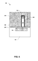
- FIG. 6 illustrates a portion of a semiconductor device, according to an embodiment
- FIG. 7 illustrates a portion of a semiconductor device, according to an embodiment
- FIG. 8 illustrates a portion of a semiconductor device, according to an embodiment
- FIG. 9 illustrates a portion of a semiconductor device, according to an embodiment
- FIG. 10 illustrates a portion of a semiconductor device, according to an embodiment
- FIG. 11 illustrates a portion of a semiconductor device, according to an embodiment
- FIG. 12 illustrates forming a second type region associated with forming a semiconductor device, according to an embodiment
- FIG. 13 illustrates forming a first type region contact, a second type region contact, and a gate contact associated with forming a semiconductor device, according to an embodiment
- FIG. 14 illustrates a portion of a semiconductor device, according to an embodiment
- FIG. 15 illustrates a semiconductor device, according to an embodiment
- FIG. 16 illustrates a semiconductor device, according to an embodiment
- FIG. 17 illustrates a method of forming a semiconductor device, according to an embodiment.
- One or more techniques for forming a semiconductor device and resulting structures formed thereby are provided herein.
- FIG. 1 is a sectional view illustrating a semiconductor device 100 according to some embodiments.
- the semiconductor device 100 is formed upon a well region 102 .
- the well region 102 comprises a first conductivity type.
- the first conductivity type comprises an n-type, such that the well region 102 comprises an n-well.
- the first conductivity type of the well region 102 comprises a p-type, such that the well region 102 comprises a p-well.
- the well region 102 is formed within a substrate region (not shown).
- the substrate region comprises any number of semiconductor materials, such as, for example, silicon, polysilicon, germanium, etc., alone or in combination.
- the substrate region comprises an epitaxial layer, a silicon-on-insulator (SOI) structure, etc.
- the substrate region comprises an epitaxial layer, wafer, die formed from a wafer, etc.
- SOI silicon-on-insulator
- the semiconductor device 100 comprises a first type region 104 .
- the first type region 104 is disposed within the well region 102 .
- the first type region 104 is implanted in the well region 102 .
- the first type region 104 comprises a first conductivity type.
- the first conductivity type of the first type region 104 comprises a p-type material, p+ type material, p++ type material, p-type dopants such as Boron, Gallium, Indium, etc., alone or in combination.
- the first conductivity type of the first type region 104 comprises an n-type material, n+ type material, n++ type material, n-type dopants such as Phosphorous, Arsenic, Antimony, etc., alone or in combination.
- the first type region 104 comprises a source region.
- the first type region 104 comprises a drain region.
- the well region 102 and first type region 104 comprise different conductivity types.
- the well region 102 comprises a p-type material, p+ type material, p++ type material, p-type dopants such as Boron, Gallium, Indium, etc., alone or in combination and the first type region 104 comprises an n-type material, n+ type material, n++ type material, n-type dopants such as Phosphorous, Arsenic, Antimony, etc., alone or in combination.
- the well region 102 comprises an n-type material, n+ type material, n++ type material, n-type dopants such as Phosphorous, Arsenic, Antimony, etc., alone or in combination and the first type region 104 comprises a p-type material, p+ type material, p++ type material, p-type dopants such as Boron, Gallium, Indium, etc., alone or in combination.
- the semiconductor device 100 comprises a channel region 110 extending between a first end 112 and a second end 114 .
- the channel region 110 comprises any number of materials, such as, for example, silicon, polysilicon, germanium, SiGe, III-V semiconductors (GaAs, InAs, InGaAs, etc.) etc., alone or in combination.
- the channel region 110 projects from the first type region 104 .
- the channel region 110 is formed in any number of ways, such as by deposition, epitaxial growth, etching, etc., for example.
- the channel region 110 comprises a p-type material, p+ type material, p++ type material, etc.
- the channel region 110 comprises an n-type material, n+ type material, n++ type material, etc.
- the channel region 110 comprises a nanowire, such as a vertical nanowire, etc.
- a mask region 120 is formed over the channel region 110 .
- the mask region 120 includes any number of materials, including silicon oxide, silicon nitride, etc., alone or in combination. In some embodiments, the mask region 120 extends across the second end 114 of the channel region 110 .
- a first dielectric region 200 is formed over the well region 102 , the first type region 104 , the channel region 110 , and the mask region 120 .
- the first dielectric region 200 is formed in any number of ways, such as by deposition, chemical vapor deposition (CVD), spin-on, or other suitable methods, for example.
- the first dielectric region 200 comprises any number of materials, including, for example, oxides, silicon dioxide, silicon nitride, silicon oxynitride, etc., alone or in combination.
- a top surface 202 of the first dielectric region 200 is planarized, such as by a chemical mechanical polishing (CMP) process.
- CMP chemical mechanical polishing
- the top surface 202 of the first dielectric region 200 is substantially co-planar with respect to a top surface 204 of the mask region 120 .
- dopants from the first type region 104 diffuse at least partially into the first end 112 of the channel region 110 .
- a diffusion portion 220 of the first type region 104 is formed extending from the first type region 104 into the channel region 110 .
- the diffusion portion 220 of the first type region 104 comprises the first conductivity type.
- the diffusion portion 220 of the first type region 104 comprises a first type region edge 250 .
- the first dielectric region 200 is patterned.
- the first dielectric region 200 is patterned by etching.
- the first dielectric region 200 is patterned to a first height 300 .
- the first height 300 of the first dielectric region 200 substantially matches a second height 302 of the diffusion portion 220 of the first type region 104 .
- a top surface 310 of the first dielectric region 200 is substantially co-planar with respect to the first type region edge 250 of the first type region 104 .
- a gate dielectric layer 400 is formed over the channel region 110 , mask region 120 , and first dielectric region 200 .
- the gate dielectric layer 400 is formed in any number of ways, such as by atomic layer deposition (ALD), chemical vapor deposition (CVD), physical vapor deposition (PVD), or other suitable techniques, for example.
- the gate dielectric layer 400 comprises any number of materials, including, in some embodiments, high-k dielectric materials, oxides, silicon dioxide, etc., alone or in combination.
- the gate dielectric layer 400 comprises a standard dielectric material with a medium dielectric constant, such as SiO 2 .
- the gate dielectric layer 400 is patterned. In some embodiments, the gate dielectric layer 400 is patterned such that the gate dielectric layer 400 does not cover the first dielectric region 200 . In an embodiment, the gate dielectric layer 400 is patterned such that a first end 402 of the gate dielectric layer 400 is located adjacent the first type region edge 250 . In an embodiment, a second end 404 of the gate dielectric layer 400 is located adjacent the first type region edge 250 on an opposite side of the channel region 110 . In an embodiment, the gate dielectric layer 400 covers the channel region 110 and the mask region 120 .
- a gate electrode 500 is formed over the first dielectric region 200 and the gate dielectric layer 400 .
- the gate electrode 500 is formed in any number of ways, such as by deposition, atomic layer deposition (ALD), etc., for example.
- the gate electrode 500 includes a conductive material, such as aluminum, copper, TiN, TaN, TaC, polysilicon, etc., alone or in combination.
- the gate dielectric layer 400 is not patterned but, instead, is left intact before formation of the gate electrode 500 .
- a second dielectric region 600 is formed over the gate electrode 500 .
- the second dielectric region 600 is formed in any number of ways, such as by deposition, chemical vapor deposition (CVD), or other suitable methods, for example.
- the second dielectric region 600 comprises any number of materials, including, for example, oxides, silicon dioxide, silicon nitride, silicon oxynitride, etc., alone or in combination.
- the second dielectric region 600 is made planar using a technique such as a chemical-mechanical polishing (CMP).
- CMP chemical-mechanical polishing
- portions of the gate dielectric layer 400 , gate electrode 500 , and second dielectric region 600 are removed, such as by etching.
- a top surface 610 of the gate dielectric layer 400 , a top surface 620 of the gate electrode 500 , and a top surface 630 of the second dielectric region 600 are substantially co-planar.
- the top surfaces 610 , 620 , 630 are substantially co-planar with respect to a second end channel surface 640 defined at the second end 114 of the channel region 110 .
- the mask region 120 is exposed above the gate dielectric layer 400 , gate electrode 500 , and second dielectric region 600 .
- the second dielectric region 600 along with portions of the gate dielectric layer 400 and gate electrode 500 , are removed, such as by etching.
- a top surface 800 of the gate electrode 500 and a top surface 802 of the gate dielectric layer 400 are planarized.
- a first portion 900 (illustrated in FIG. 8 ) of the gate electrode 500 is removed, such as by etching.
- the first portion 900 is located on a first side 902 of the channel region 110 .
- a first gate portion 910 is located on the first side 902 of the channel region 110 and a second gate portion 920 is located on a second side 904 of the channel region 110 .
- the gate electrode 500 surrounds the channel region 110 (illustrated in FIG. 14 ), such that the semiconductor device 100 comprises a gate-all-around structure.
- FIG. 10 illustrates the formation of the first dielectric region 200 , or, rather, additional first dielectric material above the existing first dielectric region 200 (illustrated in FIG. 9 ) and the gate electrode 500 .
- the first dielectric region 200 is formed on top of the first gate portion 910 and second gate portion 920 of the gate electrode 500 and over the gate dielectric layer 400 .
- the top surface 202 of the first dielectric region 200 is substantially co-planar with respect to the top surface 204 of the mask region 120 .
- an opening 1100 is formed in the first dielectric region 200 .
- the opening 1100 is formed by removing the mask region 120 .
- the mask region 120 is removed in any number of ways, such as by etching, for example.
- the opening 1100 is formed to the second end channel surface 640 at the second end 114 of the channel region 110 .
- the opening 1100 is formed such that sidewalls 1102 defining the opening 118 are located in line with and above sides 1110 of the channel region 110 .
- a second type region 1200 is formed.
- the second type region 1200 is formed in any number of ways.
- the second type region 1200 is formed by doping the second end 114 of the channel region 110 .
- the second type region 1200 comprises a second conductivity type.
- the second conductivity type of the second type region 1200 comprises a p-type material, p+ type material, p++ type material, p-type dopants such as Boron, Gallium, Indium, etc., alone or in combination.
- the second conductivity type of the second type region 1200 comprises an n-type material, n+ type material, n++ type material, n-type dopants such as Phosphorous, Arsenic, Antimony, etc., alone or in combination.
- the second type region 1200 comprises a source region.
- doping of the second type region 1200 is achieved using implantation, plasma doping, deposition of doped silicide, or any other method(s).
- the second type region 1200 is formed using doped epitaxy or selective epitaxy.
- the second type region 1200 comprises a drain region.
- the first conductivity type of the first type region 104 is substantially similar to the second conductivity type of the second type region 1200 .
- the first conductivity type of the first type region 104 and the second conductivity type of the second type region 1200 comprise a p-type material, p+ type material, p++ type material, p-type dopants such as Boron, Gallium, Indium, etc., alone or in combination.
- the first conductivity type of the first type region 104 and the second conductivity type of the second type region 1200 comprise an n-type material, n+ type material, n++ type material, n-type dopants such as Phosphorous, Arsenic, Antimony, etc., alone or in combination.
- a drift region 1201 exists between the channel region 110 and the second type region 1200 .
- the drift region 1201 comprises a material or composition similar to a material or composition of the channel region 110 .
- the drift region 1201 extends between the channel region 110 and the second type region 1200 .
- the channel region 110 extends between the first type region 104 and the second type region 1200 and is substantially surrounded by the gate electrode 500 .
- a channel length 1210 of the channel region 110 is measured between the first type region edge 250 of the first type region 104 and the drift region 1201 .
- the channel length 1210 of the channel region 110 is between about 5 nm to about 40 nm.
- the gate electrode 500 extends between a first gate edge 1230 and a second gate edge 1232 .
- the gate electrode 500 comprises a gate length 1234 measured between the first gate edge 1230 and the second gate edge 1232 .
- the gate length 1234 of the gate electrode 500 is between about 5 nm to about 25 nm.
- the gate length 1234 of the gate electrode 500 substantially matches the channel length 1210 of the channel region 110 .
- the gate electrode 500 is separated from the first type region 104 .
- the first gate edge 1230 of the gate electrode 500 is separated a first distance 1231 from the first type region edge 250 of the first type region 104 .
- the first distance 1231 is between 0 nm to about 3 nm.
- the first gate edge 1230 is substantially co-planar with and not spaced apart from the first type region edge 250 , such that the first distance 1231 is about 0 nm. In some embodiments, not illustrated in FIG.
- the gate electrode 500 overlaps at least some of the diffusion portion 220 of the first type region 104 , such that the first gate edge 1230 of the gate electrode 500 is not co-planar with the first type region edge, but is instead located below first type region edge 250 .
- the gate electrode 500 is separated from the second type region 1200 .
- the second gate edge 1232 of the gate electrode 500 is separated a second distance 1240 from the second type region edge 1220 of the second type region 1200 .
- the second distance 1240 is between about 2 nm to about 7 nm.
- the second distance 1240 is about 20% to about 70% of the channel length 1210 of the channel region 110 .
- the first distance 1231 is less than the second distance 1240 .
- the second distance 1240 substantially matches a length of the drift region 1201 .
- the first dielectric region 200 is patterned to form a plurality of openings for a first type region contact 1300 , second type region contact 1302 , and a gate contact 1304 .
- the first type region contact 1300 , second type region contact 1302 , and gate contact 1304 comprise a conductive material.
- the first type region contact 1300 is formed in contact with the first type region 104 .
- the second type region contact 1302 is formed in contact with the second type region 1200 .
- the gate contact 1304 is formed in contact with the gate electrode 500 .
- V g a sufficient voltage
- FIG. 14 is a perspective view of an embodiment of the semiconductor device 100 , but where the well region 102 , first dielectric region 200 , first type region contact 1300 , second type region contact 1302 , gate contact 1304 , and first type region 104 , other than diffusion portion 220 , are not illustrated.
- the gate electrode 500 surrounds at least some of the channel region 110 .
- the gate electrode 500 comprises the gate length 1234 and, thus, surrounds a length of the channel region 110 that corresponds to the gate length 1234 .
- the gate dielectric layer 400 also surrounds the channel region 110 and has a length corresponding to the gate length 1234 .
- the second gate edge 1232 of the gate electrode 500 is separated by the second distance 1240 from the second type region edge 1220 of the second type region 1200 .
- the first distance 1231 is less than the second distance 1240 .
- the gate electrode 500 is closer to one of the first type region 104 (illustrated as the diffusion portion 220 of the first type region 104 ) or the second type region 1200 , such that the semiconductor device 100 comprises an asymmetric semiconductor device.
- FIG. 15 illustrates a second example semiconductor device 1500 .
- the second semiconductor device 1500 is formed on a substrate region 1502 .
- the substrate region 1502 comprises any number of materials, such as, for example, silicon, polysilicon, germanium, III—V alloy semiconductors such as GaAs, InAs, InGaAs, etc., alone or in combination.
- the substrate region 1502 comprises an epitaxial layer, wafer, die formed from a wafer, etc.
- the second semiconductor device 1500 comprises a finFET device.
- the second semiconductor device 1500 comprises a fin 1504 formed on the substrate region 1502 .
- a channel region 1510 is comprised within a portion of the fin 1504 .
- the channel region 1510 comprises a p-type material, p+ type material, p++ type material, p-type dopants such as Boron, Indium, Gallium, etc., alone or in combination.
- the channel region 1510 comprises an n-type material, n+ type material, n++ type material, n-type dopants such as Phosphorous, Arsenic, Antimony, etc., alone or in combination.
- the second semiconductor device 1500 comprises a first type region 1520 formed on the substrate region 1502 .
- the first type region 1520 comprises a first portion of the fin 1504 .
- the first type region 1520 is located on a first side of the channel region 1510 .
- the first type region 1520 comprises a first conductivity type.
- the first conductivity type of the first type region 1520 comprises a p-type material, p+ type material, p++ type material, p-type dopants such as Boron, Indium, Gallium, etc., alone or in combination.
- the first conductivity type of the first type region 1520 comprises an n-type material, n+ type material, n++ type material, n-type dopants such as Phosphorous, Arsenic, Antimony, etc., alone or in combination.
- the first type region 1520 comprises a source region.
- the first type region 1520 comprises a drain region.
- the second semiconductor device 1500 comprises a drift region 1511 that exists on the substrate region 1502 .
- the drift region 1511 extends between the channel region 1510 and a second type region 1530 .
- the drift region 1511 comprises a material or material or composition similar to that of the channel region 1510 .
- the second semiconductor device 1500 comprises the second type region 1530 formed on the substrate region 1502 .
- the second type region 1530 comprises a second portion of the fin 1504 .
- the second type region 1530 is located on a second side of the channel region 1510 opposite the first side of the channel region 1510 .
- the channel region 1510 extends between the first type region 1520 and the second type region 1530 , with the drift region 1511 extending between the channel region 1510 and the second type region 1530 .
- the second type region 1530 comprises a second conductivity type.
- the second conductivity type of the second type region 1530 comprises a p-type material, p+ type material, p++ type material, p-type dopants such as Boron, Indium, Gallium, etc., alone or in combination.
- the second conductivity type of the second type region 1530 comprises an n-type material, n+ type material, n++ type material, n-type dopants such as Phosphorous, Arsenic, Antimony, alone or in combination.
- the second type region 1530 comprises a source region.
- the second type region 1530 comprises a drain region.
- the first conductivity type of the first type region 1520 is substantially similar to the second conductivity type of the second type region 1530 .
- the first conductivity type of the first type region 1520 and the second conductivity type of the second type region 1530 comprise a p-type material, p+ type material, p++ type material, p-type dopants such as Boron, Gallium, Indium, etc., alone or in combination.
- the first conductivity type of the first type region 1520 and the second conductivity type of the second type region 1530 comprise an n-type material, n+ type material, n++ type material, n-type dopants such as Phosphorous, Arsenic, Antimony, etc., alone or in combination.
- the second semiconductor device 1500 comprises a gate electrode 1540 surrounding at least some of the channel region 1510 .
- the semiconductor device 1500 also comprises, in some embodiments, a gate dielectric layer disposed between the channel region 1510 and the gate electrode 1540 to electrically isolate the channel region 1510 from the gate dielectric layer.
- the gate dielectric layer is formed in any suitable manner of any suitable material having any suitable dielectric constant.
- the gate electrode 1540 is formed in any number of ways, such as by deposition, epitaxial growth, etc., for example.
- the gate electrode 1540 includes a conductive material, such as aluminum, polysilicon, TiN, TaC, TaN, etc., alone or in combination.
- the gate electrode 1540 extends between a first gate edge 1550 and a second gate edge 1552 .
- the gate electrode 1540 comprises a gate length 1554 measured between the first gate edge 1550 and the second gate edge 1552 .
- the gate length 1554 of the gate electrode 1540 is between about 5 nm to about 25 nm.
- the gate electrode 1540 is separated from the first type region 1520 .
- the first gate edge 1550 of the gate electrode 1540 is separated a first distance 1560 from a first type region edge 1562 of the first type region 1520 .
- the first distance 1560 is between 0 nm to about 1 nm.
- the first gate edge 1550 is substantially adjacent to and not spaced apart from the first type region edge 1562 , such that the first distance 1560 is about 0 nm.
- the gate electrode 1540 is separated from the second type region 1530 .
- the second gate edge 1552 is separated a second distance 1570 from a second type region edge 1572 of the second type region 1530 .
- the second distance 1570 is between about 2 nm to about 7 nm.
- the second distance 1570 is about 20% to about 70% of a channel length 1580 of the channel region 110 .
- the first distance 1560 is less than the second distance 1570 .
- the second distance 1570 substantially matches a length of the drift region 1511 .
- the channel length 1580 of the channel region 1510 is between about 20 nm to about 40 nm. In an embodiment, the channel length 1580 of the channel region 1510 is measured between the first type region edge 1562 of the first type region 1520 and the drift region 1511 . In some embodiments, the gate length 1554 of the gate electrode 1540 substantially matches the channel length 1580 of the channel region 1510 .
- FIG. 16 illustrates a third example semiconductor device 1600 .
- the third semiconductor device 1600 comprises the channel region 1510 , first type region 1520 , second type region 1530 , gate dielectric layer, and the gate electrode 1540 .
- the third semiconductor device 1600 is formed on a substrate region 1602 .
- the substrate region 1602 comprises a silicon-on-insulator (SOI) structure.
- the substrate region 1602 comprises an insulator layer 1604 .
- the insulator layer 1604 includes any number of materials, including oxides, SiO 2 , etc.
- the insulator layer 1604 is formed on a substrate layer 1606 .
- the substrate layer 1606 includes any number of materials, including silicon, polysilicon, germanium, etc., alone or in combination.
- the semiconductor device 100 , 1500 , 1600 is asymmetric due to the gate electrode 500 , 1540 being located a shorter distance to one of the first type region 104 , 1520 or the second type region 1200 , 1530 as compared to the other type region.
- the semiconductor device 100 , 1500 , 1600 exhibits reduced short channel effects through the channel region 110 , 1510 as compared to a non-asymmetric device.
- the semiconductor device 100 , 1500 , 1600 exhibits a current drive through the channel region 110 , 1510 that is equal to or greater than a current drive in a non-asymmetric device.
- FIG. 17 An example method 1700 of forming a semiconductor device, such as semiconductor device 100 , 1500 , 1600 , according to some embodiments, is illustrated in FIG. 17 .
- the first type region 104 , 1520 is formed comprising the first conductivity type.
- the second type region 1200 , 1530 is formed comprising the second conductivity type.
- the channel region 110 , 1510 is formed between the first type region 104 , 1520 and the second type region 1200 , 1530 .
- the gate electrode 500 , 1540 is formed surrounding at least some of the channel region 110 , 1510 , with the first gate edge 1230 , 1550 of the gate electrode 500 , 1540 separated the first distance 1231 , 1560 from the first type region edge 250 , 1562 of the first type region 104 , 1520 and the second gate edge 1232 , 1552 of the gate electrode 500 , 1540 separated the second distance 1240 , 1570 from the second type region edge 1220 , 1572 of the second type region 1200 , 1530 , wherein the first distance 1231 , 1560 is less than the second distance 1240 , 1570 .
- a semiconductor device comprises a first type region comprising a first conductivity type and a second type region comprising a second conductivity type.
- the semiconductor device comprises a channel region extending between the first type region and the second type region.
- the semiconductor device comprises a gate electrode surrounding at least some of the channel region.
- a first gate edge of the gate electrode is separated a first distance from a first type region edge of the first type region and a second gate edge of the gate electrode is separated a second distance from a second type region edge of the second type region.
- the first distance is less than the second distance.
- the semiconductor device comprises a first type region comprising a first conductivity type and a second type region comprising a second conductivity type.
- the semiconductor device comprises a channel region extending between the first type region and the second type region.
- the semiconductor device comprises a gate electrode surrounding at least some of the channel region.
- a second gate edge of the gate electrode is separated a second distance from a second type region edge of the second type region. In an embodiment, the second distance is about 20% to about 70% of a channel length of the channel region.
- a method of forming a semiconductor device comprises forming a first type region comprising a first conductivity type. In an embodiment, the method comprises forming a second type region comprising a second conductivity type. In an embodiment, the method comprises forming a channel region between the first type region and the second type region. In an embodiment, the method comprises forming a gate electrode surrounding at least some of the channel region. In an embodiment, a first gate edge of the gate electrode is separated a first distance from a first type region edge of the first type region and a second gate edge of the gate electrode is separated a second distance from a second type region edge of the second type region. In an embodiment, the first distance is less than the second distance.
- exemplary is used herein to mean serving as an example, instance, illustration, etc., and not necessarily as advantageous.
- “or” is intended to mean an inclusive “or” rather than an exclusive “or”.
- “a” and “an” as used in this application and the appended claims are generally be construed to mean “one or more” unless specified otherwise or clear from context to be directed to a singular form.
- at least one of A and B and/or the like generally means A or B or both A and B.
- such terms are intended to be inclusive in a manner similar to the term “comprising”.
- first,” “second,” or the like are not intended to imply a temporal aspect, a spatial aspect, an ordering, etc. Rather, such terms are merely used as identifiers, names, etc. for features, elements, items, etc.
- a first type region and a second type region generally correspond to first type region A and second type region B or two different or two identical type regions or the same type region.
Abstract
A semiconductor device includes a first type region including a first conductivity type and a second type region including a second conductivity type. The semiconductor device includes a channel region extending between the first type region and the second type region. The semiconductor device includes a gate electrode surrounding at least some of the channel region. A first gate edge of the gate electrode is separated a first distance from a first type region edge of the first type region and a second gate edge of the gate electrode is separated a second distance from a second type region edge of the second type region. The first distance is less than the second distance.
Description
This application is a divisional of and claims priority to U.S. patent application Ser. No. 14/032,153, having an amended title of “SEMICONDUCTOR DEVICE HAVING GATE DIELECTRIC SURROUNDING AT LEAST SOME OF CHANNEL REGION AND GATE ELECTRODE SURROUNDING AT LEAST SOME OF GATE DIELECTRIC” and filed on Sep. 19, 2013, which is incorporated herein by reference.
In a semiconductor device, current flows through a channel region between a source region and a drain region upon application of a sufficient voltage or bias to a gate of the device. When current flows through the channel region, the device is generally regarded as being in an ‘on’ state, and when current is not flowing through the channel region, the device is generally regarded as being in an ‘off’ state.
This summary is provided to introduce a selection of concepts in a simplified form that are further described below in the detailed description. This summary is not intended to be an extensive overview of the claimed subject matter, identify key factors or essential features of the claimed subject matter, nor is it intended to be used to limit the scope of the claimed subject matter.
One or more techniques, and resulting structures, for forming a semiconductor device are provided herein.
The following description and annexed drawings set forth certain illustrative aspects and implementations. These are indicative of but a few of the various ways in which one or more aspects are employed. Other aspects, advantages, and/or novel features of the disclosure will become apparent from the following detailed description when considered in conjunction with the annexed drawings.
Aspects of the disclosure are understood from the following detailed description when read with the accompanying drawings. It will be appreciated that elements and/or structures of the drawings are not necessarily be drawn to scale. Accordingly, the dimensions of the various features may be arbitrarily increased and/or reduced for clarity of discussion.
The claimed subject matter is now described with reference to the drawings, wherein like reference numerals are generally used to refer to like elements throughout. In the following description, for purposes of explanation, numerous specific details are set forth in order to provide an understanding of the claimed subject matter. It is evident, however, that the claimed subject matter may be practiced without these specific details. In other instances, structures and devices are illustrated in block diagram form in order to facilitate describing the claimed subject matter.
One or more techniques for forming a semiconductor device and resulting structures formed thereby are provided herein.
In an embodiment, the semiconductor device 100 comprises a first type region 104. According to some embodiments, the first type region 104 is disposed within the well region 102. In an embodiment, the first type region 104 is implanted in the well region 102. In an embodiment, the first type region 104 comprises a first conductivity type. In some embodiments, the first conductivity type of the first type region 104 comprises a p-type material, p+ type material, p++ type material, p-type dopants such as Boron, Gallium, Indium, etc., alone or in combination. In some embodiments, the first conductivity type of the first type region 104 comprises an n-type material, n+ type material, n++ type material, n-type dopants such as Phosphorous, Arsenic, Antimony, etc., alone or in combination. According to some embodiments, the first type region 104 comprises a source region. According to some embodiments, the first type region 104 comprises a drain region. In some embodiments, the well region 102 and first type region 104 comprise different conductivity types. In some embodiments, the well region 102 comprises a p-type material, p+ type material, p++ type material, p-type dopants such as Boron, Gallium, Indium, etc., alone or in combination and the first type region 104 comprises an n-type material, n+ type material, n++ type material, n-type dopants such as Phosphorous, Arsenic, Antimony, etc., alone or in combination. In some embodiments, the well region 102 comprises an n-type material, n+ type material, n++ type material, n-type dopants such as Phosphorous, Arsenic, Antimony, etc., alone or in combination and the first type region 104 comprises a p-type material, p+ type material, p++ type material, p-type dopants such as Boron, Gallium, Indium, etc., alone or in combination.
According to some embodiments, the semiconductor device 100 comprises a channel region 110 extending between a first end 112 and a second end 114. The channel region 110 comprises any number of materials, such as, for example, silicon, polysilicon, germanium, SiGe, III-V semiconductors (GaAs, InAs, InGaAs, etc.) etc., alone or in combination. In some embodiments, the channel region 110 projects from the first type region 104. The channel region 110 is formed in any number of ways, such as by deposition, epitaxial growth, etching, etc., for example. In some embodiments, the channel region 110 comprises a p-type material, p+ type material, p++ type material, etc. In some embodiments, the channel region 110 comprises an n-type material, n+ type material, n++ type material, etc. In an embodiment, the channel region 110 comprises a nanowire, such as a vertical nanowire, etc.
According to some embodiments, a mask region 120 is formed over the channel region 110. The mask region 120 includes any number of materials, including silicon oxide, silicon nitride, etc., alone or in combination. In some embodiments, the mask region 120 extends across the second end 114 of the channel region 110.
Turning now to FIG. 2 , in an embodiment, a first dielectric region 200 is formed over the well region 102, the first type region 104, the channel region 110, and the mask region 120. The first dielectric region 200 is formed in any number of ways, such as by deposition, chemical vapor deposition (CVD), spin-on, or other suitable methods, for example. The first dielectric region 200 comprises any number of materials, including, for example, oxides, silicon dioxide, silicon nitride, silicon oxynitride, etc., alone or in combination. In some embodiments, a top surface 202 of the first dielectric region 200 is planarized, such as by a chemical mechanical polishing (CMP) process. In an embodiment, the top surface 202 of the first dielectric region 200 is substantially co-planar with respect to a top surface 204 of the mask region 120.
According to some embodiments, dopants from the first type region 104 diffuse at least partially into the first end 112 of the channel region 110. In some embodiments, a diffusion portion 220 of the first type region 104 is formed extending from the first type region 104 into the channel region 110. In an embodiment, the diffusion portion 220 of the first type region 104 comprises the first conductivity type. In some embodiments, the diffusion portion 220 of the first type region 104 comprises a first type region edge 250.
Turning now to FIG. 3 , in an embodiment, the first dielectric region 200 is patterned. In some embodiments, the first dielectric region 200 is patterned by etching. According to some embodiments, the first dielectric region 200 is patterned to a first height 300. In some embodiments, the first height 300 of the first dielectric region 200 substantially matches a second height 302 of the diffusion portion 220 of the first type region 104. In an embodiment, a top surface 310 of the first dielectric region 200 is substantially co-planar with respect to the first type region edge 250 of the first type region 104.
Turning now to FIG. 4 , in an embodiment, a gate dielectric layer 400 is formed over the channel region 110, mask region 120, and first dielectric region 200. The gate dielectric layer 400 is formed in any number of ways, such as by atomic layer deposition (ALD), chemical vapor deposition (CVD), physical vapor deposition (PVD), or other suitable techniques, for example. The gate dielectric layer 400 comprises any number of materials, including, in some embodiments, high-k dielectric materials, oxides, silicon dioxide, etc., alone or in combination. According to some embodiments, the gate dielectric layer 400 comprises a standard dielectric material with a medium dielectric constant, such as SiO2.
Turning now to FIG. 5 , in an embodiment, the gate dielectric layer 400 is patterned. In some embodiments, the gate dielectric layer 400 is patterned such that the gate dielectric layer 400 does not cover the first dielectric region 200. In an embodiment, the gate dielectric layer 400 is patterned such that a first end 402 of the gate dielectric layer 400 is located adjacent the first type region edge 250. In an embodiment, a second end 404 of the gate dielectric layer 400 is located adjacent the first type region edge 250 on an opposite side of the channel region 110. In an embodiment, the gate dielectric layer 400 covers the channel region 110 and the mask region 120.
According to some embodiments, a gate electrode 500 is formed over the first dielectric region 200 and the gate dielectric layer 400. The gate electrode 500 is formed in any number of ways, such as by deposition, atomic layer deposition (ALD), etc., for example. In some embodiments, the gate electrode 500 includes a conductive material, such as aluminum, copper, TiN, TaN, TaC, polysilicon, etc., alone or in combination. In some embodiments, the gate dielectric layer 400 is not patterned but, instead, is left intact before formation of the gate electrode 500.
Turning now to FIG. 6 , in an embodiment, a second dielectric region 600 is formed over the gate electrode 500. The second dielectric region 600 is formed in any number of ways, such as by deposition, chemical vapor deposition (CVD), or other suitable methods, for example. The second dielectric region 600 comprises any number of materials, including, for example, oxides, silicon dioxide, silicon nitride, silicon oxynitride, etc., alone or in combination. In an embodiment, the second dielectric region 600 is made planar using a technique such as a chemical-mechanical polishing (CMP).
Turning now to FIG. 7 , in some embodiments, portions of the gate dielectric layer 400, gate electrode 500, and second dielectric region 600 are removed, such as by etching. According to some embodiments, a top surface 610 of the gate dielectric layer 400, a top surface 620 of the gate electrode 500, and a top surface 630 of the second dielectric region 600 are substantially co-planar. According to some embodiments, after portions of the gate dielectric layer 400, gate electrode 500, and second dielectric region 600 are removed, the top surfaces 610, 620, 630, are substantially co-planar with respect to a second end channel surface 640 defined at the second end 114 of the channel region 110. In some embodiments, after portions of the gate dielectric layer 400, gate electrode 500, and second dielectric region 600 are removed, the mask region 120 is exposed above the gate dielectric layer 400, gate electrode 500, and second dielectric region 600.
Turning now to FIG. 8 , in some embodiments, the second dielectric region 600, along with portions of the gate dielectric layer 400 and gate electrode 500, are removed, such as by etching. According to some embodiments, a top surface 800 of the gate electrode 500 and a top surface 802 of the gate dielectric layer 400 are planarized.
Turning now to FIG. 9 , in some embodiments, a first portion 900 (illustrated in FIG. 8 ) of the gate electrode 500 is removed, such as by etching. According to some embodiments, the first portion 900 is located on a first side 902 of the channel region 110. In some embodiments, after removal of the first portion 900, a first gate portion 910 is located on the first side 902 of the channel region 110 and a second gate portion 920 is located on a second side 904 of the channel region 110. According to some embodiments, the gate electrode 500 surrounds the channel region 110 (illustrated in FIG. 14 ), such that the semiconductor device 100 comprises a gate-all-around structure.
Turning to FIG. 11 , in an embodiment, an opening 1100 is formed in the first dielectric region 200. In some embodiments, the opening 1100 is formed by removing the mask region 120. The mask region 120 is removed in any number of ways, such as by etching, for example. According to some embodiments, the opening 1100 is formed to the second end channel surface 640 at the second end 114 of the channel region 110. In some embodiments, the opening 1100 is formed such that sidewalls 1102 defining the opening 118 are located in line with and above sides 1110 of the channel region 110.
Turning now to FIG. 12 , in some embodiments, a second type region 1200 is formed. The second type region 1200 is formed in any number of ways. According to some embodiments, the second type region 1200 is formed by doping the second end 114 of the channel region 110. According to some embodiments, the second type region 1200 comprises a second conductivity type. In some embodiments, the second conductivity type of the second type region 1200 comprises a p-type material, p+ type material, p++ type material, p-type dopants such as Boron, Gallium, Indium, etc., alone or in combination. In some embodiments, the second conductivity type of the second type region 1200 comprises an n-type material, n+ type material, n++ type material, n-type dopants such as Phosphorous, Arsenic, Antimony, etc., alone or in combination. According to some embodiments, the second type region 1200 comprises a source region. In an embodiment, doping of the second type region 1200 is achieved using implantation, plasma doping, deposition of doped silicide, or any other method(s). In an embodiment, the second type region 1200 is formed using doped epitaxy or selective epitaxy. According to some embodiments, the second type region 1200 comprises a drain region.
According to some embodiments, the first conductivity type of the first type region 104 is substantially similar to the second conductivity type of the second type region 1200. In an embodiment, the first conductivity type of the first type region 104 and the second conductivity type of the second type region 1200 comprise a p-type material, p+ type material, p++ type material, p-type dopants such as Boron, Gallium, Indium, etc., alone or in combination. In an embodiment, the first conductivity type of the first type region 104 and the second conductivity type of the second type region 1200 comprise an n-type material, n+ type material, n++ type material, n-type dopants such as Phosphorous, Arsenic, Antimony, etc., alone or in combination.
In some embodiments, after the second type region 1200 is formed, a drift region 1201 exists between the channel region 110 and the second type region 1200. According to some embodiments, the drift region 1201 comprises a material or composition similar to a material or composition of the channel region 110. In an embodiment, the drift region 1201 extends between the channel region 110 and the second type region 1200.
In some embodiments, the channel region 110 extends between the first type region 104 and the second type region 1200 and is substantially surrounded by the gate electrode 500. In an embodiment, a channel length 1210 of the channel region 110 is measured between the first type region edge 250 of the first type region 104 and the drift region 1201. According to some embodiments, the channel length 1210 of the channel region 110 is between about 5 nm to about 40 nm.
According to some embodiments, the gate electrode 500 extends between a first gate edge 1230 and a second gate edge 1232. In an embodiment, the gate electrode 500 comprises a gate length 1234 measured between the first gate edge 1230 and the second gate edge 1232. In an embodiment, the gate length 1234 of the gate electrode 500 is between about 5 nm to about 25 nm. In some embodiments, the gate length 1234 of the gate electrode 500 substantially matches the channel length 1210 of the channel region 110.
According to some embodiments, the gate electrode 500 is separated from the first type region 104. In some embodiments, the first gate edge 1230 of the gate electrode 500 is separated a first distance 1231 from the first type region edge 250 of the first type region 104. In some embodiments, the first distance 1231 is between 0 nm to about 3 nm. In an embodiment, as illustrated in FIG. 12 , the first gate edge 1230 is substantially co-planar with and not spaced apart from the first type region edge 250, such that the first distance 1231 is about 0 nm. In some embodiments, not illustrated in FIG. 12 , the gate electrode 500 overlaps at least some of the diffusion portion 220 of the first type region 104, such that the first gate edge 1230 of the gate electrode 500 is not co-planar with the first type region edge, but is instead located below first type region edge 250.
According to some embodiments, the gate electrode 500 is separated from the second type region 1200. In some embodiments, the second gate edge 1232 of the gate electrode 500 is separated a second distance 1240 from the second type region edge 1220 of the second type region 1200. In some embodiments, the second distance 1240 is between about 2 nm to about 7 nm. In some embodiments, the second distance 1240 is about 20% to about 70% of the channel length 1210 of the channel region 110. According to some embodiments, the first distance 1231 is less than the second distance 1240. According to some embodiments, the second distance 1240 substantially matches a length of the drift region 1201.
Turning now to FIG. 13 , according to some embodiments, the first dielectric region 200 is patterned to form a plurality of openings for a first type region contact 1300, second type region contact 1302, and a gate contact 1304. In an embodiment, the first type region contact 1300, second type region contact 1302, and gate contact 1304 comprise a conductive material. In some embodiments, the first type region contact 1300 is formed in contact with the first type region 104. In some embodiments, the second type region contact 1302 is formed in contact with the second type region 1200. In some embodiments, the gate contact 1304 is formed in contact with the gate electrode 500. According to some embodiments, when a sufficient voltage (Vg) is applied to the gate contact 1304, current will flow through the channel region 110 between the first type region 104 and the second type region 1200 and thus between the first type region contact 1300 and the second type region contact 1302.
In an embodiment, the gate electrode 500 surrounds at least some of the channel region 110. In some embodiments, the gate electrode 500 comprises the gate length 1234 and, thus, surrounds a length of the channel region 110 that corresponds to the gate length 1234. In some embodiments, the gate dielectric layer 400 also surrounds the channel region 110 and has a length corresponding to the gate length 1234. In some embodiments, the second gate edge 1232 of the gate electrode 500 is separated by the second distance 1240 from the second type region edge 1220 of the second type region 1200. According to some embodiments, the first distance 1231 is less than the second distance 1240. Accordingly, in some embodiments, the gate electrode 500 is closer to one of the first type region 104 (illustrated as the diffusion portion 220 of the first type region 104) or the second type region 1200, such that the semiconductor device 100 comprises an asymmetric semiconductor device.
According to some embodiments, the second semiconductor device 1500 comprises a finFET device. In an embodiment, the second semiconductor device 1500 comprises a fin 1504 formed on the substrate region 1502. In some examples, a channel region 1510 is comprised within a portion of the fin 1504. In some embodiments, the channel region 1510 comprises a p-type material, p+ type material, p++ type material, p-type dopants such as Boron, Indium, Gallium, etc., alone or in combination. In some embodiments, the channel region 1510 comprises an n-type material, n+ type material, n++ type material, n-type dopants such as Phosphorous, Arsenic, Antimony, etc., alone or in combination.
According to some embodiments, the second semiconductor device 1500 comprises a first type region 1520 formed on the substrate region 1502. According to some embodiments, the first type region 1520 comprises a first portion of the fin 1504. In some embodiments, the first type region 1520 is located on a first side of the channel region 1510. In some embodiments, the first type region 1520 comprises a first conductivity type. In some embodiments, the first conductivity type of the first type region 1520 comprises a p-type material, p+ type material, p++ type material, p-type dopants such as Boron, Indium, Gallium, etc., alone or in combination. In some embodiments, the first conductivity type of the first type region 1520 comprises an n-type material, n+ type material, n++ type material, n-type dopants such as Phosphorous, Arsenic, Antimony, etc., alone or in combination. According to some embodiments, the first type region 1520 comprises a source region. According to some embodiments, the first type region 1520 comprises a drain region.
In some embodiments, the second semiconductor device 1500 comprises a drift region 1511 that exists on the substrate region 1502. According to some embodiments, the drift region 1511 extends between the channel region 1510 and a second type region 1530. According to some embodiments, the drift region 1511 comprises a material or material or composition similar to that of the channel region 1510.
According to some embodiments, the second semiconductor device 1500 comprises the second type region 1530 formed on the substrate region 1502. According to some embodiments, the second type region 1530 comprises a second portion of the fin 1504. In some embodiments, the second type region 1530 is located on a second side of the channel region 1510 opposite the first side of the channel region 1510. According to some embodiments, the channel region 1510 extends between the first type region 1520 and the second type region 1530, with the drift region 1511 extending between the channel region 1510 and the second type region 1530. In some embodiments, the second type region 1530 comprises a second conductivity type. In some embodiments, the second conductivity type of the second type region 1530 comprises a p-type material, p+ type material, p++ type material, p-type dopants such as Boron, Indium, Gallium, etc., alone or in combination. In some embodiments, the second conductivity type of the second type region 1530 comprises an n-type material, n+ type material, n++ type material, n-type dopants such as Phosphorous, Arsenic, Antimony, alone or in combination. According to some embodiments, the second type region 1530 comprises a source region. According to some embodiments, the second type region 1530 comprises a drain region.
According to some embodiments, the first conductivity type of the first type region 1520 is substantially similar to the second conductivity type of the second type region 1530. In an embodiment, the first conductivity type of the first type region 1520 and the second conductivity type of the second type region 1530 comprise a p-type material, p+ type material, p++ type material, p-type dopants such as Boron, Gallium, Indium, etc., alone or in combination. In an embodiment, the first conductivity type of the first type region 1520 and the second conductivity type of the second type region 1530 comprise an n-type material, n+ type material, n++ type material, n-type dopants such as Phosphorous, Arsenic, Antimony, etc., alone or in combination.
According to some embodiments, the second semiconductor device 1500 comprises a gate electrode 1540 surrounding at least some of the channel region 1510. Although not illustrated, the semiconductor device 1500 also comprises, in some embodiments, a gate dielectric layer disposed between the channel region 1510 and the gate electrode 1540 to electrically isolate the channel region 1510 from the gate dielectric layer. The gate dielectric layer is formed in any suitable manner of any suitable material having any suitable dielectric constant. The gate electrode 1540 is formed in any number of ways, such as by deposition, epitaxial growth, etc., for example. In some embodiments, the gate electrode 1540 includes a conductive material, such as aluminum, polysilicon, TiN, TaC, TaN, etc., alone or in combination.
According to some embodiments, the gate electrode 1540 extends between a first gate edge 1550 and a second gate edge 1552. In an embodiment, the gate electrode 1540 comprises a gate length 1554 measured between the first gate edge 1550 and the second gate edge 1552. In an embodiment, the gate length 1554 of the gate electrode 1540 is between about 5 nm to about 25 nm.
According to some embodiments, the gate electrode 1540 is separated from the first type region 1520. In some embodiments, the first gate edge 1550 of the gate electrode 1540 is separated a first distance 1560 from a first type region edge 1562 of the first type region 1520. In some embodiments, the first distance 1560 is between 0 nm to about 1 nm. In an embodiment, as illustrated in FIG. 15 , the first gate edge 1550 is substantially adjacent to and not spaced apart from the first type region edge 1562, such that the first distance 1560 is about 0 nm.
According to some embodiments, the gate electrode 1540 is separated from the second type region 1530. According to some embodiments, the second gate edge 1552 is separated a second distance 1570 from a second type region edge 1572 of the second type region 1530. In some embodiments, the second distance 1570 is between about 2 nm to about 7 nm. In some embodiments, the second distance 1570 is about 20% to about 70% of a channel length 1580 of the channel region 110. According to some embodiments, the first distance 1560 is less than the second distance 1570. According to some embodiments, the second distance 1570 substantially matches a length of the drift region 1511.
In some embodiments, the channel length 1580 of the channel region 1510 is between about 20 nm to about 40 nm. In an embodiment, the channel length 1580 of the channel region 1510 is measured between the first type region edge 1562 of the first type region 1520 and the drift region 1511. In some embodiments, the gate length 1554 of the gate electrode 1540 substantially matches the channel length 1580 of the channel region 1510.
According to some embodiments, the semiconductor device 100, 1500, 1600 is asymmetric due to the gate electrode 500, 1540 being located a shorter distance to one of the first type region 104, 1520 or the second type region 1200, 1530 as compared to the other type region. In some embodiments, the semiconductor device 100, 1500, 1600 exhibits reduced short channel effects through the channel region 110, 1510 as compared to a non-asymmetric device. Additionally, in some embodiments, the semiconductor device 100, 1500, 1600 exhibits a current drive through the channel region 110, 1510 that is equal to or greater than a current drive in a non-asymmetric device.
An example method 1700 of forming a semiconductor device, such as semiconductor device 100, 1500, 1600, according to some embodiments, is illustrated in FIG. 17 . At 1702, the first type region 104, 1520 is formed comprising the first conductivity type. At 1704, the second type region 1200, 1530 is formed comprising the second conductivity type. At 1706, the channel region 110, 1510 is formed between the first type region 104, 1520 and the second type region 1200, 1530. At 1708, the gate electrode 500, 1540 is formed surrounding at least some of the channel region 110, 1510, with the first gate edge 1230, 1550 of the gate electrode 500, 1540 separated the first distance 1231, 1560 from the first type region edge 250, 1562 of the first type region 104, 1520 and the second gate edge 1232, 1552 of the gate electrode 500, 1540 separated the second distance 1240, 1570 from the second type region edge 1220, 1572 of the second type region 1200, 1530, wherein the first distance 1231, 1560 is less than the second distance 1240, 1570.
In an embodiment, a semiconductor device comprises a first type region comprising a first conductivity type and a second type region comprising a second conductivity type. In an embodiment, the semiconductor device comprises a channel region extending between the first type region and the second type region. In an embodiment, the semiconductor device comprises a gate electrode surrounding at least some of the channel region. In an embodiment, a first gate edge of the gate electrode is separated a first distance from a first type region edge of the first type region and a second gate edge of the gate electrode is separated a second distance from a second type region edge of the second type region. In an embodiment, the first distance is less than the second distance.
In an embodiment, the semiconductor device comprises a first type region comprising a first conductivity type and a second type region comprising a second conductivity type. In an embodiment, the semiconductor device comprises a channel region extending between the first type region and the second type region. In an embodiment, the semiconductor device comprises a gate electrode surrounding at least some of the channel region. In an embodiment, a second gate edge of the gate electrode is separated a second distance from a second type region edge of the second type region. In an embodiment, the second distance is about 20% to about 70% of a channel length of the channel region.
In an embodiment, a method of forming a semiconductor device comprises forming a first type region comprising a first conductivity type. In an embodiment, the method comprises forming a second type region comprising a second conductivity type. In an embodiment, the method comprises forming a channel region between the first type region and the second type region. In an embodiment, the method comprises forming a gate electrode surrounding at least some of the channel region. In an embodiment, a first gate edge of the gate electrode is separated a first distance from a first type region edge of the first type region and a second gate edge of the gate electrode is separated a second distance from a second type region edge of the second type region. In an embodiment, the first distance is less than the second distance.
Although the subject matter has been described in language specific to structural features or methodological acts, it is to be understood that the subject matter of the appended claims is not necessarily limited to the specific features or acts described above. Rather, the specific features and acts described above are disclosed as example forms of implementing at least some of the claims.
Various operations of embodiments are provided herein. The order in which some or all of the operations are described should not be construed to imply that these operations are necessarily order dependent. Alternative ordering will be appreciated having the benefit of this description. Further, it will be understood that not all operations are necessarily present in each embodiment provided herein. Also, it will be understood that not all operations are necessary in some embodiments.
It will be appreciated that layers, regions, features, elements, etc. depicted herein are illustrated with particular dimensions relative to one another, such as structural dimensions and/or orientations, for example, for purposes of simplicity and ease of understanding and that actual dimensions of the same differ substantially from that illustrated herein, in some embodiments. Additionally, a variety of techniques exist for forming the layers, regions, features, elements, etc. mentioned herein, such as implanting techniques, doping techniques, spin-on techniques, sputtering techniques, growth techniques, such as thermal growth and/or deposition techniques such as chemical vapor deposition (CVD), for example.
Moreover, “exemplary” is used herein to mean serving as an example, instance, illustration, etc., and not necessarily as advantageous. As used in this application, “or” is intended to mean an inclusive “or” rather than an exclusive “or”. In addition, “a” and “an” as used in this application and the appended claims are generally be construed to mean “one or more” unless specified otherwise or clear from context to be directed to a singular form. Also, at least one of A and B and/or the like generally means A or B or both A and B. Furthermore, to the extent that “includes”, “having”, “has”, “with”, or variants thereof are used, such terms are intended to be inclusive in a manner similar to the term “comprising”. Also, unless specified otherwise, “first,” “second,” or the like are not intended to imply a temporal aspect, a spatial aspect, an ordering, etc. Rather, such terms are merely used as identifiers, names, etc. for features, elements, items, etc. For example, a first type region and a second type region generally correspond to first type region A and second type region B or two different or two identical type regions or the same type region.
Also, although the disclosure has been shown and described with respect to one or more implementations, equivalent alterations and modifications will occur to others skilled in the art based upon a reading and understanding of this specification and the annexed drawings. The disclosure includes all such modifications and alterations and is limited only by the scope of the following claims. In particular regard to the various functions performed by the above described components (e.g., elements, resources, etc.), the terms used to describe such components are intended to correspond, unless otherwise indicated, to any component which performs the specified function of the described component (e.g., that is functionally equivalent), even though not structurally equivalent to the disclosed structure. In addition, while a particular feature of the disclosure may have been disclosed with respect to only one of several implementations, such feature may be combined with one or more other features of the other implementations as may be desired and advantageous for any given or particular application.
Claims (20)
1. A method of forming a semiconductor device, comprising:
forming a semiconductor column from a substrate;
forming a first type region that interfaces with a first end of the semiconductor column, wherein the first type region comprises a first conductivity type;
forming a dielectric over the first type region;
forming a gate dielectric surrounding at least some of the semiconductor column and over the dielectric;
forming a gate electrode surrounding at least some of the gate dielectric and a channel region of the semiconductor column; and
forming a second type region over the channel region, wherein:
a drift region is defined between the channel region and the second type region, and
an uppermost surface of the gate electrode is at or below an interface between the drift region and the channel region.
2. The method of claim 1 , comprising:
forming a well in the substrate, wherein the well interfaces with the first type region and comprises a second conductivity type.
3. The method of claim 1 , comprising:
diffusing dopants from the first type region into the first end of the semiconductor column to define a diffusion region.
4. The method of claim 1 , comprising:
forming a mask over the semiconductor column prior to forming the dielectric, wherein the dielectric is formed over the mask.
5. The method of claim 1 , comprising:
etching the dielectric prior to forming the gate dielectric.
6. The method of claim 5 , comprising:
diffusing dopants from the first type region into the first end of the semiconductor column to define a diffusion region prior to forming the dielectric, wherein a top surface of the dielectric is substantially co-planar with a top surface of the diffusion region after etching the dielectric.
7. The method of claim 1 , wherein:
the gate dielectric and the gate electrode conceal the semiconductor column, and the method comprises:
etching the gate dielectric and the gate electrode to expose a portion of a sidewall of the semiconductor column.
8. The method of claim 1 , wherein a material composition of the gate dielectric is different than a material composition of the dielectric.
9. The method of claim 1 , comprising:
forming a mask over a second end of the semiconductor column prior to forming the gate dielectric, wherein:
the method comprises:
forming an additional dielectric over the gate electrode; and
removing the mask after forming the additional dielectric to define an opening, and
forming the second type region comprises doping the second end of the semiconductor column through the opening.
10. A method of forming a semiconductor device, comprising:
forming a semiconductor column from a substrate;
forming a first type region that interfaces with a first end of the semiconductor column, wherein the first type region comprises a first conductivity type;
forming a dielectric over the first type region;
forming a gate dielectric surrounding at least some of the semiconductor column and over the dielectric;
forming a gate electrode surrounding at least some of the gate dielectric and a channel region of the semiconductor column; and
forming a second type region over the channel region, wherein:
a drift region is defined between the channel region and the second type region,
a bottom surface of the gate dielectric is in contact with the dielectric, and
the dielectric is in contact with the drift region.
11. The method of claim 10 , wherein the gate electrode and the drift region are not laterally co-planar.
12. The method of claim 10 , comprising:
diffusing dopants from the first type region into the first end of the semiconductor column to define a diffusion region.
13. The method of claim 10 , wherein:
the dielectric conceals a sidewall of the semiconductor column, and
the method comprises:
etching the dielectric to expose a portion of the semiconductor column prior to forming the gate dielectric.
14. The method of claim 10 , wherein forming the gate dielectric comprises forming the gate dielectric over the semiconductor column.
15. The method of claim 14 , wherein forming the gate electrode comprises forming the gate electrode over the semiconductor column.
16. The method of claim 15 , comprising:
etching the gate dielectric and the gate electrode to expose a portion of a sidewall of the semiconductor column previously concealed by the gate dielectric and the gate electrode.
17. The method of claim 16 , comprising:
forming additional dielectric around the portion of the sidewall of the semiconductor column.
18. The method of claim 10 , comprising:
forming a mask over the semiconductor column;
forming additional dielectric over the mask and the gate electrode; and
removing the mask after forming the additional dielectric to define an opening.
19. The method of claim 18 , wherein forming the second type region comprises doping a second end of the semiconductor column through the opening.
20. A method of forming a semiconductor device, comprising:
forming a semiconductor column from a substrate;
forming a first type region that interfaces with a first end of the semiconductor column, wherein the first type region comprises a first conductivity type;
forming a dielectric over the first type region;
forming a gate dielectric surrounding at least some of the semiconductor column and over the dielectric, wherein a material composition of the gate dielectric is different than a material composition of the dielectric;
forming a gate electrode surrounding at least some of the gate dielectric and a channel region of the semiconductor column; and
forming a second type region over the channel region, wherein:
a drift region is defined between the channel region and the second type region, and
the dielectric is in contact with the drift region.
Priority Applications (2)
| Application Number | Priority Date | Filing Date | Title |
|---|---|---|---|
| US15/338,667 US10026826B2 (en) | 2013-09-19 | 2016-10-31 | Method of forming semiconductor device having gate dielectric surrounding at least some of channel region and gate electrode surrounding at least some of gate dielectric |
| US16/022,880 US10734503B2 (en) | 2013-09-19 | 2018-06-29 | Asymmetric semiconductor device |
Applications Claiming Priority (2)
| Application Number | Priority Date | Filing Date | Title |
|---|---|---|---|
| US14/032,153 US9484460B2 (en) | 2013-09-19 | 2013-09-19 | Semiconductor device having gate dielectric surrounding at least some of channel region and gate electrode surrounding at least some of gate dielectric |
| US15/338,667 US10026826B2 (en) | 2013-09-19 | 2016-10-31 | Method of forming semiconductor device having gate dielectric surrounding at least some of channel region and gate electrode surrounding at least some of gate dielectric |
Related Parent Applications (1)
| Application Number | Title | Priority Date | Filing Date |
|---|---|---|---|
| US14/032,153 Division US9484460B2 (en) | 2013-09-19 | 2013-09-19 | Semiconductor device having gate dielectric surrounding at least some of channel region and gate electrode surrounding at least some of gate dielectric |
Related Child Applications (1)
| Application Number | Title | Priority Date | Filing Date |
|---|---|---|---|
| US16/022,880 Division US10734503B2 (en) | 2013-09-19 | 2018-06-29 | Asymmetric semiconductor device |
Publications (2)
| Publication Number | Publication Date |
|---|---|
| US20170047429A1 US20170047429A1 (en) | 2017-02-16 |
| US10026826B2 true US10026826B2 (en) | 2018-07-17 |
Family
ID=52667206
Family Applications (3)
| Application Number | Title | Priority Date | Filing Date |
|---|---|---|---|
| US14/032,153 Active 2033-11-08 US9484460B2 (en) | 2013-09-19 | 2013-09-19 | Semiconductor device having gate dielectric surrounding at least some of channel region and gate electrode surrounding at least some of gate dielectric |
| US15/338,667 Active US10026826B2 (en) | 2013-09-19 | 2016-10-31 | Method of forming semiconductor device having gate dielectric surrounding at least some of channel region and gate electrode surrounding at least some of gate dielectric |
| US16/022,880 Active US10734503B2 (en) | 2013-09-19 | 2018-06-29 | Asymmetric semiconductor device |
Family Applications Before (1)
| Application Number | Title | Priority Date | Filing Date |
|---|---|---|---|
| US14/032,153 Active 2033-11-08 US9484460B2 (en) | 2013-09-19 | 2013-09-19 | Semiconductor device having gate dielectric surrounding at least some of channel region and gate electrode surrounding at least some of gate dielectric |
Family Applications After (1)
| Application Number | Title | Priority Date | Filing Date |
|---|---|---|---|
| US16/022,880 Active US10734503B2 (en) | 2013-09-19 | 2018-06-29 | Asymmetric semiconductor device |
Country Status (3)
| Country | Link |
|---|---|
| US (3) | US9484460B2 (en) |
| KR (2) | KR20150032613A (en) |
| CN (2) | CN115663027A (en) |
Families Citing this family (14)
| Publication number | Priority date | Publication date | Assignee | Title |
|---|---|---|---|---|
| CN104115273B (en) * | 2011-12-19 | 2017-10-13 | 英特尔公司 | High-voltage field effect transistor |
| US9356020B2 (en) | 2013-09-12 | 2016-05-31 | Taiwan Semiconductor Manufacturing Company Limited | Semiconductor arrangement |
| US20150097228A1 (en) * | 2013-10-07 | 2015-04-09 | Nanya Technology Corporation | Method for manufacturing semiconductor device |
| US10242148B2 (en) * | 2014-08-25 | 2019-03-26 | Mediatek Inc. | Integrated circuit and routing design of the same |
| US10903371B2 (en) * | 2016-01-07 | 2021-01-26 | Lawrence Livermore National Security, Llc | Three dimensional vertically structured MISFET/MESFET |
| US11018253B2 (en) | 2016-01-07 | 2021-05-25 | Lawrence Livermore National Security, Llc | Three dimensional vertically structured electronic devices |
| KR101802055B1 (en) * | 2016-02-16 | 2017-11-27 | 한국과학기술원 | Vertically integrated gate-all-around multiple nanowire junctionless transistor and manufacturing method thereof |
| WO2017171824A1 (en) * | 2016-03-31 | 2017-10-05 | Intel Corporation | High mobility asymmetric field effect transistors with a band-offset semiconductor drain spacer |
| US10340370B2 (en) * | 2016-12-07 | 2019-07-02 | Qualcomm Incorporated | Asymmetric gated fin field effect transistor (FET) (finFET) diodes |
| KR20180066746A (en) | 2016-12-09 | 2018-06-19 | 삼성전자주식회사 | Semiconductor device and method of manufacturing the same |
| CN108695382B (en) | 2017-04-07 | 2021-07-06 | 中芯国际集成电路制造(上海)有限公司 | Semiconductor device and method for manufacturing the same |
| CN108878521B (en) * | 2017-05-09 | 2021-10-15 | 中芯国际集成电路制造(上海)有限公司 | Vertical tunneling field effect transistor and forming method thereof |
| FR3069952B1 (en) | 2017-08-07 | 2019-08-30 | Commissariat A L'energie Atomique Et Aux Energies Alternatives | REALIZING A TRANSISTOR WITH A CHANNEL STRUCTURE AND SEMI-METAL SOURCE AND DRAIN REGIONS |
| US10062752B1 (en) * | 2017-10-25 | 2018-08-28 | International Business Machines Corporation | Fabrication of nanowire vertical gate devices |
Citations (7)
| Publication number | Priority date | Publication date | Assignee | Title |
|---|---|---|---|---|
| US6348642B1 (en) | 1990-08-15 | 2002-02-19 | Calgene, Llc | Ricinus communis β-ketoacyl-ACP synthase nucleic acids |
| US20030116792A1 (en) | 2001-12-20 | 2003-06-26 | Board Of Regents, The University Of Texas System | Submicron MOSFET having asymmetric channel profile |
| US20080149984A1 (en) | 2006-12-22 | 2008-06-26 | Chang Peter L D | Floating body memory cell having gates favoring different conductivity type regions |
| WO2009057194A1 (en) | 2007-10-29 | 2009-05-07 | Unisantis Electronics (Japan) Ltd. | Semiconductor structure, and manufacturing method for that semiconductor structure |
| CN101443912A (en) | 2005-08-03 | 2009-05-27 | 国际商业机器公司 | Fin-type field effect transistor |
| KR20120085928A (en) | 2009-12-23 | 2012-08-01 | 인텔 코포레이션 | Wrap-around contacts for finfet and tri-gate devices |
| US8796094B2 (en) * | 2012-01-25 | 2014-08-05 | Renesas Electronics Corporation | Method of manufacturing vertical planar power MOSFET and method of manufacturing trench-gate power MOSFET |
Family Cites Families (8)
| Publication number | Priority date | Publication date | Assignee | Title |
|---|---|---|---|---|
| WO2004001801A2 (en) * | 2002-06-19 | 2003-12-31 | The Board Of Trustees Of The Leland Stanford Junior University | Insulated-gate semiconductor device and approach involving junction-induced intermediate region |
| US7358121B2 (en) * | 2002-08-23 | 2008-04-15 | Intel Corporation | Tri-gate devices and methods of fabrication |
| US6800885B1 (en) * | 2003-03-12 | 2004-10-05 | Advance Micro Devices, Inc. | Asymmetrical double gate or all-around gate MOSFET devices and methods for making same |
| JP2006128506A (en) * | 2004-10-29 | 2006-05-18 | Sharp Corp | Trench type mosfet and manufacturing method thereof |
| US7518196B2 (en) * | 2005-02-23 | 2009-04-14 | Intel Corporation | Field effect transistor with narrow bandgap source and drain regions and method of fabrication |
| WO2011162725A1 (en) * | 2010-06-25 | 2011-12-29 | Agency For Science, Technology And Research | Nanowire transistor and method for manufacturing a nanowire transistor |
| CN102637738B (en) * | 2011-02-11 | 2015-01-07 | 立锜科技股份有限公司 | High-voltage multiple-grid element and manufacturing method thereof |
| US8759939B2 (en) * | 2012-01-31 | 2014-06-24 | Infineon Technologies Dresden Gmbh | Semiconductor arrangement with active drift zone |
-
2013
- 2013-09-19 US US14/032,153 patent/US9484460B2/en active Active
- 2013-11-29 KR KR20130146910A patent/KR20150032613A/en active Application Filing
-
2014
- 2014-07-10 CN CN202211328517.4A patent/CN115663027A/en active Pending
- 2014-07-10 CN CN201410327463.9A patent/CN104465763A/en active Pending
-
2016
- 2016-07-28 KR KR1020160095937A patent/KR101761065B1/en active IP Right Grant
- 2016-10-31 US US15/338,667 patent/US10026826B2/en active Active
-
2018
- 2018-06-29 US US16/022,880 patent/US10734503B2/en active Active
Patent Citations (9)
| Publication number | Priority date | Publication date | Assignee | Title |
|---|---|---|---|---|
| US6348642B1 (en) | 1990-08-15 | 2002-02-19 | Calgene, Llc | Ricinus communis β-ketoacyl-ACP synthase nucleic acids |
| US20030116792A1 (en) | 2001-12-20 | 2003-06-26 | Board Of Regents, The University Of Texas System | Submicron MOSFET having asymmetric channel profile |
| US6744083B2 (en) | 2001-12-20 | 2004-06-01 | The Board Of Regents, The University Of Texas System | Submicron MOSFET having asymmetric channel profile |
| CN101443912A (en) | 2005-08-03 | 2009-05-27 | 国际商业机器公司 | Fin-type field effect transistor |
| US20080149984A1 (en) | 2006-12-22 | 2008-06-26 | Chang Peter L D | Floating body memory cell having gates favoring different conductivity type regions |
| JP2008160125A (en) | 2006-12-22 | 2008-07-10 | Intel Corp | Floating body memory cell having double gate |
| WO2009057194A1 (en) | 2007-10-29 | 2009-05-07 | Unisantis Electronics (Japan) Ltd. | Semiconductor structure, and manufacturing method for that semiconductor structure |
| KR20120085928A (en) | 2009-12-23 | 2012-08-01 | 인텔 코포레이션 | Wrap-around contacts for finfet and tri-gate devices |
| US8796094B2 (en) * | 2012-01-25 | 2014-08-05 | Renesas Electronics Corporation | Method of manufacturing vertical planar power MOSFET and method of manufacturing trench-gate power MOSFET |
Non-Patent Citations (21)
| Title |
|---|
| Abudukelimu, et al., "The Effect of Isotropic and Anisotropic Scattering in Drain Region of Ballistic Channel Diode", Solid-State and Integrated Circuit Technology (ICSICT), 2010 10th IEEE International Conference on, Nov. 1, 2010, pp. 1-3, http://ieeexplore.ieee.org/xpl/login.jsp?tp=&arnumber=5667622&url=http%3A%2F%2Fieeexplore.ieee.org%2Fxpls%2Fabs_all.jsp%3Farnumber%3D5667622. |
| Akhavan et al., "Improvement of carrier ballisticity in junctionless nanowire transistors", Citation: Appl. Phys. Lett. 98, 103510 (2011); doi: 10.1063/1.3559625, Mar. 10, 2011, pp. 1-4, View online: http://dx.doi.org/10.1063/1.3559625. |
| Arora, et al., Transition of equilibrium stochastic to unidirectional velocity vectors in a nanowire subjected to a towering electric field', Citation: J. Appl. Phys. 108, 114314 (2010); doi: 10.1063/1.3514128, Dec. 10, 2010, pp. 1-9, View online: http://dx.doi.org/10.1063/1.3514128. |
| Baek, et al., "Characteristics of Gate-all-Around Silicon Nanowire Field Effect Transistors with Asymmetric Channel Width and Source/Drain Doping Concentration", J. Appl. Phys. 112, 034513 (2012); pp. 1-23, http://jap.aip.org/resource/1/japiau/v112/i3/p034513_s1?isAuthorized=no. |
| Choi, et al., "Performance Analysis of Junctionless Transistors Based on Monte Carlo Simulation", Apr. 13, 2012, Applied Physics Express 5 (2012) 054301, pp. 1-3, http://www.lib.kobe-u.ac.jp/repository/90001669.pdf. |
| Corresponding Korean application 10-2013-0146910, Office Action dated Aug. 13, 2015, 15 pages. |
| Corresponding Korean application 10-2016-0095937, Office Action dated Sep. 26, 2016, 16 pages. |
| Corresponding Korean Patent Application Notice of Allowance dated Apr. 25, 2017 (7 pgs). |
| Fallahpour, et al., "Analytical Study of Drift Velocity in N-type Silicon Nanowires", 1st Int'l Symposium on Quality Electronic Design-Asia, 2009, pp. 252-254, Analytical Study of Drift Velocity in N-type Silicon Nariowires. |
| Goto, et al., "Mobility and screening effect in heavily doped accumulation-mode metaloxide-semiconductor field-effect transistors", Citation: Appl. Phys. Lett. 101, 073503 (2012); doi: 10.1063/1.4745604, Aug. 14, 2012, pp. 1-3, View online: http://dx.dol.org/10.1063/1.4745604. |
| Gundapaneni, et al., Enhanced Electrostatic Integrity of Short-Channel Junction less Transistor With High-κ Spacers', IEEE Electron Device Letters, vol. 32, No. 10, Oct. 2011, pp. 1325-1327, http://ieeexplore.ieee.org/xpl/login.jsp?tp=&arnumber=5981375&url=http%3A%2F%2Fieeexplore.ieee.org%2Fiel5%2F55%2F6028517%2F05981375.pdf%3Farnumber%3D5981375. |
| Hsu, et al., "Electrostatics and Ballistic Transport Studies in Junctionless Nanowire Transistors", 2013, pp. 85-88, http://in4.iue.tuwien.ac.at/pdfs/sispad2013/7-3.pdf. |
| Jin, et al., "A three-dimensional simulation of quantum transport in silicon nanowire transistor in the presence of electron-phonon interactions", Citation: J. Appl. Phys. 99, 123719 (2006); doi: 10.1063/1.2206885, Jun. 29, 2006, pp. 1-11, View online: http://dx.doi.org/10.1063/1.2206885. |
| Larki, et.al., "Study of carrier velocity of lateral gate p-type silicon nanowire transistor (PSNWT)", Solid State Science and Technology Letter, vol. 17, No. 1 (2012), pp. 152-158. |
| Lee, et al., "Performance estimation of junctionless multigate transistors", Solid-State Electronics 54 (2010) Dec. 23, 2009, pp. 97-103, journal homepage: www.elsevier.com/locate/sse. |
| Lee, et al., "Short-Channel Junctionless Nanowire Transistors", 2010, pp. 1-2, http://www.nanofunction.eu/data/document/latenews.pdf. |
| Rudenko, et al., "Mobility enhancement effect in heavily doped junctionless nanowire siliconon-insulator metal-oxide-semiconductor field-effect transistors", Citation: Appl. Phys. Lett. 101, 213502 (2012); doi: 10.1063/1.4767353, Nov. 21, 2012, pp. 1-5, View online: http://dx.doi.org/10.1063/1.4767353. |
| Sakui, et al., "A new vertical MOSFET "Vertical Logic Circuit (VLC) MOSFET" suppressing asymmetric characteristics and realizing an ultra compact and robust logic circuit", Solid-State Electronics 54 (2010) 1457-1462, journal homepage: www.elsevier.com/locate/sse. |
| Sato, et al., "Electrical characteristics of asymmetrical silicon nanowire field-effect transistors", Citation: Appl. Phys. Lett. 99, 223518 (2011); doi: 10.1063/1.3665261, Dec. 2, 2011, pp. 1-4, View online: http://dx.doi.org/10.1063/1.3665261. |
| Venugopalan, et al., "Modeling Intrinsic and Extrinsic Asymmetry of 3D Cylindrical Gate/ Gate-All-Around FETs for Circuit Simulations", 2011, pp. 1-4, http://www.eecs.berkeley.edu/˜yogesh/Papers/NVMTS_Sriram.pdf. |
| Vitale, et al., "Monte Carlo Study of Transport Properties in Junctionless Transistors", Oct. 26, 2010, Computational Electronics (IWCE), 2010 14th International Workshop on, pp. 1-3, http://ieeexplore.ieee.org/xpl/login.jsp?tp=&arnumber=5677969&url=http%3A%2F%2Fieeexplore.ieee.org%2Fxpls%2Fabs_all.jsp%3Farnumber%3D5677969. |
Also Published As
| Publication number | Publication date |
|---|---|
| CN104465763A (en) | 2015-03-25 |
| KR101761065B1 (en) | 2017-07-24 |
| KR20160098114A (en) | 2016-08-18 |
| US20180323284A1 (en) | 2018-11-08 |
| US20150076596A1 (en) | 2015-03-19 |
| US9484460B2 (en) | 2016-11-01 |
| CN115663027A (en) | 2023-01-31 |
| US10734503B2 (en) | 2020-08-04 |
| US20170047429A1 (en) | 2017-02-16 |
| KR20150032613A (en) | 2015-03-27 |
Similar Documents
| Publication | Publication Date | Title |
|---|---|---|
| US10734503B2 (en) | Asymmetric semiconductor device | |
| US10854721B2 (en) | Semiconductor device with silicide | |
| US9443854B2 (en) | FinFET with constrained source-drain epitaxial region | |
| US9905421B2 (en) | Improving channel strain and controlling lateral epitaxial growth of the source and drain in FinFET devices | |
| US10008566B2 (en) | Semiconductor device with reduced electrical resistance and capacitance | |
| US9620422B2 (en) | Semiconductor arrangement | |
| US11664375B2 (en) | Minimizing shorting between FinFET epitaxial regions | |
| US9123826B1 (en) | Single crystal source-drain merged by polycrystalline material | |
| US9793400B2 (en) | Semiconductor device including dual-layer source/drain region | |
| US20200111894A1 (en) | Semiconductor device and formation thereof | |
| US8999805B1 (en) | Semiconductor device with reduced gate length | |
| US20190252265A1 (en) | Semiconductor arrangement and formation thereof | |
| US10211338B2 (en) | Integrated circuits having tunnel transistors and methods for fabricating the same | |
| US10256317B2 (en) | Vertical transistor gated diode | |
| TWI660508B (en) | Method of forming a finfet |
Legal Events
| Date | Code | Title | Description |
|---|---|---|---|
| STCF | Information on status: patent grant |
Free format text: PATENTED CASE |
|
| MAFP | Maintenance fee payment |
Free format text: PAYMENT OF MAINTENANCE FEE, 4TH YEAR, LARGE ENTITY (ORIGINAL EVENT CODE: M1551); ENTITY STATUS OF PATENT OWNER: LARGE ENTITY Year of fee payment: 4 |