US10026658B2 - Methods for fabricating vertical-gate-all-around transistor structures - Google Patents
Methods for fabricating vertical-gate-all-around transistor structures Download PDFInfo
- Publication number
- US10026658B2 US10026658B2 US14/251,933 US201414251933A US10026658B2 US 10026658 B2 US10026658 B2 US 10026658B2 US 201414251933 A US201414251933 A US 201414251933A US 10026658 B2 US10026658 B2 US 10026658B2
- Authority
- US
- United States
- Prior art keywords
- region
- nanowire
- forming
- substrate
- nanowires
- Prior art date
- Legal status (The legal status is an assumption and is not a legal conclusion. Google has not performed a legal analysis and makes no representation as to the accuracy of the status listed.)
- Active
Links
- 238000000034 method Methods 0.000 title claims abstract description 109
- 239000002070 nanowire Substances 0.000 claims abstract description 225
- 239000000758 substrate Substances 0.000 claims abstract description 97
- 239000002019 doping agent Substances 0.000 claims abstract description 18
- 239000000463 material Substances 0.000 claims description 78
- 229920002120 photoresistant polymer Polymers 0.000 claims description 61
- 239000003989 dielectric material Substances 0.000 claims description 52
- 238000005530 etching Methods 0.000 claims description 30
- 238000005468 ion implantation Methods 0.000 claims description 27
- 238000000137 annealing Methods 0.000 claims description 26
- 229910052751 metal Inorganic materials 0.000 claims description 16
- 239000002184 metal Substances 0.000 claims description 16
- 238000002955 isolation Methods 0.000 claims description 8
- 238000010586 diagram Methods 0.000 description 41
- 239000007769 metal material Substances 0.000 description 24
- 230000015572 biosynthetic process Effects 0.000 description 23
- 125000006850 spacer group Chemical group 0.000 description 14
- 238000001312 dry etching Methods 0.000 description 7
- 238000001459 lithography Methods 0.000 description 6
- 229910021332 silicide Inorganic materials 0.000 description 6
- 239000010936 titanium Substances 0.000 description 6
- 229910052581 Si3N4 Inorganic materials 0.000 description 5
- HQVNEWCFYHHQES-UHFFFAOYSA-N silicon nitride Chemical compound N12[Si]34N5[Si]62N3[Si]51N64 HQVNEWCFYHHQES-UHFFFAOYSA-N 0.000 description 5
- 229910052719 titanium Inorganic materials 0.000 description 5
- 238000001039 wet etching Methods 0.000 description 5
- RYGMFSIKBFXOCR-UHFFFAOYSA-N Copper Chemical compound [Cu] RYGMFSIKBFXOCR-UHFFFAOYSA-N 0.000 description 4
- ATJFFYVFTNAWJD-UHFFFAOYSA-N Tin Chemical compound [Sn] ATJFFYVFTNAWJD-UHFFFAOYSA-N 0.000 description 4
- 229910052782 aluminium Inorganic materials 0.000 description 4
- XAGFODPZIPBFFR-UHFFFAOYSA-N aluminium Chemical compound [Al] XAGFODPZIPBFFR-UHFFFAOYSA-N 0.000 description 4
- 229910052802 copper Inorganic materials 0.000 description 4
- 239000010949 copper Substances 0.000 description 4
- 229910052759 nickel Inorganic materials 0.000 description 4
- 239000004065 semiconductor Substances 0.000 description 4
- NRTOMJZYCJJWKI-UHFFFAOYSA-N Titanium nitride Chemical compound [Ti]#N NRTOMJZYCJJWKI-UHFFFAOYSA-N 0.000 description 3
- 229910017052 cobalt Inorganic materials 0.000 description 3
- 239000010941 cobalt Substances 0.000 description 3
- GUTLYIVDDKVIGB-UHFFFAOYSA-N cobalt atom Chemical compound [Co] GUTLYIVDDKVIGB-UHFFFAOYSA-N 0.000 description 3
- 230000000694 effects Effects 0.000 description 3
- 230000005855 radiation Effects 0.000 description 3
- -1 silicon nitride) Chemical class 0.000 description 3
- WFKWXMTUELFFGS-UHFFFAOYSA-N tungsten Chemical compound [W] WFKWXMTUELFFGS-UHFFFAOYSA-N 0.000 description 3
- 229910052721 tungsten Inorganic materials 0.000 description 3
- 239000010937 tungsten Substances 0.000 description 3
- 229910005542 GaSb Inorganic materials 0.000 description 2
- 229910001218 Gallium arsenide Inorganic materials 0.000 description 2
- 229910000530 Gallium indium arsenide Inorganic materials 0.000 description 2
- UFHFLCQGNIYNRP-UHFFFAOYSA-N Hydrogen Chemical compound [H][H] UFHFLCQGNIYNRP-UHFFFAOYSA-N 0.000 description 2
- 229910000673 Indium arsenide Inorganic materials 0.000 description 2
- VYPSYNLAJGMNEJ-UHFFFAOYSA-N Silicium dioxide Chemical compound O=[Si]=O VYPSYNLAJGMNEJ-UHFFFAOYSA-N 0.000 description 2
- XUIMIQQOPSSXEZ-UHFFFAOYSA-N Silicon Chemical compound [Si] XUIMIQQOPSSXEZ-UHFFFAOYSA-N 0.000 description 2
- 229910000577 Silicon-germanium Inorganic materials 0.000 description 2
- GWEVSGVZZGPLCZ-UHFFFAOYSA-N Titan oxide Chemical compound O=[Ti]=O GWEVSGVZZGPLCZ-UHFFFAOYSA-N 0.000 description 2
- MCMNRKCIXSYSNV-UHFFFAOYSA-N Zirconium dioxide Chemical compound O=[Zr]=O MCMNRKCIXSYSNV-UHFFFAOYSA-N 0.000 description 2
- LEVVHYCKPQWKOP-UHFFFAOYSA-N [Si].[Ge] Chemical compound [Si].[Ge] LEVVHYCKPQWKOP-UHFFFAOYSA-N 0.000 description 2
- 238000000231 atomic layer deposition Methods 0.000 description 2
- 238000005229 chemical vapour deposition Methods 0.000 description 2
- 229910052732 germanium Inorganic materials 0.000 description 2
- GNPVGFCGXDBREM-UHFFFAOYSA-N germanium atom Chemical compound [Ge] GNPVGFCGXDBREM-UHFFFAOYSA-N 0.000 description 2
- 229910052739 hydrogen Inorganic materials 0.000 description 2
- 239000001257 hydrogen Substances 0.000 description 2
- WPYVAWXEWQSOGY-UHFFFAOYSA-N indium antimonide Chemical compound [Sb]#[In] WPYVAWXEWQSOGY-UHFFFAOYSA-N 0.000 description 2
- RPQDHPTXJYYUPQ-UHFFFAOYSA-N indium arsenide Chemical compound [In]#[As] RPQDHPTXJYYUPQ-UHFFFAOYSA-N 0.000 description 2
- 150000004767 nitrides Chemical class 0.000 description 2
- 238000005240 physical vapour deposition Methods 0.000 description 2
- 238000001020 plasma etching Methods 0.000 description 2
- 238000000623 plasma-assisted chemical vapour deposition Methods 0.000 description 2
- 229910052710 silicon Inorganic materials 0.000 description 2
- 239000010703 silicon Substances 0.000 description 2
- 229910052814 silicon oxide Inorganic materials 0.000 description 2
- 229910002244 LaAlO3 Inorganic materials 0.000 description 1
- 229910002370 SrTiO3 Inorganic materials 0.000 description 1
- 229910010303 TiOxNy Inorganic materials 0.000 description 1
- RTAQQCXQSZGOHL-UHFFFAOYSA-N Titanium Chemical compound [Ti] RTAQQCXQSZGOHL-UHFFFAOYSA-N 0.000 description 1
- 229910003134 ZrOx Inorganic materials 0.000 description 1
- 230000004075 alteration Effects 0.000 description 1
- PNEYBMLMFCGWSK-UHFFFAOYSA-N aluminium oxide Inorganic materials [O-2].[O-2].[O-2].[Al+3].[Al+3] PNEYBMLMFCGWSK-UHFFFAOYSA-N 0.000 description 1
- 239000006117 anti-reflective coating Substances 0.000 description 1
- 238000003491 array Methods 0.000 description 1
- 239000003795 chemical substances by application Substances 0.000 description 1
- 238000010276 construction Methods 0.000 description 1
- 229910052593 corundum Inorganic materials 0.000 description 1
- 238000005516 engineering process Methods 0.000 description 1
- CJNBYAVZURUTKZ-UHFFFAOYSA-N hafnium(IV) oxide Inorganic materials O=[Hf]=O CJNBYAVZURUTKZ-UHFFFAOYSA-N 0.000 description 1
- 229910052746 lanthanum Inorganic materials 0.000 description 1
- FZLIPJUXYLNCLC-UHFFFAOYSA-N lanthanum atom Chemical compound [La] FZLIPJUXYLNCLC-UHFFFAOYSA-N 0.000 description 1
- MRELNEQAGSRDBK-UHFFFAOYSA-N lanthanum oxide Inorganic materials [O-2].[O-2].[O-2].[La+3].[La+3] MRELNEQAGSRDBK-UHFFFAOYSA-N 0.000 description 1
- 238000004519 manufacturing process Methods 0.000 description 1
- KTUFCUMIWABKDW-UHFFFAOYSA-N oxo(oxolanthaniooxy)lanthanum Chemical compound O=[La]O[La]=O KTUFCUMIWABKDW-UHFFFAOYSA-N 0.000 description 1
- 238000012856 packing Methods 0.000 description 1
- 238000000059 patterning Methods 0.000 description 1
- 238000005498 polishing Methods 0.000 description 1
- 238000004544 sputter deposition Methods 0.000 description 1
- 238000006467 substitution reaction Methods 0.000 description 1
- 229910001845 yogo sapphire Inorganic materials 0.000 description 1
- RUDFQVOCFDJEEF-UHFFFAOYSA-N yttrium(III) oxide Inorganic materials [O-2].[O-2].[O-2].[Y+3].[Y+3] RUDFQVOCFDJEEF-UHFFFAOYSA-N 0.000 description 1
Images


Classifications
-
- H—ELECTRICITY
- H01—ELECTRIC ELEMENTS
- H01L—SEMICONDUCTOR DEVICES NOT COVERED BY CLASS H10
- H01L21/00—Processes or apparatus adapted for the manufacture or treatment of semiconductor or solid state devices or of parts thereof
- H01L21/02—Manufacture or treatment of semiconductor devices or of parts thereof
- H01L21/04—Manufacture or treatment of semiconductor devices or of parts thereof the devices having at least one potential-jump barrier or surface barrier, e.g. PN junction, depletion layer or carrier concentration layer
- H01L21/18—Manufacture or treatment of semiconductor devices or of parts thereof the devices having at least one potential-jump barrier or surface barrier, e.g. PN junction, depletion layer or carrier concentration layer the devices having semiconductor bodies comprising elements of Group IV of the Periodic System or AIIIBV compounds with or without impurities, e.g. doping materials
- H01L21/30—Treatment of semiconductor bodies using processes or apparatus not provided for in groups H01L21/20 - H01L21/26
- H01L21/324—Thermal treatment for modifying the properties of semiconductor bodies, e.g. annealing, sintering
- H01L21/3247—Thermal treatment for modifying the properties of semiconductor bodies, e.g. annealing, sintering for altering the shape, e.g. smoothing the surface
-
- H—ELECTRICITY
- H01—ELECTRIC ELEMENTS
- H01L—SEMICONDUCTOR DEVICES NOT COVERED BY CLASS H10
- H01L21/00—Processes or apparatus adapted for the manufacture or treatment of semiconductor or solid state devices or of parts thereof
- H01L21/70—Manufacture or treatment of devices consisting of a plurality of solid state components formed in or on a common substrate or of parts thereof; Manufacture of integrated circuit devices or of parts thereof
- H01L21/71—Manufacture of specific parts of devices defined in group H01L21/70
- H01L21/76—Making of isolation regions between components
- H01L21/762—Dielectric regions, e.g. EPIC dielectric isolation, LOCOS; Trench refilling techniques, SOI technology, use of channel stoppers
- H01L21/76224—Dielectric regions, e.g. EPIC dielectric isolation, LOCOS; Trench refilling techniques, SOI technology, use of channel stoppers using trench refilling with dielectric materials
-
- H—ELECTRICITY
- H01—ELECTRIC ELEMENTS
- H01L—SEMICONDUCTOR DEVICES NOT COVERED BY CLASS H10
- H01L21/00—Processes or apparatus adapted for the manufacture or treatment of semiconductor or solid state devices or of parts thereof
- H01L21/70—Manufacture or treatment of devices consisting of a plurality of solid state components formed in or on a common substrate or of parts thereof; Manufacture of integrated circuit devices or of parts thereof
- H01L21/77—Manufacture or treatment of devices consisting of a plurality of solid state components or integrated circuits formed in, or on, a common substrate
- H01L21/78—Manufacture or treatment of devices consisting of a plurality of solid state components or integrated circuits formed in, or on, a common substrate with subsequent division of the substrate into plural individual devices
- H01L21/82—Manufacture or treatment of devices consisting of a plurality of solid state components or integrated circuits formed in, or on, a common substrate with subsequent division of the substrate into plural individual devices to produce devices, e.g. integrated circuits, each consisting of a plurality of components
- H01L21/822—Manufacture or treatment of devices consisting of a plurality of solid state components or integrated circuits formed in, or on, a common substrate with subsequent division of the substrate into plural individual devices to produce devices, e.g. integrated circuits, each consisting of a plurality of components the substrate being a semiconductor, using silicon technology
- H01L21/8232—Field-effect technology
- H01L21/8234—MIS technology, i.e. integration processes of field effect transistors of the conductor-insulator-semiconductor type
- H01L21/8238—Complementary field-effect transistors, e.g. CMOS
- H01L21/823807—Complementary field-effect transistors, e.g. CMOS with a particular manufacturing method of the channel structures, e.g. channel implants, halo or pocket implants, or channel materials
-
- H—ELECTRICITY
- H01—ELECTRIC ELEMENTS
- H01L—SEMICONDUCTOR DEVICES NOT COVERED BY CLASS H10
- H01L21/00—Processes or apparatus adapted for the manufacture or treatment of semiconductor or solid state devices or of parts thereof
- H01L21/70—Manufacture or treatment of devices consisting of a plurality of solid state components formed in or on a common substrate or of parts thereof; Manufacture of integrated circuit devices or of parts thereof
- H01L21/77—Manufacture or treatment of devices consisting of a plurality of solid state components or integrated circuits formed in, or on, a common substrate
- H01L21/78—Manufacture or treatment of devices consisting of a plurality of solid state components or integrated circuits formed in, or on, a common substrate with subsequent division of the substrate into plural individual devices
- H01L21/82—Manufacture or treatment of devices consisting of a plurality of solid state components or integrated circuits formed in, or on, a common substrate with subsequent division of the substrate into plural individual devices to produce devices, e.g. integrated circuits, each consisting of a plurality of components
- H01L21/822—Manufacture or treatment of devices consisting of a plurality of solid state components or integrated circuits formed in, or on, a common substrate with subsequent division of the substrate into plural individual devices to produce devices, e.g. integrated circuits, each consisting of a plurality of components the substrate being a semiconductor, using silicon technology
- H01L21/8232—Field-effect technology
- H01L21/8234—MIS technology, i.e. integration processes of field effect transistors of the conductor-insulator-semiconductor type
- H01L21/8238—Complementary field-effect transistors, e.g. CMOS
- H01L21/823814—Complementary field-effect transistors, e.g. CMOS with a particular manufacturing method of the source or drain structures, e.g. specific source or drain implants or silicided source or drain structures or raised source or drain structures
-
- H—ELECTRICITY
- H01—ELECTRIC ELEMENTS
- H01L—SEMICONDUCTOR DEVICES NOT COVERED BY CLASS H10
- H01L21/00—Processes or apparatus adapted for the manufacture or treatment of semiconductor or solid state devices or of parts thereof
- H01L21/70—Manufacture or treatment of devices consisting of a plurality of solid state components formed in or on a common substrate or of parts thereof; Manufacture of integrated circuit devices or of parts thereof
- H01L21/77—Manufacture or treatment of devices consisting of a plurality of solid state components or integrated circuits formed in, or on, a common substrate
- H01L21/78—Manufacture or treatment of devices consisting of a plurality of solid state components or integrated circuits formed in, or on, a common substrate with subsequent division of the substrate into plural individual devices
- H01L21/82—Manufacture or treatment of devices consisting of a plurality of solid state components or integrated circuits formed in, or on, a common substrate with subsequent division of the substrate into plural individual devices to produce devices, e.g. integrated circuits, each consisting of a plurality of components
- H01L21/822—Manufacture or treatment of devices consisting of a plurality of solid state components or integrated circuits formed in, or on, a common substrate with subsequent division of the substrate into plural individual devices to produce devices, e.g. integrated circuits, each consisting of a plurality of components the substrate being a semiconductor, using silicon technology
- H01L21/8232—Field-effect technology
- H01L21/8234—MIS technology, i.e. integration processes of field effect transistors of the conductor-insulator-semiconductor type
- H01L21/8238—Complementary field-effect transistors, e.g. CMOS
- H01L21/823871—Complementary field-effect transistors, e.g. CMOS interconnection or wiring or contact manufacturing related aspects
-
- H—ELECTRICITY
- H01—ELECTRIC ELEMENTS
- H01L—SEMICONDUCTOR DEVICES NOT COVERED BY CLASS H10
- H01L21/00—Processes or apparatus adapted for the manufacture or treatment of semiconductor or solid state devices or of parts thereof
- H01L21/70—Manufacture or treatment of devices consisting of a plurality of solid state components formed in or on a common substrate or of parts thereof; Manufacture of integrated circuit devices or of parts thereof
- H01L21/77—Manufacture or treatment of devices consisting of a plurality of solid state components or integrated circuits formed in, or on, a common substrate
- H01L21/78—Manufacture or treatment of devices consisting of a plurality of solid state components or integrated circuits formed in, or on, a common substrate with subsequent division of the substrate into plural individual devices
- H01L21/82—Manufacture or treatment of devices consisting of a plurality of solid state components or integrated circuits formed in, or on, a common substrate with subsequent division of the substrate into plural individual devices to produce devices, e.g. integrated circuits, each consisting of a plurality of components
- H01L21/822—Manufacture or treatment of devices consisting of a plurality of solid state components or integrated circuits formed in, or on, a common substrate with subsequent division of the substrate into plural individual devices to produce devices, e.g. integrated circuits, each consisting of a plurality of components the substrate being a semiconductor, using silicon technology
- H01L21/8232—Field-effect technology
- H01L21/8234—MIS technology, i.e. integration processes of field effect transistors of the conductor-insulator-semiconductor type
- H01L21/8238—Complementary field-effect transistors, e.g. CMOS
- H01L21/823878—Complementary field-effect transistors, e.g. CMOS isolation region manufacturing related aspects, e.g. to avoid interaction of isolation region with adjacent structure
-
- H—ELECTRICITY
- H01—ELECTRIC ELEMENTS
- H01L—SEMICONDUCTOR DEVICES NOT COVERED BY CLASS H10
- H01L21/00—Processes or apparatus adapted for the manufacture or treatment of semiconductor or solid state devices or of parts thereof
- H01L21/70—Manufacture or treatment of devices consisting of a plurality of solid state components formed in or on a common substrate or of parts thereof; Manufacture of integrated circuit devices or of parts thereof
- H01L21/77—Manufacture or treatment of devices consisting of a plurality of solid state components or integrated circuits formed in, or on, a common substrate
- H01L21/78—Manufacture or treatment of devices consisting of a plurality of solid state components or integrated circuits formed in, or on, a common substrate with subsequent division of the substrate into plural individual devices
- H01L21/82—Manufacture or treatment of devices consisting of a plurality of solid state components or integrated circuits formed in, or on, a common substrate with subsequent division of the substrate into plural individual devices to produce devices, e.g. integrated circuits, each consisting of a plurality of components
- H01L21/822—Manufacture or treatment of devices consisting of a plurality of solid state components or integrated circuits formed in, or on, a common substrate with subsequent division of the substrate into plural individual devices to produce devices, e.g. integrated circuits, each consisting of a plurality of components the substrate being a semiconductor, using silicon technology
- H01L21/8232—Field-effect technology
- H01L21/8234—MIS technology, i.e. integration processes of field effect transistors of the conductor-insulator-semiconductor type
- H01L21/8238—Complementary field-effect transistors, e.g. CMOS
- H01L21/823885—Complementary field-effect transistors, e.g. CMOS with a particular manufacturing method of vertical transistor structures, i.e. with channel vertical to the substrate surface
-
- H—ELECTRICITY
- H01—ELECTRIC ELEMENTS
- H01L—SEMICONDUCTOR DEVICES NOT COVERED BY CLASS H10
- H01L21/00—Processes or apparatus adapted for the manufacture or treatment of semiconductor or solid state devices or of parts thereof
- H01L21/70—Manufacture or treatment of devices consisting of a plurality of solid state components formed in or on a common substrate or of parts thereof; Manufacture of integrated circuit devices or of parts thereof
- H01L21/77—Manufacture or treatment of devices consisting of a plurality of solid state components or integrated circuits formed in, or on, a common substrate
- H01L21/78—Manufacture or treatment of devices consisting of a plurality of solid state components or integrated circuits formed in, or on, a common substrate with subsequent division of the substrate into plural individual devices
- H01L21/82—Manufacture or treatment of devices consisting of a plurality of solid state components or integrated circuits formed in, or on, a common substrate with subsequent division of the substrate into plural individual devices to produce devices, e.g. integrated circuits, each consisting of a plurality of components
- H01L21/822—Manufacture or treatment of devices consisting of a plurality of solid state components or integrated circuits formed in, or on, a common substrate with subsequent division of the substrate into plural individual devices to produce devices, e.g. integrated circuits, each consisting of a plurality of components the substrate being a semiconductor, using silicon technology
- H01L21/8232—Field-effect technology
- H01L21/8234—MIS technology, i.e. integration processes of field effect transistors of the conductor-insulator-semiconductor type
- H01L21/8238—Complementary field-effect transistors, e.g. CMOS
- H01L21/823892—Complementary field-effect transistors, e.g. CMOS with a particular manufacturing method of the wells or tubs, e.g. twin tubs, high energy well implants, buried implanted layers for lateral isolation [BILLI]
-
- H—ELECTRICITY
- H01—ELECTRIC ELEMENTS
- H01L—SEMICONDUCTOR DEVICES NOT COVERED BY CLASS H10
- H01L27/00—Devices consisting of a plurality of semiconductor or other solid-state components formed in or on a common substrate
- H01L27/02—Devices consisting of a plurality of semiconductor or other solid-state components formed in or on a common substrate including semiconductor components specially adapted for rectifying, oscillating, amplifying or switching and having at least one potential-jump barrier or surface barrier; including integrated passive circuit elements with at least one potential-jump barrier or surface barrier
- H01L27/04—Devices consisting of a plurality of semiconductor or other solid-state components formed in or on a common substrate including semiconductor components specially adapted for rectifying, oscillating, amplifying or switching and having at least one potential-jump barrier or surface barrier; including integrated passive circuit elements with at least one potential-jump barrier or surface barrier the substrate being a semiconductor body
- H01L27/08—Devices consisting of a plurality of semiconductor or other solid-state components formed in or on a common substrate including semiconductor components specially adapted for rectifying, oscillating, amplifying or switching and having at least one potential-jump barrier or surface barrier; including integrated passive circuit elements with at least one potential-jump barrier or surface barrier the substrate being a semiconductor body including only semiconductor components of a single kind
- H01L27/085—Devices consisting of a plurality of semiconductor or other solid-state components formed in or on a common substrate including semiconductor components specially adapted for rectifying, oscillating, amplifying or switching and having at least one potential-jump barrier or surface barrier; including integrated passive circuit elements with at least one potential-jump barrier or surface barrier the substrate being a semiconductor body including only semiconductor components of a single kind including field-effect components only
- H01L27/088—Devices consisting of a plurality of semiconductor or other solid-state components formed in or on a common substrate including semiconductor components specially adapted for rectifying, oscillating, amplifying or switching and having at least one potential-jump barrier or surface barrier; including integrated passive circuit elements with at least one potential-jump barrier or surface barrier the substrate being a semiconductor body including only semiconductor components of a single kind including field-effect components only the components being field-effect transistors with insulated gate
- H01L27/092—Devices consisting of a plurality of semiconductor or other solid-state components formed in or on a common substrate including semiconductor components specially adapted for rectifying, oscillating, amplifying or switching and having at least one potential-jump barrier or surface barrier; including integrated passive circuit elements with at least one potential-jump barrier or surface barrier the substrate being a semiconductor body including only semiconductor components of a single kind including field-effect components only the components being field-effect transistors with insulated gate complementary MIS field-effect transistors
- H01L27/0928—Devices consisting of a plurality of semiconductor or other solid-state components formed in or on a common substrate including semiconductor components specially adapted for rectifying, oscillating, amplifying or switching and having at least one potential-jump barrier or surface barrier; including integrated passive circuit elements with at least one potential-jump barrier or surface barrier the substrate being a semiconductor body including only semiconductor components of a single kind including field-effect components only the components being field-effect transistors with insulated gate complementary MIS field-effect transistors comprising both N- and P- wells in the substrate, e.g. twin-tub
-
- H—ELECTRICITY
- H01—ELECTRIC ELEMENTS
- H01L—SEMICONDUCTOR DEVICES NOT COVERED BY CLASS H10
- H01L29/00—Semiconductor devices adapted for rectifying, amplifying, oscillating or switching, or capacitors or resistors with at least one potential-jump barrier or surface barrier, e.g. PN junction depletion layer or carrier concentration layer; Details of semiconductor bodies or of electrodes thereof ; Multistep manufacturing processes therefor
- H01L29/02—Semiconductor bodies ; Multistep manufacturing processes therefor
- H01L29/06—Semiconductor bodies ; Multistep manufacturing processes therefor characterised by their shape; characterised by the shapes, relative sizes, or dispositions of the semiconductor regions ; characterised by the concentration or distribution of impurities within semiconductor regions
- H01L29/0657—Semiconductor bodies ; Multistep manufacturing processes therefor characterised by their shape; characterised by the shapes, relative sizes, or dispositions of the semiconductor regions ; characterised by the concentration or distribution of impurities within semiconductor regions characterised by the shape of the body
- H01L29/0665—Semiconductor bodies ; Multistep manufacturing processes therefor characterised by their shape; characterised by the shapes, relative sizes, or dispositions of the semiconductor regions ; characterised by the concentration or distribution of impurities within semiconductor regions characterised by the shape of the body the shape of the body defining a nanostructure
- H01L29/0669—Nanowires or nanotubes
- H01L29/0676—Nanowires or nanotubes oriented perpendicular or at an angle to a substrate
-
- H—ELECTRICITY
- H01—ELECTRIC ELEMENTS
- H01L—SEMICONDUCTOR DEVICES NOT COVERED BY CLASS H10
- H01L29/00—Semiconductor devices adapted for rectifying, amplifying, oscillating or switching, or capacitors or resistors with at least one potential-jump barrier or surface barrier, e.g. PN junction depletion layer or carrier concentration layer; Details of semiconductor bodies or of electrodes thereof ; Multistep manufacturing processes therefor
- H01L29/66—Types of semiconductor device ; Multistep manufacturing processes therefor
- H01L29/66007—Multistep manufacturing processes
- H01L29/66075—Multistep manufacturing processes of devices having semiconductor bodies comprising group 14 or group 13/15 materials
- H01L29/66227—Multistep manufacturing processes of devices having semiconductor bodies comprising group 14 or group 13/15 materials the devices being controllable only by the electric current supplied or the electric potential applied, to an electrode which does not carry the current to be rectified, amplified or switched, e.g. three-terminal devices
- H01L29/66409—Unipolar field-effect transistors
- H01L29/66477—Unipolar field-effect transistors with an insulated gate, i.e. MISFET
- H01L29/66666—Vertical transistors
-
- H—ELECTRICITY
- H01—ELECTRIC ELEMENTS
- H01L—SEMICONDUCTOR DEVICES NOT COVERED BY CLASS H10
- H01L29/00—Semiconductor devices adapted for rectifying, amplifying, oscillating or switching, or capacitors or resistors with at least one potential-jump barrier or surface barrier, e.g. PN junction depletion layer or carrier concentration layer; Details of semiconductor bodies or of electrodes thereof ; Multistep manufacturing processes therefor
- H01L29/66—Types of semiconductor device ; Multistep manufacturing processes therefor
- H01L29/68—Types of semiconductor device ; Multistep manufacturing processes therefor controllable by only the electric current supplied, or only the electric potential applied, to an electrode which does not carry the current to be rectified, amplified or switched
- H01L29/76—Unipolar devices, e.g. field effect transistors
- H01L29/772—Field effect transistors
- H01L29/78—Field effect transistors with field effect produced by an insulated gate
- H01L29/7827—Vertical transistors
-
- H—ELECTRICITY
- H01—ELECTRIC ELEMENTS
- H01L—SEMICONDUCTOR DEVICES NOT COVERED BY CLASS H10
- H01L21/00—Processes or apparatus adapted for the manufacture or treatment of semiconductor or solid state devices or of parts thereof
- H01L21/02—Manufacture or treatment of semiconductor devices or of parts thereof
- H01L21/04—Manufacture or treatment of semiconductor devices or of parts thereof the devices having at least one potential-jump barrier or surface barrier, e.g. PN junction, depletion layer or carrier concentration layer
- H01L21/18—Manufacture or treatment of semiconductor devices or of parts thereof the devices having at least one potential-jump barrier or surface barrier, e.g. PN junction, depletion layer or carrier concentration layer the devices having semiconductor bodies comprising elements of Group IV of the Periodic System or AIIIBV compounds with or without impurities, e.g. doping materials
- H01L21/26—Bombardment with radiation
- H01L21/263—Bombardment with radiation with high-energy radiation
- H01L21/265—Bombardment with radiation with high-energy radiation producing ion implantation
- H01L21/26586—Bombardment with radiation with high-energy radiation producing ion implantation characterised by the angle between the ion beam and the crystal planes or the main crystal surface
-
- H—ELECTRICITY
- H01—ELECTRIC ELEMENTS
- H01L—SEMICONDUCTOR DEVICES NOT COVERED BY CLASS H10
- H01L21/00—Processes or apparatus adapted for the manufacture or treatment of semiconductor or solid state devices or of parts thereof
- H01L21/02—Manufacture or treatment of semiconductor devices or of parts thereof
- H01L21/04—Manufacture or treatment of semiconductor devices or of parts thereof the devices having at least one potential-jump barrier or surface barrier, e.g. PN junction, depletion layer or carrier concentration layer
- H01L21/18—Manufacture or treatment of semiconductor devices or of parts thereof the devices having at least one potential-jump barrier or surface barrier, e.g. PN junction, depletion layer or carrier concentration layer the devices having semiconductor bodies comprising elements of Group IV of the Periodic System or AIIIBV compounds with or without impurities, e.g. doping materials
- H01L21/30—Treatment of semiconductor bodies using processes or apparatus not provided for in groups H01L21/20 - H01L21/26
- H01L21/302—Treatment of semiconductor bodies using processes or apparatus not provided for in groups H01L21/20 - H01L21/26 to change their surface-physical characteristics or shape, e.g. etching, polishing, cutting
- H01L21/306—Chemical or electrical treatment, e.g. electrolytic etching
- H01L21/308—Chemical or electrical treatment, e.g. electrolytic etching using masks
- H01L21/3083—Chemical or electrical treatment, e.g. electrolytic etching using masks characterised by their size, orientation, disposition, behaviour, shape, in horizontal or vertical plane
-
- H—ELECTRICITY
- H01—ELECTRIC ELEMENTS
- H01L—SEMICONDUCTOR DEVICES NOT COVERED BY CLASS H10
- H01L27/00—Devices consisting of a plurality of semiconductor or other solid-state components formed in or on a common substrate
- H01L27/02—Devices consisting of a plurality of semiconductor or other solid-state components formed in or on a common substrate including semiconductor components specially adapted for rectifying, oscillating, amplifying or switching and having at least one potential-jump barrier or surface barrier; including integrated passive circuit elements with at least one potential-jump barrier or surface barrier
- H01L27/04—Devices consisting of a plurality of semiconductor or other solid-state components formed in or on a common substrate including semiconductor components specially adapted for rectifying, oscillating, amplifying or switching and having at least one potential-jump barrier or surface barrier; including integrated passive circuit elements with at least one potential-jump barrier or surface barrier the substrate being a semiconductor body
- H01L27/08—Devices consisting of a plurality of semiconductor or other solid-state components formed in or on a common substrate including semiconductor components specially adapted for rectifying, oscillating, amplifying or switching and having at least one potential-jump barrier or surface barrier; including integrated passive circuit elements with at least one potential-jump barrier or surface barrier the substrate being a semiconductor body including only semiconductor components of a single kind
- H01L27/085—Devices consisting of a plurality of semiconductor or other solid-state components formed in or on a common substrate including semiconductor components specially adapted for rectifying, oscillating, amplifying or switching and having at least one potential-jump barrier or surface barrier; including integrated passive circuit elements with at least one potential-jump barrier or surface barrier the substrate being a semiconductor body including only semiconductor components of a single kind including field-effect components only
- H01L27/088—Devices consisting of a plurality of semiconductor or other solid-state components formed in or on a common substrate including semiconductor components specially adapted for rectifying, oscillating, amplifying or switching and having at least one potential-jump barrier or surface barrier; including integrated passive circuit elements with at least one potential-jump barrier or surface barrier the substrate being a semiconductor body including only semiconductor components of a single kind including field-effect components only the components being field-effect transistors with insulated gate
- H01L27/092—Devices consisting of a plurality of semiconductor or other solid-state components formed in or on a common substrate including semiconductor components specially adapted for rectifying, oscillating, amplifying or switching and having at least one potential-jump barrier or surface barrier; including integrated passive circuit elements with at least one potential-jump barrier or surface barrier the substrate being a semiconductor body including only semiconductor components of a single kind including field-effect components only the components being field-effect transistors with insulated gate complementary MIS field-effect transistors
Definitions
- the technology described in this disclosure relates generally to semiconductor devices and more particularly to fabrication of semiconductor devices.
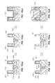
- FIG. 1( a ) and FIG. 1( b ) depict example diagrams showing a nanowire transistor, in accordance with some embodiments.
- FIG. 2 depicts an example diagram showing multiple nanowires fabricated on a substrate, in accordance with some embodiments.
- FIG. 3( a ) - FIG. 3( e ) depict example diagrams showing a process for forming a shallow-trench-isolation (STI) structure.
- STI shallow-trench-isolation
- FIG. 4( a ) - FIG. 4( f ) depict example diagrams showing a process for forming multiple nanowires after the formation of a STI structure.
- FIG. 5( a ) - FIG. 5( f ) depict other example diagrams showing a process for forming multiple nanowires on a substrate.
- FIG. 6( a ) - FIG. 6( e ) depict other example diagrams showing a process for forming a STI structure after the formation of nanowires.
- FIG. 7( a ) - FIG. 7( f ) depict example diagrams showing a process for forming a N-well and a P-well for nanowires on a substrate.
- FIG. 8 depicts an example diagram showing a N-well and a P-well formed for multiple nanowires on a substrate.
- FIG. 9( a ) - FIG. 9( f ) depict example diagrams showing a process for forming source/drain regions for nanowires.
- FIG. 10( a ) - FIG. 10( f ) depict example diagrams showing a process for forming source/drain contact regions for nanowires.
- FIG. 11( a ) - FIG. 12( f ) depict example diagrams showing a process for forming a gate dielectric material and a gate contact material for nanowires.
- FIG. 13( a ) - FIG. 13( f ) depict example diagrams showing a process for forming bottom source/drain regions for nanowires.
- FIG. 14( a ) - FIG. 14( f ) depict example diagrams showing a process for forming top source/drain regions for nanowires.
- FIG. 15( a ) - FIG. 15( f ) depict other example diagrams showing a process for forming source/drain contact regions for nanowires after the formation of bottom source/drain regions and top source/drain regions.
- FIG. 16( a ) - FIG. 17( f ) depict example diagrams showing a process for forming a gate dielectric material and a gate contact material for nanowires after the formation of source/drain contact regions.
- FIG. 18( a ) - FIG. 18( f ) depict other example diagrams showing a process for forming bottom source/drain contact regions for nanowires after the formation of bottom source/drain regions.
- FIG. 19( a ) - FIG. 19( f ) depict example diagrams showing a process for forming a gate dielectric material and a gate contact material for nanowires after the formation of bottom source/drain contact regions.
- FIG. 20( a ) - FIG. 20( f ) depict example diagrams showing a process for forming top source/drain regions for nanowires after the formation of a gate dielectric material and a gate contact material.
- FIG. 21( a ) - FIG. 21( f ) depict example diagrams showing a process for forming top source/drain contact regions for nanowires after the formation of top source/drain regions.
- FIG. 22( a ) - FIG. 22( f ) depict example diagrams showing a process for forming top metal platens for nanowires.
- FIG. 23( a ) - FIG. 23( e ) depict example diagrams showing a process for source/drain/gate contact metal formation and back-end-of-line (BEOL) interconnect formation.
- BEOL back-end-of-line
- FIG. 24 depicts an example flow chart for fabricating multiple devices on a substrate, in accordance with some embodiments.
- first and second features are formed in direct contact
- additional features may be formed between the first and second features, such that the first and second features may not be in direct contact
- present disclosure may repeat reference numerals and/or letters in the various examples. This repetition is for the purpose of simplicity and clarity and does not in itself dictate a relationship between the various embodiments and/or configurations discussed.
- spatially relative terms such as “on,” “in” and the like, may be used herein for ease of description to describe one element or feature's relationship to another element(s) or feature(s) as illustrated in the figures.
- the spatially relative terms are intended to encompass different orientations of the device in use or operation in addition to the orientation depicted in the figures.
- the apparatus may be otherwise oriented (rotated 90 degrees or at other orientations) and the spatially relative descriptors used herein may likewise be interpreted accordingly.
- FIG. 1( a ) and FIG. 1( b ) depict example diagrams showing a nanowire transistor, in accordance with some embodiments.
- a nanowire 102 is formed to fabricate a transistor 104 .
- a channel region is formed in the nanowire 102 between source/drain regions 108 .
- Spacers 110 are formed adjacent to one or more gate layers 112 on the nanowire 102 .
- Source/drain contacts 114 are formed on the source/drain regions 108 .
- a gate contact 116 is formed on the gate layers 112 that surround at least part of the nanowire 102 .
- the nanowire 102 is formed on a substrate (not shown) and is substantially vertical relative to the substrate.
- the diameter of the nanowire 102 is 6 nm. The small size of the nanowire 102 results in volume inversion of the channel 104 and thus reduces short-channel effects.
- FIG. 2 depicts an example diagram showing multiple nanowires fabricated on a substrate, in accordance with some embodiments.
- multiple nanowires 202 are fabricated on a substrate 204 and extend substantially vertically relative to the substrate 204 .
- a transistor e.g., a n-type transistor or a p-type transistor
- a transistor is fabricated using one or more vertical nanowires 202 , where a channel of the transistor is formed in the one or more vertical nanowires 202 .
- the substrate includes silicon, silicon germanium, germanium, one or more III-V materials (e.g., InP, GaAs, AlAs, InAs, InAlAs, InGaAs, InSb, GaSb, and/or InGaSb), or other suitable materials.
- the nanowires 202 include silicon, silicon germanium, germanium, one or more III-V materials (e.g., InP, GaAs, AlAs, InAs, InAlAs, InGaAs, InSb, GaSb, and/or InGaSb), or other suitable materials.
- CMOS complementary-metal-oxide-semiconductor
- FIG. 3( a ) - FIG. 3( e ) depict example diagrams showing a process for forming a shallow-trench-isolation (STI) structure.
- a mask layer 302 is formed on a substrate 304 .
- the mask layer 302 includes oxides (e.g., silicon oxide), nitrides (e.g., silicon nitride), or other suitable materials.
- the mask layer 302 is then patterned through, e.g., lithography and etching, as shown in FIG. 3( b ) .
- the thickness of the mask layer 302 is in a range of about 50 nm to about 150 nm.
- a photoresist layer 306 is formed on the mask layer 302 and exposed to a desired pattern of radiation. Then, the photoresist layer 306 is developed using a resist developer. The pattern within the photoresist layer 306 is transferred through the mask layer 302 and into the underlying substrate 304 . A single etch (e.g., dry etch or wet etch) or multiple etching can be used for transferring the pattern through the mask layer 302 and into the underlying substrate 304 .
- a dielectric material 310 e.g., oxides
- the depth of the gap 308 is in a range of about 120 nm to about 400 nm.
- a chemical-mechanical planarization/polishing (CMP) process is carried out to remove part of the dielectric material 310 and stops at the mask layer 302 , as shown in FIG. 3( d ) .
- the dielectric material 310 e.g., oxides
- etching e.g., dry etching
- the thickness of the STI structure 312 is in a range of about 20 nm to about 350 nm.
- the mask layer 302 and the dielectric material 310 are formed through chemical vapor deposition (CVD), plasma enhanced chemical vapor deposition (PECVD), physical vapor deposition (PVD), sputtering, atomic layer deposition (ALD), or other suitable processes.
- CVD chemical vapor deposition
- PECVD plasma enhanced chemical vapor deposition
- PVD physical vapor deposition
- ALD atomic layer deposition
- FIG. 4( a ) - FIG. 4( f ) depict example diagrams showing a process for forming multiple nanowires after the formation of the STI structure 312 .
- a bottom-anti-reflective-coating (BARC) layer 402 is formed on the mask layer 302 and the STI structure 312 .
- a photoresist layer 404 is formed on the BARC layer 402 , and exposed to a desired pattern of radiation. Then, the photoresist layer 404 is developed using a resist developer to expose part of the BARC layer 402 , as shown in FIG. 4( b ) .
- the exposed BARC layer 402 , part of the mask layer 302 and part of the substrate 304 that are under the exposed BARC layer 402 are removed through, e.g., etching (e.g., dry etching or wet etching), as shown in FIG. 4( c ) .
- the remaining BARC layer 402 and the remaining photoresist layer 404 are removed, as shown in FIG. 4( d ) .
- An annealing process is carried out for nanowires 406 and 408 , as shown in FIG. 4( e ) .
- the heights of the nanowires 406 and 408 are in a range of about 20 nm to about 100 nm.
- the annealing process is performed in hydrogen (e.g., with a pressure in a range of about 7 torr to about 600 torr) at a temperature in a range of about 600° C. to about 1000° C.
- the nanowires 406 and 408 may be smoothed during the annealing process to become, e.g., elliptical shaped or cylindrical shaped.
- the nanowires 406 and 408 are separated by the STI structure 312 and extend substantially vertically relative to the substrate 304 .
- a top surface of the STI structure 312 is at approximately a same level of a top surface of the substrate 304 after the nanowires 406 and 408 are formed.
- the top surface of the STI structure 312 is higher than the top surface of the substrate 304 (not shown in FIG. 4( e ) ) for about 1 nm to about 25 nm after the nanowires 406 and 408 are formed.
- the top surface of the STI structure 312 is lower than the top surface of the substrate 304 (not shown in FIG.
- nanowires 406 and 408 are oxidized partially and the formed oxides are stripped (e.g., through etching) to thin down the nanowires 406 and 408 .
- the diameters of the stripped nanowires 406 and 408 are in a range of about 4 nm to about 10 nm.
- a forest of nanowires may be formed on the substrate 304 according to the processes described above, as shown in FIG. 4( f ) .
- FIG. 5( a ) - FIG. 5( f ) depict other example diagrams showing a process for forming multiple nanowires on a substrate.
- a mask layer 502 is formed on a substrate 504 .
- the mask layer 502 includes oxides (e.g., silicon oxide), nitrides (e.g., silicon nitride), or other suitable materials.
- the thickness of the mask layer 502 is in a range of about 50 nm to about 150 nm.
- the mask layer 502 is then patterned using a photoresist layer 506 , part of the mask layer 502 is removed (e.g., through etching) to expose the substrate 504 , as shown in FIG.
- the mask layer 502 is etched through reactive ion etching (RIE).
- RIE reactive ion etching
- the photoresist layer 506 is removed, and part of the exposed substrate 504 is etched (e.g., through dry etching) to form nanowires 508 and 510 , as shown in FIG. 5( c ) .
- the nanowires 508 and 510 extend substantially vertically relative to the substrate 504 .
- An annealing process (e.g., in hydrogen) is carried out for the nanowires 508 and 510 , as shown in FIG. 5( d ) .
- a dielectric material 512 e.g., oxides
- a CMP process is carried out to remove part of the dielectric material 512 and stops at the mask layer 502 , as shown in FIG. 5( f ) .
- FIG. 6( a ) - FIG. 6( e ) depict other example diagrams showing a process for forming a STI structure after the formation of the nanowires 508 and 510 .
- a photoresist layer 602 is formed on wafer and exposed to a desired pattern of radiation. Then, the photoresist layer 602 is developed using a resist developer. The pattern within the photoresist layer 602 is transferred through the dielectric material 512 and into the underlying substrate 504 .
- a single etch e.g., dry etch or wet etch
- multiple etching can be used for transferring the pattern to form a gap 604 .
- the depth of the gap 604 is in a range of about 120 nm to about 400 nm.
- Another dielectric material 606 e.g., oxides
- a CMP process is carried out to remove part of the dielectric material 606 and stops at the mask layer 502 , as shown in FIG. 6( c ) .
- the dielectric material 606 (e.g., oxides) is further removed through etching (e.g., dry etching) to form the STI structure 608 , as shown in FIG. 6( d ) .
- the nanowires 508 and 510 are separated by the STI structure 608 and extend substantially vertically relative to the substrate 504 .
- a top surface of the STI structure 608 is at approximately a same level of a top surface of the substrate 504 after the nanowires 508 and 510 are formed.
- the top surface of the STI structure 608 is higher than the top surface of the substrate 504 (not shown in FIG. 6( d ) ) for about 1 nm to about 25 nm after the nanowires 508 and 510 are formed.
- the top surface of the STI structure 608 is lower than the top surface of the substrate 504 (not shown in FIG. 6( d ) ) for about 2 nm to about 25 nm after the nanowires 508 and 510 are formed.
- a forest of nanowires may be formed on the substrate 504 according to the processes described above, as shown in FIG. 6( e ) .
- the thickness of the STI structure 608 is in a range of about 20 nm to about 350 nm.
- the heights of the nanowires 508 and 510 are in a range of about 20 nm to about 100 nm.
- FIG. 7( a ) - FIG. 7( f ) depict example diagrams showing a process for forming a N-well and a P-well for nanowires on a substrate.
- nanowires 702 and 704 e.g., nanowires 406 and 408 , or nanowires 508 and 510
- a STI structure 708 is formed between the nanowires 702 and 704 .
- a BARC layer 710 is formed on the wafer. In some embodiments, part of the BARC layer 710 is removed, e.g., through etching or CMP.
- a photoresist layer 712 is formed on the BARC layer 710 , and part of the photoresist layer 712 is removed through lithography, as shown in FIG. 7( a ) .
- part of the BARC layer 710 is removed, e.g., through etching. Ion implantation is performed to form a N-well 714 for the nanowire 702 .
- a hard-mask material 716 protects the nanowire 702 from the ion implantation.
- the remaining photoresist layer 712 and the remaining BARC layer 710 are removed, as shown in FIG. 7( c ) .
- an annealing process is carried out for annealing the formed N-well 714 .
- another BARC layer 718 is formed on the wafer.
- part of the BARC layer 718 is removed, e.g., through etching or CMP.
- a photoresist layer 720 is formed on the BARC layer 718 , and part of the photoresist layer 720 is removed through lithography, as shown in FIG. 7( d ) .
- Part of the BARC layer 718 is removed, e.g., through etching, and ion implantation is performed to form a P-well 722 for the nanowire 704 , as shown in FIG. 7( e ) .
- a hard-mask material 724 protects the nanowire 704 from the ion implantation.
- the remaining photoresist layer 720 and the remaining BARC layer 718 are removed, as shown in FIG. 7( f ) .
- An annealing process is carried out for annealing the N-well 714 and the P-well 722 .
- the formation of a N-well and a P-well may be performed for a forest of nanowires on a substrate according to the processes described above, as shown in FIG. 8 .
- FIG. 9( a ) - FIG. 9( f ) depict example diagrams showing a process for forming source/drain regions for the nanowires 702 and 704 .
- a BARC layer 802 is formed on the wafer, and a photoresist layer 804 is formed on the BARC layer 802 .
- Part of the BARC layer 802 and part of the photoresist layer 804 are removed.
- Ion implantation is performed (e.g., along a direction perpendicular to the substrate 706 ) to form n-doped source/drain regions 806 and 808 for the nanowire 704 .
- a height associated with the source/drain region 806 is greater than that of the source/drain region 808 , relative to the substrate 706 .
- an annealing process is carried out for the formed source/drain regions 806 and 808 .
- ion implantation is carried out (e.g., along a direction not perpendicular to the substrate 706 ) to form a doped channel region 810 in the nanowire 704 , as shown in FIG. 9( b ) .
- the channel region 810 is n-doped for fabricating an accumulation-mode transistor.
- the channel region 810 is p-doped for fabricating an inversion-mode transistor.
- an annealing process is performed for the channel region 810 .
- the remaining BARC layer 802 and the remaining photoresist layer 804 are removed.
- Another BARC layer 812 is formed on the wafer, and a photoresist layer 814 is formed on the BARC layer 812 , as shown in FIG. 9( d ) .
- Part of the BARC layer 812 and part of the photoresist layer 814 are removed.
- Ion implantation is performed (e.g., along a direction perpendicular to the substrate 706 ) to form p-doped source/drain regions 816 and 818 for the nanowire 702 .
- a height associated with the source/drain region 816 is greater than that of the source/drain region 818 , relative to the substrate 706 .
- an annealing process is carried out for the formed source/drain regions 816 and 818 .
- ion implantation is carried out (e.g., along a direction not perpendicular to the substrate 706 ) to form a doped channel region 820 in the nanowire 702 , as shown in FIG. 9( e ) .
- the channel region 820 is p-doped for fabricating an accumulation-mode transistor.
- the channel region 820 is n-doped for fabricating an inversion-mode transistor.
- an annealing process is performed for the channel region 820 .
- the remaining BARC layer 812 and the remaining photoresist layer 814 are removed.
- An annealing process is performed for the formed source/drain regions and/or the channel regions.
- FIG. 10( a ) - FIG. 10( f ) depict example diagrams showing a process for forming source/drain contact regions for the nanowires 702 and 704 .
- a spacer material 902 e.g., silicon nitride
- the thickness of the spacer material 902 is in a range of about 1 ⁇ 2 to about 3 times of the diameter of the nanowires 702 and 704 .
- Part of the spacer material 902 is removed, e.g., through etching, as shown in FIG. 10( b ) .
- the width of the remaining spacer material 902 adjacent to the nanowires 702 and 704 is in a range of about 1 ⁇ 3 to about 2 times of the diameter of the nanowires 702 and 704 .
- a material layer 904 including a metal-containing material (e.g., Ti, Ni(Pt)) and a cap layer (e.g., TiN) is formed on the wafer, as shown in FIG. 10( c ) .
- the thickness of 904 is about 1 ⁇ 4 to about 1 ⁇ 2 of the depths of the source/drain regions 818 and 808 for the nanowires 702 and 704 respectively.
- An annealing process is performed to form source/drain contact regions 906 associated with the nanowire 702 and source/drain contact regions 908 associated with the nanowire 704 , as shown in FIG. 10( d ) .
- the contact regions 906 e.g., silicides
- the contact regions 908 are formed through salicidation of the material layer 904 and the source/drain regions 806 and 808 .
- the un-reacted material layer 904 is removed, e.g., through wet etching. As shown in FIG.
- the remaining spacer material 902 is removed, e.g., through etching.
- a contact-etch-stop layer (CESL) 910 and a dielectric material 912 (e.g., oxides) are formed on the wafer, as shown in FIG. 10( f ) .
- the top surface of the STI structure 708 is about at the same level of the top surface of the contact regions 906 and 908 adjacent to the STI structure 708 . In some embodiments, the top surface of the STI structure 708 is higher than the top surface of the contact regions 906 and 908 adjacent to the STI structure 708 about 10 angstroms to about 250 angstroms.
- the top surface of the STI structure 708 is lower than the top surface of the contact regions 906 and 908 adjacent to the STI structure 708 about 2 nm to about 45 nm. (Note to agent: similar thickness range applies to the rest of embodiments.)
- FIG. 11( a ) - FIG. 12( f ) depict example diagrams showing a process for forming a gate dielectric material and a gate contact material for the nanowires 702 and 704 .
- a CMP process is performed to remove part of the dielectric material 912 and stops at the CESL 910 .
- Part of the dielectric material 912 and part of the CESL 910 are removed, e.g., through dry etching, as shown in FIG. 11( b ) .
- the thickness of the remaining dielectric material 912 over the source/drain regions or the STI structure is about 1 ⁇ 4 to about 1 ⁇ 2 of the heights of the nanowires 702 and 704 .
- a gate dielectric material 1002 including an interfacial layer and a high-k dielectric material is formed on the wafer, and a p-type-work-function metal material 1004 is formed on the gate dielectric material 1002 , as shown in FIG. 11( c ) .
- the high-k dielectric material includes HfO 2 , ZrO 2 , La 2 O 3 , Al 2 O 3 , TiO 2 , SrTiO 3 , LaAlO 3 , Y 2 O 3 , HfO x N y , ZrO x N y , La 2 O x N y , Al 2 O x N y , TiO x N y , or other suitable materials.
- the p-type-work-function-metal material 1004 includes titanium-nitride-containing materials, aluminum-containing materials, or other suitable materials.
- a BARC layer 1006 and a photoresist layer 1008 are formed on the wafer, and part of the BARC layer 1006 and part of the photoresist layer 1008 are removed to expose part of the p-type-work-function-metal material 1004 .
- the exposed p-type-work-function-metal material 1004 is removed, e.g., through etching.
- the remaining BARC layer 1006 and the remaining photoresist layer 1008 are removed.
- a n-type-work-function-metal material 1010 is formed on the wafer, as shown in FIG. 11( e ) .
- the n-type-work-function-metal material 1010 includes titanium-nitride-containing materials, lanthanum-containing materials, or other suitable materials.
- a gate contact material 1012 is formed on the n-type-work-function-metal material 1010 , as shown in FIG. 11( f ) .
- the gate contact material 1012 includes aluminum, tungsten, cobalt, copper, or other suitable materials.
- a CMP process is carried out to remove part of the gate contact material 1012 and stops at the n-type-work-function-metal material 1010 .
- Part of the gate contact material 1012 and part of the n-type-work-function-metal material 1010 are removed, e.g., through etching, as shown in FIG. 12( b ) .
- a BARC layer 1102 is formed on the wafer, and a photoresist layer 1104 is formed on the BARC layer 1102 .
- the photoresist layer 1104 is patterned through lithography to expose part of the BARC layer 1102 .
- the exposed BARC layer 1102 , part of the gate contact material 1012 , part of the n-type-work-function-metal material 1010 , and part of the gate dielectric material 1002 are removed, e.g., through etching, as shown in FIG. 12( d ) .
- the remaining BARC layer 1102 and the remaining photoresist layer 1104 are removed, as shown in FIG. 12( e ) .
- a dielectric material 1106 is formed on the wafer, as shown in FIG. 12( f ) .
- a CMP process is performed to remove part of the dielectric material 1106 and stops at top surfaces of the nanowires 702 and 704 .
- FIG. 13( a ) - FIG. 13( f ) depict example diagrams showing a process for forming bottom source/drain regions for the nanowires 702 and 704 .
- a BARC layer 1202 is formed on the wafer, and a photoresist layer 1204 is formed on the BARC layer 1202 . Part of the BARC layer 1202 and part of the photoresist layer 1204 are removed.
- Ion implantation is performed (e.g., along a direction perpendicular to the substrate 706 ) to form a n-doped source/drain region 1206 in contact with a bottom part of the nanowire 704 .
- the hard-mask material 724 protects a top part of the nanowire 704 from the ion implantation.
- an annealing process is carried out for the formed source/drain region 1206 .
- ion implantation is carried out (e.g., along a direction not perpendicular to the substrate 706 ) to form a doped channel region 1210 in the nanowire 704 , as shown in FIG. 13( b ) .
- the channel region 1210 is n-doped for fabricating an accumulation-mode transistor.
- the channel region 1210 is p-doped for fabricating an inversion-mode transistor.
- an annealing process is performed for the channel region 1210 .
- the remaining BARC layer 1202 and the remaining photoresist layer 1204 are removed.
- Another BARC layer 1212 is formed on the wafer, and a photoresist layer 1214 is formed on the BARC layer 1212 , as shown in FIG. 13( d ) .
- Part of the BARC layer 1212 and part of the photoresist layer 1214 are removed.
- Ion implantation is performed (e.g., along a direction perpendicular to the substrate 706 ) to form a p-doped source/drain region 1216 in contact with a bottom part of the nanowire 702 .
- the hard-mask material 716 protects a top part of the nanowire 702 from the ion implantation.
- an annealing process is carried out for the formed source/drain region 1216 .
- ion implantation is carried out (e.g., along a direction not perpendicular to the substrate 706 ) to form a doped channel region 1220 in the nanowire 702 , as shown in FIG. 13( e ) .
- the channel region 1220 is p-doped for fabricating an accumulation-mode transistor.
- the channel region 1220 is n-doped for fabricating an inversion-mode transistor.
- an annealing process is performed for the channel region 1220 .
- the remaining BARC layer 1212 and the remaining photoresist layer 1214 are removed.
- An annealing process is performed for the formed source/drain regions 1206 and 1216 and/or the channel regions 1210 and 1220 .
- FIG. 14( a ) - FIG. 14( f ) depict example diagrams showing a process for forming top source/drain regions for the nanowires 702 and 704 .
- a dielectric material 1302 e.g., oxides
- a CMP process is performed to remove part of the dielectric material 1302 and stops at the hard-mask materials 716 and 724 .
- the hard-mask materials 716 and 724 are removed, e.g., through etching.
- a photoresist layer 1304 is formed on the wafer and part of the photo resist layer 1304 is removed to expose the nanowire 704 . Ion implantation is performed (e.g., along a direction perpendicular to the substrate 706 ) to form a n-doped source/drain region 1306 in a top part of the nanowire 704 . The remaining photoresist layer 1304 is removed.
- another photoresist layer 1308 is formed on the wafer and part of the photo resist layer 1308 is removed to expose the nanowire 702 .
- Ion implantation is performed (e.g., along a direction perpendicular to the substrate 706 ) to form a p-doped source/drain region 1310 in a top part of the nanowire 702 .
- the remaining photoresist layer 1308 is removed, as shown in FIG. 14( e ) .
- a high-temperature annealing process is performed to activate dopants in the source/drain regions 1206 , 1216 , 1306 and 1310 .
- the dielectric material 1302 is removed, e.g., through etching, as shown in FIG. 14( f ) .
- FIG. 15( a ) - FIG. 15( f ) depict other example diagrams showing a process for forming source/drain contact regions for the nanowires 702 and 704 after the formation of the bottom source/drain regions and the top source/drain regions.
- a spacer material 1402 e.g., silicon nitride
- the thickness of the spacer material 902 is in a range of about 1 ⁇ 2 to about 3 times of the diameter of the nanowires 702 and 704 .
- Part of the spacer material 1402 is removed, e.g., through etching, as shown in FIG. 15( b ) .
- the width of the remaining spacer material 1402 adjacent to the nanowires 702 and 704 is in a range of about 1 ⁇ 3 to about 2 times of the diameter of the nanowires 702 and 704 .
- a material layer 1404 including a metal-containing material (e.g., Ti, Ni(Pt)) and a cap layer (e.g., TiN) is formed on the wafer, as shown in FIG. 15( c ) .
- the thickness of 1404 is about 1 ⁇ 4 to about 1 ⁇ 2 of the depths of the source/drain regions 818 and 808 for the nanowires 702 and 704 respectively.
- An annealing process is performed to form source/drain contact regions 1406 and 1408 associated with the nanowire 702 and form source/drain contact regions 1410 and 1412 associated with the nanowire 704 , as shown in FIG. 15( d ) .
- the contact regions 1406 and 1408 e.g., silicides
- the contact regions 1410 and 1412 are formed through salicidation of the material layer 1404 and the source/drain regions 1306 and 1206 , respectively.
- the un-reacted material layer 1404 is removed, e.g., through wet etching. As shown in FIG.
- the remaining spacer material 1402 is removed, e.g., through etching.
- a contact-etch-stop layer (CESL) 1510 and a dielectric material 1512 (e.g., oxides) are formed on the wafer, as shown in FIG. 15( f ) .
- the top surface of the STI structure is at about the same level of the top surface of the contact regions 1408 and 1412 adjacent to the STI structure. In some embodiments, the top surface of the STI structure is higher than the top surface of the contact regions 1408 and 1412 adjacent to the STI structure for about 1 nm to about 25 nm. In some embodiments, the top surface of the STI structure is lower than the top surface of the contact regions 1408 and 1412 adjacent to the STI structure for about 2 nm to about 45 nm.
- FIG. 16( a ) - FIG. 17( f ) depict example diagrams showing a process for forming a gate dielectric material and a gate contact material for the nanowires 702 and 704 after the formation of the source/drain contact regions.
- the process shown in FIG. 16( a ) - FIG. 17( f ) is similar to the process shown in FIG. 11( a ) - FIG. 12( f ) .
- FIG. 18( a ) - FIG. 18( f ) depict other example diagrams showing a process for forming bottom source/drain contact regions for the nanowires 702 and 704 after the formation of the bottom source/drain regions.
- a spacer material 1802 e.g., silicon nitride
- An annealing process is performed to form a bottom source/drain contact region 1806 associated with the nanowire 702 and form a bottom source/drain contact region 1808 associated with the nanowire 704 , as shown in FIG. 18( c ) .
- the contact regions 1806 and 1808 e.g., silicides
- the un-reacted material layer 1804 is removed, e.g., through wet etching.
- the remaining spacer material 1802 is removed and the hard-mask materials 716 and 724 are removed, e.g., through etching.
- a contact-etch-stop layer (CESL) 1810 and a dielectric material 1812 are formed on the wafer, as shown in FIG. 18( e ) .
- a CMP process is performed to remove part of the dielectric material 1812 and stops at the CESL 1810 , as shown in FIG. 18( f ) .
- FIG. 19( a ) - FIG. 19( f ) depict example diagrams showing a process for forming a gate dielectric material and a gate contact material for the nanowires 702 and 704 after the formation of the bottom source/drain contact regions.
- part of the dielectric material 1812 and part of the CESL 1810 are removed, e.g., through dry etching.
- the thickness of the remaining dielectric material 1812 over the source/drain regions or the STI structure is about 1 ⁇ 4 to about 1 ⁇ 2 of the heights of the nanowires 702 and 704 .
- a gate dielectric material 1902 including an interfacial layer and a high-k dielectric material is formed on the wafer, and a p-type-work-function metal material 1904 is formed on the gate dielectric material 1902 , as shown in FIG. 19( b ) .
- a BARC layer 1906 and a photoresist layer 1908 are formed on the wafer, and part of the BARC layer 1906 and part of the photoresist layer 1908 are removed to expose part of the p-type-work-function-metal material 1904 .
- the exposed p-type-work-function-metal material 1904 is removed, e.g., through etching.
- a n-type-work-function-metal material 1910 is formed on the wafer, as shown in FIG. 19( d ) .
- a gate contact material 1912 is formed on the n-type-work-function-metal material 1910 , as shown in FIG. 19( e ) .
- the gate contact material 1912 includes aluminum, tungsten, cobalt, copper, or other suitable materials.
- a CMP process is carried out to remove part of the gate contact material 1912 and stops at the n-type-work-function-metal material 1910 .
- FIG. 20( a ) - FIG. 20( f ) depict example diagrams showing a process for forming top source/drain regions for the nanowires 702 and 704 after the formation of the gate dielectric material 1902 and the gate contact material 1912 .
- part of the gate contact material 1912 and part of the n-type-work-function-metal material 1910 are removed, e.g., through etching, as shown in FIG. 20( a ) .
- a dielectric material 2002 is formed on the wafer.
- a CMP process is performed to remove part of the dielectric material 2002 and stops at the top surfaces of the nanowires 702 and 704 , as shown in FIG. 20( c ) .
- a photoresist layer 2004 is formed on the wafer, and part of the photoresist layer 2004 is removed to expose a top part of the nanowire 704 , as shown in FIG. 20( d ) .
- Ion implantation is performed (e.g., along a direction perpendicular to the substrate 706 ) to form a n-doped source/drain region 2006 in a top part of the nanowire 704 .
- the remaining photoresist layer 2004 is removed.
- another photoresist layer 2008 is formed on the wafer and part of the photo resist layer 2008 is removed to expose the nanowire 702 .
- Ion implantation is performed (e.g., along a direction perpendicular to the substrate 706 ) to form a p-doped source/drain region 2010 in a top part of the nanowire 702 .
- the remaining photoresist layer 2008 is removed, as shown in FIG. 20( f ) .
- a high-temperature annealing process is performed to activate dopants in the source/drain regions 1206 , 1216 , 2006 and 2010 .
- FIG. 21( a ) - FIG. 21( f ) depict example diagrams showing a process for forming top source/drain contact regions for the nanowires 702 and 704 after the formation of the top source/drain regions.
- a photoresist layer 2102 is formed on the wafer, and part of the photoresist 2102 is removed to expose part of the dielectric material 2002 .
- the exposed dielectric material 2002 , part of the gate contact material 1912 , part of the n-type-work-function-metal material 1910 , and part of the gate dielectric material 1902 are removed, e.g., through etching.
- the remaining photoresist layer 2102 is removed, as shown in FIG.
- a dielectric material 2104 (e.g., oxides) is formed on the wafer, as shown in FIG. 21( c ) .
- a CMP process is performed to remove part of the dielectric material 2104 and stops at top surfaces of the nanowires 702 and 704 , as shown in FIG. 21( d ) .
- a material layer 2106 including a metal-containing material (e.g., Ti, Ni(Pt)) and a cap layer (e.g., TiN) is formed on the wafer, as shown in FIG. 21( e ) .
- An annealing process is performed to form a top source/drain contact region 2108 associated with the nanowire 702 and form a top source/drain contact region 2110 associated with the nanowire 704 , as shown in FIG. 21( f ) .
- the contact regions 2108 and 2110 e.g., silicides
- the un-reacted material layer 2106 is removed, e.g., through wet etching.
- FIG. 22( a ) - FIG. 22( f ) depict example diagrams showing a process for forming top metal platens for the nanowires 702 and 704 .
- a top metal material 2202 is formed on the wafer.
- the top metal material 2202 includes titanium, titanium nitride, tungsten, aluminum, cobalt, copper, or other suitable materials.
- a photoresist layer 2204 is formed and part of the photoresist layer 2204 is removed to expose part of the top metal material 2202 .
- the exposed top metal material 2202 is removed, e.g., through dry etching, as shown in FIG. 22( b ) .
- the remaining photoresist layer 2204 is removed, as shown in FIG. 22( c ) .
- An inter-layer-dielectric (ILD) layer 2206 (e.g., oxides) is formed on the wafer, as shown in FIG. 22( d ) .
- a CMP process is performed to remove part of the ILD layer 2206 , as shown in FIG. 22( e ) .
- Another photoresist layer 2208 is formed on the ILD layer 2206 , and patterned through lithography for source/drain/gate contact metal formation, as shown in FIG. 22( f ) .
- FIG. 23( a ) - FIG. 23( e ) depict example diagrams showing a process for source/drain/gate contact metal formation and back-end-of-line (BEOL) interconnect formation.
- the patterned photoresist layer 2208 is used as a mask for removing part of the ILD layer 2206 .
- the remaining photoresist layer 2008 is removed, as shown in FIG. 23( b ) .
- One or more contact metal materials 2302 e.g., Ti/TiN/W
- a CMP process is performed to remove part of the contact metal materials 2302 to form source/drain/gate contact structures, as shown in FIG.
- Interconnect structures 2304 are formed during one or more BEOL interconnect processes, as shown in FIG. 23( e ) .
- the thickness of the CESL is about 1 ⁇ 4 to about 4 times of the diameter of the nanowire 702 .
- the thickness of the CESL 1810 is in a range of about 2 nm to about 20 nm as a buffer layer for removing part of the ILD layer 2206 , e.g., through etching.
- FIG. 24 depicts an example flow chart for fabricating multiple devices on a substrate, in accordance with some embodiments.
- a first nanowire e.g., the nanowire 704
- a second nanowire e.g., the nanowire 702
- the first nanowire and the second nanowire extending substantially vertically relative to the substrate.
- a first source region e.g., the source/drain region 806 or 808 , the source/drain region 1206 or 1306
- a first drain region e.g., the source/drain region 806 or 808 , the source/drain region 1206 or 1306
- a second source region e.g., the source/drain region 816 or 818 , the source/drain region 1216 or 1310
- a second drain region e.g., the source/drain region 816 or 818 , the source/drain region 1216 or 1310
- the second nanowire being disposed between the second source region and the second drain region.
- the present disclosure describes vertical gate-all-around nanowire arrays (e.g., with salicided source/drain contact regions, scaled high-k dielectric materials and metal gate structures) fabricated using processes compatible with a CMOS process flow.
- the structures, devices and methods described herein are configured to reduce short channel effects, reduce device-to-device variability and achieve nanometer-gate-length patterning without high-resolution lithography.
- a method for fabricating nanowire devices on a substrate.
- a first nanowire and a second nanowire are formed on a substrate, the first nanowire and the second nanowire extending substantially vertically relative to the substrate.
- a first source region and a first drain region are formed with n-type dopants, the first nanowire being disposed between the first source region and the first drain region.
- a second source region and a second drain region are formed with p-type dopants, the second nanowire being disposed between the second source region and the second drain region.
- a structure includes: a first nanowire, a first source region, a first drain region, a second nanowire, a second source region, and a second drain region.
- the first nanowire is formed on a substrate and extends substantially vertically relative to the substrate.
- the first source region includes first n-type dopants, and the first drain region includes second n-type dopants.
- the first nanowire is disposed between the first source region and the first drain region.
- the second nanowire is formed on the substrate and extends substantially vertically relative to the substrate.
- the second source region includes first p-type dopants, and the second drain region includes second p-type dopants.
- the second nanowire is disposed between the second source region and the second drain region.
- a device includes a n-type transistor and a p-type transistor.
- the n-type transistor includes: a first source region in contact with a first end of one or more first nanowires formed on a substrate, the first end being associated with a first height relative to the substrate; a first drain region in contact with a second end of the first nanowires, the second end being associated with a second height relative to the substrate, the second height being different from the first height; and a first channel region in the first nanowires configured to conduct a first current between the first source region and the first drain region.
- the p-type transistor includes: a second source region in contact with a third end of one or more second nanowires formed on the substrate, the third end being associated with a third height relative to the substrate; a second drain region in contact with a fourth end of the second nanowires, the fourth end being associated with a fourth height relative to the substrate, the fourth height being different from the third height; and a second channel region in the second nanowires configured to conduct a second current between the second source region and the second drain region.
Abstract
Systems and methods are provided for fabricating nanowire devices on a substrate. A first nanowire and a second nanowire are formed on a substrate, the first nanowire and the second nanowire extending substantially vertically relative to the substrate. A first source region and a first drain region are formed with n-type dopants, the first nanowire being disposed between the first source region and the first drain region. A second source region and a second drain region are formed with p-type dopants, the second nanowire being disposed between the second source region and the second drain region.
Description
The technology described in this disclosure relates generally to semiconductor devices and more particularly to fabrication of semiconductor devices.
As feature sizes of semiconductor devices continue to shrink (e.g., into a sub 50 nm regime), various problems, such as short-channel effects and poor sub-threshold characteristics, often become severe in traditional planar devices. Novel device geometries with enhanced performance are needed to push toward higher packing densities in devices and circuits.
Aspects of the present disclosure are best understood from the following detailed description when read with the accompanying figures. It is noted that, in accordance with the standard practice in the industry, various features are not drawn to scale. In fact, the dimensions of the various features may be arbitrarily increased or reduced for clarity of discussion.
The following disclosure provides many different embodiments, or examples, for implementing different features of the invention. Specific examples of components and arrangements are described below to simplify the present disclosure. These are, of course, merely examples and are not intended to be limiting. For example, the formation of a first feature over or on a second feature in the description that follows may include embodiments in which the first and second features are formed in direct contact, and may also include embodiments in which additional features may be formed between the first and second features, such that the first and second features may not be in direct contact. In addition, the present disclosure may repeat reference numerals and/or letters in the various examples. This repetition is for the purpose of simplicity and clarity and does not in itself dictate a relationship between the various embodiments and/or configurations discussed.
Further, spatially relative terms, such as “on,” “in” and the like, may be used herein for ease of description to describe one element or feature's relationship to another element(s) or feature(s) as illustrated in the figures. The spatially relative terms are intended to encompass different orientations of the device in use or operation in addition to the orientation depicted in the figures. The apparatus may be otherwise oriented (rotated 90 degrees or at other orientations) and the spatially relative descriptors used herein may likewise be interpreted accordingly.
As shown in FIG. 4(e) , the nanowires 406 and 408 are separated by the STI structure 312 and extend substantially vertically relative to the substrate 304. A top surface of the STI structure 312 is at approximately a same level of a top surface of the substrate 304 after the nanowires 406 and 408 are formed. In some embodiments, the top surface of the STI structure 312 is higher than the top surface of the substrate 304 (not shown in FIG. 4(e) ) for about 1 nm to about 25 nm after the nanowires 406 and 408 are formed. In certain embodiments, the top surface of the STI structure 312 is lower than the top surface of the substrate 304 (not shown in FIG. 4(e) ) for about 2 nm to about 25 nm after the nanowires 406 and 408 are formed. In some embodiments, the nanowires 406 and 408 are oxidized partially and the formed oxides are stripped (e.g., through etching) to thin down the nanowires 406 and 408. The diameters of the stripped nanowires 406 and 408 are in a range of about 4 nm to about 10 nm. A forest of nanowires may be formed on the substrate 304 according to the processes described above, as shown in FIG. 4(f) .
The dielectric material 606 (e.g., oxides) is further removed through etching (e.g., dry etching) to form the STI structure 608, as shown in FIG. 6(d) . The nanowires 508 and 510 are separated by the STI structure 608 and extend substantially vertically relative to the substrate 504. A top surface of the STI structure 608 is at approximately a same level of a top surface of the substrate 504 after the nanowires 508 and 510 are formed. In some embodiments, the top surface of the STI structure 608 is higher than the top surface of the substrate 504 (not shown in FIG. 6(d) ) for about 1 nm to about 25 nm after the nanowires 508 and 510 are formed. In certain embodiments, the top surface of the STI structure 608 is lower than the top surface of the substrate 504 (not shown in FIG. 6(d) ) for about 2 nm to about 25 nm after the nanowires 508 and 510 are formed. A forest of nanowires may be formed on the substrate 504 according to the processes described above, as shown in FIG. 6(e) . For example, the thickness of the STI structure 608 is in a range of about 20 nm to about 350 nm. The heights of the nanowires 508 and 510 are in a range of about 20 nm to about 100 nm.
As shown in FIG. 7(b) , part of the BARC layer 710 is removed, e.g., through etching. Ion implantation is performed to form a N-well 714 for the nanowire 702. A hard-mask material 716 protects the nanowire 702 from the ion implantation. The remaining photoresist layer 712 and the remaining BARC layer 710 are removed, as shown in FIG. 7(c) . In certain embodiments, an annealing process is carried out for annealing the formed N-well 714.
As shown in FIG. 7(d) , another BARC layer 718 is formed on the wafer. In some embodiments, part of the BARC layer 718 is removed, e.g., through etching or CMP. A photoresist layer 720 is formed on the BARC layer 718, and part of the photoresist layer 720 is removed through lithography, as shown in FIG. 7(d) . Part of the BARC layer 718 is removed, e.g., through etching, and ion implantation is performed to form a P-well 722 for the nanowire 704, as shown in FIG. 7(e) . A hard-mask material 724 protects the nanowire 704 from the ion implantation. The remaining photoresist layer 720 and the remaining BARC layer 718 are removed, as shown in FIG. 7(f) . An annealing process is carried out for annealing the N-well 714 and the P-well 722. The formation of a N-well and a P-well may be performed for a forest of nanowires on a substrate according to the processes described above, as shown in FIG. 8 .
In some embodiments, ion implantation is carried out (e.g., along a direction not perpendicular to the substrate 706) to form a doped channel region 810 in the nanowire 704, as shown in FIG. 9(b) . For example, the channel region 810 is n-doped for fabricating an accumulation-mode transistor. In another example, the channel region 810 is p-doped for fabricating an inversion-mode transistor. After ion implantation, an annealing process is performed for the channel region 810.
As shown in FIG. 9(c) , the remaining BARC layer 802 and the remaining photoresist layer 804 are removed. Another BARC layer 812 is formed on the wafer, and a photoresist layer 814 is formed on the BARC layer 812, as shown in FIG. 9(d) . Part of the BARC layer 812 and part of the photoresist layer 814 are removed. Ion implantation is performed (e.g., along a direction perpendicular to the substrate 706) to form p-doped source/ drain regions 816 and 818 for the nanowire 702. For example, a height associated with the source/drain region 816 is greater than that of the source/drain region 818, relative to the substrate 706. In some embodiments, an annealing process is carried out for the formed source/ drain regions 816 and 818.
In certain embodiments, ion implantation is carried out (e.g., along a direction not perpendicular to the substrate 706) to form a doped channel region 820 in the nanowire 702, as shown in FIG. 9(e) . For example, the channel region 820 is p-doped for fabricating an accumulation-mode transistor. In another example, the channel region 820 is n-doped for fabricating an inversion-mode transistor. After ion implantation, an annealing process is performed for the channel region 820. As shown in FIG. 9(f) , the remaining BARC layer 812 and the remaining photoresist layer 814 are removed. An annealing process is performed for the formed source/drain regions and/or the channel regions.
As shown in FIG. 11(d) , a BARC layer 1006 and a photoresist layer 1008 are formed on the wafer, and part of the BARC layer 1006 and part of the photoresist layer 1008 are removed to expose part of the p-type-work-function-metal material 1004. The exposed p-type-work-function-metal material 1004 is removed, e.g., through etching. The remaining BARC layer 1006 and the remaining photoresist layer 1008 are removed. A n-type-work-function-metal material 1010 is formed on the wafer, as shown in FIG. 11(e) . For example, the n-type-work-function-metal material 1010 includes titanium-nitride-containing materials, lanthanum-containing materials, or other suitable materials. A gate contact material 1012 is formed on the n-type-work-function-metal material 1010, as shown in FIG. 11(f) . For example, the gate contact material 1012 includes aluminum, tungsten, cobalt, copper, or other suitable materials.
As shown in FIG. 12(a) , a CMP process is carried out to remove part of the gate contact material 1012 and stops at the n-type-work-function-metal material 1010. Part of the gate contact material 1012 and part of the n-type-work-function-metal material 1010 are removed, e.g., through etching, as shown in FIG. 12(b) . As shown in FIG. 12(b) , a BARC layer 1102 is formed on the wafer, and a photoresist layer 1104 is formed on the BARC layer 1102. The photoresist layer 1104 is patterned through lithography to expose part of the BARC layer 1102.
The exposed BARC layer 1102, part of the gate contact material 1012, part of the n-type-work-function-metal material 1010, and part of the gate dielectric material 1002 are removed, e.g., through etching, as shown in FIG. 12(d) . The remaining BARC layer 1102 and the remaining photoresist layer 1104 are removed, as shown in FIG. 12(e) . A dielectric material 1106 is formed on the wafer, as shown in FIG. 12(f) . A CMP process is performed to remove part of the dielectric material 1106 and stops at top surfaces of the nanowires 702 and 704.
In certain embodiments, ion implantation is carried out (e.g., along a direction not perpendicular to the substrate 706) to form a doped channel region 1210 in the nanowire 704, as shown in FIG. 13(b) . For example, the channel region 1210 is n-doped for fabricating an accumulation-mode transistor. In another example, the channel region 1210 is p-doped for fabricating an inversion-mode transistor. After ion implantation, an annealing process is performed for the channel region 1210.
As shown in FIG. 13(c) , the remaining BARC layer 1202 and the remaining photoresist layer 1204 are removed. Another BARC layer 1212 is formed on the wafer, and a photoresist layer 1214 is formed on the BARC layer 1212, as shown in FIG. 13(d) . Part of the BARC layer 1212 and part of the photoresist layer 1214 are removed. Ion implantation is performed (e.g., along a direction perpendicular to the substrate 706) to form a p-doped source/drain region 1216 in contact with a bottom part of the nanowire 702. The hard-mask material 716 protects a top part of the nanowire 702 from the ion implantation. In some embodiments, an annealing process is carried out for the formed source/drain region 1216.
In certain embodiments, ion implantation is carried out (e.g., along a direction not perpendicular to the substrate 706) to form a doped channel region 1220 in the nanowire 702, as shown in FIG. 13(e) . For example, the channel region 1220 is p-doped for fabricating an accumulation-mode transistor. In another example, the channel region 1220 is n-doped for fabricating an inversion-mode transistor. After ion implantation, an annealing process is performed for the channel region 1220. As shown in FIG. 13(f) , the remaining BARC layer 1212 and the remaining photoresist layer 1214 are removed. An annealing process is performed for the formed source/ drain regions 1206 and 1216 and/or the channel regions 1210 and 1220.
As shown in FIG. 14(d) , another photoresist layer 1308 is formed on the wafer and part of the photo resist layer 1308 is removed to expose the nanowire 702. Ion implantation is performed (e.g., along a direction perpendicular to the substrate 706) to form a p-doped source/drain region 1310 in a top part of the nanowire 702. The remaining photoresist layer 1308 is removed, as shown in FIG. 14(e) . A high-temperature annealing process is performed to activate dopants in the source/ drain regions 1206, 1216, 1306 and 1310. The dielectric material 1302 is removed, e.g., through etching, as shown in FIG. 14(f) .
A photoresist layer 2004 is formed on the wafer, and part of the photoresist layer 2004 is removed to expose a top part of the nanowire 704, as shown in FIG. 20(d) . Ion implantation is performed (e.g., along a direction perpendicular to the substrate 706) to form a n-doped source/drain region 2006 in a top part of the nanowire 704. The remaining photoresist layer 2004 is removed.
As shown in FIG. 20(e) , another photoresist layer 2008 is formed on the wafer and part of the photo resist layer 2008 is removed to expose the nanowire 702. Ion implantation is performed (e.g., along a direction perpendicular to the substrate 706) to form a p-doped source/drain region 2010 in a top part of the nanowire 702. The remaining photoresist layer 2008 is removed, as shown in FIG. 20(f) . A high-temperature annealing process is performed to activate dopants in the source/ drain regions 1206, 1216, 2006 and 2010.
A material layer 2106 including a metal-containing material (e.g., Ti, Ni(Pt)) and a cap layer (e.g., TiN) is formed on the wafer, as shown in FIG. 21(e) . An annealing process is performed to form a top source/drain contact region 2108 associated with the nanowire 702 and form a top source/drain contact region 2110 associated with the nanowire 704, as shown in FIG. 21(f) . For example, the contact regions 2108 and 2110 (e.g., silicides) are formed through salicidation of the material layer 2106 and the source/ drain regions 2010 and 2006, respectively. The un-reacted material layer 2106 is removed, e.g., through wet etching.
An inter-layer-dielectric (ILD) layer 2206 (e.g., oxides) is formed on the wafer, as shown in FIG. 22(d) . A CMP process is performed to remove part of the ILD layer 2206, as shown in FIG. 22(e) . Another photoresist layer 2208 is formed on the ILD layer 2206, and patterned through lithography for source/drain/gate contact metal formation, as shown in FIG. 22(f) .
The present disclosure describes vertical gate-all-around nanowire arrays (e.g., with salicided source/drain contact regions, scaled high-k dielectric materials and metal gate structures) fabricated using processes compatible with a CMOS process flow. In some embodiments, the structures, devices and methods described herein are configured to reduce short channel effects, reduce device-to-device variability and achieve nanometer-gate-length patterning without high-resolution lithography.
According to one embodiment, a method is provided for fabricating nanowire devices on a substrate. A first nanowire and a second nanowire are formed on a substrate, the first nanowire and the second nanowire extending substantially vertically relative to the substrate. A first source region and a first drain region are formed with n-type dopants, the first nanowire being disposed between the first source region and the first drain region. A second source region and a second drain region are formed with p-type dopants, the second nanowire being disposed between the second source region and the second drain region.
According to another embodiment, a structure includes: a first nanowire, a first source region, a first drain region, a second nanowire, a second source region, and a second drain region. The first nanowire is formed on a substrate and extends substantially vertically relative to the substrate. The first source region includes first n-type dopants, and the first drain region includes second n-type dopants. The first nanowire is disposed between the first source region and the first drain region. The second nanowire is formed on the substrate and extends substantially vertically relative to the substrate. The second source region includes first p-type dopants, and the second drain region includes second p-type dopants. The second nanowire is disposed between the second source region and the second drain region.
According to yet another embodiment, a device includes a n-type transistor and a p-type transistor. The n-type transistor includes: a first source region in contact with a first end of one or more first nanowires formed on a substrate, the first end being associated with a first height relative to the substrate; a first drain region in contact with a second end of the first nanowires, the second end being associated with a second height relative to the substrate, the second height being different from the first height; and a first channel region in the first nanowires configured to conduct a first current between the first source region and the first drain region. The p-type transistor includes: a second source region in contact with a third end of one or more second nanowires formed on the substrate, the third end being associated with a third height relative to the substrate; a second drain region in contact with a fourth end of the second nanowires, the fourth end being associated with a fourth height relative to the substrate, the fourth height being different from the third height; and a second channel region in the second nanowires configured to conduct a second current between the second source region and the second drain region.
The foregoing outlines features of several embodiments so that those skilled in the art may better understand the aspects of the present disclosure. Those skilled in the art should appreciate that they may readily use the present disclosure as a basis for designing or modifying other processes and structures for carrying out the same purposes and/or achieving the same advantages of the embodiments introduced herein. Those skilled in the art should also realize that such equivalent constructions do not depart from the spirit and scope of the present disclosure, and that they may make various changes, substitutions, and alterations herein without departing from the spirit and scope of the present disclosure.
Claims (19)
1. A method for fabricating nanowire devices on a substrate, the method comprising:
forming a first nanowire and a second nanowire on a substrate, the first nanowire and the second nanowire extending substantially vertically relative to the substrate, wherein forming the first nanowire and the second nanowire comprises:
forming a patterned mask layer on the substrate;
etching part of the substrate exposed by the patterned mask layer to form the first nanowire and the second nanowire;
forming an N-well within the substrate beneath the second nanowire after forming the first and second nanowires;
forming a shallow trench isolation structure embedded within the substrate;
forming a P-well within the substrate beneath the first nanowire after forming the first and second nanowires;
forming a first source region and a first drain region within the first nanowire with n-type dopants, a first channel region within the first nanowire being vertically disposed between the first source region and the first drain region, wherein at least one of the first source region and the first drain region includes a first extended region of the first nanowire extending perpendicular to the first channel region at a surface region of the P-well;
forming a second source region and a second drain region within the second nanowire with p-type dopants, a second channel region within the second nanowire being vertically disposed between the second source region and the second drain region, wherein at least one of the second source region and the second drain region includes a second extended region of the second nanowire extending perpendicular to the second channel region at a surface region of the N-well, and,
wherein the shallow trench isolation structure separates the first extended region from the second extended region and the P-well from the N-well.
2. The method of claim 1 , wherein
the first source region and the first drain region are formed through ion implantation at a first time; and
the second source region and the second drain region are formed through ion implantation at a second time, the second time being different from the first time.
3. The method of claim 1 , further comprising:
performing ion implantation on the first channel region in the first nanowire along a tilted direction to the substrate; and
performing ion implantation on the second channel region in the second nanowire along a tilted direction to the substrate.
4. The method of claim 1 , further comprising:
forming first contact regions on the first source region, the first extended region, and the first drain region of the first nanowire, wherein one of the first source region or the first drain region comprises the first extended region; and
forming second contact regions on the second source region, the second extended region, and the second drain region of the second nanowire.
5. The method of claim 4 , further comprising:
forming a metal-containing material on the first source region, the second source region, the first drain region and the second drain region, wherein one of the first source region or the first drain region comprises the first extended region and one of the second source region and the second drain region comprises the second extended region;
forming a cap layer on the metal-containing material; and
annealing the cap layer and the metal-containing material to form the first contact regions and the second contact regions.
6. The method of claim 1 , further comprising:
forming a first dielectric material on the first nanowire, the first dielectric material surrounding at least part of the first nanowire; and
forming a second dielectric material on the second nanowire, the second dielectric material surrounding at least part of the second nanowire.
7. The method of claim 1 , further comprising:
forming one or more third nanowires on the substrate, the third nanowires extending substantially vertically relative to the substrate;
wherein the one or more third nanowires and the first nanowire are used to fabricate a n-type transistor.
8. The method of claim 1 , further comprising:
forming one or more fourth nanowires on the substrate, the fourth nanowires extending substantially vertically relative to the substrate;
wherein the one or more fourth nanowires and the second nanowire are used for fabricating a p-type transistor.
9. The method of claim 1 , wherein the patterned mask layer is patterned using a photoresist layer.
10. The method of claim 4 , wherein the first contact regions and the second contact regions are formed through salicidation.
11. A method for fabricating nanowire devices on a substrate, the method comprising:
forming a pair of nanowires on a substrate extending substantially vertically relative to the substrate, wherein forming the pair of nanowires comprises:
forming a patterned mask layer on the substrate; and
etching part of the substrate exposed by the patterned mask layer to form the at least two nanowires;
forming an N-well within the substrate beneath one nanowire of the pair of nanowires after forming the at least two nanowires;
forming a shallow trench isolation structure embedded within the substrate; and
forming a P-well within the substrate beneath another nanowire of the pair of nanowires after forming the at least two nanowires,
wherein the shallow trench isolation structure separates the pair of nanowires from each other and the P-well from the N-well; and
forming a source region and a drain region within each nanowire of the pair of nanowires, wherein the source region and the drain region within a nanowire of the pair of nanowires has n-type dopants and the source region and drain region within another nanowire of the pair of nanowires has p-type dopants, and wherein at least one of the source regions and the drain regions includes an extended region extending perpendicular to the pair of nanowires at a surface region of at least one of the P-well and N-well.
12. The method of claim 1 , wherein a channel region is vertically disposed within the source region and the drain region of each nanowire.
13. The method of claim 11 , wherein the source region, the extended region, and the drain region for each nanowire are formed through ion implantation.
14. The method of claim 11 , further comprising forming a contact region on the source region, the extended region, and the drain region of each nanowire through salicidation, wherein one of the source region or the drain region comprises the extended region.
15. The method of claim 14 , further comprising forming a metal-containing material on the source region, the extended region, and the drain region of each nanowire, wherein one of the source region or the drain region comprises the extended region.
16. The method of claim 15 , further comprising forming a cap layer on the metal-containing material.
17. The method of claim 16 , further comprising annealing the cap layer and the metal-containing material to form the contact regions.
18. The method of claim 11 , wherein the patterned mask layer is patterned using a photoresist layer.
19. A method for forming a nanowire device on a substrate, the method comprising:
forming a patterned mask layer on the substrate;
etching part of the substrate exposed by the patterned mask layer to form a first nanowire and a second nanowire, wherein the first nanowire and the second nanowire extending substantially vertically relative to the substrate;
forming a first source region and a first drain region within the first nanowire with n-type dopants, a first channel region within the first nanowire being vertically disposed between the first source region and the first drain region, wherein at least one of the first source region and the first drain region includes a first extended region of the first nanowire extending beneath and perpendicular to the first channel region;
forming an N-well within the substrate beneath the second nanowire after forming the first and second nanowires;
forming a shallow trench isolation structure embedded within the substrate;
forming a P-well within the substrate beneath the first nanowire after forming the first and second nanowires, wherein the first extended region is formed at a surface region of the P-well; and
forming a second source region and a second drain region within the second nanowire with p-type dopants, a second channel region within the second nanowire being vertically disposed between the second source region and the second drain region, wherein at least one of the second source region and the second drain region includes a second extended region of the second nanowire extending beneath and perpendicular to the second channel region, wherein the second extended region is formed at a surface region of the N-well, and
wherein the shallow trench isolation structure separates the first extended region from the second extended region and the P-well from the N-well.
Priority Applications (1)
| Application Number | Priority Date | Filing Date | Title |
|---|---|---|---|
| US14/251,933 US10026658B2 (en) | 2014-04-14 | 2014-04-14 | Methods for fabricating vertical-gate-all-around transistor structures |
Applications Claiming Priority (1)
| Application Number | Priority Date | Filing Date | Title |
|---|---|---|---|
| US14/251,933 US10026658B2 (en) | 2014-04-14 | 2014-04-14 | Methods for fabricating vertical-gate-all-around transistor structures |
Publications (2)
| Publication Number | Publication Date |
|---|---|
| US20150295040A1 US20150295040A1 (en) | 2015-10-15 |
| US10026658B2 true US10026658B2 (en) | 2018-07-17 |
Family
ID=54265747
Family Applications (1)
| Application Number | Title | Priority Date | Filing Date |
|---|---|---|---|
| US14/251,933 Active US10026658B2 (en) | 2014-04-14 | 2014-04-14 | Methods for fabricating vertical-gate-all-around transistor structures |
Country Status (1)
| Country | Link |
|---|---|
| US (1) | US10026658B2 (en) |
Cited By (1)
| Publication number | Priority date | Publication date | Assignee | Title |
|---|---|---|---|---|
| US20220246746A1 (en) * | 2021-02-04 | 2022-08-04 | Applied Materials, Inc. | Implant to form vertical fets with self-aligned drain spacer and junction |
Families Citing this family (13)
| Publication number | Priority date | Publication date | Assignee | Title |
|---|---|---|---|---|
| US10037397B2 (en) * | 2014-06-23 | 2018-07-31 | Synopsys, Inc. | Memory cell including vertical transistors and horizontal nanowire bit lines |
| US9400862B2 (en) | 2014-06-23 | 2016-07-26 | Synopsys, Inc. | Cells having transistors and interconnects including nanowires or 2D material strips |
| US9690892B2 (en) | 2014-07-14 | 2017-06-27 | Taiwan Semiconductor Manufacturing Company, Ltd. | Masks based on gate pad layout patterns of standard cell having different gate pad pitches |
| US20160063163A1 (en) * | 2014-08-26 | 2016-03-03 | Synopsys, Inc. | Arrays with compact series connection for vertical nanowires realizations |
| CN105870192A (en) * | 2016-05-11 | 2016-08-17 | 武汉新芯集成电路制造有限公司 | Preparation method of 3D peripheral grid MOS tube |
| KR102422240B1 (en) | 2016-05-26 | 2022-07-18 | 삼성전자주식회사 | Integrated circuit device and method of manufacturing the same |
| CN113659012B (en) * | 2016-09-30 | 2023-10-31 | 中国科学院微电子研究所 | Semiconductor device, method of manufacturing the same, and electronic apparatus including the same |
| US10833193B2 (en) * | 2016-09-30 | 2020-11-10 | Institute of Microelectronics, Chinese Academy of Sciences | Semiconductor device, method of manufacturing the same and electronic device including the device |
| US10312229B2 (en) | 2016-10-28 | 2019-06-04 | Synopsys, Inc. | Memory cells including vertical nanowire transistors |
| CN108695382B (en) * | 2017-04-07 | 2021-07-06 | 中芯国际集成电路制造(上海)有限公司 | Semiconductor device and method for manufacturing the same |
| KR102465533B1 (en) * | 2017-11-21 | 2022-11-11 | 삼성전자주식회사 | Semiconductor devices having a vertical channel |
| US11195764B2 (en) * | 2018-04-04 | 2021-12-07 | International Business Machines Corporation | Vertical transport field-effect transistors having germanium channel surfaces |
| CN111200011B (en) * | 2018-11-20 | 2023-05-26 | 中芯国际集成电路制造(上海)有限公司 | Semiconductor device and method of forming the same |
Citations (7)
| Publication number | Priority date | Publication date | Assignee | Title |
|---|---|---|---|---|
| US5841173A (en) * | 1995-06-16 | 1998-11-24 | Matsushita Electric Industrial Co., Ltd. | MOS semiconductor device with excellent drain current |
| US6861684B2 (en) * | 2001-04-02 | 2005-03-01 | Stmicroelectronics S.A. | Method of fabricating a vertical insulated gate transistor with low overlap of the gate on the source and the drain, and an integrated circuit including this kind of transistor |
| US20050227435A1 (en) * | 2004-04-12 | 2005-10-13 | Samsung Electronics Co., Ltd. | Non-volatile memory devices and method for forming the same |
| US20110303973A1 (en) * | 2010-06-15 | 2011-12-15 | Fujio Masuoka | Semiconductor device and production method |
| US8080458B2 (en) * | 2009-04-20 | 2011-12-20 | Unisantis Electronics Singapore Pte. Ltd. | Semiconductor device and manufacturing method thereof |
| US8319288B2 (en) * | 2010-04-21 | 2012-11-27 | Unisantis Electronics Singapore Pte Ltd. | Semiconductor device |
| US20140021485A1 (en) * | 2012-07-17 | 2014-01-23 | SK Hynix Inc. | Semiconductor device and method for fabricating the same |
-
2014
- 2014-04-14 US US14/251,933 patent/US10026658B2/en active Active
Patent Citations (7)
| Publication number | Priority date | Publication date | Assignee | Title |
|---|---|---|---|---|
| US5841173A (en) * | 1995-06-16 | 1998-11-24 | Matsushita Electric Industrial Co., Ltd. | MOS semiconductor device with excellent drain current |
| US6861684B2 (en) * | 2001-04-02 | 2005-03-01 | Stmicroelectronics S.A. | Method of fabricating a vertical insulated gate transistor with low overlap of the gate on the source and the drain, and an integrated circuit including this kind of transistor |
| US20050227435A1 (en) * | 2004-04-12 | 2005-10-13 | Samsung Electronics Co., Ltd. | Non-volatile memory devices and method for forming the same |
| US8080458B2 (en) * | 2009-04-20 | 2011-12-20 | Unisantis Electronics Singapore Pte. Ltd. | Semiconductor device and manufacturing method thereof |
| US8319288B2 (en) * | 2010-04-21 | 2012-11-27 | Unisantis Electronics Singapore Pte Ltd. | Semiconductor device |
| US20110303973A1 (en) * | 2010-06-15 | 2011-12-15 | Fujio Masuoka | Semiconductor device and production method |
| US20140021485A1 (en) * | 2012-07-17 | 2014-01-23 | SK Hynix Inc. | Semiconductor device and method for fabricating the same |
Non-Patent Citations (2)
| Title |
|---|
| Chen, Z.X., Singh, N., Kwong, D.-L.; Vertical Silicon Nanowire MOSFET With a Fully-Silicided (FUSI) NiSi2 Gate; World Academy of Science, Engineering and Technology, 57; pp. 681-683; 2011. |
| Sleight, J., Bangsaruntip, S., Majumdar, A., Cohen, G., Zhang, Y., Engelmann, S., Fuller, N., Gignac, L., Mittal, S. Newbury, J., Frank, M., Chang, J., Guillorn, M.; Gate-All-Around Silicon Nanowire MOSFETs and Circuits; Device Research Conference; pp. 269-272; 2010. |
Cited By (2)
| Publication number | Priority date | Publication date | Assignee | Title |
|---|---|---|---|---|
| US20220246746A1 (en) * | 2021-02-04 | 2022-08-04 | Applied Materials, Inc. | Implant to form vertical fets with self-aligned drain spacer and junction |
| US11640987B2 (en) * | 2021-02-04 | 2023-05-02 | Applied Materials, Inc. | Implant to form vertical FETs with self-aligned drain spacer and junction |
Also Published As
| Publication number | Publication date |
|---|---|
| US20150295040A1 (en) | 2015-10-15 |
Similar Documents
| Publication | Publication Date | Title |
|---|---|---|
| US10026658B2 (en) | Methods for fabricating vertical-gate-all-around transistor structures | |
| US9478631B2 (en) | Vertical-gate-all-around devices and method of fabrication thereof | |
| US11948839B2 (en) | Power reduction in finFET structures | |
| US10854728B2 (en) | Vertical device having a protrusion structure | |
| US10672892B2 (en) | Self-aligned epitaxy layer | |
| US9837414B1 (en) | Stacked complementary FETs featuring vertically stacked horizontal nanowires | |
| EP3711098B1 (en) | Replacement metal gate processes for vertical transport field-effect transistor | |
| US9741831B2 (en) | FinFET and method for manufacturing the same | |
| US10886268B2 (en) | Method of manufacturing a semiconductor device with separated merged source/drain structure | |
| KR102114771B1 (en) | Selective nfet/pfet recess of source/drain regions | |
| US10163640B1 (en) | Gate isolation plugs structure and method | |
| US10204985B2 (en) | Structure and formation method of semiconductor device structure | |
| US9876116B2 (en) | Semiconductor structure and manufacturing method for the same | |
| CN105428394B (en) | Fin component structure and manufacturing method thereof | |
| US9349733B2 (en) | Gate structure having spacer with flat top surface and method for forming the same | |
| CN113054026A (en) | Semiconductor device and method of forming the same | |
| US9559165B2 (en) | Semiconductor structure with strained source and drain structures and method for forming the same | |
| US9870948B2 (en) | Forming insulator fin structure in isolation region to support gate structures | |
| CN112018113A (en) | Semiconductor device and method of forming the same | |
| US10256317B2 (en) | Vertical transistor gated diode | |
| US20200135576A1 (en) | Semiconductor arrangement and method of manufacture |
Legal Events
| Date | Code | Title | Description |
|---|---|---|---|
| AS | Assignment |
Owner name: TAIWAN SEMICONDUCTOR MANUFACTURING COMPANY LIMITED Free format text: ASSIGNMENT OF ASSIGNORS INTEREST;ASSIGNORS:TSAI, TENG-CHUN;LIN, CHENG-TUNG;WANG, LI-TING;AND OTHERS;REEL/FRAME:032719/0512 Effective date: 20140415 |
|
| STCF | Information on status: patent grant |
Free format text: PATENTED CASE |
|
| MAFP | Maintenance fee payment |
Free format text: PAYMENT OF MAINTENANCE FEE, 4TH YEAR, LARGE ENTITY (ORIGINAL EVENT CODE: M1551); ENTITY STATUS OF PATENT OWNER: LARGE ENTITY Year of fee payment: 4 |