US10020115B2 - High temperature dielectric materials, method of manufacture thereof and articles comprising the same - Google Patents
High temperature dielectric materials, method of manufacture thereof and articles comprising the same Download PDFInfo
- Publication number
- US10020115B2 US10020115B2 US15/165,087 US201615165087A US10020115B2 US 10020115 B2 US10020115 B2 US 10020115B2 US 201615165087 A US201615165087 A US 201615165087A US 10020115 B2 US10020115 B2 US 10020115B2
- Authority
- US
- United States
- Prior art keywords
- dielectric
- composite
- polymer
- dielectric composite
- bcb
- Prior art date
- Legal status (The legal status is an assumption and is not a legal conclusion. Google has not performed a legal analysis and makes no representation as to the accuracy of the status listed.)
- Active, expires
Links
- LKYUSFAOSSOYIO-UHFFFAOYSA-N CC1=CC2=C(C=C1)CC([Si](C)(C)O[Si](C)(C)C1CC3=C(C=C(C)C=C3)CC1C1=CC3=C(C=C1)CC(C)C([SiH3])C3)C(C1=CC=C3CC(C)C([SiH3])CC3=C1)C2 Chemical compound CC1=CC2=C(C=C1)CC([Si](C)(C)O[Si](C)(C)C1CC3=C(C=C(C)C=C3)CC1C1=CC3=C(C=C1)CC(C)C([SiH3])C3)C(C1=CC=C3CC(C)C([SiH3])CC3=C1)C2 LKYUSFAOSSOYIO-UHFFFAOYSA-N 0.000 description 3
- AXAHRTUDFZYGIV-UHFFFAOYSA-N CC1=CC2=C(C=C1)CC([Si](C)(C)O[Si](C)(C)C1CC3=C(C=CC=C3)CC1C1=CC3=C(C=C1)CC(C)C([SiH3])C3)C(C1=CC=C3CC(C)C([SiH3])CC3=C1)C2 Chemical compound CC1=CC2=C(C=C1)CC([Si](C)(C)O[Si](C)(C)C1CC3=C(C=CC=C3)CC1C1=CC3=C(C=C1)CC(C)C([SiH3])C3)C(C1=CC=C3CC(C)C([SiH3])CC3=C1)C2 AXAHRTUDFZYGIV-UHFFFAOYSA-N 0.000 description 1
- QQWICBKIBSOBIT-VMNXYWKNSA-N C[Si](C)(/C=C\C1=CC=C2CCC2=C1)O[Si](C)(C)/C=C\C1=CC=C2CCC2=C1 Chemical compound C[Si](C)(/C=C\C1=CC=C2CCC2=C1)O[Si](C)(C)/C=C\C1=CC=C2CCC2=C1 QQWICBKIBSOBIT-VMNXYWKNSA-N 0.000 description 1
Images


Classifications
-
- H—ELECTRICITY
- H01—ELECTRIC ELEMENTS
- H01G—CAPACITORS; CAPACITORS, RECTIFIERS, DETECTORS, SWITCHING DEVICES OR LIGHT-SENSITIVE DEVICES, OF THE ELECTROLYTIC TYPE
- H01G4/00—Fixed capacitors; Processes of their manufacture
- H01G4/002—Details
- H01G4/018—Dielectrics
- H01G4/06—Solid dielectrics
- H01G4/14—Organic dielectrics
-
- H—ELECTRICITY
- H01—ELECTRIC ELEMENTS
- H01G—CAPACITORS; CAPACITORS, RECTIFIERS, DETECTORS, SWITCHING DEVICES OR LIGHT-SENSITIVE DEVICES, OF THE ELECTROLYTIC TYPE
- H01G4/00—Fixed capacitors; Processes of their manufacture
- H01G4/002—Details
- H01G4/018—Dielectrics
- H01G4/06—Solid dielectrics
- H01G4/08—Inorganic dielectrics
-
- C—CHEMISTRY; METALLURGY
- C08—ORGANIC MACROMOLECULAR COMPOUNDS; THEIR PREPARATION OR CHEMICAL WORKING-UP; COMPOSITIONS BASED THEREON
- C08K—Use of inorganic or non-macromolecular organic substances as compounding ingredients
- C08K3/00—Use of inorganic substances as compounding ingredients
- C08K3/18—Oxygen-containing compounds, e.g. metal carbonyls
- C08K3/20—Oxides; Hydroxides
-
- C—CHEMISTRY; METALLURGY
- C08—ORGANIC MACROMOLECULAR COMPOUNDS; THEIR PREPARATION OR CHEMICAL WORKING-UP; COMPOSITIONS BASED THEREON
- C08K—Use of inorganic or non-macromolecular organic substances as compounding ingredients
- C08K3/00—Use of inorganic substances as compounding ingredients
- C08K3/28—Nitrogen-containing compounds
-
- C—CHEMISTRY; METALLURGY
- C08—ORGANIC MACROMOLECULAR COMPOUNDS; THEIR PREPARATION OR CHEMICAL WORKING-UP; COMPOSITIONS BASED THEREON
- C08K—Use of inorganic or non-macromolecular organic substances as compounding ingredients
- C08K3/00—Use of inorganic substances as compounding ingredients
- C08K3/38—Boron-containing compounds
-
- C—CHEMISTRY; METALLURGY
- C08—ORGANIC MACROMOLECULAR COMPOUNDS; THEIR PREPARATION OR CHEMICAL WORKING-UP; COMPOSITIONS BASED THEREON
- C08L—COMPOSITIONS OF MACROMOLECULAR COMPOUNDS
- C08L65/00—Compositions of macromolecular compounds obtained by reactions forming a carbon-to-carbon link in the main chain; Compositions of derivatives of such polymers
-
- C—CHEMISTRY; METALLURGY
- C08—ORGANIC MACROMOLECULAR COMPOUNDS; THEIR PREPARATION OR CHEMICAL WORKING-UP; COMPOSITIONS BASED THEREON
- C08L—COMPOSITIONS OF MACROMOLECULAR COMPOUNDS
- C08L83/00—Compositions of macromolecular compounds obtained by reactions forming in the main chain of the macromolecule a linkage containing silicon with or without sulfur, nitrogen, oxygen or carbon only; Compositions of derivatives of such polymers
- C08L83/14—Compositions of macromolecular compounds obtained by reactions forming in the main chain of the macromolecule a linkage containing silicon with or without sulfur, nitrogen, oxygen or carbon only; Compositions of derivatives of such polymers in which at least two but not all the silicon atoms are connected by linkages other than oxygen atoms
-
- H—ELECTRICITY
- H01—ELECTRIC ELEMENTS
- H01G—CAPACITORS; CAPACITORS, RECTIFIERS, DETECTORS, SWITCHING DEVICES OR LIGHT-SENSITIVE DEVICES, OF THE ELECTROLYTIC TYPE
- H01G4/00—Fixed capacitors; Processes of their manufacture
- H01G4/002—Details
- H01G4/005—Electrodes
-
- H—ELECTRICITY
- H01—ELECTRIC ELEMENTS
- H01G—CAPACITORS; CAPACITORS, RECTIFIERS, DETECTORS, SWITCHING DEVICES OR LIGHT-SENSITIVE DEVICES, OF THE ELECTROLYTIC TYPE
- H01G4/00—Fixed capacitors; Processes of their manufacture
- H01G4/002—Details
- H01G4/018—Dielectrics
- H01G4/06—Solid dielectrics
- H01G4/14—Organic dielectrics
- H01G4/18—Organic dielectrics of synthetic material, e.g. derivatives of cellulose
-
- H—ELECTRICITY
- H01—ELECTRIC ELEMENTS
- H01G—CAPACITORS; CAPACITORS, RECTIFIERS, DETECTORS, SWITCHING DEVICES OR LIGHT-SENSITIVE DEVICES, OF THE ELECTROLYTIC TYPE
- H01G4/00—Fixed capacitors; Processes of their manufacture
- H01G4/002—Details
- H01G4/018—Dielectrics
- H01G4/20—Dielectrics using combinations of dielectrics from more than one of groups H01G4/02 - H01G4/06
-
- H—ELECTRICITY
- H01—ELECTRIC ELEMENTS
- H01L—SEMICONDUCTOR DEVICES NOT COVERED BY CLASS H10
- H01L23/00—Details of semiconductor or other solid state devices
- H01L23/12—Mountings, e.g. non-detachable insulating substrates
- H01L23/14—Mountings, e.g. non-detachable insulating substrates characterised by the material or its electrical properties
- H01L23/145—Organic substrates, e.g. plastic
-
- H—ELECTRICITY
- H05—ELECTRIC TECHNIQUES NOT OTHERWISE PROVIDED FOR
- H05K—PRINTED CIRCUITS; CASINGS OR CONSTRUCTIONAL DETAILS OF ELECTRIC APPARATUS; MANUFACTURE OF ASSEMBLAGES OF ELECTRICAL COMPONENTS
- H05K1/00—Printed circuits
- H05K1/02—Details
- H05K1/03—Use of materials for the substrate
- H05K1/0313—Organic insulating material
- H05K1/0353—Organic insulating material consisting of two or more materials, e.g. two or more polymers, polymer + filler, + reinforcement
- H05K1/0373—Organic insulating material consisting of two or more materials, e.g. two or more polymers, polymer + filler, + reinforcement containing additives, e.g. fillers
-
- C—CHEMISTRY; METALLURGY
- C08—ORGANIC MACROMOLECULAR COMPOUNDS; THEIR PREPARATION OR CHEMICAL WORKING-UP; COMPOSITIONS BASED THEREON
- C08G—MACROMOLECULAR COMPOUNDS OBTAINED OTHERWISE THAN BY REACTIONS ONLY INVOLVING UNSATURATED CARBON-TO-CARBON BONDS
- C08G61/00—Macromolecular compounds obtained by reactions forming a carbon-to-carbon link in the main chain of the macromolecule
- C08G61/12—Macromolecular compounds containing atoms other than carbon in the main chain of the macromolecule
-
- C—CHEMISTRY; METALLURGY
- C08—ORGANIC MACROMOLECULAR COMPOUNDS; THEIR PREPARATION OR CHEMICAL WORKING-UP; COMPOSITIONS BASED THEREON
- C08G—MACROMOLECULAR COMPOUNDS OBTAINED OTHERWISE THAN BY REACTIONS ONLY INVOLVING UNSATURATED CARBON-TO-CARBON BONDS
- C08G77/00—Macromolecular compounds obtained by reactions forming a linkage containing silicon with or without sulfur, nitrogen, oxygen or carbon in the main chain of the macromolecule
- C08G77/48—Macromolecular compounds obtained by reactions forming a linkage containing silicon with or without sulfur, nitrogen, oxygen or carbon in the main chain of the macromolecule in which at least two but not all the silicon atoms are connected by linkages other than oxygen atoms
-
- C—CHEMISTRY; METALLURGY
- C08—ORGANIC MACROMOLECULAR COMPOUNDS; THEIR PREPARATION OR CHEMICAL WORKING-UP; COMPOSITIONS BASED THEREON
- C08K—Use of inorganic or non-macromolecular organic substances as compounding ingredients
- C08K3/00—Use of inorganic substances as compounding ingredients
- C08K3/38—Boron-containing compounds
- C08K2003/382—Boron-containing compounds and nitrogen
- C08K2003/385—Binary compounds of nitrogen with boron
-
- H—ELECTRICITY
- H01—ELECTRIC ELEMENTS
- H01L—SEMICONDUCTOR DEVICES NOT COVERED BY CLASS H10
- H01L23/00—Details of semiconductor or other solid state devices
- H01L23/48—Arrangements for conducting electric current to or from the solid state body in operation, e.g. leads, terminal arrangements ; Selection of materials therefor
- H01L23/488—Arrangements for conducting electric current to or from the solid state body in operation, e.g. leads, terminal arrangements ; Selection of materials therefor consisting of soldered or bonded constructions
- H01L23/498—Leads, i.e. metallisations or lead-frames on insulating substrates, e.g. chip carriers
- H01L23/4985—Flexible insulating substrates
-
- Y—GENERAL TAGGING OF NEW TECHNOLOGICAL DEVELOPMENTS; GENERAL TAGGING OF CROSS-SECTIONAL TECHNOLOGIES SPANNING OVER SEVERAL SECTIONS OF THE IPC; TECHNICAL SUBJECTS COVERED BY FORMER USPC CROSS-REFERENCE ART COLLECTIONS [XRACs] AND DIGESTS
- Y02—TECHNOLOGIES OR APPLICATIONS FOR MITIGATION OR ADAPTATION AGAINST CLIMATE CHANGE
- Y02T—CLIMATE CHANGE MITIGATION TECHNOLOGIES RELATED TO TRANSPORTATION
- Y02T10/00—Road transport of goods or passengers
- Y02T10/60—Other road transportation technologies with climate change mitigation effect
- Y02T10/70—Energy storage systems for electromobility, e.g. batteries
Definitions
- Dielectric materials that contain polymers have long been regarded as ideal choices for many power electronics, power conditioning, and pulsed power applications. Dielectric materials that store energy electrostatically are ubiquitous in advanced electronics and electric power systems. Compared to their ceramic counterparts, polymer dielectrics enjoy inherent advantages of scalability, low density and the ability to be shaped into intricate configurations in addition to their higher breakdown strengths. However, the best commercially available dielectric polymer represented by bi-axially oriented polypropylene (BOPP) can operate only at temperatures below 105° C.
- BOPP bi-axially oriented polypropylene
- polymers In general, polymers begin to undergo thermal deformation and degradation at relatively low temperatures and hence fail to meet the ever-rising demand for electricity under extreme environmental conditions experienced in applications such as hybrid and electric vehicles, aerospace power electronics, and downhole oil and gas exploration.
- thermal management is always used in order to deploy polymers in high-temperature dielectric applications.
- thermal management is always used in order to deploy polymers in high-temperature dielectric applications.
- BOPP film capacitors in power inverters of hybrid and electric vehicles cooling systems have to be employed to decrease the environmental temperature from ⁇ 140 to ⁇ 70° C.
- dielectric composites that contain polymers but that can withstand elevated temperatures and other extreme conditions experienced in certain applications.
- a composite comprising an organic polymer that has a glass transition temperature greater than or equal to about 250° C.; and a dielectric filler present in an amount effective to impart to the dielectric composite a dielectric constant that varies by less than 5% over a temperature range of 25° C. to 300° C., with an applied alternating electric field having a frequency of 10 4 Hz and a maximum operating electric field strength of at least 250 megavolt per meter.
- a method of manufacturing a dielectric composite comprising blending an organic polymer that has a glass transition temperature greater than or equal to about 250° C.; and a dielectric filler to produce the dielectric composite; where the dielectric filler is present in an amount effective to impart to the dielectric composite a dielectric constant that varies by less than 5% over a temperature range of 25° C. to 300° C., with an applied alternating electric field having a frequency of 10 4 Hz and a maximum operating electric field strength of at least 250 megavolt per meter.
- a capacitor comprising a first electrode; a second electrode; and a dielectric composite comprising an organic polymer that has a glass transition temperature greater than or equal to about 250° C.; and a dielectric filler present in an amount effective to impart to the dielectric composite a dielectric constant that varies by less than 5% over a temperature range of 25° C. to 300° C., with an applied alternating electric field having a frequency of 10 4 Hz and a maximum operating electric field strength of at least 250 megavolt per meter.
- FIG. 1 depicts a schematic representation of a polymer composite according to one aspect of the present disclosure
- FIG. 2 is a schematic representation of one embodiment of a capacitor according to some aspects of the present disclosure
- FIG. 3 a is a schematic representation of the materials and preparation techniques for an exemplary experimental study according to some embodiments.
- FIG. 3 b depicts TEM images of boron nitride nanosheets included in some embodiments
- FIG. 3 c depicts TEM images of boron nitride nanosheets included in some embodiments
- FIG. 3 d depicts schematic representations of the chemical structures of the polymers included in some embodiments
- FIG. 3 e depicts schematic representations of the chemical structures of the polymers included in some embodiments
- FIG. 3 f is a photograph of polymer dielectric films according to some embodiments.
- FIG. 3 g is a photograph of polymer dielectric films according to some embodiments.
- FIG. 3 h is a photograph of photo-patterned polymer dielectric films according to some embodiments.
- FIG. 3 i is a photograph of photo-patterned polymer dielectric films according to some embodiments.
- FIG. 3 j is a photograph of photo-patterned polymer dielectric films according to some embodiments.
- FIG. 4 is a graph of the FTIR spectrum of a polymer dielectric according to some embodiments.
- FIG. 5 is a graph of the gel content of a polymer dielectric according to some embodiments.
- FIG. 6 a depicts DSC curves for polymer dielectrics according to some embodiments
- FIG. 6 b depicts XRD patterns for polymer dielectrics according to some embodiments
- FIG. 7 a depicts TGA curves for polymer dielectrics according to some embodiments.
- FIG. 7 b depicts DMA curves for polymer dielectrics according to some embodiments.
- FIG. 8 a depicts SEM images of polymer dielectrics according to some embodiments.
- FIG. 8 b depicts SEM images of polymer dielectrics according to some embodiments.
- FIG. 9 a is a graph of the frequency response of the dielectric constant and dissipation factor of polymer dielectrics according to some embodiments.
- FIG. 9 b is a graph of the dielectric constant and dissipation factor versus the boron nitride nanosheet concentration of polymer dielectrics according to some embodiments.
- FIG. 9 c is a graph of the temperature dependence of the dielectric constant and dissipation factor of polymer dielectrics according to some embodiments.
- FIG. 10 a is a graph of electric displacement-electric field loops of polymer dielectrics according to some embodiments.
- FIG. 10 b is a graph of electric displacement-electric field loops of polymer dielectrics according to some embodiments.
- FIG. 10 c is a graph of electric displacement-electric field loops of polymer dielectrics according to some embodiments.
- FIG. 10 d is a graph of electric displacement-electric field loops of polymer dielectrics according to some embodiments.
- FIG. 10 e is a graph of a schematic electric displacement-electric field loop of a dielectric material
- FIG. 10 f is a graph of the conduction loss versus applied electric field for polymer dielectrics according to some embodiments.
- FIG. 11 is a graph of the Young's modulus of polymer dielectrics according to some embodiments.
- FIG. 12 a is a graph of the current density at various temperatures in polymer dielectrics according to some embodiments.
- FIG. 12 b is a graph of the temperature dependence of the volume conductivity of polymer dielectrics according to some embodiments.
- FIG. 13 a depicts Weibull plots of polymer dielectrics with various Boron Nitride nanosheets concentrations according to some embodiments
- FIG. 13 b is graph of the Weibull breakdown strength versus Boron nitride nanosheet concentration in polymer dielectrics according to some embodiments.
- FIG. 13 c depicts Weibull plots of polymer dielectrics at various temperatures, according to some embodiments.
- FIG. 13 d is a graph of the temperature dependence of the Weibull breakdown strength of polymer dielectrics according to some embodiments.
- FIG. 14 a depicts graphs of the conduction current density of polymer dielectrics according to some embodiments.
- FIG. 14 b depicts graphs of the conduction current density of polymer dielectrics according to some embodiments.
- FIG. 15 depicts activation energies of polymer dielectrics according to some embodiments.
- FIG. 16 a depicts the dependence of the conductivity on temperature of polymer dielectrics according to some embodiments
- FIG. 16 b depicts the dependence of the conductivity on temperature of polymer dielectrics according to some embodiments
- FIG. 17 a is a graph of the temperature dependence of the dielectric constant and dissipation factor, respectively, of conventional high-Tg polymer dielectrics and polymer dielectrics according to some embodiments;
- FIG. 17 b is a graph of the temperature dependence of the dielectric constant and dissipation factor, respectively, of conventional high-Tg polymer dielectrics and polymer dielectrics according to some embodiments;
- FIG. 17 c is a graph of the change in dielectric constant relative to 25° C. of conventional high-Tg polymer dielectrics and polymer dielectrics according to some embodiments;
- FIG. 17 d is a bar chart of the temperature coefficient of the dielectric constant for various temperature ranges for conventional high-Tg polymer dielectrics and polymer dielectrics according to some embodiments;
- FIG. 17 e is a graph of the temperature dependence of the dissipation factor of conventional high-Tg polymer dielectrics and polymer dielectrics according to some embodiments under a DC bias;
- FIG. 17 f is a graph of the frequency dependence of the dielectric constant and dissipation factor of polymer dielectrics according to some embodiments, at various temperatures;
- FIG. 18 is a graph of the dependence of the dielectric constant and dissipation factor of conventional high-Tg polymer dielectrics and polymer dielectrics according to some embodiments;
- FIG. 19 a depicts the temperature dependence of the dielectric response of conventional high-Tg polymer dielectrics and polymer dielectrics according to some embodiments, under a DC bias;
- FIG. 19 b depicts the temperature dependence of the dielectric response of conventional high-Tg polymer dielectrics and polymer dielectrics according to some embodiments, under a DC bias;
- FIG. 20 a depicts the frequency dependence of the dielectric response of conventional high-T g polymer dielectrics
- FIG. 20 b depicts the frequency dependence of the dielectric response of conventional high-T g polymer dielectrics
- FIG. 20 c depicts the frequency dependence of the dielectric response of conventional high-T g polymer dielectrics
- FIG. 21 a depicts the frequency dependence of the dielectric response of conventional high-Tg polymer dielectrics and polymer dielectrics according to some embodiments
- FIG. 21 b depicts the frequency dependence of the dielectric response of conventional high-Tg polymer dielectrics and polymer dielectrics according to some embodiments
- FIG. 21 c depicts the frequency dependence of the dielectric response of conventional high-Tg polymer dielectrics and polymer dielectrics according to some embodiments
- FIG. 22 a is a graph of the discharged energy density and charge-discharge efficiency, respectively, versus temperature of conventional high-Tg polymer dielectrics and polymer dielectrics according to some embodiments, at 150° C.;
- FIG. 22 b is another graph of the discharged energy density and charge-discharge efficiency, respectively, versus temperature of conventional high-Tg polymer dielectrics and polymer dielectrics according to some embodiments, at 150° C.;
- FIG. 22 c is a graph of the discharged energy density and charge-discharge efficiency, respectively, versus temperature of conventional high-Tg polymer dielectrics and polymer dielectrics according to some embodiments, at 200° C.;
- FIG. 22 d is another graph of the discharged energy density and charge-discharge efficiency, respectively, versus temperature of conventional high-Tg polymer dielectrics and polymer dielectrics according to some embodiments, at 200° C.;
- FIG. 22 e is a graph of the discharged energy density and charge-discharge efficiency, respectively, versus temperature of conventional high-Tg polymer dielectrics and polymer dielectrics according to some embodiments, at 250° C.;
- FIG. 22 f is a graph of the discharged energy density and charge-discharge efficiency, respectively, versus temperature of conventional high-Tg polymer dielectrics and polymer dielectrics according to some embodiments, at 250° C.;
- FIG. 23 a is a graph of electric field-electric displacement loops for one conventional high-Tg polymer dielectric
- FIG. 23 b is a graph of discharged energy density and charge-discharge efficiency, respectively, versus electric field, for the conventional high-Tg polymer dielectric of FIG. 23 a;
- FIG. 23 c is a graph of discharged energy density and charge-discharge efficiency, respectively, versus electric field, for the conventional high-Tg polymer dielectric of FIG. 23 a;
- FIG. 24 a is a graph of electric field-electric displacement loops for one conventional high-Tg polymer dielectric
- FIG. 24 b is a graph of discharged energy density and charge-discharge efficiency, respectively, versus electric field, for the conventional high-Tg polymer dielectric of FIG. 24 a;
- FIG. 24 c is a graph of discharged energy density and charge-discharge efficiency, respectively, versus electric field, for the conventional high-Tg polymer dielectric of FIG. 24 a;
- FIG. 25 a is a graph of electric field-electric displacement loops for one conventional high-Tg polymer dielectric
- FIG. 25 b is a graph of electric field-electric displacement loops for one conventional high-Tg polymer dielectric
- FIG. 25 c is a graph of discharged energy density and charge-discharge efficiency, respectively, versus electric field, for the conventional high-Tg polymer dielectric of FIGS. 25 a - 25 b;
- FIG. 25 d is a graph of discharged energy density and charge-discharge efficiency, respectively, versus electric field, for the conventional high-Tg polymer dielectric of FIGS. 25 a - 25 b;
- FIG. 26 a is a graph of electric field-electric displacement loops for one conventional high-Tg polymer dielectric
- FIG. 26 b is a graph of electric field-electric displacement loops for one conventional high-Tg polymer dielectric
- FIG. 26 c is a graph of electric field-electric displacement loops for one conventional high-Tg polymer dielectric
- FIG. 26 d is a graph of discharged energy density and charge-discharge efficiency, respectively, versus electric field, for the conventional high-Tg polymer dielectric of FIGS. 26 a - 26 c;
- FIG. 26 e is a graph of discharged energy density and charge-discharge efficiency, respectively, versus electric field, for the conventional high-Tg polymer dielectric of FIGS. 26 a - 26 c;
- FIG. 27 a is a graph of electric field-electric displacement loops for one conventional high-Tg polymer dielectric
- FIG. 27 b is a graph of electric field-electric displacement loops for one conventional high-Tg polymer dielectric
- FIG. 27 c is a graph of electric field-electric displacement loops for one conventional high-Tg polymer dielectric
- FIG. 27 d is a graph of discharged energy density and charge-discharge efficiency, respectively, versus electric field, for the conventional high-Tg polymer dielectric of FIGS. 27 a - 27 c;
- FIG. 27 e is a graph of discharged energy density and charge-discharge efficiency, respectively, versus electric field, for the conventional high-Tg polymer dielectric of FIGS. 27 a - 27 c;
- FIG. 27 f is a graph of discharged energy density and charge-discharge efficiency, respectively, versus electric field, for the conventional high-Tg polymer dielectric of FIGS. 27 a - 27 c;
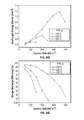
- FIG. 28 a is a graph of electric field-electric displacement loops for a dielectric composite according to some embodiments.
- FIG. 28 b is a graph of electric field-electric displacement loops for a dielectric composite according to some embodiments.
- FIG. 28 c is a graph of electric field-electric displacement loops for a dielectric composite according to some embodiments.
- FIG. 28 d is a graph of discharged energy density and charge-discharge efficiency, respectively, versus electric field, for the dielectric composite of FIGS. 28 a - 28 c;
- FIG. 28 e is a graph of discharged energy density and charge-discharge efficiency, respectively, versus electric field, for the dielectric composite of FIGS. 28 a - 28 c;
- FIG. 29 a is a graph of the discharged energy density and charge-discharge efficiency versus electric field for one conventional polymer dielectric material and a dielectric composite film according to some embodiments, at various temperatures;
- FIG. 29 b is a graph of the discharged energy density and charge-discharge efficiency versus electric field for one conventional polymer dielectric material and a dielectric composite film according to some embodiments, at various temperatures;
- FIG. 30 is a graph of the discharged energy density and charge-discharge efficiency versus electric field for thermally and photo-cross-linked dielectric composite films according to some embodiments.
- FIG. 31 is a photograph of a winding test of dielectric composite films according to some embodiments.
- FIG. 32 a is a photograph of an experimental setup for a bending test of dielectric composite films according to some embodiments
- FIG. 32 b depicts photographs of bending tests of dielectric composite films according to some embodiments.
- FIG. 33 is a graph of the dependence of the Young's modulus on temperature of conventional high-Tg polymer dielectrics and polymer dielectrics according to some embodiments;
- FIG. 34 a depicts the dielectric response of dielectric composite films according to some embodiments after winding and bending tests
- FIG. 34 b depicts the dielectric response of dielectric composite films according to some embodiments after winding and bending tests
- FIG. 35 a is a graph of the discharged energy density and charge-discharge efficiency, respectively, versus electric field, measured at 15° C., for dielectric composite films according to some embodiments after winding and bending tests;
- FIG. 35 b is a graph of the discharged energy density and charge-discharge efficiency, respectively, versus electric field, measured at 150° C., for dielectric composite films according to some embodiments after winding and bending tests;
- FIG. 35 c is a graph of the discharged energy density and charge-discharge efficiency, respectively, versus electric field, measured at 250° C., for dielectric composite films according to some embodiments after winding and bending tests;
- FIG. 35 d is a graph of the discharged energy density and charge-discharge efficiency, respectively, versus electric field, measured at 250° C., for dielectric composite films according to some embodiments after winding and bending tests;
- FIG. 36 a shows SEM images of dielectric composite films according to some embodiments after winding and bending tests.
- FIG. 36 b shows SEM images of dielectric composite films according to some embodiments after winding and bending tests.
- dielectric composites that can function at elevated temperatures and that comprise polymers and dielectric fillers.
- the polymers advantageously not degrade or undergo flow at temperatures below 250° C.
- the fillers are preferably ceramic fillers.
- the dielectric composites are characterized by an operating temperature of greater than 250° C. to a temperature of 350° C. and an operating electrical field strength of at least 250 megavolt (mV)/meter.
- the dielectric composites are manufactured by blending the polymer with the dielectric filler to form the dielectric composites.
- the dielectric composites are then shaped to form objects that may be used in articles such as capacitors.
- an article comprises a capacitor that comprises a first electrode and a second electrode that is opposedly disposed to the first electrode. Disposed between the two opposing electrode surfaces is the disclosed dielectric composite.
- the polymer is an organic polymer and has a softening point or flow point that is greater than 250° C., preferably greater than 300° C. and more preferably greater than 325° C.
- the softening point or flow point is preferably the glass transition temperature (Tg) of the polymer measured in a differential scanning calorimeter at rate of temperature change of 5° C./minute in a nitrogen atmosphere.
- the organic polymers may comprise a crosslinked polymer, a thermoplastic polymer or a combination comprising a crosslinked polymer and a thermoplastic polymer.
- the organic polymer may comprise a block copolymer, a diblock copolymer, a star block copolymer, a triblock copolymer, a dendrimer, an ionic copolymer, a polyelectrolyte, or the like.
- thermoplastic polymers are polybenzoxazoles, polyphthalamides, polyimides, polyamide-imides, polysulfonamides, polyarylates, polyaramids, polyetherketones, polyether ether ketones, or the like, or a combination thereof. Copolymers of these thermoplastic polymers with polysiloxanes may be used if desirable.
- crosslinked polymers are epoxy polymers, unsaturated polyester polymers, polyimide polymers, bismaleimide polymers, bismaleimide triazine polymers, cyanate ester polymers, benzoxazine polymers, benzocyclobutene polymers, acrylics, polyalkyds, phenol-formaldehyde polymers, novolacs, resoles, melamine-formaldehyde polymers, urea-formaldehyde polymers, hydroxymethylfurans, unsaturated polyesterimides, or the like, or a combination thereof.
- Exemplary organic polymers are crosslinked polymers.
- An exemplary organic polymer for use in the dielectric composite is crosslinked benzocyclobutene.
- An even more preferred organic polymer is crosslinked divinyltetramethyldisiloxane-bis(benzocyclobutene). The structure of divinyltetramethyldisiloxane-bis(benzocyclobutene) prior to crosslinking is shown in the formula (1)
- the organic polymer is used in amounts of 70 to 95 weight percent (wt %), preferably 80 to 93 wt % and more preferably 85 to 92 wt %, based on a total weight of the dielectric composite.
- the dielectric fillers may include ceramics. It is desirable for the dielectric fillers to be nanometer or micrometer sized fillers. Nanometer sized fillers are those having a largest dimension that ranges from 5 to 100 nanometers, preferably 10 to 90 nanometers and preferably 20 to 75 nanometers. Nanometer sized fillers are termed nanofillers. A term prefaced with “nano” have a largest dimension of 5 to 100 nanometers. Micrometer sized fillers are those having a largest dimension that ranges from 101 nanometers to 5000 nanometers (5 micrometers), preferably 150 to 3000 nanometers and more preferably 200 to 2000 nanometers. Micrometer sized fillers are termed microfillers and are prefaced with the term “micro”.
- the dielectric fillers may have any shape and can be a 1-dimensional filler (e.g., a nanowire), a 2-dimensional geometry (e.g., a platelet) or a three dimensional geometry (e.g., a spherical particle such as a buckyball).
- a 1-dimensional filler e.g., a nanowire
- 2-dimensional geometry e.g., a platelet
- a three dimensional geometry e.g., a spherical particle such as a buckyball
- Examples of dielectric filler shapes include wires, tubes, platelets, spheres, ellipsoids, pyramids, cones, or the like, or a combination thereof.
- the dielectric fillers may be nanowires, nanotubes, nanodots, nanoplatelets, nanorods, nanoparticles that have spherical shapes, nanosheets, microwires, microtubes, microdots, microplatelets, microrods, microparticles that have spherical shapes, microsheets, or the like, or a combination thereof.
- the 1-dimensional fillers and 2-dimensional fillers can have aspect ratios of 5 to 100,000, preferably 10 to 50,000 and more preferably 100 to 5,000.
- the dielectric fillers may be a metal oxide, a metal carbide, a metal oxycarbide, a metal nitride, a metal oxynitride, a metal boride, a metal borocarbide, a boronitride, a metal silicide, a metal iodide, a metal bromide, a metal sulfide, a metal selenide, a metal telluride, a metal fluoride, a metal borosilicide, or the like, or a combination thereof.
- dielectric fillers examples include alumina, magnesia, zirconia, titania, antimony tin oxide, barium titanate, calcium copper titanate, lead titanate, lead magnesium titanate, barium neodymium titanate, lead zirconium titanate, strontium titanate, calcium titanate, boron nitride, hexagonal boron nitride, aluminum nitride, silicon nitride, silicon carbide, diamond of natural or synthetic origin, or the like, or a combination thereof.
- the filler particles can be of the various physical forms of each type listed above and the particles may be hybrids of the materials mentioned and have stoichiometric and non-stoichiometric mixed oxides, nitrides and carbides. More specific examples of these include Al 2 O 3 , AIN, MgO, ZnO, BeO, BN, Si 3 N 4 , SiC, SiO, and SiO 2 with mixed stoichiometric and non-stoichiometric combinations.
- a preferred dielectric filler are boron nitride nanosheets.
- dielectric fillers can also contain reactive surfaces to form intimate covalently bonded hybrid organic-inorganic homogeneous materials.
- the inorganic filler particles have been surface treated to introduce surface functional groups that allow for the essentially complete co-reactivity with the organic polymer.
- the functional groups may comprise at least one of hydroxyl, carboxylic, amine, epoxide, silane and vinyl groups.
- the dielectric fillers may be present in the dielectric composite in an amount of 5 to 30 wt %, preferably 7 to 20 wt % and more preferably 8 to 15 wt %, based on the total weight of the dielectric composite.
- the organic polymer along with the dielectric filler may be blended in the appropriate blending equipment to produce the dielectric composite.
- the organic polymer along with the dielectric filler may be dry blended, melt blended and/or solution blended in the equipment to produce the composite in the form of a powder, pellets, briquettes, or the like.
- the dielectric composite can be dry blended to form a mixture in a device such as a Henschel mixer or a Waring blender prior to being fed to an extruder, where the mixture is melt blended.
- a portion of the organic polymer can be premixed with the dielectric filler to form a dry preblend. The dry preblend is then melt blended with the remainder of the organic polymer in an extruder.
- some of dielectric composite can be fed initially at the mouth of the extruder while the remaining portion of the dielectric composite is fed through a port downstream of the mouth.
- Blending of the dielectric composite involves the use of shear force, extensional force, compressive force, ultrasonic energy, electromagnetic energy, thermal energy or combinations comprising at least one of the foregoing forces or forms of energy and is conducted in processing equipment wherein the aforementioned forces are exerted by a single screw, multiple screws, intermeshing co-rotating or counter rotating screws, non-intermeshing co-rotating or counter rotating screws, reciprocating screws, screws with pins, barrels with pins, rolls, rams, helical rotors, or combinations comprising at least one of the foregoing.
- Blending involving the aforementioned forces or forms of energy may be conducted in machines such as single or multiple screw extruders, Buss kneader, Henschel, helicones, Ross mixer, Banbury, roll mills, molding machines such as injection molding machines, vacuum forming machines, blow molding machine, or then like, or combinations comprising at least one of the foregoing machines.
- machines such as single or multiple screw extruders, Buss kneader, Henschel, helicones, Ross mixer, Banbury, roll mills, molding machines such as injection molding machines, vacuum forming machines, blow molding machine, or then like, or combinations comprising at least one of the foregoing machines.
- the dielectric composite may then be molded to take its desired shape and subjected to crosslinking.
- Crosslinking may be brought about by subjecting the dielectric composite to thermal energy, electromagnetic radiation or to a combination of electromagnetic radiation and thermal energy.
- Electromagnetic radiation can include UV radiation, electron beam energy, x-ray radiation, infrared radiation, microwave radiation, or a combination thereof.
- the crosslinked dielectric composite may be used in articles such as, for example, a capacitor.
- the boron nitride nanosheets are exfoliated using the organic polymer that is solvated in a solvent.
- the dielectric composite is prepared by first manufacturing the boron nitride nanosheets from boron nitride powders using a known solution phase exfoliation method, as described in Coleman, J. N. et al. Two-dimensional nanosheets produced by liquid exfoliation of layered materials. Science 331, 568-571 (2011).
- the boron nitride nanosheets are dispersed in a solvent to form a first solution at an appropriate concentration.
- a second solution comprising the divinyltetramethyldisiloxane-bis(benzocyclobutene) of the formula (1) above.
- the first solution and the second solution is mixed for a period of time effective to facilitate exfoliation of the boron nitride nanosheets.
- the solution mixture may be subjected to sonication to facilitate exfoliation.
- mixing of the first and the second solution may be conducted in an extruder.
- the dielectric composite may be melt blended by blending the divinyltetramethyldisiloxane-bis(benzocyclobutene) with the boron nitride nanosheets to produce exfoliation of the boron nitride nanosheets.
- the exfoliated dielectric composite may then be disposed onto a substrate and subjected to curing using thermal energy or electromagnetic radiation.
- FIG. 1 depicts a schematic representation of a polymer composite according to one aspect of the present disclosure.
- the dielectric composite 100 includes polymer matrix comprising cross-linked divinyltetramethyldisiloxane-bis(benzocyclobutene) (c-BCB) 102 and a plurality of boron nitride nanosheets (BNNS) 104 dispersed in the polymer matrix.
- c-BCB cross-linked divinyltetramethyldisiloxane-bis(benzocyclobutene)
- BNNS boron nitride nanosheets
- the concentration of BNNS in a c-BCB and BNNS composite is approximately 10% by volume.
- the concentration of the BNNS may be less than 20% by volume, less than 15% by volume, less than 10% by volume, or any other suitable concentration.
- the c-BCB polymer matrix may be cross linked in any suitable manner.
- the first solution and the second solution described above may be thermally cross-linked, such as with a solvent baking and a curing process.
- a c-BCB polymer matrix may be photo-cross-linked by exposure to UV radiation.
- photo-crosslinking may allow for a c-BCB/BNNS polymer composite to be photo-patternable such that a desired pattern may be formed by using an optical mask during crosslinking.
- the dielectric composites described herein exhibit a stable dielectric response at high temperatures and under high applied electric fields.
- a polymer composite including BNNS which help to reduce electrical conduction, may allow the polymer composite to have a higher working temperature than conventional polymers, especially when under high applied electric fields.
- the dielectric composite may be used in applications and/or environments in which the operating temperature and/or electric field strength exceed the limits of other commercially available polymeric dielectric materials.
- the dielectric composite disclosed herein may have a an operating temperature of at least 350° C. and may be used with applied electric fields of at least 250 MVm ⁇ 1 ; in other embodiments, the maximum operating electric field strength may be at least 350 MVm ⁇ 1 .
- the dielectric composites disclosed herein may have a stable dielectric constant over a wide range of operating temperatures and varying applied electric fields.
- the dielectric composite has a dielectric constant that varies by less than 2% over a temperature range of 25° C. to 300° C., with an applied alternating electric field having a frequency of 10 4 Hz.
- the dielectric constant of other commercially available dielectric composites varies by 8% or more over the same temperature range.
- the dielectric composite has a dielectric constant that varies by less than 2% over a temperature range of 25° C. to 300° C., with an applied direct current (DC) bias with an electric field strength of 50 MVm ⁇ 1 .
- DC direct current
- FIG. 2 is a schematic representation of one embodiment of a capacitor according to some aspects of the present disclosure.
- the capacitor 200 includes a first electrode 210 , a second electrode 220 , and a polymer dielectric 230 disposed between the electrodes.
- the dielectric composite described herein may be incorporated into the capacitor.
- a capacitor may include a first metal electrode, a second metal electrode, and a dielectric composite such as a c-BCB/BNNS dielectric composite disposed between the electrodes.
- Leads 240 are attached to the electrodes to electrically couple the capacitor to a suitable electronic system.
- a capacitor may have any suitable configuration, including, but not limited to a flat or parallel plate geometry including one or more layers, or a rolled or wound configuration.
- the dielectric composite and the method of manufacturing the composite is now detailed in the following non-limiting example.
- This example was conducted to determine the dielectric properties of the dielectric composites disclosed herein. It also demonstrates the method of manufacturing the dielectric composites disclosed herein. The dielectric composites disclosed herein are also compared with high temperature polymer dielectrics.
- Dipropylene glycol dimethyl ether (DMM), benzocyclobutene (BCB) monomers and b-staged BCBs (partially polymerized) with the number average molecular weight of ⁇ 25 k were provided by Dow Chemical.
- Boron nitride powders were purchased from Sigma-Aldrich.
- the high-T g polymer dielectric films were provided by PolyK Technologies.
- the polyimide)(Kapton®) films were vacuum dried overnight at 70° C. before use. All the other materials were used as received.
- boron nitride nanosheets were prepared from boron nitride powders using a solution phase exfoliation method.
- BNNSs were first dispersed in DMM at a concentration of 5 mg mL ⁇ 1 to form the first solution 100 mg BCB monomers were dissolved in 2 mL DMM and stirred for 2 hours to form the second solution. Afterwards the first solution was mixed with the second solution (i.e., the DMM solution of BNNSs was mixed with BCB solution in proportion), and the mixture was first stirred for 10 minutes and then sonicated for 5 minutes using a tip-type sonicator (175 W).
- the mixture was drop-cast on a glass slide and subject to a soft solvent baking at 120° C. for 30 minutes, which was followed by a hard curing at 250° C. for 2 hours under a nitrogen (N 2 ) atmosphere.
- the film was peeled off after soaking in water for 5 minutes.
- the film thickness can be varied by tuning the concentration of the cast solution.
- the thickness of films used for electrical characterizations is within the range of 6-12 ⁇ m.
- DMM solution of b-staged BCB mixed with BNNSs was used to cast a film on Si wafer by spin-coating.
- the spin-coated film was subject to a 20-min UV-exposure in an UV cross-linker (XL-1500, Spectroline) equipped with UV tubes (BLE-1T155, Spectroline).
- the thickness of the film can be varied by changing the solution concentration and parameters of spin-coating. Typically, a 30 wt % solution spin-coated at 700 rpm yields a 4- ⁇ m-thick film, which, after curing at 250° C. for 15 min under N 2 , achieves the same level of performance to the thermally cross-linked films.
- the material was spin-coated on Si wafer from a 20 wt % solution of b-staged BCB mixed with BNNSs at 3,000 rpm, and then covered with an optical mask before UV irradiation. Afterwards, the material was developed by using DMM and dried.
- FTIR Fourier-transform infrared
- ATR attenuated total reflectance
- DSC Differential scanning calorimetry
- XRD X-ray diffraction
- TGA Thermogravimetric analysis
- TEM Transmission electron microscopy
- SEM Scanning electron microscopy
- Gold electrodes of a diameter of 6 mm and a thickness of 60 nm were sputtered on both sides of the polymer films for the electrical measurements.
- Dielectric spectra were acquired over a broad temperature range using a Hewlett Packard 4284A LCR meter in conjunction with a Delta Design oven model 2300.
- Dielectric spectra under DC bias were collected with the same equipment along with a Hewlett Packard 4140B pA meter/voltage source, a KEPCO BOP 1000M amplifier and a protective circuit. Conduction currents were obtained under an electric field provided by a Hewlett Packard 4140B pA meter/voltage source and TREK model 2210 amplifier. High-field electric displacement-electric field loops were collected using a modified Sawyer-Tower circuit, where the samples were subject to a triangular unipolar wave with a frequency of 10 Hz. Dielectric breakdown strength measurements were performed on a TREK P0621P instrument using the electrostatic pull-down method under a DC voltage ramp of 500 V s ⁇ 1 . Young's moduli were derived from strain-stress curves measured with a TA RSA-G2 Solids Analyzer, using a constant linear stretching rate of 0.02% s ⁇ 1 .
- T ext is the surrounding temperature
- h convective heat transfer coefficient
- ⁇ sb is Stefan-Boltzmann constant
- ⁇ emissivity of the surfaces. Due to symmetry only 1 ⁇ 8 of the volume is modeled.
- the system mesh size is set as 120 ⁇ 120 ⁇ 30 with a grid spacing of 0.33 mm.
- FIG. 3 a is a schematic representation of one embodiment of the preparation of a c-BCB/BNNS polymer dielectric film.
- FIGS. 3 b -3 c are transmission electron microscope (TEM) images of BNNSs exfoliated from h-BN powders. The inset shows the electron diffraction pattern of BNNSs showing the hexagonal symmetry.
- FIG. 3 d depicts the chemical structures of BCB monomers, and
- FIG. 3 e depicts the repeating unit of cross-linked BCB.
- FIGS. 3 f -3 g are photographs of a 10 flm thick c-BCB/BNNS film wrapped on a glass tube with a 4 mm diameter, and a deformed 10 f.Lm thick c-BCB/BNNS film, respectively.
- FIGS. 3 h -3 j show a photo-patterned c-BCB/BNNS film on a Si wafer; dark regions correspond to the c-BCB/BNNS.
- FIG. 4 shows an ATR-FTIR spectrum of c-BCB and c-BCB/BNNS according to some embodiments.
- the presence of BNNSs is confirmed by the emerging characteristic peak centered at 1370 cm ⁇ 1 in the spectrum of c-BCB/BNNS (the dielectric composite), which is attributed to the in-plane ring vibration of h-BN.
- the absorption bands located at around 1,500, 1,000-1,080 and 640-880 cm ⁇ 1 are attributed to the vibrations of tetrahydronaphthalene, Si—O—Si and C—H structures, respectively, in c-BCB.
- FIG. 5 is a graph of the gel content of c-BCB in c-BCB/BNNS as a function of BNNS content according to some embodiments.
- the analysis was performed by solvent swelling and extraction of samples in DMM heated to reflux for 12 hours. The gels were then dried at 90° C. in vacuum to give the dry weight of the insoluble component. The gel contents were a fraction of dry insoluble weight to the initial weight.
- the gel content of c-BCB is independent of the BNNS content, indicating that the presence of BNNSs does not affect the cross-linking of BCB.
- FIGS. 6 a and 6 b show differential scanning calorimetry (DSC) curves and x-ray diffraction (XRD) patterns, respectively, of c-BCB and c-BCB/BNNS 10 vol % of BNNSs, according to one embodiment.
- the inset shows a 2-D X-ray pattern of the c-BCB/BNNS with 10 vol % (volume percent) of BNNSs.
- XRD patterns confirm amorphous structures for c-BCB in both cases, and the uniform diffraction ring shown in the 2-D X-ray diffraction indicates a random orientation of BNNSs in the polymer matrix.
- FIGS. 7 a and 7 b show TGA and DMA curves, respectively, of c-BCB/BNNS of one embodiment.
- the inset in FIG. 7 a shows TGA recorded from 250 to 450° C.
- the result of TGA conducted in N2 atmosphere indicates a decomposing temperature at around 450° C., and the TGA performed in air shows the onset of degradation at ⁇ 350° C.
- the result of DMA suggests that no glass transition occurs in the material below 350° C.
- FIGS. 8 a and 8 b are cross-sectional SEM images of one embodiment of c-BCB/BNNSs with 10 vol % of BNNSs.
- cross-linked pristine BCB (the c-BCB polymer) ( ⁇ 95 wt % gel content) exhibited a high Tg (>350° C.), low volume conductivity ( ⁇ 1 ⁇ 10 ⁇ 17 S m ⁇ 1 ), low dissipation factor ( ⁇ 0.15% at 10 3 Hz) and small variation ( ⁇ 3%) in dielectric constant at weak field from room temperature to 300° C.
- the conduction loss of c-BCB polymer was found to increase sharply, e.g., a volume conductivity of ⁇ 4 ⁇ 10 ⁇ 12 S m ⁇ 1 and conduction loss of ⁇ 18% was found under an electric field of 200 MVm ⁇ 1 at 150° C.
- c-BCB/BNNS dielectric composite exhibit significantly suppressed high-field electrical conduction at elevated temperatures.
- the electrical conductivity was found to decrease from 4 ⁇ 10 ⁇ 12 to 9.2 ⁇ 10 ⁇ 14 S m ⁇ 1
- the conduction loss was found to decrease from 18% to 3% going from the c-BCB polymer to the c-BCB/BNNS dielectric composite under an applied field of 200 MVm ⁇ 1 at 150° C.
- FIG. 9 a is a graph of the frequency dependence of dielectric constant and dissipation factor of c-BCB polymer and the c-BCB/BNNS dielectric composite with different filler contents according to some embodiments.
- FIG. 9 b is a graph of the dielectric constant and dissipation factor of the c-BCB/BNNS dielectric composite at 10 3 Hz as a function of BNNS content.
- FIG. 9 c is a graph of the temperature dependence of dielectric constant and dissipation factor of c-BCB polymer and the c-BCB/BNNS dielectric composite with 10 vol % of BNNSs.
- the dielectric constant of the c-BCB/BNNS dielectric composite with 10 vol % of BNNSs is found to increase by about 5 to 15%, preferably 8 to 12% compared to the pristine c-BCB polymer, which may be attributable to the higher dielectric constant of h-BN (i.e. 4-7) relative to that of c-BCB polymer.
- the dielectric constant of the dielectric composite containing 5 to 15 vol % of the dielectric filler is 2.8 to 3.5, preferably 2.9 to 3.25 at 1000 Hz when measured in a temperature range from 25 to 350° C., preferably 30 to 325° C., and more preferably 35 to 300° C.
- FIG. 10 shows electric displacement-electric field (D-E) loops of the c-BCB polymer ( FIGS. 10 a -10 b ) and the c-BCB/BNNS dielectric composite with 10 vol % of BNNSs ( FIGS. 10 c -10 d ) according to some embodiments, at room temperature and at 150° C.
- FIG. 10 e is a schematic D-E loop of a dielectric material with the discharged energy density (U d ) represented by the area colored in purple and energy loss (U l ) indicated by the area painted orange.
- the total stored energy density (U) equals U d plus U l
- the conduction loss can be calculated as 100% ⁇ U l /U.
- FIG. 10 f depicts the conduction loss of the c-BCB polymer and the c-BCB/BNNS dielectric composite at 150° C. as a
- FIG. 11 is a graph of the Young's moduli of c-BCB polymer and the c-BCB/BNNS dielectric composite with 10 vol % BNNS of one embodiment at various temperatures.
- Young's modulus elastic modulus
- the increased modulus provides dimensional stability at elevated temperatures when compared with unfilled polymers.
- the dielectric composites thus display a unique combination of thermal and dimensional stability and dielectric constant at temperatures of 25 to 350° C., preferably 30 to 300° C.
- FIG. 12 a is a graph of the current density of the c-BCB polymer and the c-BCB/BNNS dielectric composite with 10 vol % of BNNSs of one embodiment under a DC bias of 50 MVm ⁇ 1 at various temperatures.
- FIG. 12 b is a graph of the volume conductivity under an applied field of 50 MVm ⁇ 1 as a function of temperature. From the FIGS. 12 a and 12 b , it may be seen that current density and volume conductivity is of the dielectric composite is reduced compared with that of the unfilled polymer in a temperature range of 25 to 300° C., preferably 30 to 250° C.
- FIG. 13 a shows Weibull plots of the c-BCB/BNNS dielectric composite with various BNNS contents according to some embodiments.
- FIG. 13 b shows the Weibull breakdown strength of the embodiments of the c-BCB/BNNS dielectric composite as a function of the filler content.
- FIG. 13 c shows Weibull plots of one embodiment of the c-BCB/BNNS dielectric composite with 10 vol % of BNNSs at different temperatures.
- FIG. 13 d is a graph of the Weibull breakdown strength of the c-BCB polymer and the c-BCB/BNNS dielectric composite as a function of temperature. From the FIG. 13 d , it may be seen that the Weibull strength is increased by at least 100 MVm ⁇ 1
- FIG. 14 shows the conduction current density of the c-BCB polymer ( FIG. 14 a ) and the c-BCB/BNNS dielectric composite with 10 vol % BNNSs as a function of electric field strength at various temperatures. It has been discovered that the current density of the c-BCB/BNNS dielectric composite may be much lower than that of the c-BCB polymer at comparable temperatures and field strengths. FIG. 14 also displays a clear trend that conduction current density increased exponentially over electric field; without wishing to be bound by any particular theory, this may imply that solid state hopping conduction is a plausible conduction mechanism in these materials.
- Equation 1a are also presented in FIG. 14 ; the curve fits are found to agree well with the experimental data, suggesting that hopping is the major conduction mechanism in these materials.
- the electrical conductivity of polymer dielectrics that follow the hopping mechanism is no longer ohmic (non-linear relationship between current and field) but exponentially increases with the field strength when the energy gained between traps becomes comparable to the thermal energy which causes de-trapping at lower field strengths. With a further increase of the applied electric field, when the energy gained between traps becomes comparable to the trap depth, the electrical conductivity would increase drastically.
- the thermal activation energy of conductivity reflects the depth of traps, and thus determines the likelihood of carriers running out of traps at a given condition to participate the conduction process. It is thus informative to investigate the activation energy of the materials.
- FIG. 15 is a graph of the dependence of A on temperature for the c-BCB polymer and the c-BCB/BNNS dielectric composite with 10 vol % of BNNSs according to one embodiment. The values of A used for the linear fits are extracted from the curve fits in FIG.
- FIGS. 16 a -16 b are Arrhenius plots of the conductivity of c-BCB and c-BCB/BNNS with 10 vol % of BNNSs, respectively, under various electric fields.
- the average activation energies determined from Equation 4a are 0.77 eV and 0.94 eV, for the c-BCB and c-BCB/BNNS, respectively.
- the dielectric properties of one embodiment of a c-BCB/BNNS polymer composite have been evaluated along with the state-of-the-art high-temperature capacitor-grade polymer films (also called conventional polymer dielectrics) including polycarbonate (PC), poly(ether ether ketone) (PEEK), polyetherimide (PEI), fluorine polyester (FPE) and polyimide (Kapton PI).
- PC polycarbonate
- PEEK poly(ether ether ketone)
- PEI polyetherimide
- FPE fluorine polyester
- Kapton PI polyimide
- the dielectric constant K and dissipation factor DF were analyzed as a function of temperature and frequency. It has been discovered that at 10 4 Hz, which is the frequency of interest for common power conditioning applications, a minor variation in K with temperature, i.e. ⁇ 1.7%, is seen in c-BCB/BNNS from room temperature to 300° C., while FPE, the next best dielectric investigated in this study, shows a K variation of over 8% at 300° C. relative to room temperature. Moreover, it has been found that the temperature coefficient of K for the c-BCB/BNNS dielectric composite is around 65 ppm ° C. ⁇ 1 , compared to 308 and 498 ppm ° C.
- DF of the c-BCB/BNNS dielectric composite at 10 4 Hz only increases from 0.09% to 0.13% with increasing temperature up to 300° C. While Kapton shows similar stability of DF with temperature under DC bias to the c-BCB/BNNS dielectric composite, appreciable increases in DF have been observed in all the other polymer dielectrics, e.g. DF of FPE jumps from 0.22% at room temperature to 1.35% at 280° C. In view of the above, c-BCB/BNNS may offer a substantially more stable K and DF in the frequency range of 10 2 to 10 6 Hz at elevated temperatures compared to known other high T g polymer dielectrics known in the art.
- FIGS. 17 a and 17 b are graphs of the temperature dependence of dielectric constants and dissipation factors, respectively, of one embodiment of the c-BCB/BNNS dielectric composite with 10 vol % of BNNSs and the high-T g polymer dielectrics.
- FIG. 17 c depicts the percentage change of dielectric constants of the c-BCB/BNNS dielectric composite and the high-T g polymer dielectrics relative to the room-temperature values as a function of temperature
- 17 d shows the temperature coefficients of the dielectric constant of the c-BCB/BNNS dielectric composite and the high-T g polymer dielectrics (shown in Table 1 excluding the c-BCB—these are also referred to as conventional polymer dielectrics) over various temperature ranges.
- FIG. 17 e is a graph of the temperature dependence of dissipation factors of the c-BCB/BNNS dielectric composite and high-T g polymer dielectrics under a DC bias of 50 MVm ⁇ 1
- FIG. 17 f depicts the frequency dependence of dielectric constants and dissipation factors of the c-BCB/BNNS dielectric composite at different temperatures.
- FIG. 18 shows the frequency dependence of the dielectric constant and dissipation factor of one embodiment of the c-BCB/BNNS dielectric composite with 10 vol % of BNNSs and the high-T g polymer dielectrics at room temperature. Although many of the high-temperature polymer dielectrics show good frequency-stability of dielectric constant, their dissipation factors begin to increase at around 104 Hz. In contrast, the c-BCB/BNNS dielectric composite exhibits excellent stability of both dielectric constant and dissipation factor over the entire frequency range.
- FIGS. 19 a -19 b are graphs of the temperature dependence of the dielectric constant and percentage change of dielectric constant, respectively, of one embodiment of the c-BCB/BNNS dielectric composite with 10 vol % of BNNSs and the high-T g polymer dielectrics at 10 4 Hz under a DC bias of 50 MVm ⁇ 1 .
- the percentage change of dielectric constant of the c-BCB/BNNS dielectric composite is only 1.6% at 250° C., and increases to ⁇ 4% at 300° C.
- all the conventional high temperature polymer dielectrics tested herein display a variation of dielectric constant larger than 10% within the same temperature range.
- FIGS. 20 a -20 c are graphs of the frequency dependence of the dialectic constant and dissipation factor of Kapton, FPE, and PEI, respectively, at different temperatures. These results indicate that the dissipation factors of these high-temperature polymer dielectrics may be unstable over various frequency ranges at certain temperatures, and the variations of dielectric constant from room temperature to 250° C. may be relatively large.
- FIGS. 21 a -21 c are graphs of the percentage change of dielectric constant of one embodiment of the c-BCB/BNNS dielectric composite with 10 vol % of BNNSs and high-temperature polymer dielectrics at 150° C., 200° C. and 250° C., respectively, relative to room temperature as a function of frequency.
- the c-BCB/BNNS dielectric composite may outperform many other high-Tg polymer dielectrics at temperatures ranging from 150 to 250° C. in terms of the discharged energy density (U e ) and the charge-discharge efficiency ( ⁇ ).
- U e discharged energy density
- ⁇ charge-discharge efficiency
- the c-BCB/BNNS dielectric composite can discharge an U e exceeding 2.2 J cm ⁇ 3 under an applied electric field of 400 MV m ⁇ 1 with a ⁇ of larger than 90% at 150° C.
- the c-BCB/BNNS dielectric composite may have a U e of 2 Jcm ⁇ 3 under an applied field of 400 MVm ⁇ 1 , which is twice that of PEI, as well as a more than 1.5 times higher ⁇ than PEI.
- the c-BCB/BNNS dielectric composite may be functional up to an applied field of 400 MVm ⁇ 1 with an U e of ⁇ 1.8 J cm ⁇ 3 .
- the ⁇ of the c-BCB/BNNS dielectric composite at 150° C. i.e. ⁇ 97%, is the same as that of BOPP at 70° C.
- FIG. 22 depicts graphs of the discharged energy density and charge-discharge efficiency of one embodiment of the c-BCB/BNNS dielectric composite with 10 vol % of BNNSs and high-T g polymer dielectrics measured at 150° C. ( FIGS. 22 a -22 b ), 200° C. ( FIGS. 22 c -22 d ), and 250° C. ( FIGS. 22 e -22 f ).
- FIG. 23 a -23 c are graphs of D-E loops, discharged energy density, and charge-discharge efficiency, respectively, of PC at 150° C.
- FIG. 24 a -24 c are graphs of D-E loops, discharged energy density, and charge-discharge efficiency, respectively, of PEEK at 150° C.
- FIGS. 25 a -25 b are graphs of D-E loops, FIG. 25 c is a graph of discharged energy density, and FIG. 25 d is a graph of the charge-discharge efficiency of PEI at elevated temperatures.
- FIGS. 26 a -26 c are graphs of D-E loops, FIG. 26 d is a graph of discharged energy density, and FIG.
- FIGS. 26 e is a graph of the charge-discharge efficiency of FPE at elevated temperatures.
- FIGS. 27 a -27 c are graphs of D-E loops, FIG. 27 d is a graph of discharged energy density, and FIG. 27 e is a graph of the charge-discharge efficiency of Kapton at elevated temperatures.
- FIGS. 28 a -28 c are graphs of D-E loops, FIG. 28 d is a graph of discharged energy density, and FIG. 28 e is a graph of the charge-discharge efficiency of one embodiment of the c-BCB/BNNS dielectric composite with 10 vol % BNNSs at elevated temperatures.
- FIGS. 29 a -29 b show the discharged energy density and charge-discharge efficiency of BOPP and one embodiment of the c-BCB/BNNS dielectric composite with 10 vol % of BNNSs derived from D-E loops at room temperature and elevated temperature, respectively.
- the c-BCB/BNNS dielectric composite shows higher discharged energy density and very similar charge-discharge efficiency relative to BOPP at comparable fields. It has been discovered that at 150° C. and under a field of 200 MVm ⁇ 1 , the c-BCB/BNNS dielectric composite still displays higher discharged energy density and very similar charge-discharge efficiency relative to those of BOPP measured at 70° C. and 200 MVm ⁇ 1 . Since film capacitors in the power inverter of electric vehicles are usually operated under 200 MVm ⁇ 1 , this data indicates that by replacing BOPP with BCB/BNNS, the secondary cooling system for capacitors in electric vehicles may be not be necessary, as discussed above.
- a c-BCB/BNNS dielectric composite polymer composite may be photo-cross-linked, and therefore may be photo-patternable. It has been discovered that the dielectric properties of photo-cross-linked the c-BCB/BNNS dielectric composite films do not differ substantially from thermally cross-linked films.
- FIG. 30 shows the discharged energy density and charge-discharge efficiency of thermally cross-linked BCB/BNNS and photo/thermally cross-linked BCB/BNNS with 10 vol % of BNNSs at 250° C.
- FIG. 31 is a photograph of a winding test in which one embodiment of a the c-BCB/BNNS dielectric composite film with 10 vol % of BNNSs is wrapped on a glass tube for three turns.
- the second is a bending test, in which the BCB/BNNS film strip is repeatedly bent and unbent for 20,000 rounds; each round is programmed to be accomplished in 5 seconds.
- FIGS. 32 a -32 b are photographs of the experimental setup for the bending test and one bending and unbending cycle, respectively.
- FIG. 33 is a plot of the Young's moduli of the the c-BCB/BNNS dielectric composite film with 10 vol % of BNNSs and the other high-T g polymer dielectrics at different temperatures.
- the dielectric stability of the wound and bended materials was investigated by studying the frequency dependent dielectric properties at both room temperature and elevated temperature.
- High-temperature high-electric-field performances of all the samples were studied by conducting a charge-discharge experiment at 150° C. and 250° C. as a function of electric fields.
- FIG. 35 depicts graphs of the discharged energy density and charge-discharge efficiency for one embodiment of a the c-BCB/BNNS dielectric composite film with 10 vol % of BNNSs before and after winding and bending tests, measured at 150° C. ( FIGS. 35 a and 35 b ) and at 250° C. ( FIGS. 35 c and 35 d ).
- FIG. 36 depicts cross-sectional SEM images of the the c-BCB/BNNS dielectric composite film with 10 vol % of BNNSs after winding ( FIG. 36 a ) and after bending ( FIG. 36 b ); no detectable cracks or flaws after winding and bending were found.
- embodiments of the c-BCB/BNNS dielectric composite materials are flexible, and that winding and bending does not affect the energy storage capabilities or dielectric response.
- transition term comprising encompasses the transition terms “consisting of” and “consisting essentially of”.
Abstract
Description


P(E)=1−exp(−(E/α)β)
where P(E) is the cumulative probability of electric failure, E is the measured breakdown field, the scale parameter α is the field strength for which there is a 63% probability for the sample to breakdown (Weibull breakdown strength), and the shape parameter β evaluates the scatter of data and a higher value of β represents greater dielectric reliability. Temperature coefficient of dielectric constant. The temperature coefficient of dielectric constant, τεr, for a given temperature range (from Ti to Tf), is defined as,
τεr=(K f −K i)/(K ref(T f −T i))
where Kref is the dielectric constant at room temperature, Ti and Tf are the low end and high end temperatures, respectively, and Ki and Kf are the dielectric constants at Ti and Tf, respectively.
where ρm and C are the density and heat capacity respectively. K is the thermal conductivity and E stands for the applied electrical field. In particular, evidenced by the experimental measurements, the electrical conductivity σ depends on the temperature T, having the characteristic form of
where the coefficients σ0 and A for each material at one specific applied electric field are calculated by fitting the measured data. Setting ∂T(x)/∂t=0 yields the steady-state temperature solution of Eq. (1), as
K∇ 2 T(x)+σ(x,T)E(x)2=0 (3)
The governing equation is then solved by finite element (FE) simulations using the commercial software COMSOl4.4. When the capacitor works, the thin slices of structures are packed by an enclosure, with the surrounding cooling liquid. Therefore, the capacitor is treated as an integrated body with a uniform applied electric field for each calculation. The geometries arising from the experimental setup are used in the FE model. As a result of laminar structure of capacitor in which the polymer has the relatively low thermal conductivity compared to the metallization, anisotropy in thermal conductivity is considered in the model. During the FE simulation, the heat flux at all the enclosure surfaces of the capacitor is contributed by both convective and radiative heat transfer arising from the surrounding cooling, with the form of
n·(−K∇T)=h(T−T ext)+σsbε(T 4 −T ext 4) (4)
Where Text is the surrounding temperature, h is convective heat transfer coefficient, σsb is Stefan-Boltzmann constant, and ε is emissivity of the surfaces. Due to symmetry only ⅛ of the volume is modeled. On the mesh sensitive study, the system mesh size is set as 120×120×30 with a grid spacing of 0.33 mm.
J(E,T)=2neλv*exp [−(eW/k B T)]*sin h(λeE/2k B T) (1a)
where n is the carrier concentration, λ the hopping distance, v the attempt-to-escape frequency, W the activation energy in eV, e the electric charge of the carriers, kB the Boltzmann constant. The curve fits of Equation 1a are also presented in
J(E)=A*sin h(BE) (2a)
where A and B are two lumped parameters. A can be considered as a function of temperature T as,
A(T)=2neλv*exp [−(eW/k B T)] (3a)
from which the activation energy can be obtained through a linear fit of the Arrhenius plot.
σ(T)=σ0*exp [−(Aq/k B T)] (4a)
where σ0 is the prefactor, A is the activation energy in eV, q is the electronic charge, and kB is the Boltzmann constant.
| TABLE 1 | ||||
| Tg | Thickness | Mass Density | ||
| Polymer | (° C.) | (μm) | Film Type | (g cm−3) |
| |
150 | 6 | Solution cast film | 1.21 |
| |
150 | 12 | Amorphous | 1.32 |
| PEEK | ||||
| PEI | 217 | 12 | Extruded film | 1.27 |
| FPE | 330 | 6 | Solution cast film | 1.21 |
| PI | 360 | 12 | Kapton -HN | 1.42 |
| c-BCB/BNNS | >350 | 6-12 | Solution cast film | 1.10 |
Claims (17)


Priority Applications (2)
| Application Number | Priority Date | Filing Date | Title |
|---|---|---|---|
| US15/165,087 US10020115B2 (en) | 2015-05-26 | 2016-05-26 | High temperature dielectric materials, method of manufacture thereof and articles comprising the same |
| US15/955,034 US11417466B2 (en) | 2015-05-26 | 2018-04-17 | High temperature dielectric materials, method of manufacture thereof and articles comprising the same |
Applications Claiming Priority (2)
| Application Number | Priority Date | Filing Date | Title |
|---|---|---|---|
| US201562166355P | 2015-05-26 | 2015-05-26 | |
| US15/165,087 US10020115B2 (en) | 2015-05-26 | 2016-05-26 | High temperature dielectric materials, method of manufacture thereof and articles comprising the same |
Related Child Applications (1)
| Application Number | Title | Priority Date | Filing Date |
|---|---|---|---|
| US15/955,034 Continuation US11417466B2 (en) | 2015-05-26 | 2018-04-17 | High temperature dielectric materials, method of manufacture thereof and articles comprising the same |
Publications (2)
| Publication Number | Publication Date |
|---|---|
| US20170162325A1 US20170162325A1 (en) | 2017-06-08 |
| US10020115B2 true US10020115B2 (en) | 2018-07-10 |
Family
ID=57394283
Family Applications (2)
| Application Number | Title | Priority Date | Filing Date |
|---|---|---|---|
| US15/165,087 Active 2036-10-18 US10020115B2 (en) | 2015-05-26 | 2016-05-26 | High temperature dielectric materials, method of manufacture thereof and articles comprising the same |
| US15/955,034 Active US11417466B2 (en) | 2015-05-26 | 2018-04-17 | High temperature dielectric materials, method of manufacture thereof and articles comprising the same |
Family Applications After (1)
| Application Number | Title | Priority Date | Filing Date |
|---|---|---|---|
| US15/955,034 Active US11417466B2 (en) | 2015-05-26 | 2018-04-17 | High temperature dielectric materials, method of manufacture thereof and articles comprising the same |
Country Status (2)
| Country | Link |
|---|---|
| US (2) | US10020115B2 (en) |
| WO (1) | WO2016191527A1 (en) |
Cited By (3)
| Publication number | Priority date | Publication date | Assignee | Title |
|---|---|---|---|---|
| CN112661507A (en) * | 2021-01-11 | 2021-04-16 | 湖南省美程陶瓷科技有限公司 | Alumina ceramic material for dual-function pressure sensor and preparation method thereof |
| RU2765849C1 (en) * | 2021-04-07 | 2022-02-03 | Акционерное общество "Научно-исследовательский институт конструкционных материалов на основе графита "НИИграфит" | Method for obtaining a heat-dissipating anisotropic structural dielectric composite material and a heat-dissipating anisotropic structural dielectric composite material |
| US11433648B2 (en) | 2016-07-27 | 2022-09-06 | The Penn State Research Foundation | Multilayered dielectric composites for high temperature applications |
Families Citing this family (11)
| Publication number | Priority date | Publication date | Assignee | Title |
|---|---|---|---|---|
| CN107139371B (en) * | 2017-06-22 | 2019-03-26 | 合肥通用机械研究院有限公司 | Microwave forming method for Thermocurable polyimide plate |
| CN110246689B (en) * | 2018-03-09 | 2022-05-24 | 三星电子株式会社 | Ceramic dielectric and method for manufacturing the same, ceramic electronic component and electronic device |
| US11198263B2 (en) | 2018-03-22 | 2021-12-14 | Rogers Corporation | Melt processable thermoplastic composite comprising a multimodal dielectric filler |
| CN108922778A (en) * | 2018-07-18 | 2018-11-30 | 清华大学 | A kind of high performance capacitors membrane structure with inorganic/organic layer structure |
| CN108962595A (en) * | 2018-07-18 | 2018-12-07 | 清华大学 | A kind of large-scale preparation method of high-performance high temperature capacitors film |
| US10921362B1 (en) * | 2019-08-01 | 2021-02-16 | United States Of America As Represented By The Secretary Of The Navy | Sensor for measurement of electrostatic potential without current loading and without mechanical chopping |
| CN111978540B (en) * | 2020-09-01 | 2024-01-09 | 中国科学技术大学 | High-temperature dielectric energy storage application of copolymer-based nanocomposite |
| DE102020124520A1 (en) | 2020-09-21 | 2022-03-24 | Tdk Electronics Ag | capacitor |
| CN113480760B (en) * | 2021-07-26 | 2021-12-07 | 哈尔滨理工大学 | Preparation method of high-breakdown and high-dielectric FPE (Fabry-Perot) based composite material film |
| CN114479457A (en) * | 2022-01-10 | 2022-05-13 | 南方科技大学 | Dielectric composite material and preparation method and application thereof |
| CN116021855A (en) * | 2023-03-29 | 2023-04-28 | 河北海伟电子新材料科技股份有限公司 | Dielectric composite film with high energy storage density, preparation method and application |
Citations (10)
| Publication number | Priority date | Publication date | Assignee | Title |
|---|---|---|---|---|
| US5739193A (en) * | 1996-05-07 | 1998-04-14 | Hoechst Celanese Corp. | Polymeric compositions having a temperature-stable dielectric constant |
| US20020078793A1 (en) * | 1999-07-02 | 2002-06-27 | Holl Richard A. | Highly filled composites of powered fillers and polymer matrix |
| US6510456B1 (en) * | 1998-03-25 | 2003-01-21 | Hitachi, Ltd. | Data transfer control method and system, data transfer control program file, and file storage medium |
| WO2006100545A1 (en) | 2005-03-23 | 2006-09-28 | Turkiye Sise Ve Cam Fabrikalari A.S. | Perylene imide/diimide based organic field effect transistors-ofets and a method of producing the same |
| US20070085194A1 (en) | 2003-06-19 | 2007-04-19 | 3M Innovative Properties Company | Dielectric composite material |
| US20100079926A1 (en) * | 2008-09-30 | 2010-04-01 | General Electric Company | Film capacitor |
| US20100240804A1 (en) * | 2009-03-17 | 2010-09-23 | General Electric Company | In-situ polymerized nanocomposites |
| US20110045223A1 (en) | 2009-08-24 | 2011-02-24 | United States Of America As Represented By The Administrator Of The National Aeronautics And Spac | Method for Exfoliation of Hexagonal Boron Nitride |
| US20120081833A1 (en) * | 2010-09-30 | 2012-04-05 | General Electric Company | Electronic devices containing polyetherimide components |
| US20140355173A1 (en) * | 2013-05-31 | 2014-12-04 | Sabic Global Technologies Bv | Capacitor films, methods of manufacture, and articles manufactured therefrom |
Family Cites Families (3)
| Publication number | Priority date | Publication date | Assignee | Title |
|---|---|---|---|---|
| JPH05213670A (en) | 1991-04-29 | 1993-08-24 | Tam Ceramics Inc | High temperature baking x7r dielectric ceramic composition using barium titanate with grain of very fine particle |
| KR100576882B1 (en) | 2005-02-15 | 2006-05-10 | 삼성전기주식회사 | Resin composition and polymer/ceramic complex for embedded capacitor having excellent tcc property |
| US9129795B2 (en) * | 2011-04-11 | 2015-09-08 | Quadrant Epp Ag | Process for plasma treatment employing ceramic-filled polyamideimide composite parts |
-
2016
- 2016-05-26 US US15/165,087 patent/US10020115B2/en active Active
- 2016-05-26 WO PCT/US2016/034248 patent/WO2016191527A1/en active Application Filing
-
2018
- 2018-04-17 US US15/955,034 patent/US11417466B2/en active Active
Patent Citations (10)
| Publication number | Priority date | Publication date | Assignee | Title |
|---|---|---|---|---|
| US5739193A (en) * | 1996-05-07 | 1998-04-14 | Hoechst Celanese Corp. | Polymeric compositions having a temperature-stable dielectric constant |
| US6510456B1 (en) * | 1998-03-25 | 2003-01-21 | Hitachi, Ltd. | Data transfer control method and system, data transfer control program file, and file storage medium |
| US20020078793A1 (en) * | 1999-07-02 | 2002-06-27 | Holl Richard A. | Highly filled composites of powered fillers and polymer matrix |
| US20070085194A1 (en) | 2003-06-19 | 2007-04-19 | 3M Innovative Properties Company | Dielectric composite material |
| WO2006100545A1 (en) | 2005-03-23 | 2006-09-28 | Turkiye Sise Ve Cam Fabrikalari A.S. | Perylene imide/diimide based organic field effect transistors-ofets and a method of producing the same |
| US20100079926A1 (en) * | 2008-09-30 | 2010-04-01 | General Electric Company | Film capacitor |
| US20100240804A1 (en) * | 2009-03-17 | 2010-09-23 | General Electric Company | In-situ polymerized nanocomposites |
| US20110045223A1 (en) | 2009-08-24 | 2011-02-24 | United States Of America As Represented By The Administrator Of The National Aeronautics And Spac | Method for Exfoliation of Hexagonal Boron Nitride |
| US20120081833A1 (en) * | 2010-09-30 | 2012-04-05 | General Electric Company | Electronic devices containing polyetherimide components |
| US20140355173A1 (en) * | 2013-05-31 | 2014-12-04 | Sabic Global Technologies Bv | Capacitor films, methods of manufacture, and articles manufactured therefrom |
Non-Patent Citations (4)
| Title |
|---|
| Chon et al.; "High-K Dielectric Sol-Gel Hybrid Materials Containing Barium Titanate Nanoparticles"; Chem. Mater.; vol. 22, 2010, pp. 5445-5452. |
| Coleman et al., "Two-Dimensional Nanosheets Produced by Liquid Exfoliation of Layered Materials";Science 331; 2011; pp. 568-571. |
| International Search Report for International Application No. PCT/US2016/034248; International Filing Date May 26, 2016; dated Aug. 29, 2016, 6 pages. |
| Written Opinion for International Application No. PCT/US2016/034248; International Filing Date May 26, 2016; dated Aug. 29, 2016, 6 pages. |
Cited By (3)
| Publication number | Priority date | Publication date | Assignee | Title |
|---|---|---|---|---|
| US11433648B2 (en) | 2016-07-27 | 2022-09-06 | The Penn State Research Foundation | Multilayered dielectric composites for high temperature applications |
| CN112661507A (en) * | 2021-01-11 | 2021-04-16 | 湖南省美程陶瓷科技有限公司 | Alumina ceramic material for dual-function pressure sensor and preparation method thereof |
| RU2765849C1 (en) * | 2021-04-07 | 2022-02-03 | Акционерное общество "Научно-исследовательский институт конструкционных материалов на основе графита "НИИграфит" | Method for obtaining a heat-dissipating anisotropic structural dielectric composite material and a heat-dissipating anisotropic structural dielectric composite material |
Also Published As
| Publication number | Publication date |
|---|---|
| US20170162325A1 (en) | 2017-06-08 |
| US11417466B2 (en) | 2022-08-16 |
| US20180286587A1 (en) | 2018-10-04 |
| WO2016191527A1 (en) | 2016-12-01 |
Similar Documents
| Publication | Publication Date | Title |
|---|---|---|
| US11417466B2 (en) | High temperature dielectric materials, method of manufacture thereof and articles comprising the same | |
| Rao et al. | Investigation of structural and electrical properties of novel CuO–PVA nanocomposite films | |
| Han et al. | A hybrid material approach toward solution‐processable dielectrics exhibiting enhanced breakdown strength and high energy density | |
| Huang et al. | A review of dielectric polymer composites with high thermal conductivity | |
| Zhou | Thermal and dielectric properties of the AlN particles reinforced linear low-density polyethylene composites | |
| Schumacher et al. | Temperature treatment of nano-scaled barium titanate filler to improve the dielectric properties of high-k polymer based composites | |
| Mičušík et al. | Influence of surface treatment of multiwall carbon nanotubes on the properties of polypropylene/carbon nanotubes nanocomposites | |
| González‐Benito et al. | PVDF/BaTiO3/carbon nanotubes ternary nanocomposites prepared by ball milling: Piezo and dielectric responses | |
| Bannov et al. | Effect of the preparation methods on electrical properties of epoxy resin/carbon nanofiber composites | |
| Redondo‐Foj et al. | Electrical conductivity properties of expanded graphite–polycarbonatediol polyurethane composites | |
| Rathi et al. | Flexible, thin composite film to enhance the electromagnetic compatibility of biomedical electronic devices | |
| Tjong et al. | Electrical properties of low density polyethylene/ZnO nanocomposites: The effect of thermal treatments | |
| Gupta et al. | Synthesis, electrical transport and optical properties of polyaniline-zirconium nanocomposite | |
| Yang et al. | Improving the performance of dielectric nanocomposites by utilizing highly conductive rigid core and extremely low loss shell | |
| Özmıhçı et al. | Effects of particle size and electrical resistivity of filler on mechanical, electrical, and thermal properties of linear low density polyethylene–zinc oxide composites | |
| Sarvi et al. | A new approach for conductive network formation in electrospun poly (vinylidene fluoride) nanofibers | |
| Aippunny et al. | Freestanding Ag2S/CuS PVA films with improved dielectric properties for organic electronics | |
| Torgut et al. | Improving dielectric properties, electrical conductivity, and thermal properties of biodegradable polymer composites prepared with lanthanum | |
| Cao et al. | Insights into synchronously enhanced dielectric properties and thermal conductivity of β-SiCw/PVDF nanocomposites by building a crystalline SiO2 shell as an interlayer | |
| US11433648B2 (en) | Multilayered dielectric composites for high temperature applications | |
| Li et al. | Structural evolution and dielectric properties of biaxially oriented polyethylene/multiwalled carbon nanotube composite films | |
| Madani et al. | Investigation of dielectric behavior of water and thermally aged of XLPE/BaTiO3 composites in the low-frequency range | |
| Xie et al. | Preparation and electrical properties of titania nanowire-epoxy nanocomposites | |
| Rashmi et al. | Structural mechanical and electrical property evaluation of nano cadmium oxide polyvinyl alcohol composites | |
| Lee et al. | Tunable in-plane thermal conductivity of a single PEDOT: PSS nanotube |
Legal Events
| Date | Code | Title | Description |
|---|---|---|---|
| AS | Assignment |
Owner name: THE PENN STATE RESEARCH FOUNDATION, PENNSYLVANIA Free format text: ASSIGNMENT OF ASSIGNORS INTEREST;ASSIGNORS:WANG, QING;LI, QI;REEL/FRAME:039156/0730 Effective date: 20160714 |
|
| AS | Assignment |
Owner name: NAVY, SECRETARY OF THE UNITED STATES OF AMERICA, V Free format text: CONFIRMATORY LICENSE;ASSIGNOR:PENNSYLVANIA STATE UNIVERSITY;REEL/FRAME:041842/0119 Effective date: 20160805 |
|
| STCF | Information on status: patent grant |
Free format text: PATENTED CASE |
|
| MAFP | Maintenance fee payment |
Free format text: PAYMENT OF MAINTENANCE FEE, 4TH YR, SMALL ENTITY (ORIGINAL EVENT CODE: M2551); ENTITY STATUS OF PATENT OWNER: SMALL ENTITY Year of fee payment: 4 |