US10019940B2 - Devices and methods for providing access to internal component - Google Patents
Devices and methods for providing access to internal component Download PDFInfo
- Publication number
- US10019940B2 US10019940B2 US15/240,472 US201615240472A US10019940B2 US 10019940 B2 US10019940 B2 US 10019940B2 US 201615240472 A US201615240472 A US 201615240472A US 10019940 B2 US10019940 B2 US 10019940B2
- Authority
- US
- United States
- Prior art keywords
- electronic device
- display
- pixels
- array
- light
- Prior art date
- Legal status (The legal status is an assumption and is not a legal conclusion. Google has not performed a legal analysis and makes no representation as to the accuracy of the status listed.)
- Active
Links
Images


Classifications
-
- G—PHYSICS
- G09—EDUCATION; CRYPTOGRAPHY; DISPLAY; ADVERTISING; SEALS
- G09G—ARRANGEMENTS OR CIRCUITS FOR CONTROL OF INDICATING DEVICES USING STATIC MEANS TO PRESENT VARIABLE INFORMATION
- G09G3/00—Control arrangements or circuits, of interest only in connection with visual indicators other than cathode-ray tubes
- G09G3/20—Control arrangements or circuits, of interest only in connection with visual indicators other than cathode-ray tubes for presentation of an assembly of a number of characters, e.g. a page, by composing the assembly by combination of individual elements arranged in a matrix no fixed position being assigned to or needed to be assigned to the individual characters or partial characters
- G09G3/22—Control arrangements or circuits, of interest only in connection with visual indicators other than cathode-ray tubes for presentation of an assembly of a number of characters, e.g. a page, by composing the assembly by combination of individual elements arranged in a matrix no fixed position being assigned to or needed to be assigned to the individual characters or partial characters using controlled light sources
- G09G3/30—Control arrangements or circuits, of interest only in connection with visual indicators other than cathode-ray tubes for presentation of an assembly of a number of characters, e.g. a page, by composing the assembly by combination of individual elements arranged in a matrix no fixed position being assigned to or needed to be assigned to the individual characters or partial characters using controlled light sources using electroluminescent panels
- G09G3/32—Control arrangements or circuits, of interest only in connection with visual indicators other than cathode-ray tubes for presentation of an assembly of a number of characters, e.g. a page, by composing the assembly by combination of individual elements arranged in a matrix no fixed position being assigned to or needed to be assigned to the individual characters or partial characters using controlled light sources using electroluminescent panels semiconductive, e.g. using light-emitting diodes [LED]
- G09G3/3208—Control arrangements or circuits, of interest only in connection with visual indicators other than cathode-ray tubes for presentation of an assembly of a number of characters, e.g. a page, by composing the assembly by combination of individual elements arranged in a matrix no fixed position being assigned to or needed to be assigned to the individual characters or partial characters using controlled light sources using electroluminescent panels semiconductive, e.g. using light-emitting diodes [LED] organic, e.g. using organic light-emitting diodes [OLED]
- G09G3/3225—Control arrangements or circuits, of interest only in connection with visual indicators other than cathode-ray tubes for presentation of an assembly of a number of characters, e.g. a page, by composing the assembly by combination of individual elements arranged in a matrix no fixed position being assigned to or needed to be assigned to the individual characters or partial characters using controlled light sources using electroluminescent panels semiconductive, e.g. using light-emitting diodes [LED] organic, e.g. using organic light-emitting diodes [OLED] using an active matrix
-
- G—PHYSICS
- G06—COMPUTING OR CALCULATING; COUNTING
- G06F—ELECTRIC DIGITAL DATA PROCESSING
- G06F3/00—Input arrangements for transferring data to be processed into a form capable of being handled by the computer; Output arrangements for transferring data from processing unit to output unit, e.g. interface arrangements
- G06F3/01—Input arrangements or combined input and output arrangements for interaction between user and computer
- G06F3/048—Interaction techniques based on graphical user interfaces [GUI]
- G06F3/0481—Interaction techniques based on graphical user interfaces [GUI] based on specific properties of the displayed interaction object or a metaphor-based environment, e.g. interaction with desktop elements like windows or icons, or assisted by a cursor's changing behaviour or appearance
-
- G—PHYSICS
- G06—COMPUTING OR CALCULATING; COUNTING
- G06F—ELECTRIC DIGITAL DATA PROCESSING
- G06F2203/00—Indexing scheme relating to G06F3/00 - G06F3/048
- G06F2203/048—Indexing scheme relating to G06F3/048
- G06F2203/04804—Transparency, e.g. transparent or translucent windows
-
- G—PHYSICS
- G06—COMPUTING OR CALCULATING; COUNTING
- G06F—ELECTRIC DIGITAL DATA PROCESSING
- G06F3/00—Input arrangements for transferring data to be processed into a form capable of being handled by the computer; Output arrangements for transferring data from processing unit to output unit, e.g. interface arrangements
- G06F3/01—Input arrangements or combined input and output arrangements for interaction between user and computer
- G06F3/03—Arrangements for converting the position or the displacement of a member into a coded form
- G06F3/041—Digitisers, e.g. for touch screens or touch pads, characterised by the transducing means
- G06F3/0412—Digitisers structurally integrated in a display
-
- G—PHYSICS
- G06—COMPUTING OR CALCULATING; COUNTING
- G06F—ELECTRIC DIGITAL DATA PROCESSING
- G06F3/00—Input arrangements for transferring data to be processed into a form capable of being handled by the computer; Output arrangements for transferring data from processing unit to output unit, e.g. interface arrangements
- G06F3/01—Input arrangements or combined input and output arrangements for interaction between user and computer
- G06F3/03—Arrangements for converting the position or the displacement of a member into a coded form
- G06F3/041—Digitisers, e.g. for touch screens or touch pads, characterised by the transducing means
- G06F3/0416—Control or interface arrangements specially adapted for digitisers
-
- G—PHYSICS
- G09—EDUCATION; CRYPTOGRAPHY; DISPLAY; ADVERTISING; SEALS
- G09G—ARRANGEMENTS OR CIRCUITS FOR CONTROL OF INDICATING DEVICES USING STATIC MEANS TO PRESENT VARIABLE INFORMATION
- G09G2300/00—Aspects of the constitution of display devices
- G09G2300/04—Structural and physical details of display devices
- G09G2300/0439—Pixel structures
- G09G2300/0456—Pixel structures with a reflective area and a transmissive area combined in one pixel, such as in transflectance pixels
-
- G—PHYSICS
- G09—EDUCATION; CRYPTOGRAPHY; DISPLAY; ADVERTISING; SEALS
- G09G—ARRANGEMENTS OR CIRCUITS FOR CONTROL OF INDICATING DEVICES USING STATIC MEANS TO PRESENT VARIABLE INFORMATION
- G09G2300/00—Aspects of the constitution of display devices
- G09G2300/04—Structural and physical details of display devices
- G09G2300/0439—Pixel structures
- G09G2300/046—Pixel structures with an emissive area and a light-modulating area combined in one pixel
-
- G—PHYSICS
- G09—EDUCATION; CRYPTOGRAPHY; DISPLAY; ADVERTISING; SEALS
- G09G—ARRANGEMENTS OR CIRCUITS FOR CONTROL OF INDICATING DEVICES USING STATIC MEANS TO PRESENT VARIABLE INFORMATION
- G09G2320/00—Control of display operating conditions
- G09G2320/06—Adjustment of display parameters
- G09G2320/0626—Adjustment of display parameters for control of overall brightness
-
- G—PHYSICS
- G09—EDUCATION; CRYPTOGRAPHY; DISPLAY; ADVERTISING; SEALS
- G09G—ARRANGEMENTS OR CIRCUITS FOR CONTROL OF INDICATING DEVICES USING STATIC MEANS TO PRESENT VARIABLE INFORMATION
- G09G2320/00—Control of display operating conditions
- G09G2320/06—Adjustment of display parameters
- G09G2320/0686—Adjustment of display parameters with two or more screen areas displaying information with different brightness or colours
-
- G—PHYSICS
- G09—EDUCATION; CRYPTOGRAPHY; DISPLAY; ADVERTISING; SEALS
- G09G—ARRANGEMENTS OR CIRCUITS FOR CONTROL OF INDICATING DEVICES USING STATIC MEANS TO PRESENT VARIABLE INFORMATION
- G09G2330/00—Aspects of power supply; Aspects of display protection and defect management
- G09G2330/02—Details of power systems and of start or stop of display operation
- G09G2330/021—Power management, e.g. power saving
- G09G2330/022—Power management, e.g. power saving in absence of operation, e.g. no data being entered during a predetermined time
-
- G—PHYSICS
- G09—EDUCATION; CRYPTOGRAPHY; DISPLAY; ADVERTISING; SEALS
- G09G—ARRANGEMENTS OR CIRCUITS FOR CONTROL OF INDICATING DEVICES USING STATIC MEANS TO PRESENT VARIABLE INFORMATION
- G09G2354/00—Aspects of interface with display user
-
- G—PHYSICS
- G09—EDUCATION; CRYPTOGRAPHY; DISPLAY; ADVERTISING; SEALS
- G09G—ARRANGEMENTS OR CIRCUITS FOR CONTROL OF INDICATING DEVICES USING STATIC MEANS TO PRESENT VARIABLE INFORMATION
- G09G2360/00—Aspects of the architecture of display systems
- G09G2360/14—Detecting light within display terminals, e.g. using a single or a plurality of photosensors
- G09G2360/144—Detecting light within display terminals, e.g. using a single or a plurality of photosensors the light being ambient light
-
- H01L27/323—
-
- H—ELECTRICITY
- H10—SEMICONDUCTOR DEVICES; ELECTRIC SOLID-STATE DEVICES NOT OTHERWISE PROVIDED FOR
- H10K—ORGANIC ELECTRIC SOLID-STATE DEVICES
- H10K59/00—Integrated devices, or assemblies of multiple devices, comprising at least one organic light-emitting element covered by group H10K50/00
- H10K59/40—OLEDs integrated with touch screens
Definitions
- the present disclosure relates generally to the industrial design of an electronic device and, more particularly, to techniques for disposing components of an electronic device behind a transparent display, such as an organic light-emitting diode (OLED) display.
- a transparent display such as an organic light-emitting diode (OLED) display.
- OLED organic light-emitting diode
- Electronic devices are becoming more and more sophisticated, capable of performing a multitude of tasks using a variety of components built into the electronic device. Providing increased functionality often involves adding components to such electronic devices. However, adding more components can lead to a cluttered, unattractive electronic device.
- an electronic device may include a transparent display with a component of the electronic device disposed behind the display.
- a processor of the electronic device may make transparent, or “open,” a transparent region (e.g., through generating a local or global black spot) of the display to expose the component.
- the black spot may be generated when pixels of the display are not emitting light in certain areas.
- such an event may occur when a feature of the electronic device requests exposure of concealed components.
- a feature of the electronic device requests exposure of concealed components.
- an image capture application of the electronic device is not in use, an image capture device and/or associated strobe may remain hidden behind the display of the electronic device.
- the processor may open one or more transparent regions (e.g., generate black spots), causing the image capture device and/or the associated strobe to suddenly appear from behind the display.
- FIG. 1 is a block diagram of an electronic device capable of performing the techniques disclosed herein, in accordance with an embodiment
- FIG. 2 is a schematic front view of a handheld device representing one embodiment of the electronic device of FIG. 1 ;
- FIG. 3 is a schematic view of the handheld device illustrating an exposed component of the electronic device when the display is off, in accordance with an embodiment
- FIG. 4 is a flow diagram illustrating an embodiment of a process for exposing a component concealed behind a transparent display
- FIG. 5 is a schematic view of the handheld device illustrating a graphical user interface of the electronic device of FIG. 1 making use of a component disposed behind the display, in accordance with an embodiment
- FIG. 6 is a cross-sectional view of the layers of a display useful for enabling the techniques disclosed herein, in accordance with an embodiment.
- FIGS. 7A-7C are schematic diagrams of pixel arrangements within the transparent display, illustrating techniques to tune transparency of a display by adjusting the pixel pitch of the display, in accordance with an embodiment.
- the present disclosure generally provides techniques for enhancing the functionality and aesthetic appeal of an electronic device by disposing components of the electronic device behind a display of the electronic device.
- many different electronic device components may be disposed behind the display of the electronic device.
- these “light-dependent components” may include an optical scanner (e.g., a biometric fingerprint scanner), an image capture device, a strobe, a light sensor, a proximity sensor, or a solar panel.
- light-dependent components may include components that are configured to become visible when light is introduced, such as a printed image.
- Each of these components depend on light input or output light and thus have traditionally had at least a light input or light output portion of the component externally exposed when incorporated into an electronic device.
- these light-dependent components may be configured to be exposed from behind the display only when desired, and otherwise may remain hidden from view. These light-dependent components may remain hidden while the display is producing an image (e.g., emitting light) above the component and may become exposed when the display is not producing an image (e.g., emitting light) above the component.
- Disposing components of an electronic device behind a display may provide an aesthetic benefit to the electronic device by allowing the components to remain unseen and hidden behind the display until access to the component is desired, creating a more seamless electronic device.
- the size of the display may increase because as components are disposed under the display, more surface real-estate of the device enclosure may become available. Additionally, because less surface real-estate may be needed to house the light-dependent components, in some embodiments, the electronic device may be reduced in size. Further, the aesthetic value may be greatly increased by allowing exposure to components from areas of the electronic device that a user would traditionally not expect.
- FIG. 1 is a block diagram depicting various components that may be present in an electronic device suitable for use with the present techniques.
- FIG. 2 represents one example of a suitable electronic device, which may be, as illustrated, a handheld electronic device having a transparent display.
- an electronic device 10 for performing the presently disclosed techniques may include, among other things, one or more processors 12 , memory 14 , non-volatile storage 16 , a display 18 with one or more transparent regions 20 , image capture device(s) 22 , an I/O interface 26 , a network interface 28 , input structures 30 , a strobe 32 , and a biometric sensor 34 (e.g., a fingerprint reader).
- the transparent regions 20 of the display 18 may be disposed above certain of these components, such as image capture device(s) 22 , a strobe 32 , and/or an biometric sensor 34 .
- FIG. 1 may include hardware elements (including circuitry), software elements (including computer code stored on a computer-readable medium) or a combination of both hardware and software elements. Further, FIG. 1 is only one example of a particular implementation and is merely intended to illustrate the types of components that may be present in the electronic device 10 .
- the system block diagram of the electronic device 10 shown in FIG. 1 is intended to be a high-level control diagram depicting various components that may be included in such an electronic device 10 . That is, the illustrated connection lines between each individual component shown in FIG. 1 may not necessarily represent paths or directions through which data flows or is transmitted between various components of the electronic device 10 . Indeed, as discussed below, the depicted processor(s) 12 may, in some embodiments, include multiple processors, such as a main processor (e.g., CPU), and dedicated image and/or video processors.
- main processor e.g., CPU
- dedicated image and/or video processors dedicated image and/or video processors.
- the processor(s) 12 and/or other data processing circuitry may be operably coupled with the memory 14 and the non-volatile storage 16 to perform various algorithms for carrying out the presently disclosed techniques.
- Such programs or instructions executed by the processor(s) 12 may be stored in any suitable manufacture that includes one or more tangible, computer-readable media at least collectively storing the instructions or routines, such as the memory 14 and the non-volatile storage 16 .
- non-volatile storage 16 may include ROM, CD-ROM, or RAM.
- programs (e.g., an operating system) encoded on such memory 14 or non-volatile storage 16 may also include instructions that may be executed by the processor(s) 12 to enable the electronic device 10 to provide various functionalities, including those described herein.
- the display 18 may be a touch-screen display that may enable users to interact with a graphical user interface of the electronic device 10 .
- the display 18 may be any suitable type of transparent display, such as a transparent organic light-emitting diode (OLED) display, for example. Rather than clutter the electronic device 10 , certain components of the electronic device 10 may be disposed behind the display 18 .
- the display 18 includes one or more transparent regions 20 that define areas of transparency in the display 18 .
- the display 18 may include a global transparent region 20 that encompasses the entire viewable area of the display 18 .
- the display 18 may include one or more local transparent regions 20 that encompass only a portion of the viewable area of the display 18 .
- Local transparent regions 20 may be tailored to any shape or size suitable for exposing one or more underlying components.
- such components may be the image capture device(s) 22 , the strobe 32 , and/or the biometric sensor 34 .
- the components may include a solar panel, light sensor, proximity sensor, indicator light-emitting diodes (LEDs), alternative displays (e.g., E-Ink or other low powered displays), and/or reflective or colorful objects, such as an Apple logo, that becomes visible when light is introduced.
- LEDs indicator light-emitting diodes
- alternative displays e.g., E-Ink or other low powered displays
- reflective or colorful objects such as an Apple logo
- the image capture device(s) 22 may include a digital camera configured to acquire still and/or moving images (e.g., video).
- the image capture device(s) 22 may include a lens and one or more image sensors configured to capture and convert light into electrical signals.
- the image sensor may include a CMOS image sensor (e.g., a CMOS active-pixel sensor (APS)) or a CCD (charge-coupled device) sensor.
- the image sensor in the image capture device(s) 22 may include an integrated circuit having an array of pixels, wherein each pixel includes a photodetector for sensing light from an image scene.
- the functionality of the image capture device(s) 22 may be enhanced by the use of a strobe 32 .
- the strobe 32 may include a light-emitting diode (LED) light source configured to illuminate the subject of the image capture device(s) 22 .
- LED light-emitting diode
- the biometric sensor 34 such as a fingerprint reader, may be configured to take an optical scan of a subject and compare the scanned image to a stored image.
- the stored image data may be retrieved from the memory 14 and/or non-volatile storage 16 .
- the electronic device 10 may verify the identity of the user. Identity verification may provide a more secure electronic purchase method as well as a more secure unlocking method for the electronic device 10 .
- the I/O interface 26 may enable the electronic device 10 to interface with various other electronic devices, as may the network interface 28 .
- the network interface 28 may include, for example, an interface for a personal area network (PAN), such as a Bluetooth network, for a local area network (LAN), such as an 802.11x Wi-Fi network, and/or for a wide area network (WAN), such as a 3G or 4G cellular network.
- PAN personal area network
- LAN local area network
- WAN wide area network
- FIG. 2 represents one embodiment of the electronic device 10 of FIG. 1 .
- the handheld device 36 of FIG. 2 may represent, for example, a cellular phone, a portable phone, a media player, a personal data organizer, a handheld game platform, a tablet computer, a notebook computer, or any combination of such devices.
- the handheld device 36 may be a model of an iPad®, iPod®, iPhone®, or Macbook® available from Apple Inc. of Cupertino, Calif.
- the handheld device 36 may include an enclosure 38 to protect interior components from physical damage and to shield them from electromagnetic interference. Traditionally, many light-dependent components occupied surface space of the enclosure 38 external to the display 18 . However, in the current embodiment various components are disposed behind the display 18 , thus utilizing less surface real-estate of the enclosure 38 .
- the embodiment of FIG. 2 includes an image capture device 22 , a strobe 32 , a biometric sensor 34 in the form of a fingerprint reader, and an image 40 (e.g., reflective and/or colorful object) disposed behind local transparent regions 20 of the handheld device 36 .
- the display 18 may provide a graphical user interface (GUI) 42 with icons 44 and a background image 46 .
- GUI graphical user interface
- the GUI 42 may mask the transparent regions 20 , and thus the components 22 , 32 , 34 , and 40 may not be visible.
- the processor 12 FIG. 1
- the processor 12 may generate one or more local black regions by selectively disabling an emission of light over one or more of the transparent regions 20 above the component. Upon generating the black region, the component is exposed through the transparent region 20 , and thus becomes visible.
- FIGS. 3A and 3B illustrate an embodiment of a handheld device 36 where power is removed from the display 18 .
- an image 40 is concealed behind the display 18 when the GUI 42 does not provide any black spots.
- the image 40 is not visible while the display 18 emits light (e.g., provides a background image 46 ) over the image 40 .
- the light emitted over the image 40 may be reduced, such that the image 40 becomes visible through the display 18 .
- the transparent display 18 may conceal a variety of components of the electronic device 10 , such as the image capture device 22 , the strobe 32 , and/or a biometric sensor 34 such as a fingerprint reader, to name a few.
- a general description of such a process 110 will now be provided as depicted in FIG. 4 .
- the process 110 is intended to provide an initial high level overview of the concealment process, with more specific details of the process, including examples, being described further below.
- the process 110 begins at block 112 , when a component (e.g., image capture device(s) 22 ) is concealed behind a transparent display 18 .
- the component may be concealed by displaying an image (e.g., emitting light) on the transparent display 18 over the component.
- the electronic device 10 e.g., processor 12 of FIG. 1
- the electronic device 10 may detect whether an event associated with the component has occurred (e.g., a camera application is launched that will use a concealed image capture device 22 ). If no such event has occurred, the component may remain concealed behind the transparent display 18 , and the process may flow to block 112 .
- the process may flow to block 116 , and the electronic device 10 (e.g., processor 12 ) may open a transparent region 20 over the component (e.g., image capture device(s) 22 ) to expose the component.
- the processor 12 may control the display 18 to stop emitting light over a region, creating a black spot (e.g., transparent region 20 ) in the display 18 .
- the electronic device 10 e.g., processor 12
- the electronic device 10 may detect whether the event associated with the component has completed. If not, the component may remain exposed. Once the electronic device 10 detects that the event is complete (e.g., the camera application is closed), in block 122 , the electronic device 10 (e.g., processor 12 ) may close the transparent region 20 , thus concealing the component.
- FIG. 5 An embodiment of the process 110 depicted in FIG. 4 is illustrated in FIG. 5 .
- the handheld device 36 is shown to contain an image capture device 22 disposed behind transparent display 18 .
- the camera application is launched.
- the launching of the camera application may represent an event associated with the image capture device 22 .
- the processor 12 of FIG. 1 may open the transparent region 20 A over the image capture device 22 .
- the image capture device 22 may be exposed, allowing images to be captured by the exposed image capture device 22 .
- additional transparent regions 20 may be opened to provide usability of other components.
- the transparent region 20 B over the strobe 32 may be opened to provide use of the strobe 32 as a flash for image capture.
- the GUI 42 may emphasize the opened transparent regions 20 (e.g., 20 A and 20 B) by providing GUI 42 images notifying a user of the opened transparent regions 20 .
- the GUI 42 provides a camera image 132 around the image capture device 22 and the strobe 32 , illustrating the locations of the image capture device 22 and the strobe 32 .
- FIG. 6 illustrates a cross-sectional view of the layers present in a particular embodiment of the display 18 .
- the display 18 includes an OLED panel 150 .
- the OLED panel 150 includes a substrate layer 152 (e.g., a glass substrate layer) on which a thin film transistor (TFT) layer may be formed.
- the TFT layer may define the various pixels 154 of the OLED display and allow each pixel 154 to be separately addressed.
- each pixel 154 may include a layer or layers of organic light-emitting diodes 156 printed, deposited, or otherwise formed on the substrate layer 152 and the TFT layer.
- Each of the light-emitting diodes 156 may emit specific colors (e.g., red, green, and blue) such that their color combined with other light-emitting diodes 156 may form a color image.
- the light-emitting diodes 156 may each emit white and a color filter may transform the white light into specific colors (e.g., red, green, and blue).
- the operation of the TFT layer and the corresponding pixels 154 of the OLED panel 150 may be coordinated and/or controlled by one or more driver chips 158 (such as a chip-on glass (COG)) in communication with the TFT layer and/or the one or more processors 12 ( FIG. 1 ).
- driver chips 158 such as a chip-on glass (COG)
- the transparent regions 20 may be formed when a transparent display 18 is not emitting light in certain regions.
- the pixels 154 may be transparent, enabling light to pass through them such that components behind the pixels may be seen when the pixels 154 are not emitting light. However, when the pixels 154 are emitting light, the pixels 154 may not allow light to pass through them, and thus the components behind the pixels 154 may not be seen. Because the pixels 154 may be separately addressed, the driver chips 158 and/or processor(s) 12 ( FIG. 1 ) may control any combination of pixels 154 to stop emitting light, thus allowing for transparent regions (e.g., black spots) of numerous sizes and/or shapes to be formed.
- transparent regions e.g., black spots
- the OLED panel 150 may also include a circular polarizer layer 160 .
- the circular polarizer layer 160 may absorb a significant amount of the reflected light from the OLED panel 150 .
- the OLED panel 150 may also include a cover or external layer 162 (e.g., a cover glass) that forms the external viewing surface facing a viewer.
- the cover layer 162 may perform various color filtration and/or polarization functions with respect to the light emitted by the OLED panel 150 .
- the cover layer 162 and the substrate layer 152 may be bonded together, such as by a glass frit bond 164 , along all or part of the periphery of the surface and/or substrate layers.
- the OLED panel 150 is between about 1.5 mm and 1.9 mm in thickness.
- the background layer 166 may be provided as a single or multiple layer structure of a solid color (e.g., white) or printed background.
- the background layer 166 includes a transflective layer 168 positioned over a solid-color substrate layer 170 , such as a white substrate layer.
- the transflective layer 168 acts to both reflect ambient light and to transmit the color, image, and/or pattern of the substrate layer 170 .
- the background layer 166 is between about 0.5 mm and 1.0 mm in thickness.
- the display 18 may contain the printed image 40 .
- the substrate layer 170 may incorporate the printed image 40 (e.g., a corporate logo, emblem, name, or mark).
- the printed image 40 such as a logo, may not be visible when the display 18 is emitting light and thus not in a transparent state. However, when a black region is formed over the printed image 40 or the display 18 is powered off and, thus, not emitting light, the printed image 40 (e.g., the logo, emblem, or mark) present on or visible through the substrate layer 170 may become visible.
- the transparency of display 18 may be tuned to more clearly expose components 172 .
- the transparency of the OLED panel 150 may be tuned to more clearly expose components 172 .
- light that would typically be absorbed by the circular polarizer layer 160 may reflect off of the components 172 , thus illuminating them.
- transparent regions 20 may be formed by cutting out portions 176 of the background layer 166 such that components 172 positioned behind the background layer 166 may be visible when the display 18 is not emitting an image over the cut out portions 176 .
- the entire background layer 166 may be removed, thus providing a global transparent region 20 .
- the transparency of the display 18 may also be tuned by modifying the pixel arrangement of the OLED panel 150 . While the pixels 154 may be substantially transparent (e.g., 85% transparent), they may not be completely transparent. Thus, reducing the density of the pixels 154 may increase the transparency of the display 18 by creating light pathways in between the pixels 154 .
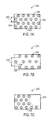
- FIG. 7A illustrates a typical pixel arrangement 200 for a transparent display 18 .
- each pixel 154 is enabled to emit a specific color of light.
- Each pixel 154 is labeled with an “R” for red emission, “G” for green emission, or “B” for blue emission.
- the display 18 may have a pixel arrangement with closely spaced pixels 154 , or a high pixel pitch.
- the pixel pitch is the distance between pixels 154 of the same color. For example, in FIG. 7A , the distance 202 between the red pixels is minimal, such that a maximum number of pixels 154 may be placed within the display 18 .
- FIG. 7B illustrates a modified pixel arrangement 210 useful for tuning the transparent regions 20 ( FIG. 1 ) of the display 18 by adjusting the spacing, or pitch of the pixels 154 .
- the pixels 154 are spaced at a greater distance 212 than those in FIG. 7A . While the resolution of the display 18 may decrease through less densely placed pixels 154 , the transparency of the display 18 may increase, thus providing a clearer view to or from components behind the display 18 .
- the increased pixel distances may be implemented in the entire display 18 or specific regions of the display 18 where increased transparency is desired.
- the display 18 may include regions where the pixel arrangement includes no pixels 154 .
- FIG. 7C illustrates one such embodiment of a pixel placement 220 , where a tuned region 222 contains no pixels 154 . Including one or more tuned regions 222 that do not have pixels 154 may enhance the transparency of such regions 222 by allowing light to freely pass through the layers of the display 18 .
- the tuned region 222 may be placed in areas of the display 18 where it may be less likely that a displayed image would be useful. For example, such tuned region 222 may be implemented at the edges and/or corners of the display 18 .
- Tuning transparency of a transparent display may result in enhanced usability of components placed behind the transparent display. Placing components that would typically be found on the surface of an electronic device enclosure behind a transparent display may increase the surface real-estate of the enclosure for a larger display or additional components. Further, the aesthetics of the electronic device may be greatly enhanced by not cluttering the device enclosure with always-visible components, but instead creating a more seamless electronic device where the components are only visible when they are in use.
Landscapes
- Engineering & Computer Science (AREA)
- Theoretical Computer Science (AREA)
- Physics & Mathematics (AREA)
- General Physics & Mathematics (AREA)
- General Engineering & Computer Science (AREA)
- Computer Hardware Design (AREA)
- Human Computer Interaction (AREA)
- Devices For Indicating Variable Information By Combining Individual Elements (AREA)
- Control Of Indicators Other Than Cathode Ray Tubes (AREA)
- Image Input (AREA)
Abstract
Systems, methods, and devices are disclosed for applying concealment of components of an electronic device. In one embodiment, an electronic device may include a component that is disposed behind a display (e.g., a transparent organic light-emitting diode (OLED) display) that is configured to selectively become transparent at certain transparency regions. Additionally, the electronic device includes data processing circuitry configured to determine when an event requesting that the component be exposed occurs. The data processing circuitry may control portions of the display to become transparent, to expose the component upon the occurrence of the event requesting that the component be exposed.
Description
This application is a continuation of patent application Ser. No. 13/308,119, filed on Nov. 30, 2011, which is hereby incorporated by reference herein in its entirety.
The present disclosure relates generally to the industrial design of an electronic device and, more particularly, to techniques for disposing components of an electronic device behind a transparent display, such as an organic light-emitting diode (OLED) display.
This section is intended to introduce the reader to various aspects of art that may be related to various aspects of the present techniques, which are described and/or claimed below. This discussion is believed to be helpful in providing the reader with background information to facilitate a better understanding of the various aspects of the present disclosure. Accordingly, it should be understood that these statements are to be read in this light, and not as admissions of prior art.
Electronic devices are becoming more and more sophisticated, capable of performing a multitude of tasks using a variety of components built into the electronic device. Providing increased functionality often involves adding components to such electronic devices. However, adding more components can lead to a cluttered, unattractive electronic device.
Current techniques for incorporating components into an electronic device may be limited by the relative sizes of the components and the electronic device. The larger the components and the smaller the electronic device, the less spatial area there may be to incorporate additional components. For example, a small electronic device where a large display covers most of the face of the electronic device may not allow for any additional components, such as a fingerprint reader, to be added to the electronic device. Furthermore, under the current techniques, adding new components may harm the aesthetic appeal of the device by cluttering the electronic device enclosure, even though these additional components may be seldom or never used by many users. An electronic device that incorporates multiple components may lose its aesthetic appeal when covered by visible components, particularly as compared to a seamless electronic device where very few, if any, components of the electronic device are visible.
A summary of certain embodiments disclosed herein is set forth below. It should be understood that these aspects are presented merely to provide the reader with a brief summary of these certain embodiments and that these aspects are not intended to limit the scope of this disclosure. Indeed, this disclosure may encompass a variety of aspects that may not be set forth below.
The present disclosure generally relates to techniques for disposing components of an electronic device behind a transparent display. Disposing the components behind the transparent display of the electronic device, may enable the components to remain hidden from view while not in use. When desired, the components of the electronic device may be exposed, allowing the components to suddenly appear as from out of nowhere. In accordance with one embodiment, an electronic device may include a transparent display with a component of the electronic device disposed behind the display. Upon detecting an event associated with the component, a processor of the electronic device may make transparent, or “open,” a transparent region (e.g., through generating a local or global black spot) of the display to expose the component. The black spot may be generated when pixels of the display are not emitting light in certain areas. To provide one example, such an event may occur when a feature of the electronic device requests exposure of concealed components. For example, when an image capture application of the electronic device is not in use, an image capture device and/or associated strobe may remain hidden behind the display of the electronic device. Upon detecting this request, the processor may open one or more transparent regions (e.g., generate black spots), causing the image capture device and/or the associated strobe to suddenly appear from behind the display.
Various refinements of the features noted above may exist in relation to various aspects of the present disclosure. Further features may also be incorporated in these various aspects as well. These refinements and additional features may exist individually or in any combination. For instance, various features discussed below in relation to one or more of the illustrated embodiments may be incorporated into any of the above-described aspects of the present disclosure alone or in any combination. Again, the brief summary presented above is intended only to familiarize the reader with certain aspects and contexts of embodiments of the present disclosure without limitation to the claimed subject matter.
Various aspects of this disclosure may be better understood upon reading the following detailed description and upon reference to the drawings in which:
One or more specific embodiments of the present disclosure will be described below. These described embodiments are only examples of the presently disclosed techniques. Additionally, in an effort to provide a concise description of these embodiments, all features of an actual implementation may not be described in the specification. It should be appreciated that in the development of any such actual implementation, as in any engineering or design project, numerous implementation-specific decisions must be made to achieve the developers' specific goals, such as compliance with system-related and business-related constraints, which may vary from one implementation to another. Moreover, it should be appreciated that such a development effort might be complex and time consuming, but would nevertheless be a routine undertaking of design, fabrication, and manufacture for those of ordinary skill having the benefit of this disclosure.
When introducing elements of various embodiments of the present disclosure, the articles “a,” “an,” and “the” are intended to mean that there are one or more of the elements. The terms “comprising,” “including,” and “having” are intended to be inclusive and mean that there may be additional elements other than the listed elements. Additionally, it should be understood that references to “one embodiment” or “an embodiment” of the present disclosure are not intended to be interpreted as excluding the existence of additional embodiments that also incorporate the recited features.
The present disclosure generally provides techniques for enhancing the functionality and aesthetic appeal of an electronic device by disposing components of the electronic device behind a display of the electronic device. To avoid cluttering the enclosure of an electronic device with various components, many different electronic device components may be disposed behind the display of the electronic device. Perhaps most noteworthy are components that, when functioning properly, have traditionally required external exposure to light or that emit light. For example, these “light-dependent components” may include an optical scanner (e.g., a biometric fingerprint scanner), an image capture device, a strobe, a light sensor, a proximity sensor, or a solar panel. Further, light-dependent components may include components that are configured to become visible when light is introduced, such as a printed image. Each of these components depend on light input or output light and thus have traditionally had at least a light input or light output portion of the component externally exposed when incorporated into an electronic device. Using the current techniques, these light-dependent components may be configured to be exposed from behind the display only when desired, and otherwise may remain hidden from view. These light-dependent components may remain hidden while the display is producing an image (e.g., emitting light) above the component and may become exposed when the display is not producing an image (e.g., emitting light) above the component.
Disposing components of an electronic device behind a display may provide an aesthetic benefit to the electronic device by allowing the components to remain unseen and hidden behind the display until access to the component is desired, creating a more seamless electronic device. Furthermore, the size of the display may increase because as components are disposed under the display, more surface real-estate of the device enclosure may become available. Additionally, because less surface real-estate may be needed to house the light-dependent components, in some embodiments, the electronic device may be reduced in size. Further, the aesthetic value may be greatly increased by allowing exposure to components from areas of the electronic device that a user would traditionally not expect.
With the foregoing in mind, a general description of suitable electronic devices for performing the presently disclosed techniques is provided below. In particular, FIG. 1 is a block diagram depicting various components that may be present in an electronic device suitable for use with the present techniques. FIG. 2 represents one example of a suitable electronic device, which may be, as illustrated, a handheld electronic device having a transparent display.
Turning first to FIG. 1 , an electronic device 10 for performing the presently disclosed techniques may include, among other things, one or more processors 12, memory 14, non-volatile storage 16, a display 18 with one or more transparent regions 20, image capture device(s) 22, an I/O interface 26, a network interface 28, input structures 30, a strobe 32, and a biometric sensor 34 (e.g., a fingerprint reader). As will be discussed further below, the transparent regions 20 of the display 18 may be disposed above certain of these components, such as image capture device(s) 22, a strobe 32, and/or an biometric sensor 34. The various functional blocks shown in FIG. 1 may include hardware elements (including circuitry), software elements (including computer code stored on a computer-readable medium) or a combination of both hardware and software elements. Further, FIG. 1 is only one example of a particular implementation and is merely intended to illustrate the types of components that may be present in the electronic device 10.
Before continuing, it should be understood that the system block diagram of the electronic device 10 shown in FIG. 1 is intended to be a high-level control diagram depicting various components that may be included in such an electronic device 10. That is, the illustrated connection lines between each individual component shown in FIG. 1 may not necessarily represent paths or directions through which data flows or is transmitted between various components of the electronic device 10. Indeed, as discussed below, the depicted processor(s) 12 may, in some embodiments, include multiple processors, such as a main processor (e.g., CPU), and dedicated image and/or video processors.
The processor(s) 12 and/or other data processing circuitry may be operably coupled with the memory 14 and the non-volatile storage 16 to perform various algorithms for carrying out the presently disclosed techniques. Such programs or instructions executed by the processor(s) 12 may be stored in any suitable manufacture that includes one or more tangible, computer-readable media at least collectively storing the instructions or routines, such as the memory 14 and the non-volatile storage 16. In example, non-volatile storage 16 may include ROM, CD-ROM, or RAM. Also, programs (e.g., an operating system) encoded on such memory 14 or non-volatile storage 16 may also include instructions that may be executed by the processor(s) 12 to enable the electronic device 10 to provide various functionalities, including those described herein.
The display 18 may be a touch-screen display that may enable users to interact with a graphical user interface of the electronic device 10. The display 18 may be any suitable type of transparent display, such as a transparent organic light-emitting diode (OLED) display, for example. Rather than clutter the electronic device 10, certain components of the electronic device 10 may be disposed behind the display 18. As will be described in more detail below, the display 18 includes one or more transparent regions 20 that define areas of transparency in the display 18. In some embodiments, the display 18 may include a global transparent region 20 that encompasses the entire viewable area of the display 18. In other embodiments, the display 18 may include one or more local transparent regions 20 that encompass only a portion of the viewable area of the display 18. Local transparent regions 20 may be tailored to any shape or size suitable for exposing one or more underlying components. For example, such components may be the image capture device(s) 22, the strobe 32, and/or the biometric sensor 34. In some embodiments, the components may include a solar panel, light sensor, proximity sensor, indicator light-emitting diodes (LEDs), alternative displays (e.g., E-Ink or other low powered displays), and/or reflective or colorful objects, such as an Apple logo, that becomes visible when light is introduced.
The image capture device(s) 22 may include a digital camera configured to acquire still and/or moving images (e.g., video). The image capture device(s) 22 may include a lens and one or more image sensors configured to capture and convert light into electrical signals. By way of example, the image sensor may include a CMOS image sensor (e.g., a CMOS active-pixel sensor (APS)) or a CCD (charge-coupled device) sensor. Generally, the image sensor in the image capture device(s) 22 may include an integrated circuit having an array of pixels, wherein each pixel includes a photodetector for sensing light from an image scene. The functionality of the image capture device(s) 22 may be enhanced by the use of a strobe 32. The strobe 32 may include a light-emitting diode (LED) light source configured to illuminate the subject of the image capture device(s) 22.
The biometric sensor 34, such as a fingerprint reader, may be configured to take an optical scan of a subject and compare the scanned image to a stored image. The stored image data may be retrieved from the memory 14 and/or non-volatile storage 16. Based on the scan by the biometric sensor 34, the electronic device 10 may verify the identity of the user. Identity verification may provide a more secure electronic purchase method as well as a more secure unlocking method for the electronic device 10.
The I/O interface 26 may enable the electronic device 10 to interface with various other electronic devices, as may the network interface 28. The network interface 28 may include, for example, an interface for a personal area network (PAN), such as a Bluetooth network, for a local area network (LAN), such as an 802.11x Wi-Fi network, and/or for a wide area network (WAN), such as a 3G or 4G cellular network.
The handheld device 36 may include an enclosure 38 to protect interior components from physical damage and to shield them from electromagnetic interference. Traditionally, many light-dependent components occupied surface space of the enclosure 38 external to the display 18. However, in the current embodiment various components are disposed behind the display 18, thus utilizing less surface real-estate of the enclosure 38. For example, the embodiment of FIG. 2 includes an image capture device 22, a strobe 32, a biometric sensor 34 in the form of a fingerprint reader, and an image 40 (e.g., reflective and/or colorful object) disposed behind local transparent regions 20 of the handheld device 36.
As depicted, the display 18 may provide a graphical user interface (GUI) 42 with icons 44 and a background image 46. When displayed without any black regions (e.g., regions where no light is emitted), the GUI 42 may mask the transparent regions 20, and thus the components 22, 32, 34, and 40 may not be visible. However, upon desired use of a component, the processor 12 (FIG. 1 ) may generate one or more local black regions by selectively disabling an emission of light over one or more of the transparent regions 20 above the component. Upon generating the black region, the component is exposed through the transparent region 20, and thus becomes visible.
Further, in certain embodiments, one or more components may become visible upon removing power from the handheld device 36. For example, FIGS. 3A and 3B illustrate an embodiment of a handheld device 36 where power is removed from the display 18. Similar to the embodiment of FIG. 2 , an image 40 is concealed behind the display 18 when the GUI 42 does not provide any black spots. Thus, as depicted in FIG. 3A , the image 40 is not visible while the display 18 emits light (e.g., provides a background image 46) over the image 40. However, as depicted in FIG. 3B , when the display 18 is powered-down, the light emitted over the image 40 may be reduced, such that the image 40 becomes visible through the display 18.
As noted above, the transparent display 18 may conceal a variety of components of the electronic device 10, such as the image capture device 22, the strobe 32, and/or a biometric sensor 34 such as a fingerprint reader, to name a few. To more clearly explain the component concealment process, a general description of such a process 110 will now be provided as depicted in FIG. 4 . The process 110 is intended to provide an initial high level overview of the concealment process, with more specific details of the process, including examples, being described further below.
The process 110 begins at block 112, when a component (e.g., image capture device(s) 22) is concealed behind a transparent display 18. For example, the component may be concealed by displaying an image (e.g., emitting light) on the transparent display 18 over the component. Next, at decision block 114, the electronic device 10 (e.g., processor 12 of FIG. 1 ) may detect whether an event associated with the component has occurred (e.g., a camera application is launched that will use a concealed image capture device 22). If no such event has occurred, the component may remain concealed behind the transparent display 18, and the process may flow to block 112. On the other hand, if such an event has occurred, the process may flow to block 116, and the electronic device 10 (e.g., processor 12) may open a transparent region 20 over the component (e.g., image capture device(s) 22) to expose the component. For example, to open the transparent region 20, the processor 12 may control the display 18 to stop emitting light over a region, creating a black spot (e.g., transparent region 20) in the display 18. At decision block 120, the electronic device 10 (e.g., processor 12) may detect whether the event associated with the component has completed. If not, the component may remain exposed. Once the electronic device 10 detects that the event is complete (e.g., the camera application is closed), in block 122, the electronic device 10 (e.g., processor 12) may close the transparent region 20, thus concealing the component.
An embodiment of the process 110 depicted in FIG. 4 is illustrated in FIG. 5 . In FIG. 5 , the handheld device 36 is shown to contain an image capture device 22 disposed behind transparent display 18. Upon selection of an image capture application by selecting the graphical user interface icon 44, the camera application is launched. The launching of the camera application may represent an event associated with the image capture device 22. Upon detection of such an event 130, the processor 12 of FIG. 1 may open the transparent region 20A over the image capture device 22. Thus, the image capture device 22 may be exposed, allowing images to be captured by the exposed image capture device 22. Further, additional transparent regions 20 may be opened to provide usability of other components. For example, in the current embodiment, the transparent region 20B over the strobe 32 may be opened to provide use of the strobe 32 as a flash for image capture. In some embodiments, the GUI 42 may emphasize the opened transparent regions 20 (e.g., 20A and 20B) by providing GUI 42 images notifying a user of the opened transparent regions 20. For example, in the depicted embodiment, the GUI 42 provides a camera image 132 around the image capture device 22 and the strobe 32, illustrating the locations of the image capture device 22 and the strobe 32.
Turning now to a discussion of creating the transparent regions 20, FIG. 6 illustrates a cross-sectional view of the layers present in a particular embodiment of the display 18. In this embodiment, the display 18 includes an OLED panel 150. The OLED panel 150 includes a substrate layer 152 (e.g., a glass substrate layer) on which a thin film transistor (TFT) layer may be formed. The TFT layer may define the various pixels 154 of the OLED display and allow each pixel 154 to be separately addressed. In one embodiment, each pixel 154 may include a layer or layers of organic light-emitting diodes 156 printed, deposited, or otherwise formed on the substrate layer 152 and the TFT layer. Each of the light-emitting diodes 156 may emit specific colors (e.g., red, green, and blue) such that their color combined with other light-emitting diodes 156 may form a color image. In alternative embodiments, the light-emitting diodes 156 may each emit white and a color filter may transform the white light into specific colors (e.g., red, green, and blue). The operation of the TFT layer and the corresponding pixels 154 of the OLED panel 150 may be coordinated and/or controlled by one or more driver chips 158 (such as a chip-on glass (COG)) in communication with the TFT layer and/or the one or more processors 12 (FIG. 1 ).
As previously discussed, the transparent regions 20 may be formed when a transparent display 18 is not emitting light in certain regions. For example, the pixels 154 may be transparent, enabling light to pass through them such that components behind the pixels may be seen when the pixels 154 are not emitting light. However, when the pixels 154 are emitting light, the pixels 154 may not allow light to pass through them, and thus the components behind the pixels 154 may not be seen. Because the pixels 154 may be separately addressed, the driver chips 158 and/or processor(s) 12 (FIG. 1 ) may control any combination of pixels 154 to stop emitting light, thus allowing for transparent regions (e.g., black spots) of numerous sizes and/or shapes to be formed.
The OLED panel 150 may also include a circular polarizer layer 160. The circular polarizer layer 160 may absorb a significant amount of the reflected light from the OLED panel 150. Further, the OLED panel 150 may also include a cover or external layer 162 (e.g., a cover glass) that forms the external viewing surface facing a viewer. In certain embodiments the cover layer 162 may perform various color filtration and/or polarization functions with respect to the light emitted by the OLED panel 150. In one embodiment, the cover layer 162 and the substrate layer 152 may be bonded together, such as by a glass frit bond 164, along all or part of the periphery of the surface and/or substrate layers. In one implementation, the OLED panel 150 is between about 1.5 mm and 1.9 mm in thickness.
The background layer 166 may be provided as a single or multiple layer structure of a solid color (e.g., white) or printed background. For example, in one embodiment the background layer 166 includes a transflective layer 168 positioned over a solid-color substrate layer 170, such as a white substrate layer. The transflective layer 168 acts to both reflect ambient light and to transmit the color, image, and/or pattern of the substrate layer 170. In one implementation, the background layer 166 is between about 0.5 mm and 1.0 mm in thickness.
As discussed above with regards to FIGS. 3A and 3B , it may be desirable to provide a printed image 40. As an alternative to the embodiment depicted in FIGS. 3A and 3B , where the printed image 40 is present behind the display 18, in certain embodiments, the display 18 may contain the printed image 40. In such embodiments, the substrate layer 170 may incorporate the printed image 40 (e.g., a corporate logo, emblem, name, or mark). The printed image 40, such as a logo, may not be visible when the display 18 is emitting light and thus not in a transparent state. However, when a black region is formed over the printed image 40 or the display 18 is powered off and, thus, not emitting light, the printed image 40 (e.g., the logo, emblem, or mark) present on or visible through the substrate layer 170 may become visible.
It may be desirable to tune the transparency of display 18, such that components 172 behind the display 18 may be more clearly visible through the transparent regions 20. By locally removing portions 174 of the circular polarizer layer 160, the transparency of the OLED panel 150 may be tuned to more clearly expose components 172. For example, light that would typically be absorbed by the circular polarizer layer 160 may reflect off of the components 172, thus illuminating them. Further, as illustrated in the depicted embodiment, transparent regions 20 may be formed by cutting out portions 176 of the background layer 166 such that components 172 positioned behind the background layer 166 may be visible when the display 18 is not emitting an image over the cut out portions 176. In alternative embodiments, the entire background layer 166 may be removed, thus providing a global transparent region 20.
The transparency of the display 18 may also be tuned by modifying the pixel arrangement of the OLED panel 150. While the pixels 154 may be substantially transparent (e.g., 85% transparent), they may not be completely transparent. Thus, reducing the density of the pixels 154 may increase the transparency of the display 18 by creating light pathways in between the pixels 154. FIG. 7A illustrates a typical pixel arrangement 200 for a transparent display 18. In the depicted embodiment, each pixel 154 is enabled to emit a specific color of light. Each pixel 154 is labeled with an “R” for red emission, “G” for green emission, or “B” for blue emission. Typically, the display 18 may have a pixel arrangement with closely spaced pixels 154, or a high pixel pitch. The pixel pitch is the distance between pixels 154 of the same color. For example, in FIG. 7A , the distance 202 between the red pixels is minimal, such that a maximum number of pixels 154 may be placed within the display 18.
By decreasing the density of the pixels 154, the transparency of the display 18 may be increased. FIG. 7B illustrates a modified pixel arrangement 210 useful for tuning the transparent regions 20 (FIG. 1 ) of the display 18 by adjusting the spacing, or pitch of the pixels 154. As illustrated, the pixels 154 are spaced at a greater distance 212 than those in FIG. 7A . While the resolution of the display 18 may decrease through less densely placed pixels 154, the transparency of the display 18 may increase, thus providing a clearer view to or from components behind the display 18.
The increased pixel distances (e.g., decreased pixel density) may be implemented in the entire display 18 or specific regions of the display 18 where increased transparency is desired. In some embodiments, the display 18 may include regions where the pixel arrangement includes no pixels 154. For example, FIG. 7C illustrates one such embodiment of a pixel placement 220, where a tuned region 222 contains no pixels 154. Including one or more tuned regions 222 that do not have pixels 154 may enhance the transparency of such regions 222 by allowing light to freely pass through the layers of the display 18. In some embodiments, the tuned region 222 may be placed in areas of the display 18 where it may be less likely that a displayed image would be useful. For example, such tuned region 222 may be implemented at the edges and/or corners of the display 18.
Tuning transparency of a transparent display may result in enhanced usability of components placed behind the transparent display. Placing components that would typically be found on the surface of an electronic device enclosure behind a transparent display may increase the surface real-estate of the enclosure for a larger display or additional components. Further, the aesthetics of the electronic device may be greatly enhanced by not cluttering the device enclosure with always-visible components, but instead creating a more seamless electronic device where the components are only visible when they are in use.
The specific embodiments described above have been shown by way of example, and it should be understood that these embodiments may be susceptible to various modifications and alternative forms. It should be further understood that the claims are not intended to be limited to the particular forms disclosed, but rather to cover all modifications, equivalents, and alternatives falling within the spirit and scope of this disclosure.
Claims (18)
1. An electronic device comprising:
a display having a substrate and having an array of pixels on the substrate;
a component behind the substrate; and
processing circuitry that selectively controls the array of pixels to generate a transparent region and an adjacent non-transparent region on the display, wherein the transparent region overlaps the component and wherein the processing circuitry is configured to alter a shape of the transparent region.
2. The electronic device defined in claim 1 wherein the component is selected from the group consisting of: a light sensor, a biometric sensor, a solar panel, a light-emitting diode, and a reflective image.
3. The electronic device defined in claim 1 wherein the transparent region includes a first portion of the array of pixels that is not emitting light and the non-transparent region includes a second portion of the array of pixels that is emitting light.
4. The electronic device defined in claim 3 wherein the first portion of the array of pixels has a lower pixel density than the second portion of the array of pixels.
5. The electronic device defined in claim 1 wherein display produces images in the non-transparent region.
6. The electronic device defined in claim 1 wherein the component comprises a light sensor that receives light through the transparent region.
7. The electronic device defined in claim 1 further comprising an additional component behind the substrate, wherein the processing circuitry selectively controls the array of pixels to generate an additional transparent region over the additional component.
8. The electronic device defined in claim 1 wherein the pixels comprise organic light-emitting diode pixels.
9. The electronic device defined in claim 1 wherein the display comprises a polarizer having an opening that overlaps the component.
10. An electronic device, comprising:
an organic light-emitting diode display having a substrate, an array of thin-film transistors on the substrate, and a touch sensor that receives touch input;
a light sensor behind the substrate; and
processing circuitry that controls the array of thin-film transistors to produce a transparent region in the organic light-emitting diode display in response to the touch input, wherein the light sensor receives light through the transparent region.
11. The electronic device defined in claim 10 wherein the light sensor comprises a light sensor selected from the group consisting of: an image sensor and a fingerprint reader.
12. The electronic device defined in claim 10 wherein the processing circuitry controls the array of thin-film transistors to produce images adjacent to the transparent region.
13. The electronic device defined in claim 10 wherein the processing circuitry controls the array of thin-film transistors to transition the transparent region from a transparent state to a non-transparent state.
14. The electronic device defined in claim 10 wherein the light sensor comprises a camera, wherein the organic light-emitting diode display produces an image of a camera icon, and wherein the processing circuitry controls the array of thin-film transistors to produce the transparent region in response to touch input at the camera icon.
15. An electronic device comprising:
a display having an array of pixels on a display substrate and having a touch sensor that receives touch input;
components behind the display substrate, wherein the components comprise a light source; and
processing circuitry that controls the array of pixels to produce transparent regions on the display to expose the components, wherein each transparent region overlaps a respective one of the components, and wherein the processing circuitry determines which component to expose based on the touch input.
16. The electronic device defined in claim 15 wherein the components comprise a light sensor.
17. An electronic device comprising:
a display having an array of pixels on a display substrate and having a touch sensor that receives touch input, wherein the display substrate comprises glass;
components behind the display substrate; and
processing circuitry that controls the array of pixels to produce transparent regions on the display to expose the components, wherein each transparent region overlaps a respective one of the components, and wherein the processing circuitry determines which component to expose based on the touch input.
18. The electronic device defined in claim 17 wherein the pixels comprise organic light-emitting diode pixels.
Priority Applications (3)
| Application Number | Priority Date | Filing Date | Title |
|---|---|---|---|
| US15/240,472 US10019940B2 (en) | 2011-11-30 | 2016-08-18 | Devices and methods for providing access to internal component |
| US16/029,395 US11074855B2 (en) | 2011-11-30 | 2018-07-06 | Devices and methods for providing access to internal component |
| US17/377,198 US20210343235A1 (en) | 2011-11-30 | 2021-07-15 | Devices and methods for providing access to internal component |
Applications Claiming Priority (2)
| Application Number | Priority Date | Filing Date | Title |
|---|---|---|---|
| US13/308,119 US9437132B2 (en) | 2011-11-30 | 2011-11-30 | Devices and methods for providing access to internal component |
| US15/240,472 US10019940B2 (en) | 2011-11-30 | 2016-08-18 | Devices and methods for providing access to internal component |
Related Parent Applications (1)
| Application Number | Title | Priority Date | Filing Date |
|---|---|---|---|
| US13/308,119 Continuation US9437132B2 (en) | 2011-11-30 | 2011-11-30 | Devices and methods for providing access to internal component |
Related Child Applications (1)
| Application Number | Title | Priority Date | Filing Date |
|---|---|---|---|
| US16/029,395 Continuation US11074855B2 (en) | 2011-11-30 | 2018-07-06 | Devices and methods for providing access to internal component |
Publications (2)
| Publication Number | Publication Date |
|---|---|
| US20160358543A1 US20160358543A1 (en) | 2016-12-08 |
| US10019940B2 true US10019940B2 (en) | 2018-07-10 |
Family
ID=48466430
Family Applications (4)
| Application Number | Title | Priority Date | Filing Date |
|---|---|---|---|
| US13/308,119 Active 2034-05-01 US9437132B2 (en) | 2011-11-30 | 2011-11-30 | Devices and methods for providing access to internal component |
| US15/240,472 Active US10019940B2 (en) | 2011-11-30 | 2016-08-18 | Devices and methods for providing access to internal component |
| US16/029,395 Active 2032-08-18 US11074855B2 (en) | 2011-11-30 | 2018-07-06 | Devices and methods for providing access to internal component |
| US17/377,198 Pending US20210343235A1 (en) | 2011-11-30 | 2021-07-15 | Devices and methods for providing access to internal component |
Family Applications Before (1)
| Application Number | Title | Priority Date | Filing Date |
|---|---|---|---|
| US13/308,119 Active 2034-05-01 US9437132B2 (en) | 2011-11-30 | 2011-11-30 | Devices and methods for providing access to internal component |
Family Applications After (2)
| Application Number | Title | Priority Date | Filing Date |
|---|---|---|---|
| US16/029,395 Active 2032-08-18 US11074855B2 (en) | 2011-11-30 | 2018-07-06 | Devices and methods for providing access to internal component |
| US17/377,198 Pending US20210343235A1 (en) | 2011-11-30 | 2021-07-15 | Devices and methods for providing access to internal component |
Country Status (1)
| Country | Link |
|---|---|
| US (4) | US9437132B2 (en) |
Cited By (5)
| Publication number | Priority date | Publication date | Assignee | Title |
|---|---|---|---|---|
| US11281035B2 (en) | 2019-04-23 | 2022-03-22 | Samsung Electronics Co., Ltd. | Display and electronic device including the same |
| US11601537B2 (en) | 2020-06-04 | 2023-03-07 | Samsung Electronics Co., Ltd. | Electronic device including display |
| US11895383B2 (en) | 2021-01-27 | 2024-02-06 | Samsung Electronics Co., Ltd. | Electronic device including optical sensor |
| US12395580B2 (en) | 2020-08-28 | 2025-08-19 | Google Llc | OLED display module structure for mitigating dark spot visibility in back cover open regions |
| US12406613B2 (en) | 2021-08-10 | 2025-09-02 | Samsung Electronics Co., Ltd. | Electronic device including display and camera and method controlling thereof |
Families Citing this family (93)
| Publication number | Priority date | Publication date | Assignee | Title |
|---|---|---|---|---|
| US9313858B2 (en) * | 2011-06-10 | 2016-04-12 | Koninklijke Philips N.V. | Phosphor enhanced light source for presenting a visible pattern and a luminaire |
| KR20130064486A (en) * | 2011-12-08 | 2013-06-18 | 삼성디스플레이 주식회사 | Display device |
| US20130231157A1 (en) * | 2012-03-02 | 2013-09-05 | Jeffrey Chung | Cellular phone with camera at front edge area |
| US9385172B2 (en) | 2012-10-19 | 2016-07-05 | Universal Display Corporation | One-way transparent display |
| US9384691B2 (en) | 2012-10-19 | 2016-07-05 | Universal Display Corporation | Transparent display and illumination device |
| US9385340B2 (en) * | 2012-10-19 | 2016-07-05 | Universal Display Corporation | Transparent display and illumination device |
| WO2014097315A2 (en) * | 2012-12-17 | 2014-06-26 | Balakrishna Anil Kumar | Display apparatus |
| KR20140092119A (en) * | 2013-01-15 | 2014-07-23 | 삼성디스플레이 주식회사 | Flat panel display device |
| US9772712B2 (en) | 2014-03-11 | 2017-09-26 | Textron Innovations, Inc. | Touch screen instrument panel |
| US10005562B2 (en) * | 2014-03-11 | 2018-06-26 | Textron Innovations Inc. | Standby instrument panel for aircraft |
| CN105094402B (en) * | 2014-05-15 | 2018-06-12 | 宸鸿科技(厦门)有限公司 | Touch control display device |
| KR102333868B1 (en) * | 2014-12-10 | 2021-12-07 | 엘지디스플레이 주식회사 | Organic light emitting diode display device |
| US10147757B2 (en) | 2015-02-02 | 2018-12-04 | Synaptics Incorporated | Image sensor structures for fingerprint sensing |
| US10181070B2 (en) | 2015-02-02 | 2019-01-15 | Synaptics Incorporated | Low profile illumination in an optical fingerprint sensor |
| US9829614B2 (en) | 2015-02-02 | 2017-11-28 | Synaptics Incorporated | Optical sensor using collimator |
| US10243162B2 (en) | 2015-06-17 | 2019-03-26 | Universal Display Corporation | Close illumination system |
| US20170084231A1 (en) * | 2015-09-23 | 2017-03-23 | Intel Corporation | Imaging system management for camera mounted behind transparent display |
| US9762781B2 (en) | 2015-10-30 | 2017-09-12 | Essential Products, Inc. | Apparatus and method to maximize the display area of a mobile device by increasing the size of the display without necessarily increasing the size of the phone |
| US9767728B2 (en) | 2015-10-30 | 2017-09-19 | Essential Products, Inc. | Light sensor beneath a dual-mode display |
| US9864400B2 (en) | 2015-10-30 | 2018-01-09 | Essential Products, Inc. | Camera integrated into a display |
| US9823694B2 (en) | 2015-10-30 | 2017-11-21 | Essential Products, Inc. | Camera integrated into a display |
| US9870024B2 (en) | 2015-10-30 | 2018-01-16 | Essential Products, Inc. | Camera integrated into a display |
| US9525764B1 (en) | 2015-10-30 | 2016-12-20 | Essential Products, Inc. | Co-mold features on a chassis shell of a mobile device |
| US9754526B2 (en) * | 2015-10-30 | 2017-09-05 | Essential Products, Inc. | Mobile device with display overlaid with at least a light sensor |
| US10102789B2 (en) | 2015-10-30 | 2018-10-16 | Essential Products, Inc. | Mobile device with display overlaid with at least a light sensor |
| US9736383B2 (en) * | 2015-10-30 | 2017-08-15 | Essential Products, Inc. | Apparatus and method to maximize the display area of a mobile device |
| US10331260B2 (en) * | 2015-10-30 | 2019-06-25 | Essential Products, Inc. | Variable transparency layers for electronic devices |
| KR102419624B1 (en) | 2016-01-21 | 2022-07-11 | 삼성전자 주식회사 | Arrangement structure of sensor of electronic apparatus |
| US10229316B2 (en) | 2016-01-29 | 2019-03-12 | Synaptics Incorporated | Compound collimating system using apertures and collimators |
| US9843736B2 (en) | 2016-02-26 | 2017-12-12 | Essential Products, Inc. | Image capture with a camera integrated display |
| WO2017164680A1 (en) * | 2016-03-24 | 2017-09-28 | 삼성전자주식회사 | Electronic device having display |
| US9961178B2 (en) * | 2016-03-24 | 2018-05-01 | Motorola Mobility Llc | Embedded active matrix organic light emitting diode (AMOLED) fingerprint sensor |
| KR20170113066A (en) * | 2016-03-24 | 2017-10-12 | 삼성전자주식회사 | Electronic device with display and method for displaying image thereof |
| KR102373566B1 (en) | 2016-09-23 | 2022-03-14 | 삼성디스플레이 주식회사 | Display device |
| US20180114493A1 (en) * | 2016-10-21 | 2018-04-26 | Motorola Mobility Llc | Electronic Device with Display-Based Image Compensation and Corresponding Systems and Methods |
| CN106775390A (en) * | 2016-11-30 | 2017-05-31 | 努比亚技术有限公司 | Rimless terminal and unlocking method |
| US10055637B2 (en) | 2016-12-07 | 2018-08-21 | Synaptics Incorporated | Optical sensor with substrate light filter |
| KR102566717B1 (en) | 2016-12-12 | 2023-08-14 | 삼성전자 주식회사 | Electronic device having a biometric sensor |
| KR102567543B1 (en) * | 2017-01-06 | 2023-08-21 | 삼성전자 주식회사 | Electronic device and method to control display unit for sensing a biometric sensor |
| GB201700530D0 (en) * | 2017-01-12 | 2017-03-01 | Purelifi Ltd | Display apparatus |
| CN106878564A (en) * | 2017-03-07 | 2017-06-20 | 广东欧珀移动通信有限公司 | Display control method and device, display screen and mobile terminal |
| CN111314521A (en) * | 2017-03-07 | 2020-06-19 | Oppo广东移动通信有限公司 | Terminal device |
| US11422662B2 (en) * | 2017-06-14 | 2022-08-23 | Samsung Electronics Co., Ltd. | Electronic device including light emitting module and light receiving module adjacent to display, and operating method thereof |
| CN110024366B (en) * | 2017-07-07 | 2020-08-14 | 华为技术有限公司 | A terminal with a camera and a shooting method |
| KR102452251B1 (en) | 2017-08-04 | 2022-10-11 | 삼성디스플레이 주식회사 | Display apparatus |
| CN109445883A (en) * | 2017-08-31 | 2019-03-08 | 北京嘀嘀无限科技发展有限公司 | Interface display system and method |
| WO2019062221A1 (en) | 2017-09-30 | 2019-04-04 | 云谷(固安)科技有限公司 | Display screen and display device |
| CN108171178A (en) * | 2017-12-29 | 2018-06-15 | 昆山国显光电有限公司 | A kind of method for controlling fingerprint identification and touch panel, display device |
| KR102413113B1 (en) * | 2018-01-08 | 2022-06-27 | 삼성전자주식회사 | An electronic device comprising a sensor for generating image data using incident light through an opening formed in a display |
| US10690973B2 (en) | 2018-01-19 | 2020-06-23 | Innolux Corporation | Electronic device |
| CN110134182A (en) * | 2018-02-08 | 2019-08-16 | 深圳富泰宏精密工业有限公司 | Portable electronic device and its operating method |
| CN108254963A (en) * | 2018-03-20 | 2018-07-06 | 京东方科技集团股份有限公司 | A kind of display panel, display module, display device and its driving method |
| US11073712B2 (en) * | 2018-04-10 | 2021-07-27 | Apple Inc. | Electronic device display for through-display imaging |
| KR102668689B1 (en) * | 2018-05-10 | 2024-05-24 | 삼성디스플레이 주식회사 | Display apparatus and Manufacturing method thereof |
| CN108810201B (en) * | 2018-06-04 | 2020-07-17 | Oppo广东移动通信有限公司 | Electronic device and method for taking photo by using same |
| US10598838B2 (en) * | 2018-06-29 | 2020-03-24 | Intel Corporation | Pixel level polarizer for flexible display panels |
| CN109104510A (en) * | 2018-08-31 | 2018-12-28 | 武汉华星光电技术有限公司 | Display device and display methods |
| CN109116656B (en) * | 2018-09-03 | 2021-06-29 | Oppo广东移动通信有限公司 | Electronic device, electrochromic portion control method, and storage medium |
| KR102578096B1 (en) * | 2018-09-21 | 2023-09-14 | 삼성전자주식회사 | Electronic device for improving visual recognition of partial area of display |
| KR102697258B1 (en) | 2018-09-27 | 2024-08-21 | 삼성디스플레이 주식회사 | Display device |
| CN110969982B (en) | 2018-09-28 | 2022-09-13 | 北京小米移动软件有限公司 | Display structure, display panel and display device |
| KR102622046B1 (en) | 2018-10-11 | 2024-01-09 | 삼성디스플레이 주식회사 | Display device |
| KR102752761B1 (en) | 2018-10-26 | 2025-01-09 | 삼성디스플레이 주식회사 | Display device |
| CN109542564A (en) * | 2018-11-12 | 2019-03-29 | 广州华多网络科技有限公司 | View steering method, device, computer readable storage medium and computer equipment |
| CN109547598B (en) * | 2018-11-30 | 2020-06-26 | Oppo广东移动通信有限公司 | Camera module control method and device |
| KR102656932B1 (en) * | 2018-12-28 | 2024-04-11 | 엘지디스플레이 주식회사 | Display apparatus including transmissive light source |
| CN111385406A (en) * | 2018-12-28 | 2020-07-07 | 武汉华星光电半导体显示技术有限公司 | Electronic equipment, control method of screen of electronic equipment and storage medium |
| CN109714532A (en) * | 2018-12-29 | 2019-05-03 | 联想(北京)有限公司 | Image-pickup method, treating method and apparatus |
| CN111435185B (en) * | 2019-01-11 | 2025-12-30 | 北京小米移动软件有限公司 | Polarizing film, display screen, terminal and manufacturing method of polarizing film |
| CN110767157B (en) | 2019-01-31 | 2020-11-06 | 昆山国显光电有限公司 | Display device, display panel thereof, and OLED array substrate |
| CN109919845A (en) * | 2019-03-08 | 2019-06-21 | 武汉华星光电技术有限公司 | With aperture display image treatment method in screen |
| CN110288946B (en) * | 2019-06-25 | 2021-10-15 | 荣耀终端有限公司 | Mobile terminal and driving method thereof, display module, and driving chip |
| KR102914150B1 (en) * | 2019-06-26 | 2026-01-16 | 삼성디스플레이 주식회사 | Display device |
| US11871635B2 (en) | 2019-06-28 | 2024-01-09 | Samsung Display Co., Ltd. | Display panel and display device |
| GB2585692A (en) | 2019-07-12 | 2021-01-20 | Continental Automotive Gmbh | A method of embedding an imaging device within a display |
| KR20210012086A (en) * | 2019-07-23 | 2021-02-03 | 삼성디스플레이 주식회사 | Display device |
| CN110381189A (en) * | 2019-08-12 | 2019-10-25 | Oppo广东移动通信有限公司 | Battery, camera module and electronic equipment |
| KR102859922B1 (en) | 2019-09-03 | 2025-09-15 | 삼성디스플레이 주식회사 | Display device |
| CN112748894B (en) * | 2019-10-30 | 2025-08-05 | 北京小米移动软件有限公司 | Hole-punch screen display method and device |
| CN111049973B (en) * | 2019-11-22 | 2021-06-01 | 维沃移动通信有限公司 | A screen display control method, electronic device and computer-readable storage medium |
| KR20210078638A (en) | 2019-12-18 | 2021-06-29 | 삼성디스플레이 주식회사 | Display apparatus and the Manufacturing method thereof |
| CN111292628B (en) * | 2020-02-14 | 2022-02-22 | 维沃移动通信有限公司 | Display screen and electronic equipment |
| KR102838512B1 (en) * | 2020-02-14 | 2025-07-28 | 삼성디스플레이 주식회사 | Display device |
| US12207516B2 (en) | 2020-02-14 | 2025-01-21 | Samsung Display Co., Ltd. | Organic light-emitting display device |
| KR20220014371A (en) * | 2020-07-23 | 2022-02-07 | 삼성디스플레이 주식회사 | Display device and method for fabricating the same |
| EP4001989B1 (en) * | 2020-11-12 | 2025-07-09 | Infineon Technologies AG | Electronic device and method for an electronic device |
| EP4002813B1 (en) * | 2020-11-12 | 2024-10-09 | Infineon Technologies AG | Sensor positioned behind a micro-led area within an oled display |
| EP4001957B1 (en) | 2020-11-12 | 2023-03-01 | Infineon Technologies AG | Electronic device with display-integrated illumination element and corresponding control method |
| KR102876468B1 (en) | 2021-03-23 | 2025-10-27 | 삼성디스플레이 주식회사 | Display device |
| US11619857B2 (en) | 2021-05-25 | 2023-04-04 | Apple Inc. | Electrically-tunable optical filter |
| KR20230009636A (en) * | 2021-07-09 | 2023-01-17 | 삼성전자주식회사 | Electronic device, and operating method of electronic device |
| US12114089B2 (en) | 2022-08-19 | 2024-10-08 | Apple Inc. | Pixel output parasitic capacitance reduction and predictive settling assist |
| US12550517B2 (en) | 2022-09-22 | 2026-02-10 | Apple Inc. | Same focal plane pixel design for RGB-IR image sensors |
Citations (29)
| Publication number | Priority date | Publication date | Assignee | Title |
|---|---|---|---|---|
| US5349174A (en) * | 1992-05-06 | 1994-09-20 | U.S. Philips Corporation | Image sensor with transparent capacitive regions |
| US20020021561A1 (en) * | 2000-06-30 | 2002-02-21 | Hiroshi Yamauchi | Aggregate of electronic components and mounting method thereof |
| US20020167809A1 (en) | 2001-05-09 | 2002-11-14 | Glass Philip John | Louvered screen to control light |
| US20020196517A1 (en) * | 2001-06-05 | 2002-12-26 | Seiko Epson Corporation | Electro-optical device, electronic apparatus, and method for manufacturing electro-optical device |
| US20030016189A1 (en) | 2001-07-10 | 2003-01-23 | Naoto Abe | Display driving method and display apparatus utilizing the same |
| US20030067424A1 (en) | 2001-10-10 | 2003-04-10 | Hajime Akimoto | Image display device |
| US20030081158A1 (en) | 2001-10-31 | 2003-05-01 | Zili Li | Display and solar cell device |
| US20040263670A1 (en) | 2003-06-18 | 2004-12-30 | Ryo Yamasaki | Display device with image sensing device |
| US20050083269A1 (en) | 2003-10-21 | 2005-04-21 | Yu-Hsiang Lin | [driving method of improving brightness uniformity of oled/pled display] |
| US20050200293A1 (en) * | 2004-02-24 | 2005-09-15 | Naugler W. E.Jr. | Penlight and touch screen data input system and method for flat panel displays |
| US20050200291A1 (en) | 2004-02-24 | 2005-09-15 | Naugler W. E.Jr. | Method and device for reading display pixel emission and ambient luminance levels |
| US20080018555A1 (en) | 2006-07-21 | 2008-01-24 | Huei Pei Kuo | See-through display |
| US20080128728A1 (en) | 2004-09-10 | 2008-06-05 | Luminus Devices, Inc. | Polarized light-emitting devices and methods |
| US20080309633A1 (en) * | 2007-06-13 | 2008-12-18 | Apple Inc. | Touch-sensitive display |
| US20090015761A1 (en) | 2007-05-04 | 2009-01-15 | Itronix Corporation | Combination transparent touch panel liquid crystal display stack and methods of manufacturing same |
| US7495927B2 (en) * | 2007-01-24 | 2009-02-24 | Epson Imaging Devices Corporation | Mount structure, electro-optical device, and electronic apparatus |
| US7495895B2 (en) | 2006-04-19 | 2009-02-24 | Carnevali Jeffrey D | Protective cover for device having touch screen |
| US20090102763A1 (en) | 2007-10-19 | 2009-04-23 | Border John N | Display device with capture capabilities |
| US20090184936A1 (en) | 2008-01-22 | 2009-07-23 | Mathematical Inventing - Slicon Valley | 3D touchpad |
| US7697053B2 (en) | 2006-11-02 | 2010-04-13 | Eastman Kodak Company | Integrated display having multiple capture devices |
| US20100138763A1 (en) * | 2008-12-01 | 2010-06-03 | Lg Electronics Inc. | Method for operating execution icon of mobile terminal |
| US20100245741A1 (en) | 2009-03-30 | 2010-09-30 | Infovision Optoelectronics (Kunshan) Co., Ltd. | Liquid Crystal Display Panel, Liquid Crystal Display Apparatus and Manufacturing Method Thereof |
| US20100283762A1 (en) * | 2008-03-31 | 2010-11-11 | Yasunobu Takusa | Display device, electronic equipment provided with the display device, and touch panel |
| US8176437B1 (en) | 2011-07-18 | 2012-05-08 | Google Inc. | Responsiveness for application launch |
| US20120148115A1 (en) | 2006-08-11 | 2012-06-14 | Birdwell J Douglas | Mobile Biometrics Information Collection and Identification |
| US8203546B2 (en) * | 2007-02-07 | 2012-06-19 | Plastic Logic Limited | Electronic document reading devices |
| US8384690B2 (en) | 2010-05-14 | 2013-02-26 | International Business Machines Corp. | Interface device with integrated solar cell(S) for power collection |
| US8467177B2 (en) | 2010-10-29 | 2013-06-18 | Apple Inc. | Displays with polarizer windows and opaque masking layers for electronic devices |
| US8633916B2 (en) | 2009-12-10 | 2014-01-21 | Apple, Inc. | Touch pad with force sensors and actuator feedback |
Family Cites Families (20)
| Publication number | Priority date | Publication date | Assignee | Title |
|---|---|---|---|---|
| US5159445A (en) * | 1990-12-31 | 1992-10-27 | At&T Bell Laboratories | Teleconferencing video display system for improving eye contact |
| US20040233038A1 (en) * | 2001-07-10 | 2004-11-25 | American Express Travel Related Services Company, Inc. | Method and system for retinal scan recognition biometrics on a fob |
| US7728906B2 (en) * | 2006-01-04 | 2010-06-01 | Apple Inc. | Embedded camera with privacy filter |
| US7808540B2 (en) * | 2007-01-09 | 2010-10-05 | Eastman Kodak Company | Image capture and integrated display apparatus |
| JP4978224B2 (en) * | 2007-02-08 | 2012-07-18 | カシオ計算機株式会社 | Photoelectric conversion device and display panel having the same |
| TW200912720A (en) * | 2007-04-24 | 2009-03-16 | White Electronics Designs Corp | Interactive display system |
| US9195329B2 (en) * | 2007-05-04 | 2015-11-24 | Blackberry Limited | Touch-sensitive device |
| JP5014439B2 (en) * | 2007-12-20 | 2012-08-29 | シャープ株式会社 | Display device with optical sensor |
| US20090322706A1 (en) * | 2008-06-26 | 2009-12-31 | Symbol Technologies, Inc. | Information display with optical data capture |
| KR101544364B1 (en) * | 2009-01-23 | 2015-08-17 | 삼성전자주식회사 | Mobile terminal having dual touch screen and method for controlling contents thereof |
| KR101563523B1 (en) * | 2009-01-30 | 2015-10-28 | 삼성전자주식회사 | Mobile terminal having dual touch screen and method for displaying user interface thereof |
| US8217913B2 (en) * | 2009-02-02 | 2012-07-10 | Apple Inc. | Integrated touch screen |
| JP2012027511A (en) * | 2009-04-23 | 2012-02-09 | Univ Of Tsukuba | Input device |
| US8008613B2 (en) * | 2009-05-05 | 2011-08-30 | Apple Inc. | Light sensing device having a color sensor and a clear sensor for infrared rejection |
| TWI404994B (en) * | 2009-12-14 | 2013-08-11 | Wintek Corp | Touch panel |
| US9143668B2 (en) * | 2010-10-29 | 2015-09-22 | Apple Inc. | Camera lens structures and display structures for electronic devices |
| US20120257004A1 (en) * | 2011-04-05 | 2012-10-11 | Polycom, Inc. | Direct Eye-Contact Enhancing Videoconferencing Unit |
| KR20130057700A (en) * | 2011-11-24 | 2013-06-03 | 삼성디스플레이 주식회사 | Organic light emitting device |
| KR102080741B1 (en) * | 2012-08-29 | 2020-02-24 | 엘지전자 주식회사 | Mobile terminal and control method thereof |
| TWI772621B (en) * | 2019-03-08 | 2022-08-01 | 聚積科技股份有限公司 | On-screen sensing control method |
-
2011
- 2011-11-30 US US13/308,119 patent/US9437132B2/en active Active
-
2016
- 2016-08-18 US US15/240,472 patent/US10019940B2/en active Active
-
2018
- 2018-07-06 US US16/029,395 patent/US11074855B2/en active Active
-
2021
- 2021-07-15 US US17/377,198 patent/US20210343235A1/en active Pending
Patent Citations (29)
| Publication number | Priority date | Publication date | Assignee | Title |
|---|---|---|---|---|
| US5349174A (en) * | 1992-05-06 | 1994-09-20 | U.S. Philips Corporation | Image sensor with transparent capacitive regions |
| US20020021561A1 (en) * | 2000-06-30 | 2002-02-21 | Hiroshi Yamauchi | Aggregate of electronic components and mounting method thereof |
| US20020167809A1 (en) | 2001-05-09 | 2002-11-14 | Glass Philip John | Louvered screen to control light |
| US20020196517A1 (en) * | 2001-06-05 | 2002-12-26 | Seiko Epson Corporation | Electro-optical device, electronic apparatus, and method for manufacturing electro-optical device |
| US20030016189A1 (en) | 2001-07-10 | 2003-01-23 | Naoto Abe | Display driving method and display apparatus utilizing the same |
| US20030067424A1 (en) | 2001-10-10 | 2003-04-10 | Hajime Akimoto | Image display device |
| US20030081158A1 (en) | 2001-10-31 | 2003-05-01 | Zili Li | Display and solar cell device |
| US20040263670A1 (en) | 2003-06-18 | 2004-12-30 | Ryo Yamasaki | Display device with image sensing device |
| US20050083269A1 (en) | 2003-10-21 | 2005-04-21 | Yu-Hsiang Lin | [driving method of improving brightness uniformity of oled/pled display] |
| US20050200293A1 (en) * | 2004-02-24 | 2005-09-15 | Naugler W. E.Jr. | Penlight and touch screen data input system and method for flat panel displays |
| US20050200291A1 (en) | 2004-02-24 | 2005-09-15 | Naugler W. E.Jr. | Method and device for reading display pixel emission and ambient luminance levels |
| US20080128728A1 (en) | 2004-09-10 | 2008-06-05 | Luminus Devices, Inc. | Polarized light-emitting devices and methods |
| US7495895B2 (en) | 2006-04-19 | 2009-02-24 | Carnevali Jeffrey D | Protective cover for device having touch screen |
| US20080018555A1 (en) | 2006-07-21 | 2008-01-24 | Huei Pei Kuo | See-through display |
| US20120148115A1 (en) | 2006-08-11 | 2012-06-14 | Birdwell J Douglas | Mobile Biometrics Information Collection and Identification |
| US7697053B2 (en) | 2006-11-02 | 2010-04-13 | Eastman Kodak Company | Integrated display having multiple capture devices |
| US7495927B2 (en) * | 2007-01-24 | 2009-02-24 | Epson Imaging Devices Corporation | Mount structure, electro-optical device, and electronic apparatus |
| US8203546B2 (en) * | 2007-02-07 | 2012-06-19 | Plastic Logic Limited | Electronic document reading devices |
| US20090015761A1 (en) | 2007-05-04 | 2009-01-15 | Itronix Corporation | Combination transparent touch panel liquid crystal display stack and methods of manufacturing same |
| US20080309633A1 (en) * | 2007-06-13 | 2008-12-18 | Apple Inc. | Touch-sensitive display |
| US20090102763A1 (en) | 2007-10-19 | 2009-04-23 | Border John N | Display device with capture capabilities |
| US20090184936A1 (en) | 2008-01-22 | 2009-07-23 | Mathematical Inventing - Slicon Valley | 3D touchpad |
| US20100283762A1 (en) * | 2008-03-31 | 2010-11-11 | Yasunobu Takusa | Display device, electronic equipment provided with the display device, and touch panel |
| US20100138763A1 (en) * | 2008-12-01 | 2010-06-03 | Lg Electronics Inc. | Method for operating execution icon of mobile terminal |
| US20100245741A1 (en) | 2009-03-30 | 2010-09-30 | Infovision Optoelectronics (Kunshan) Co., Ltd. | Liquid Crystal Display Panel, Liquid Crystal Display Apparatus and Manufacturing Method Thereof |
| US8633916B2 (en) | 2009-12-10 | 2014-01-21 | Apple, Inc. | Touch pad with force sensors and actuator feedback |
| US8384690B2 (en) | 2010-05-14 | 2013-02-26 | International Business Machines Corp. | Interface device with integrated solar cell(S) for power collection |
| US8467177B2 (en) | 2010-10-29 | 2013-06-18 | Apple Inc. | Displays with polarizer windows and opaque masking layers for electronic devices |
| US8176437B1 (en) | 2011-07-18 | 2012-05-08 | Google Inc. | Responsiveness for application launch |
Cited By (5)
| Publication number | Priority date | Publication date | Assignee | Title |
|---|---|---|---|---|
| US11281035B2 (en) | 2019-04-23 | 2022-03-22 | Samsung Electronics Co., Ltd. | Display and electronic device including the same |
| US11601537B2 (en) | 2020-06-04 | 2023-03-07 | Samsung Electronics Co., Ltd. | Electronic device including display |
| US12395580B2 (en) | 2020-08-28 | 2025-08-19 | Google Llc | OLED display module structure for mitigating dark spot visibility in back cover open regions |
| US11895383B2 (en) | 2021-01-27 | 2024-02-06 | Samsung Electronics Co., Ltd. | Electronic device including optical sensor |
| US12406613B2 (en) | 2021-08-10 | 2025-09-02 | Samsung Electronics Co., Ltd. | Electronic device including display and camera and method controlling thereof |
Also Published As
| Publication number | Publication date |
|---|---|
| US20210343235A1 (en) | 2021-11-04 |
| US9437132B2 (en) | 2016-09-06 |
| US20180315371A1 (en) | 2018-11-01 |
| US20130135328A1 (en) | 2013-05-30 |
| US11074855B2 (en) | 2021-07-27 |
| US20160358543A1 (en) | 2016-12-08 |
Similar Documents
| Publication | Publication Date | Title |
|---|---|---|
| US11074855B2 (en) | Devices and methods for providing access to internal component | |
| US8965449B2 (en) | Devices and methods for providing access to internal component | |
| US11545085B2 (en) | Electronic device having display | |
| EP3428967B1 (en) | Electronic device having display | |
| US9305505B1 (en) | Display panel and mobile terminal | |
| CN107977632A (en) | A kind of array base palte, display device and its lines recognition methods | |
| US9143749B2 (en) | Light sensitive, low height, and high dynamic range camera | |
| US12302728B2 (en) | Electronic device with display portion | |
| US20170084231A1 (en) | Imaging system management for camera mounted behind transparent display | |
| US20150083917A1 (en) | Infrared light director for gesture or scene sensing fsc display | |
| US9100536B2 (en) | Imaging device and method | |
| US10063825B2 (en) | Method of operating mobile device and mobile system | |
| CN115793315B (en) | Display module and display method, control device, and electronic equipment | |
| TWI267061B (en) | Method for processing multi-layered images | |
| CN112184535B (en) | Image anti-counterfeiting method, device and equipment | |
| WO2021023361A1 (en) | Mobile phone colorized displays to conceal optical devices | |
| CN114708799A (en) | Electronic device, control method thereof, computer device, and storage medium | |
| US20260064225A1 (en) | Systems and Methods for On-Cell Touch Off-State Pattern Visibility Mitigation | |
| US20260090227A1 (en) | Electronic device with display portion | |
| CN103518168B (en) | Apparatus and method for providing access to internal components | |
| CN121218817A (en) | Display panel and electronic device including the display panel | |
| JP2012221228A (en) | Display device, display method, computer program, and recording medium |
Legal Events
| Date | Code | Title | Description |
|---|---|---|---|
| STCF | Information on status: patent grant |
Free format text: PATENTED CASE |
|
| CC | Certificate of correction | ||
| FEPP | Fee payment procedure |
Free format text: PETITION RELATED TO MAINTENANCE FEES GRANTED (ORIGINAL EVENT CODE: PTGR); ENTITY STATUS OF PATENT OWNER: LARGE ENTITY |
|
| MAFP | Maintenance fee payment |
Free format text: PAYMENT OF MAINTENANCE FEE, 4TH YEAR, LARGE ENTITY (ORIGINAL EVENT CODE: M1551); ENTITY STATUS OF PATENT OWNER: LARGE ENTITY Year of fee payment: 4 |
|
| FEPP | Fee payment procedure |
Free format text: MAINTENANCE FEE REMINDER MAILED (ORIGINAL EVENT CODE: REM.); ENTITY STATUS OF PATENT OWNER: LARGE ENTITY |