US10015848B2 - Primary side controlled LED driver with ripple cancellation - Google Patents

Primary side controlled LED driver with ripple cancellation Download PDF

Info

Publication number
US10015848B2
US10015848B2 US15/125,271 US201515125271A US10015848B2 US 10015848 B2 US10015848 B2 US 10015848B2 US 201515125271 A US201515125271 A US 201515125271A US 10015848 B2 US10015848 B2 US 10015848B2
Authority
US
United States
Prior art keywords
ripple
voltage
current
output
primary side
Prior art date
Legal status (The legal status is an assumption and is not a legal conclusion. Google has not performed a legal analysis and makes no representation as to the accuracy of the status listed.)
Active
Application number
US15/125,271
Other versions
US20170079095A1 (en
Inventor
Peng Fang
Yan-Fei Liu
Current Assignee (The listed assignees may be inaccurate. Google has not performed a legal analysis and makes no representation or warranty as to the accuracy of the list.)
Queens University at Kingston
Original Assignee
Queens University at Kingston
Priority date (The priority date is an assumption and is not a legal conclusion. Google has not performed a legal analysis and makes no representation as to the accuracy of the date listed.)
Filing date
Publication date
Application filed by Queens University at Kingston filed Critical Queens University at Kingston
Priority to US15/125,271 priority Critical patent/US10015848B2/en
Assigned to QUEEN'S UNIVERSITY AT KINGSTON reassignment QUEEN'S UNIVERSITY AT KINGSTON ASSIGNMENT OF ASSIGNORS INTEREST (SEE DOCUMENT FOR DETAILS). Assignors: FANG, Peng, LIU, YAN-FEI
Publication of US20170079095A1 publication Critical patent/US20170079095A1/en
Application granted granted Critical
Publication of US10015848B2 publication Critical patent/US10015848B2/en
Active legal-status Critical Current
Anticipated expiration legal-status Critical

Links

Images

Classifications

    • HELECTRICITY
    • H05ELECTRIC TECHNIQUES NOT OTHERWISE PROVIDED FOR
    • H05BELECTRIC HEATING; ELECTRIC LIGHT SOURCES NOT OTHERWISE PROVIDED FOR; CIRCUIT ARRANGEMENTS FOR ELECTRIC LIGHT SOURCES, IN GENERAL
    • H05B45/00Circuit arrangements for operating light-emitting diodes [LED]
    • H05B45/30Driver circuits
    • H05B45/37Converter circuits
    • H05B45/3725Switched mode power supply [SMPS]
    • H05B45/38Switched mode power supply [SMPS] using boost topology
    • H05B33/0809
    • HELECTRICITY
    • H02GENERATION; CONVERSION OR DISTRIBUTION OF ELECTRIC POWER
    • H02MAPPARATUS FOR CONVERSION BETWEEN AC AND AC, BETWEEN AC AND DC, OR BETWEEN DC AND DC, AND FOR USE WITH MAINS OR SIMILAR POWER SUPPLY SYSTEMS; CONVERSION OF DC OR AC INPUT POWER INTO SURGE OUTPUT POWER; CONTROL OR REGULATION THEREOF
    • H02M1/00Details of apparatus for conversion
    • H02M1/14Arrangements for reducing ripples from DC input or output
    • H02M1/143Arrangements for reducing ripples from DC input or output using compensating arrangements
    • HELECTRICITY
    • H02GENERATION; CONVERSION OR DISTRIBUTION OF ELECTRIC POWER
    • H02MAPPARATUS FOR CONVERSION BETWEEN AC AND AC, BETWEEN AC AND DC, OR BETWEEN DC AND DC, AND FOR USE WITH MAINS OR SIMILAR POWER SUPPLY SYSTEMS; CONVERSION OF DC OR AC INPUT POWER INTO SURGE OUTPUT POWER; CONTROL OR REGULATION THEREOF
    • H02M1/00Details of apparatus for conversion
    • H02M1/42Circuits or arrangements for compensating for or adjusting power factor in converters or inverters
    • H02M1/4208Arrangements for improving power factor of AC input
    • H02M1/4258Arrangements for improving power factor of AC input using a single converter stage both for correction of AC input power factor and generation of a regulated and galvanically isolated DC output voltage
    • H05B33/0815
    • H05B33/0845
    • HELECTRICITY
    • H05ELECTRIC TECHNIQUES NOT OTHERWISE PROVIDED FOR
    • H05BELECTRIC HEATING; ELECTRIC LIGHT SOURCES NOT OTHERWISE PROVIDED FOR; CIRCUIT ARRANGEMENTS FOR ELECTRIC LIGHT SOURCES, IN GENERAL
    • H05B45/00Circuit arrangements for operating light-emitting diodes [LED]
    • H05B45/30Driver circuits
    • H05B45/37Converter circuits
    • H05B45/3725Switched mode power supply [SMPS]
    • H05B45/375Switched mode power supply [SMPS] using buck topology
    • HELECTRICITY
    • H05ELECTRIC TECHNIQUES NOT OTHERWISE PROVIDED FOR
    • H05BELECTRIC HEATING; ELECTRIC LIGHT SOURCES NOT OTHERWISE PROVIDED FOR; CIRCUIT ARRANGEMENTS FOR ELECTRIC LIGHT SOURCES, IN GENERAL
    • H05B45/00Circuit arrangements for operating light-emitting diodes [LED]
    • H05B45/30Driver circuits
    • H05B45/37Converter circuits
    • H05B45/3725Switched mode power supply [SMPS]
    • H05B45/385Switched mode power supply [SMPS] using flyback topology
    • HELECTRICITY
    • H02GENERATION; CONVERSION OR DISTRIBUTION OF ELECTRIC POWER
    • H02MAPPARATUS FOR CONVERSION BETWEEN AC AND AC, BETWEEN AC AND DC, OR BETWEEN DC AND DC, AND FOR USE WITH MAINS OR SIMILAR POWER SUPPLY SYSTEMS; CONVERSION OF DC OR AC INPUT POWER INTO SURGE OUTPUT POWER; CONTROL OR REGULATION THEREOF
    • H02M1/00Details of apparatus for conversion
    • H02M1/0083Converters characterised by their input or output configuration
    • H02M1/0093Converters characterised by their input or output configuration wherein the output is created by adding a regulated voltage to or subtracting it from an unregulated input
    • H02M2001/0093
    • HELECTRICITY
    • H05ELECTRIC TECHNIQUES NOT OTHERWISE PROVIDED FOR
    • H05BELECTRIC HEATING; ELECTRIC LIGHT SOURCES NOT OTHERWISE PROVIDED FOR; CIRCUIT ARRANGEMENTS FOR ELECTRIC LIGHT SOURCES, IN GENERAL
    • H05B45/00Circuit arrangements for operating light-emitting diodes [LED]
    • H05B45/10Controlling the intensity of the light
    • YGENERAL TAGGING OF NEW TECHNOLOGICAL DEVELOPMENTS; GENERAL TAGGING OF CROSS-SECTIONAL TECHNOLOGIES SPANNING OVER SEVERAL SECTIONS OF THE IPC; TECHNICAL SUBJECTS COVERED BY FORMER USPC CROSS-REFERENCE ART COLLECTIONS [XRACs] AND DIGESTS
    • Y02TECHNOLOGIES OR APPLICATIONS FOR MITIGATION OR ADAPTATION AGAINST CLIMATE CHANGE
    • Y02BCLIMATE CHANGE MITIGATION TECHNOLOGIES RELATED TO BUILDINGS, e.g. HOUSING, HOUSE APPLIANCES OR RELATED END-USER APPLICATIONS
    • Y02B70/00Technologies for an efficient end-user side electric power management and consumption
    • Y02B70/10Technologies improving the efficiency by using switched-mode power supplies [SMPS], i.e. efficient power electronics conversion e.g. power factor correction or reduction of losses in power supplies or efficient standby modes
    • Y02B70/126

Definitions

  • This invention relates to methods and circuits for improving the performance of an AC to DC power supply.
  • methods and circuits are provided for power supplies that achieve high power factor (PF) at the AC side and at the same time, reduce or substantially eliminate ripple in the DC output power.
  • the methods and circuits may be used in any application where high power factor and/or low output ripple are required.
  • the methods and circuits may be used in DC lighting applications, such as in light emitting diode (LED) lighting, wherein suppression of low frequency ripple in the output power eliminates visible flickering.
  • LED light emitting diode
  • a flyback converter For low to medium power level (e.g., 5 W to 100 W), a flyback converter is often used. By forcing the average input current to follow the input voltage, high power factor can be achieved. In order to reduce the cost, critical conduction mode is often used to achieve power factor correction. However, this results in a ripple in the output voltage at harmonics of the line frequency.
  • the second harmonic e.g., 120 Hz for North America or 100 Hz for China, Europe
  • DC lighting applications such as LED lighting, as it results in visible flickering wherein the human eye can see fluctuation of the light emitting from the LED.
  • a two-stage LED driver may achieve substantially flicker-free performance, but at the expense of lower efficiency and higher component cost.
  • a single-stage LED driver is therefore desirable because of its high efficiency and low component cost.
  • a circuit for use with a power supply including a primary input side and a secondary output side that provides a main output including a main DC voltage with a first AC voltage ripple or a main DC current with a first AC current ripple
  • the circuit comprising: a primary side controlled isolated ripple cancellation converter that: (i) senses the first AC voltage ripple from the primary side; and uses the sensed AC voltage ripple to provide a second AC voltage ripple; wherein the second AC voltage ripple is connected in series with the main output, such that the first AC voltage ripple is substantially cancelled; or (ii) senses the first AC current ripple from the primary side; and uses the sensed AC current ripple to provide a second AC current ripple; wherein the second AC current ripple is connected in parallel with the main output, such that the first AC current ripple is substantially cancelled; Wherein substantially ripple-free DC output power is provided to a load.
  • a power supply that provides DC power, comprising: a power circuit that outputs a main DC voltage with a first AC voltage ripple or a main DC current with a first AC current ripple; and the circuit described above.
  • the ripple cancellation converter provides an auxiliary output comprising: (i) an auxiliary DC voltage with the second AC voltage ripple, wherein the second AC voltage ripple is substantially equal in magnitude and substantially opposite in phase to the first AC voltage ripple; wherein the main output and the auxiliary output are combined such that: a total DC voltage is provided; the second AC voltage ripple substantially cancels the first AC voltage ripple, or the total DC voltage is substantially ripple-free; or (ii) an auxiliary DC current with the second AC current ripple, wherein the second AC current ripple is substantially equal in magnitude and substantially opposite in phase to the first first AC current ripple; wherein the main output and the auxiliary output are combined such that: a total DC current is provided; the second AC current ripple substantially cancels the first AC current ripple, or the total DC current is substantially ripple-free.
  • the ripple cancellation converter comprises a flyback converter or an isolated boost converter.
  • the circuit further comprises: a first primary side sensor that senses the first AC voltage ripple and outputs a first sensor signal; a second primary side sensor that senses the second AC voltage ripple and outputs a second sensor signal; and a primary side ripple cancellation controller that uses the first and second sensor signals to control the ripple cancellation converter to shape the second AC voltage ripple.
  • the circuit further comprises a power factor correction circuit.
  • operation of the power factor correction circuit is based on a feedback signal derived from a primary side load current sensor.
  • the substantially ripple-free DC output power is variable.
  • the load comprises at least one LED.
  • a method for providing DC power from a main output power comprising a main DC voltage with a first AC voltage ripple or a main DC current with a first AC current ripple
  • the method comprising: controlling an isolated ripple cancellation converter from a primary side, wherein controlling comprises: (i) sensing the first AC voltage ripple from the primary side; and using the sensed AC voltage ripple to provide a second AC voltage ripple; wherein the second AC voltage ripple is connected in series with the main output, such that the first AC voltage ripple is substantially cancelled; or (ii) sensing the first AC current ripple from the primary side; and using the sensed AC current ripple to provide a second AC current ripple; wherein the second AC current ripple is connected in parallel with the main output, such that the first AC current ripple is substantially cancelled; wherein substantially ripple-free DC output power is provided to a load.
  • the method may further comprise: (i) controlling the isolated ripple cancellation converter to output an auxiliary DC voltage with the second AC voltage ripple, wherein the second AC voltage ripple is substantially equal in magnitude and substantially opposite in phase to the first AC voltage ripple; and combining the main output and the auxiliary output such that: a total DC voltage is provided; the second AC voltage ripple substantially cancels the first AC voltage ripple, or the total DC voltage is substantially ripple-free; or (ii) controlling the isolated ripple cancellation converter to output an auxiliary DC current with the second AC current ripple, wherein the second AC current ripple is substantially equal in magnitude and substantially opposite in phase to the first first AC current ripple; and combining the main output and the auxiliary output such that: a total DC current is provided; the second AC current ripple substantially cancels the first AC current ripple, or the total DC current is substantially ripple-free.
  • the method may further comprise: using a first primary side sensor to sense the first AC voltage ripple and output a first sensor signal; using a second primary side sensor to sense the second AC voltage ripple and output a second sensor signal; and using a primary side ripple cancellation controller to shape the second AC voltage ripple based on the first and second sensor signals.
  • the method may further comprise: using a primary side current sensor to sense the load current and output a feedback signal; and controlling operation of a power factor correction circuit based on the feedback signal.
  • the method may comprise providing variable substantially ripple-free DC output power.
  • the method may comprise providing substantially ripple-free DC output power to at least one LED.
  • FIG. 1 is a diagram of a generalized embodiment
  • FIG. 2 is a diagram of the power stage of a ripple cancellation converter according to one embodiment
  • FIG. 3A is a diagram showing a generalized a technique for primary side voltage sensing
  • FIG. 3B is a diagram showing a technique for primary side voltage sensing according to one embodiment, and key voltage waveforms
  • FIG. 3C is a diagram showing a technique for primary side voltage sensing according to another embodiment
  • FIG. 4 is a diagram showing a technique for primary side current sensing according to one embodiment
  • FIG. 5 is a diagram of a load current regulation loop according to one embodiment
  • FIG. 6 is a diagram showing a technique for shaping the ripple cancellation converter output, according to one embodiment
  • FIG. 7 is a block diagram of an embodiment of a primary side controlled LED driver with ripple cancellation as described herein;
  • FIG. 8 is a plot comparing efficiency of an experimental LED driver based on the embodiment of FIG. 7 with a conventional flyback LED driver and a two-stage (flyback PFC+Buck DC-DC) LED driver;
  • FIGS. 9A and 9B are plots of low frequency ripple current for (A) the experimental LED driver embodiment and (B) the conventional flyback LED driver;
  • FIG. 10 is a plot of total harmonic distortion (THD) of the experimental embodiment and the conventional flyback driver
  • FIG. 11 is a plot of power factor of the experimental embodiment and the conventional flyback driver
  • FIG. 12 is a plot of the ripple voltage sensing result of the flyback PFC output Vo 1 and the ripple cancellation converter output Vo 3 for the experimental embodiment.
  • FIGS. 13A and 13B are plots of the primary side current sensing waveform for the experimental embodiment, wherein the time scale has been expanded to show the waveforms in FIG. 13B .
  • AC to DC power supply methods and circuits that provide substantially ripple-free output power to a load and achieve high power factor.
  • the methods and circuits provided herein may be used in any power supply application where substantially ripple-free output power and high power factor are desirable, such as, but not limited to, computers, tablets, cell phones, etc.
  • Embodiments are described primarily with respect to lighting applications, e.g., wherein the load is an LED; however, it is to be understood that they are not limited thereto.
  • LED refers to a single LED or to multiple LEDs electrically connected together (e.g., in a series, parallel, or series-parallel arrangement). It will be appreciated that an LED lighting fixture (e.g., an LED lamp) may include a single LED or multiple LEDs electrically connected together.
  • the methods and circuits achieve high power factor (PF) at the AC side and reduce or substantially eliminate ripple in the DC output power.
  • the ripple may be a harmonic of the line frequency, such as the second harmonic (e.g., 120 Hz for North America or 100 Hz for China, Europe) of the line frequency.
  • the second harmonic e.g., 120 Hz for North America or 100 Hz for China, Europe
  • ripple at the 2 nd harmonic results in visible flickering, wherein the human eye can see fluctuation of the light emitting from the LED. Therefore, of particular interest for lighting applications is suppression or elimination of ripple at the 2 nd harmonic.
  • the methods and circuits described herein reduce or substantially eliminate ripple at the second harmonic and at other harmonics.
  • the methods and circuits described herein provide primary side control, they can be implemented in a way that minimizes component counts, providing power supplies that are compact and cost effective.
  • they can be implemented in an integrated circuit (IC) technology wherein the primary side controller is substantially or entirely provided in an IC.
  • IC integrated circuit
  • embodiments may be implemented in any currently-available semiconductor technology, which may include a hybrid circuit comprising one or more IC component together with discrete components.
  • circuits and methods for use with a power supply that provides a main output including a main DC voltage having a first AC voltage ripple, or a main DC current having a first AC current ripple.
  • the methods and circuits include a primary side ripple cancellation converter (RCC).
  • the ripple cancellation converter (i) provides a second AC voltage ripple connected in series with the main output, such that the first AC voltage ripple is substantially cancelled; or (ii) provides a second AC current ripple connected in parallel with the main output, such that the first AC current ripple is substantially cancelled.
  • substantially ripple-free DC output power is provided.
  • a primary side controlled ripple cancellation LED driver circuit as described herein provides advantages including high efficiency, low component cost, and flicker-free LED driving.
  • Primary side controller embodiments are suitable for IC implementation, which greatly reduces component cost and design complexity relative to ripple cancellation LED drivers that have previously been proposed.
  • a prior ripple cancellation LED driver may require several integrated circuits to construct the control circuit, a PFC controller, operation amplifiers for the voltage sensing circuit and secondary side compensation circuit), a Buck regulator (for the ripple cancellation converter) and an opto-coupler for isolation. These components contribute substantially to the overall cost.
  • control circuit is implemented on the primary side. This isolates the primary and secondary sides, thereby eliminating the need for an isolating device such as an opto-coupler. This also makes it possible to implement the control circuit on a single IC, whereas integrated circuit implementation of prior designs, which have control elements on the secondary side, require ICs on both the primary and secondary sides. Accordingly, the embodiments described herein are able to reduce complexity and component count, and hence cost of the driver.
  • FIG. 1 is a diagram of a generalized embodiment.
  • an isolated power factor correction (PFC) circuit 10 outputs voltage Vo 1 and an isolated ripple cancellation converter 20 outputs voltage Vo 3 .
  • the output voltages Vo 1 and Vo 3 are connected in series with the load 50 , which may be an LED.
  • Output storage capacitors 42 , 44 are shown for Vo 1 and Vo 3 , respectively.
  • Both output voltages contain low frequency ripple, however, the ripples are substantially out of phase with each other, such that they cancel each other.
  • Two key tasks need to be done in order to achieve the ripple voltage cancellation and LED current regulation. First, the low frequency ripple of PFC output Vo 1 and the output voltage Vo 3 of the ripple cancellation converter need to be sensed, and this information used to shape the ripple cancellation converter output Vo 3 .
  • the LED current must be sensed and compared to a reference current to achieve current regulation.
  • a controller 30 may be implemented using only one integrated circuit (i.e., a primary side controller IC), as, for example, an application-specific integrated circuit
  • the primary side controller 30 includes a first voltage sensor 31 and a second voltage sensor 33 , that sense the PFC output and the RCC output, respectively, at the primary side.
  • a level shifter 32 and a voltage controller 34 are also included in controller 30 so that the voltage control loop for the RCC output Vo 3 is implemented at the primary side and Vo 3 can be shaped as desired to match the ripple in Vo 1 .
  • the primary side controller 30 also includes components such as a PFC controller 36 and a load (LED) current sensor 62 . The current sensor output is compared with a current reference 38 in the PFC controller 36 to achieve load current regulation.
  • FIG. 2 shows the power stage 10 constructed using flyback topology for the PFC and the ripple cancellation converter 20 .
  • the LED voltage, Vout is produced by connecting the flyback PFC output Vo 1 and the ripple cancellation converter output Vo 3 in series.
  • the input DC voltage, Vo 2 , for the ripple cancellation converter is produced at the primary side by the flyback PFC.
  • the flyback PFC output voltage Vo 1 contains a significant low frequency ripple component.
  • Vo 1 _dc represents the DC component of Vol while Vo 1 _rip(t) represents its low frequency ripple component.
  • Equation (4) requires that Vo1_rip(t) and Vo3_rip(t) are of equal value but with opposite sign.
  • Vo 1 _rip(t) is the master signal and Vo3_rip(t) is its dependent follower.
  • FIG. 3A shows a generalized embodiment of primary side voltage sensing employing a sample and hold (S&H) technique. Such primary side voltage sensing may be used for the voltage sensors 31 and 33 ( FIG. 1 ).
  • S&H sample and hold
  • FIG. 3B An a more detailed embodiment is shown in FIG. 3B , wherein waveforms of the voltage on the secondary side winding Vsec, the voltage on the primary side sensing winding Vsns, and the gating signal Vgs are illustrated.
  • V sns N sns N se ⁇ ⁇ c ⁇ V Se ⁇ ⁇ c ( 5 )
  • Nsns and Nsec represent he turns of the primary side sensing winding and the secondary side winding, respectively. Therefore, the output voltage of the flyback converter can be sensed at primary side. Similarly, the flyback PFC output voltage can also be sensed at primary side in the same way.
  • the sensed voltage may be sampled during the Q 2 turn off period while D 2 is still conducting as shown in FIG. 3B .
  • the voltage sampling should be timed to avoid excessive voltage ringing, as typically occurs right after Q 2 turns off, as shown by the arrows labelled “sample” in the plot of Vsns in FIG. 3B .
  • a modified primary side voltage sensing circuit such as that shown in FIG. 3C may be used.
  • This embodiment adds a diode Ds, a capacitor Cs, and a resistor Rs to the sensing circuit, to filter out the sensed distortion.
  • the embodiment of FIG. 3C may be particularly useful for the flyback PFC voltage sensor 31 .
  • the load current is also sensed at the primary side, An example of a suitable technique is shown in FIG. 4 .
  • the average current flow into the secondary side during a switching period may be described by equation (6):
  • n represents the turn ratio (Npri:Nsec) of the primary side and the secondary side windings.
  • Ipri_pk is the peak switching current at the primary side
  • Tdis and Tcyc represent the secondary side current discharge time and the whole switching period respectively.
  • Ipri_pk and Tdis can be sensed at primary side.
  • Tcyc is a known parameter predetermined by design. Thus, the average secondary side current at the primary side can be determined.
  • FIG. 5 is a diagram of a load current regulation loop 60 according to one embodiment, Such an embodiment may be implemented in the primary side controller 30 ( FIG. 1 ).
  • the embodiment includes an average current sensor 62 , PFC controller 36 that receives the calculated average current I_avg and compares it with the current reference Iref_ 38 .
  • the PFC. controller 36 adjusts the output voltage of the flyback PFC 66 .
  • the LED current 68 may be regulated automatically.
  • FIG. 6 is a simplified diagram showing shaping of the ripple cancellation converter output Vo 3 .
  • Such an embodiment may be implemented in the primary side controller 30 ( FIG. 1 ).
  • the figure shows primary side sensing of the flyback PFC 10 output Vol and the ripple cancellation converter 20 output Vo 3 at the primary side, across the isolation barrier (dashed line) provided by the transformer.
  • the technique may include components such as a level shifter 32 and voltage regulator 34 . With proper signal conditioning of Vsns 1 , the reference voltage Vref for the ripple cancellation converter is produced. The output voltage of the ripple cancellation converter Vo 3 is then shaped to cancel low frequency ripple in Vo 1 .
  • dimming means that the light output of the LED is adjustable or variable. Some applications may require that the LED light is adjustable from 100% to 1%. Dimming may be achieved according to several techniques. In one such technique the load current is adjustable. For example, this may be achieved by controlling (e.g., varying) the output reference signal I_ref. Other techniques may include controlling the output power between two different levels according to, e.g., a variable duty cycle.
  • the averaged voltage of Vo 1 and Vo 3 are 45V and 5V, respectfully, delivering 90% of the output power by the flyback PFC directly, while 10% of the output power is delivered by the ripple cancellation converter.
  • the power delivered by the flyback PFC has only been converted once.
  • the input voltage of the ripple cancellation converter is an additional output of the flyback PFC located at the primary side, so the power delivered by ripple cancellation converter has been processed twice, Since the majority of the power delivered to the load has only been converted once, the overall efficiency of the driver embodiments is very close to that of a conventional flyback LED driver. Equation (7) describes the efficiency:
  • ⁇ new , ⁇ PFC , ⁇ RCC represent the overall efficiency of the driver, the efficiency of the flyback PFC, and the efficiency of the ripple cancellation converter, respectively. From equation 7 it can be seen that if 87% efficiency is achieved by the ripple cancellation converter, the overall efficiency can achieve 0.985 ⁇ PFC , which is very close to the efficiency of a comparable conventional flyback LED driver.
  • control circuit since the control circuit is located at the primary side, it can be implemented on a single IC, Therefore, only one controller is needed at the primary side for an isolated driver with ripple cancellation, which represents a substantial reduction in complexity and cost relative to prior designs.
  • FIG. 7 shows a block diagram of an embodiment of a primary side controlled LED driver with ripple cancellation.
  • Vo 1 and Vo 3 are sensed at the primary side by sns1 winding of transformer T 1 and sns 3 winding of transformer T 2 , respectively.
  • the LED current is sensed at the primary side via the current in transformer T 2 .
  • the embodiment includes two control loops. One loop regulates the LED current and includes primary side current sensor 62 to generate I_avg, a PFC controller 36 that compares I_avg and I_ref, and generates a gating signal for primary side switch Q 1 of the power circuit.
  • the second loop controls the ripple cancellation converter output Vo 3 , and includes a first voltage sensor 31 , a second voltage sensor 33 , a level shifter 32 , and RCC controller 34 .
  • the RCC controller 34 compares Vsns 1 and Vsn 3 and generates a gating signal for the switch Q 2 of the ripple cancellation converter.
  • the primary side controller 30 is highlighted by the dashed box. From FIG. 7 it can be seen that no secondary side control circuit and no isolation device (e.g., opto-coupler) are needed. An integrated primary side controller may be designed based on this circuit arrangement. As a result, the component cost and design complexity are reduced substantially.
  • the efficiency of the embodiment at 110 VAC input is 3% higher than the two-stage driver.
  • the embodiment achieves 2% higher efficiency than the two-stage driver. Since only 10% of the output power is handled by the ripple cancellation converter in the embodiment, the overall efficiency is very close to the conventional flyback driver and much higher than the two-stage LED driver.
  • FIGS. 9A and 9B show the low frequency ripple current of the experimental embodiment and the conventional flyback LED driver. Both drivers included a 470 ⁇ F output storage capacitor.
  • the ripple cancellation converter embodiment produced a near-DC LED current, with a low frequency ripple of only 20 mA pk-pk. In contrast, the low frequency ripple current for the conventional flyback LED driver was 200 mA pk-pk.
  • the total harmonic distortion (THD) and power factor performance of the experimental embodiment and the conventional flyback driver are compared in FIGS. 10 and 11 , respectively.
  • the plots show that the THD and power factor of the experimental embodiment were very close to the conventional flyback LED driver.
  • FIG. 12 shows the ripple voltage sensing result of the flyback FTC output Vol and the ripple cancellation converter output Vo 3 for the experimental embodiment.
  • the plot confirms that high fidelity low frequency ripple information has been retrieved at the primary side.
  • the primary side current sensing waveform is shown in FIG. 13A .
  • FIG. 13B the time scale has been expanded to show the waveforms.

Landscapes

  • Engineering & Computer Science (AREA)
  • Power Engineering (AREA)
  • Circuit Arrangement For Electric Light Sources In General (AREA)
  • Dc-Dc Converters (AREA)

Abstract

Described herein are methods and circuits for improving the performance of an AC to DC power supply. The methods and circuits achieve high power factor (PF) at the AC side and at the same time, reduce or substantially eliminate ripple in the DC output power. The methods and circuits provide an isolated topology including primary side voltage and current sensing and primary side ripple cancellation control. The methods and circuits may be used in any application where high power factor and/or low output ripple are required. In particular, the methods and circuits may be used in DC lighting applications, such as in light emitting diode (LED) lighting, wherein suppression of low frequency ripple in the output power eliminates visible flickering.

Description

FIELD
This invention relates to methods and circuits for improving the performance of an AC to DC power supply. In particular, methods and circuits are provided for power supplies that achieve high power factor (PF) at the AC side and at the same time, reduce or substantially eliminate ripple in the DC output power. The methods and circuits may be used in any application where high power factor and/or low output ripple are required. In particular, the methods and circuits may be used in DC lighting applications, such as in light emitting diode (LED) lighting, wherein suppression of low frequency ripple in the output power eliminates visible flickering.
BACKGROUND
Regulation concerning power factor correction for a wide range of devices is becoming increasingly stringent. For example, new regulation requires power factor correction for any light emitting diode (LED) power supply with output power higher than 5 W.
For low to medium power level (e.g., 5 W to 100 W), a flyback converter is often used. By forcing the average input current to follow the input voltage, high power factor can be achieved. In order to reduce the cost, critical conduction mode is often used to achieve power factor correction. However, this results in a ripple in the output voltage at harmonics of the line frequency. The second harmonic (e.g., 120 Hz for North America or 100 Hz for China, Europe) is of particular concern for DC lighting applications, such as LED lighting, as it results in visible flickering wherein the human eye can see fluctuation of the light emitting from the LED.
Despite concerns over visible flicker in the output light, LED lighting is becoming an important light source due to high lighting efficiency and long life span. A two-stage LED driver may achieve substantially flicker-free performance, but at the expense of lower efficiency and higher component cost. A single-stage LED driver is therefore desirable because of its high efficiency and low component cost.
SUMMARY
Ripple cancellation converter embodiments described herein include one or more of the following features:
    • Isolated topology.
    • Primary side control of ripple cancellation and load current regulation.
    • Primary side sensing of the power factor correction (PFC) output, ripple cancellation converter output, and load current.
    • Ripple cancellation is achieved at the secondary side, resulting in a DC output voltage or a DC output current.
    • Reduced design complexity and component cost, relative to prior designs.
According to one aspect of the invention, there is provided a circuit for use with a power supply including a primary input side and a secondary output side that provides a main output including a main DC voltage with a first AC voltage ripple or a main DC current with a first AC current ripple, the circuit comprising: a primary side controlled isolated ripple cancellation converter that: (i) senses the first AC voltage ripple from the primary side; and uses the sensed AC voltage ripple to provide a second AC voltage ripple; wherein the second AC voltage ripple is connected in series with the main output, such that the first AC voltage ripple is substantially cancelled; or (ii) senses the first AC current ripple from the primary side; and uses the sensed AC current ripple to provide a second AC current ripple; wherein the second AC current ripple is connected in parallel with the main output, such that the first AC current ripple is substantially cancelled; Wherein substantially ripple-free DC output power is provided to a load.
According to another aspect of the invention, there is provided a power supply that provides DC power, comprising: a power circuit that outputs a main DC voltage with a first AC voltage ripple or a main DC current with a first AC current ripple; and the circuit described above.
In some embodiments, the ripple cancellation converter provides an auxiliary output comprising: (i) an auxiliary DC voltage with the second AC voltage ripple, wherein the second AC voltage ripple is substantially equal in magnitude and substantially opposite in phase to the first AC voltage ripple; wherein the main output and the auxiliary output are combined such that: a total DC voltage is provided; the second AC voltage ripple substantially cancels the first AC voltage ripple, or the total DC voltage is substantially ripple-free; or (ii) an auxiliary DC current with the second AC current ripple, wherein the second AC current ripple is substantially equal in magnitude and substantially opposite in phase to the first first AC current ripple; wherein the main output and the auxiliary output are combined such that: a total DC current is provided; the second AC current ripple substantially cancels the first AC current ripple, or the total DC current is substantially ripple-free.
In some embodiments, the ripple cancellation converter comprises a flyback converter or an isolated boost converter.
In some embodiments, the circuit further comprises: a first primary side sensor that senses the first AC voltage ripple and outputs a first sensor signal; a second primary side sensor that senses the second AC voltage ripple and outputs a second sensor signal; and a primary side ripple cancellation controller that uses the first and second sensor signals to control the ripple cancellation converter to shape the second AC voltage ripple.
In some embodiments, the circuit further comprises a power factor correction circuit.
In some embodiments, operation of the power factor correction circuit is based on a feedback signal derived from a primary side load current sensor.
In some embodiments, the substantially ripple-free DC output power is variable.
In some embodiments, the load comprises at least one LED.
According to another aspect of the invention, there is provided a method for providing DC power from a main output power comprising a main DC voltage with a first AC voltage ripple or a main DC current with a first AC current ripple, the method comprising: controlling an isolated ripple cancellation converter from a primary side, wherein controlling comprises: (i) sensing the first AC voltage ripple from the primary side; and using the sensed AC voltage ripple to provide a second AC voltage ripple; wherein the second AC voltage ripple is connected in series with the main output, such that the first AC voltage ripple is substantially cancelled; or (ii) sensing the first AC current ripple from the primary side; and using the sensed AC current ripple to provide a second AC current ripple; wherein the second AC current ripple is connected in parallel with the main output, such that the first AC current ripple is substantially cancelled; wherein substantially ripple-free DC output power is provided to a load.
The method may further comprise: (i) controlling the isolated ripple cancellation converter to output an auxiliary DC voltage with the second AC voltage ripple, wherein the second AC voltage ripple is substantially equal in magnitude and substantially opposite in phase to the first AC voltage ripple; and combining the main output and the auxiliary output such that: a total DC voltage is provided; the second AC voltage ripple substantially cancels the first AC voltage ripple, or the total DC voltage is substantially ripple-free; or (ii) controlling the isolated ripple cancellation converter to output an auxiliary DC current with the second AC current ripple, wherein the second AC current ripple is substantially equal in magnitude and substantially opposite in phase to the first first AC current ripple; and combining the main output and the auxiliary output such that: a total DC current is provided; the second AC current ripple substantially cancels the first AC current ripple, or the total DC current is substantially ripple-free.
The method may further comprise: using a first primary side sensor to sense the first AC voltage ripple and output a first sensor signal; using a second primary side sensor to sense the second AC voltage ripple and output a second sensor signal; and using a primary side ripple cancellation controller to shape the second AC voltage ripple based on the first and second sensor signals.
The method may further comprise: using a primary side current sensor to sense the load current and output a feedback signal; and controlling operation of a power factor correction circuit based on the feedback signal.
The method may comprise providing variable substantially ripple-free DC output power.
The method may comprise providing substantially ripple-free DC output power to at least one LED.
BRIEF DESCRIPTION OF THE DRAWINGS
For a better understanding of the invention, and to show more clearly how it may be carried into effect, embodiments will be described, by way of example, with reference to the accompanying drawings, wherein:
FIG. 1 is a diagram of a generalized embodiment;
FIG. 2 is a diagram of the power stage of a ripple cancellation converter according to one embodiment;
FIG. 3A is a diagram showing a generalized a technique for primary side voltage sensing;
FIG. 3B is a diagram showing a technique for primary side voltage sensing according to one embodiment, and key voltage waveforms;
FIG. 3C is a diagram showing a technique for primary side voltage sensing according to another embodiment;
FIG. 4 is a diagram showing a technique for primary side current sensing according to one embodiment;
FIG. 5 is a diagram of a load current regulation loop according to one embodiment;
FIG. 6 is a diagram showing a technique for shaping the ripple cancellation converter output, according to one embodiment;
FIG. 7 is a block diagram of an embodiment of a primary side controlled LED driver with ripple cancellation as described herein;
FIG. 8 is a plot comparing efficiency of an experimental LED driver based on the embodiment of FIG. 7 with a conventional flyback LED driver and a two-stage (flyback PFC+Buck DC-DC) LED driver;
FIGS. 9A and 9B are plots of low frequency ripple current for (A) the experimental LED driver embodiment and (B) the conventional flyback LED driver;
FIG. 10 is a plot of total harmonic distortion (THD) of the experimental embodiment and the conventional flyback driver;
FIG. 11 is a plot of power factor of the experimental embodiment and the conventional flyback driver;
FIG. 12 is a plot of the ripple voltage sensing result of the flyback PFC output Vo1 and the ripple cancellation converter output Vo3 for the experimental embodiment; and
FIGS. 13A and 13B are plots of the primary side current sensing waveform for the experimental embodiment, wherein the time scale has been expanded to show the waveforms in FIG. 13B.
DETAILED DESCRIPTION OF EMBODIMENTS
Provided herein are AC to DC power supply methods and circuits that provide substantially ripple-free output power to a load and achieve high power factor. The methods and circuits provided herein may be used in any power supply application where substantially ripple-free output power and high power factor are desirable, such as, but not limited to, computers, tablets, cell phones, etc. Embodiments are described primarily with respect to lighting applications, e.g., wherein the load is an LED; however, it is to be understood that they are not limited thereto.
For the sake of brevity, the term “LED” as used herein is intended to refer to a single LED or to multiple LEDs electrically connected together (e.g., in a series, parallel, or series-parallel arrangement). It will be appreciated that an LED lighting fixture (e.g., an LED lamp) may include a single LED or multiple LEDs electrically connected together.
The methods and circuits achieve high power factor (PF) at the AC side and reduce or substantially eliminate ripple in the DC output power. The ripple may be a harmonic of the line frequency, such as the second harmonic (e.g., 120 Hz for North America or 100 Hz for China, Europe) of the line frequency. In DC lighting (e.g., LED) applications, ripple at the 2nd harmonic results in visible flickering, wherein the human eye can see fluctuation of the light emitting from the LED. Therefore, of particular interest for lighting applications is suppression or elimination of ripple at the 2nd harmonic. The methods and circuits described herein reduce or substantially eliminate ripple at the second harmonic and at other harmonics. Further, because the methods and circuits described herein provide primary side control, they can be implemented in a way that minimizes component counts, providing power supplies that are compact and cost effective. For example, they can be implemented in an integrated circuit (IC) technology wherein the primary side controller is substantially or entirely provided in an IC. However, embodiments may be implemented in any currently-available semiconductor technology, which may include a hybrid circuit comprising one or more IC component together with discrete components.
Provided herein are circuits and methods for use with a power supply that provides a main output including a main DC voltage having a first AC voltage ripple, or a main DC current having a first AC current ripple. The methods and circuits include a primary side ripple cancellation converter (RCC). The ripple cancellation converter (i) provides a second AC voltage ripple connected in series with the main output, such that the first AC voltage ripple is substantially cancelled; or (ii) provides a second AC current ripple connected in parallel with the main output, such that the first AC current ripple is substantially cancelled. As a result, substantially ripple-free DC output power is provided.
A primary side controlled ripple cancellation LED driver circuit as described herein provides advantages including high efficiency, low component cost, and flicker-free LED driving. Primary side controller embodiments are suitable for IC implementation, which greatly reduces component cost and design complexity relative to ripple cancellation LED drivers that have previously been proposed.
For example, a prior ripple cancellation LED driver may require several integrated circuits to construct the control circuit, a PFC controller, operation amplifiers for the voltage sensing circuit and secondary side compensation circuit), a Buck regulator (for the ripple cancellation converter) and an opto-coupler for isolation. These components contribute substantially to the overall cost.
As noted above, a feature of the embodiments described herein is that the control circuit is implemented on the primary side. This isolates the primary and secondary sides, thereby eliminating the need for an isolating device such as an opto-coupler. This also makes it possible to implement the control circuit on a single IC, whereas integrated circuit implementation of prior designs, which have control elements on the secondary side, require ICs on both the primary and secondary sides. Accordingly, the embodiments described herein are able to reduce complexity and component count, and hence cost of the driver.
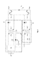
FIG. 1 is a diagram of a generalized embodiment. As shown in FIG. 1, an isolated power factor correction (PFC) circuit 10 outputs voltage Vo1 and an isolated ripple cancellation converter 20 outputs voltage Vo3. The output voltages Vo1 and Vo3 are connected in series with the load 50, which may be an LED. Output storage capacitors 42, 44 are shown for Vo1 and Vo3, respectively. Both output voltages contain low frequency ripple, however, the ripples are substantially out of phase with each other, such that they cancel each other. Two key tasks need to be done in order to achieve the ripple voltage cancellation and LED current regulation. First, the low frequency ripple of PFC output Vo1 and the output voltage Vo3 of the ripple cancellation converter need to be sensed, and this information used to shape the ripple cancellation converter output Vo3. Second, the LED current must be sensed and compared to a reference current to achieve current regulation. These two tasks are achieved at the primary side using a controller 30. It will be appreciated that such an embodiment may be implemented using only one integrated circuit (i.e., a primary side controller IC), as, for example, an application-specific integrated circuit
As illustrated in FIG. 1, the primary side controller 30 includes a first voltage sensor 31 and a second voltage sensor 33, that sense the PFC output and the RCC output, respectively, at the primary side. A level shifter 32 and a voltage controller 34 are also included in controller 30 so that the voltage control loop for the RCC output Vo3 is implemented at the primary side and Vo3 can be shaped as desired to match the ripple in Vo1. The primary side controller 30 also includes components such as a PFC controller 36 and a load (LED) current sensor 62. The current sensor output is compared with a current reference 38 in the PFC controller 36 to achieve load current regulation.
Detailed Operating Principle
Key features of an exemplary embodiment, based on a flyback topology, including power structure, PFC and ripple cancellation converter voltage sensing, LED current sensing, and control circuit will now be described in detail. However, it will be appreciated that the invention is not limited thereto, as the PFC and ripple cancellation converter may be implemented with other isolated power topologies, such as, for example, isolated boost, where the sensing of secondary side output voltage and LED current may need to vary accordingly.
Power Structure
As an example, FIG. 2 shows the power stage 10 constructed using flyback topology for the PFC and the ripple cancellation converter 20.
The LED voltage, Vout, is produced by connecting the flyback PFC output Vo1 and the ripple cancellation converter output Vo3 in series. The input DC voltage, Vo2, for the ripple cancellation converter is produced at the primary side by the flyback PFC.
The flyback PFC output voltage Vo1 contains a significant low frequency ripple component. The voltage Vo1 can be described by equation (1):
V o1 =V o1 _ dc +V o1 _ rip(t)  (1)
In equation (1), Vo1_dc represents the DC component of Vol while Vo1_rip(t) represents its low frequency ripple component. The ripple cancellation converter output Vo3 also contains a significant low frequency ripple component and is described by equation (2):
V o3 =V o3 _ dc +V o3 _ rip(t)  (2)
The DC component Vo3_dc is needed to maintain Vo3 above zero. The purpose of connecting voltage Vo1 and Vo3 in series is to have their ripple component canceled. As such, their sum, Vout, is a DC value and is described by equation (3):
V out = V o 1 + V o 3 = ( V o 1 _ d c + V o 3 _ d c ) + [ V o 1 _ rip ( t ) + V o 3 _ rip ( t ) ] ( 3 )
As can be seen from equation (3), in order to achieve total low frequency ripple cancellation, the following equation must be satisfied:
V o1 _ rip(t)+V o3 _ rip(t)=0  (4)
Equation (4) requires that Vo1_rip(t) and Vo3_rip(t) are of equal value but with opposite sign. In this disclosure, Vo1_rip(t) is the master signal and Vo3_rip(t) is its dependent follower.
Primary Side Voltage Sensing
In order to shape the ripple cancellation converter output Vo3, both Vo1 and Vo3 need to be sensed at the primary side. FIG. 3A shows a generalized embodiment of primary side voltage sensing employing a sample and hold (S&H) technique. Such primary side voltage sensing may be used for the voltage sensors 31 and 33 (FIG. 1). An a more detailed embodiment is shown in FIG. 3B, wherein waveforms of the voltage on the secondary side winding Vsec, the voltage on the primary side sensing winding Vsns, and the gating signal Vgs are illustrated.
In this example, for a flyback topology based power converter, when Q2 is turned off, both diodes D1 and D2 conduct. Therefore, the voltage across the secondary side winding, Vsec, is equal to the output voltage Vo3 (D2 forward voltage drop has been ignored). The sensed voltage Vsns and the secondary side voltage Vsec have a proportional relationship. This relationship is determined by the transformer turns ratio and is described by equation (5):
V sns = N sns N se c · V Se c ( 5 )
In equation (5), Nsns and Nsec represent he turns of the primary side sensing winding and the secondary side winding, respectively. Therefore, the output voltage of the flyback converter can be sensed at primary side. Similarly, the flyback PFC output voltage can also be sensed at primary side in the same way. In order to produce a continuous sensed voltage at the primary side instead of a pulsating value, the sensed voltage may be sampled during the Q2 turn off period while D2 is still conducting as shown in FIG. 3B. For practical concerns, the voltage sampling should be timed to avoid excessive voltage ringing, as typically occurs right after Q2 turns off, as shown by the arrows labelled “sample” in the plot of Vsns in FIG. 3B.
However, for the flyback PFC, during the zero crossing of the input voltage and current, the voltage on the sensing winding is distorted, As a result, the output of the voltage sensing is also distorted. Therefore, a modified primary side voltage sensing circuit such as that shown in FIG. 3C may be used. This embodiment adds a diode Ds, a capacitor Cs, and a resistor Rs to the sensing circuit, to filter out the sensed distortion. The embodiment of FIG. 3C may be particularly useful for the flyback PFC voltage sensor 31.
Primary Side Current Sensing
The load current is also sensed at the primary side, An example of a suitable technique is shown in FIG. 4. The average current flow into the secondary side during a switching period may be described by equation (6):
I se c _ avg = n × I pri _ pi × T dis 2 × T cyc ( 6 )
In equation (6), n represents the turn ratio (Npri:Nsec) of the primary side and the secondary side windings. Ipri_pk is the peak switching current at the primary side, Tdis and Tcyc represent the secondary side current discharge time and the whole switching period respectively. Ipri_pk and Tdis can be sensed at primary side. Tcyc is a known parameter predetermined by design. Thus, the average secondary side current at the primary side can be determined.
Current Regulation Loop
As discussed above, the average LED current is determined at the primary side. FIG. 5 is a diagram of a load current regulation loop 60 according to one embodiment, Such an embodiment may be implemented in the primary side controller 30 (FIG. 1). The embodiment includes an average current sensor 62, PFC controller 36 that receives the calculated average current I_avg and compares it with the current reference Iref_38. The PFC. controller 36 adjusts the output voltage of the flyback PFC 66. Thus, the LED current 68 may be regulated automatically.
Output Ripple Shaping for Ripple Cancellation Converter
FIG. 6 is a simplified diagram showing shaping of the ripple cancellation converter output Vo3. Such an embodiment may be implemented in the primary side controller 30 (FIG. 1). The figure shows primary side sensing of the flyback PFC 10 output Vol and the ripple cancellation converter 20 output Vo3 at the primary side, across the isolation barrier (dashed line) provided by the transformer. The technique may include components such as a level shifter 32 and voltage regulator 34. With proper signal conditioning of Vsns1, the reference voltage Vref for the ripple cancellation converter is produced. The output voltage of the ripple cancellation converter Vo3 is then shaped to cancel low frequency ripple in Vo1.
Variable Output Power
In some applications it might be desirable to vary (e.g., control) the output power of the converter. For example, in LED lighting applications, dimming of the LED may be required. The term “dimming” means that the light output of the LED is adjustable or variable. Some applications may require that the LED light is adjustable from 100% to 1%. Dimming may be achieved according to several techniques. In one such technique the load current is adjustable. For example, this may be achieved by controlling (e.g., varying) the output reference signal I_ref. Other techniques may include controlling the output power between two different levels according to, e.g., a variable duty cycle.
Features
High efficiency
As shown in FIG. 1, the averaged voltage of Vo1 and Vo3 are 45V and 5V, respectfully, delivering 90% of the output power by the flyback PFC directly, while 10% of the output power is delivered by the ripple cancellation converter. The power delivered by the flyback PFC has only been converted once. The input voltage of the ripple cancellation converter is an additional output of the flyback PFC located at the primary side, so the power delivered by ripple cancellation converter has been processed twice, Since the majority of the power delivered to the load has only been converted once, the overall efficiency of the driver embodiments is very close to that of a conventional flyback LED driver. Equation (7) describes the efficiency:
η new = 1 0.9 η PFC + 0.1 η PFC × η RCC ( 7 )
In equation (7), ηnew, ηPFC, ηRCC represent the overall efficiency of the driver, the efficiency of the flyback PFC, and the efficiency of the ripple cancellation converter, respectively. From equation 7 it can be seen that if 87% efficiency is achieved by the ripple cancellation converter, the overall efficiency can achieve 0.985ηPFC, which is very close to the efficiency of a comparable conventional flyback LED driver.
Low Component Cost
As discussed above, since the control circuit is located at the primary side, it can be implemented on a single IC, Therefore, only one controller is needed at the primary side for an isolated driver with ripple cancellation, which represents a substantial reduction in complexity and cost relative to prior designs.
EXAMPLES
Embodiments further described by way of the following non-limiting examples.
Example 1 LED Driver
FIG. 7 shows a block diagram of an embodiment of a primary side controlled LED driver with ripple cancellation. Vo1 and Vo3 are sensed at the primary side by sns1 winding of transformer T1 and sns3 winding of transformer T2, respectively. The LED current is sensed at the primary side via the current in transformer T2. The embodiment includes two control loops. One loop regulates the LED current and includes primary side current sensor 62 to generate I_avg, a PFC controller 36 that compares I_avg and I_ref, and generates a gating signal for primary side switch Q1 of the power circuit. The second loop controls the ripple cancellation converter output Vo3, and includes a first voltage sensor 31, a second voltage sensor 33, a level shifter 32, and RCC controller 34. The RCC controller 34 compares Vsns1 and Vsn3 and generates a gating signal for the switch Q2 of the ripple cancellation converter. The primary side controller 30 is highlighted by the dashed box. From FIG. 7 it can be seen that no secondary side control circuit and no isolation device (e.g., opto-coupler) are needed. An integrated primary side controller may be designed based on this circuit arrangement. As a result, the component cost and design complexity are reduced substantially.
Example 2 Experimental Results
A 35 W (50 V/0.7 A) experimental LED driver was built, based on the embodiment of FIG. 7, to verify the performance of the driver. The following components were used:
Flyback PFC Section
Transformer turns ratio Npri:Nsec 38:15
Primary side winding inductance (Lpri) 470 μH
MOSFET Q1 STF11NM80
PFC controller FA5601N
Output capacitor Co1 470 μF, 63 V
S & H HA5351IBZ
OpAmp TLV274
Ripple Cancellation Converter Section
Transformer turn ratio Npri:Nsec  1:1
Primary side winding inductance  19 μH
MOSFET Q2 ZXMN4A06GTA
RCC input capacitor C aux 160 μF, 16 V
RCC output capacitor C o2 20 μF, 16 V
RCC controller FAN6961
S & H HA5351IBZ
LED Load Section
LED load (23 LEDs connected in series) LR W5AM-HZJZ-1-Z
In order to conduct an objective evaluation, the performance of a conventional flyback LED driver and a two-stage (flyback PFC.+Buck DC-DC) LED driver were included for comparison. The plot of FIG. 8 compares the efficiency of the three designs. The ITC circuits in three designs were identical.
As shown in FIG. 8, the efficiency of the embodiment at 110 VAC input is 3% higher than the two-stage driver. At 220 VAC input, the embodiment achieves 2% higher efficiency than the two-stage driver. Since only 10% of the output power is handled by the ripple cancellation converter in the embodiment, the overall efficiency is very close to the conventional flyback driver and much higher than the two-stage LED driver.
FIGS. 9A and 9B show the low frequency ripple current of the experimental embodiment and the conventional flyback LED driver. Both drivers included a 470 μF output storage capacitor. The ripple cancellation converter embodiment produced a near-DC LED current, with a low frequency ripple of only 20 mA pk-pk. In contrast, the low frequency ripple current for the conventional flyback LED driver was 200 mA pk-pk.
The total harmonic distortion (THD) and power factor performance of the experimental embodiment and the conventional flyback driver are compared in FIGS. 10 and 11, respectively. The plots show that the THD and power factor of the experimental embodiment were very close to the conventional flyback LED driver.
FIG. 12 shows the ripple voltage sensing result of the flyback FTC output Vol and the ripple cancellation converter output Vo3 for the experimental embodiment. The plot confirms that high fidelity low frequency ripple information has been retrieved at the primary side. The primary side current sensing waveform is shown in FIG. 13A. In FIG. 13B the time scale has been expanded to show the waveforms.
Equivalents
Those skilled in the art will recognize or be able to ascertain variants of the embodiments described herein. Such variants are within the scope of the invention and are covered by the appended claims.

Claims (17)

The invention claimed is:
1. A circuit for use with a power supply including a primary input side and a secondary output side, wherein the primary input side comprises at least one first switch and the power supply provides a main output including a main DC voltage with a first AC voltage ripple or a main DC current with a first AC current ripple, the circuit comprising:
a primary side controlled isolated ripple cancellation converter comprising at least one second switch, wherein the primary side controlled isolated ripple cancellation converter:
(i) senses the first AC voltage ripple from the primary side; and
uses the sensed AC voltage ripple to provide a second AC voltage ripple;
wherein the second AC voltage ripple is connected in series with the main output, such that the first AC voltage ripple is substantially cancelled; or
(ii) senses the first AC current ripple from the primary side; and
uses the sensed AC current ripple to provide a second AC current ripple;
wherein the second AC current ripple is connected in parallel with the main output, such that the first AC current ripple is substantially cancelled;
wherein substantially ripple-free DC output power is provided to a load.
2. The power supply of claim 1, comprising:
a power circuit comprising the at least one first switch that outputs the main DC voltage with the first AC voltage ripple or the main DC current with the first AC current ripple; and
the primary side controlled isolated ripple cancellation converter.
3. The circuit of claim 1, wherein the ripple cancellation converter provides an auxiliary output comprising:
(i) an auxiliary DC voltage with the second AC voltage ripple, wherein the second AC voltage ripple is substantially equal in magnitude and substantially opposite in phase to the first AC voltage ripple;
wherein the main output and the auxiliary output are combined such that:
a total DC voltage is provided;
the second AC voltage ripple substantially cancels the first AC voltage ripple, or the total DC voltage is substantially ripple-free; or
(ii) an auxiliary DC current with the second AC current ripple, wherein the second AC current ripple is substantially equal in magnitude and substantially opposite in phase to the first AC current ripple;
wherein the main output and the auxiliary output are combined such that:
a total DC current is provided;
the second AC current ripple substantially cancels the first AC current ripple, or the total DC current is substantially ripple-free.
4. The circuit of claim 1, wherein the ripple cancellation converter comprises a flyback converter or an isolated boost converter.
5. The circuit of claim 1, further comprising:
a first primary side sensor that senses the first AC voltage ripple and outputs a first sensor signal;
a second primary side sensor that senses the second AC voltage ripple and outputs a second sensor signal; and
a primary side ripple cancellation controller that uses the first and second sensor signals to control the ripple cancellation converter to shape the second AC voltage ripple.
6. The circuit of claim 1, further comprising a power factor correction circuit.
7. The circuit of claim 6, wherein operation of the power factor correction circuit is based on a feedback signal derived from a primary side load current sensor.
8. The circuit of claim 1, wherein the substantially ripple-free DC output power is variable.
9. The circuit of claim 1, wherein the power supply is an AC-DC power supply.
10. The circuit of claim 1, wherein the load comprises at least one LED.
11. A method for providing DC power from a DC power supply comprising a primary side having an AC input and at least one first switch, the DC power supply providing a main output power comprising a main DC voltage with a first AC voltage ripple or a main DC current with a first AC current ripple, the method comprising:
controlling an isolated ripple cancellation converter comprising at least one second switch from the primary side, wherein controlling comprises:
(i) sensing the first AC voltage ripple from the primary side; and
using the sensed AC voltage ripple to provide a second AC voltage ripple;
wherein the second AC voltage ripple is connected in series with the main output, such that the first AC voltage ripple is substantially cancelled; or
(ii) sensing the first AC current ripple from the primary side; and
using the sensed AC current ripple to provide a second AC current ripple;
wherein the second AC current ripple is connected in parallel with the main output, such that the first AC current ripple is substantially cancelled;
wherein substantially ripple-free DC output power is provided to a load.
12. The method of claim 11, farther comprising:
(i) controlling the isolated ripple cancellation converter to output an auxiliary DC voltage with the second AC voltage ripple, wherein the second AC voltage ripple is substantially equal in magnitude and substantially opposite in phase to the first AC voltage ripple; and
combining the main output and the auxiliary DC voltage such that:
a total DC voltage is provided;
the second AC voltage ripple substantially cancels the first AC voltage ripple, or the total DC voltage is substantially ripple-free;
or
(ii) controlling the isolated ripple cancellation converter to output an auxiliary DC current with the second AC current ripple, wherein the second AC current ripple is substantially equal in magnitude and substantially opposite in phase to the first AC current ripple; and
combining the main output and the auxiliary DC current such that:
a total DC current is provided;
the second AC current ripple substantially cancels the first AC current ripple, or the total DC current is substantially ripple-free.
13. The method of claim 11, further comprising:
using a first primary side sensor to sense the first AC voltage ripple and output a first sensor signal;
using a second primary side sensor to sense the second AC voltage ripple and output a second sensor signal; and
using a primary side ripple cancellation controller to shape the second AC voltage ripple based on the first and second sensor signals.
14. The method of claim 11, further comprising:
using a primary side current sensor to sense the load current and output a feedback signal; and
controlling operation of a power factor correction circuit based on the feedback signal.
15. The method of claim 11, further comprising providing variable substantially ripple-free DC output power.
16. The method of claim 11, comprising applying the method to an AC-DC power supply.
17. The method of claim 11, wherein the load comprises at least one LED.
US15/125,271 2014-03-14 2015-03-13 Primary side controlled LED driver with ripple cancellation Active US10015848B2 (en)

Priority Applications (1)

Application Number Priority Date Filing Date Title
US15/125,271 US10015848B2 (en) 2014-03-14 2015-03-13 Primary side controlled LED driver with ripple cancellation

Applications Claiming Priority (3)

Application Number Priority Date Filing Date Title
US201461953264P 2014-03-14 2014-03-14
US15/125,271 US10015848B2 (en) 2014-03-14 2015-03-13 Primary side controlled LED driver with ripple cancellation
PCT/CA2015/000172 WO2015135073A1 (en) 2014-03-14 2015-03-13 Primary side controlled led driver with ripple cancellation

Publications (2)

Publication Number Publication Date
US20170079095A1 US20170079095A1 (en) 2017-03-16
US10015848B2 true US10015848B2 (en) 2018-07-03

Family

ID=54070732

Family Applications (1)

Application Number Title Priority Date Filing Date
US15/125,271 Active US10015848B2 (en) 2014-03-14 2015-03-13 Primary side controlled LED driver with ripple cancellation

Country Status (4)

Country Link
US (1) US10015848B2 (en)
CN (1) CN106464126A (en)
CA (1) CA2942423C (en)
WO (1) WO2015135073A1 (en)

Cited By (2)

* Cited by examiner, † Cited by third party
Publication number Priority date Publication date Assignee Title
US12095381B2 (en) 2019-10-25 2024-09-17 The Research Foundation For The State University Of New York Three phase bidirectional AC-DC converter with bipolar voltage fed resonant stages
US12301103B2 (en) * 2020-06-01 2025-05-13 Shenzhen Vmax New Energy Co., Ltd. Charging power supply circuit and control method of same

Families Citing this family (13)

* Cited by examiner, † Cited by third party
Publication number Priority date Publication date Assignee Title
WO2018040013A1 (en) * 2016-08-31 2018-03-08 Astec International Limited Power supplies having feedforward control using pulse modulation and demodulation
CN107426880B (en) * 2017-09-07 2023-04-18 上海晶丰明源半导体股份有限公司 LED current ripple eliminating circuit, method and chip thereof, and LED equipment
CN107426881B (en) * 2017-09-07 2023-09-22 上海晶丰明源半导体股份有限公司 Integrator, LED current ripple cancellation circuit and method
GB2570452B (en) * 2018-01-24 2022-04-06 Tridonic Gmbh & Co Kg Ripple-suppressing operating device for at least one LED
US10855166B2 (en) 2019-03-11 2020-12-01 Infineon Technologies Ag Ripple shaping for switch-mode power supply using number of active phases
AU2021220109A1 (en) * 2020-02-14 2022-09-15 HyGro Technology B.V. AC to DC converter for electrolysis
NL2024916B1 (en) * 2020-02-14 2021-09-15 Hygro Tech Bv AC to DC converter for electrolysis
CN112770451B (en) * 2021-01-27 2024-06-07 茂硕电源科技股份有限公司 Isolated AC-DC constant current driver and LED lighting equipment
CN112737370B (en) * 2021-01-27 2024-06-18 茂硕电源科技股份有限公司 AC/DC converter
CN112737069B (en) * 2021-01-27 2025-06-10 茂硕电源科技股份有限公司 AC/DC charger
US12439490B2 (en) * 2021-05-28 2025-10-07 Signify Holding B.V. Driver for driving a load, such as a LED load
NL2030193B1 (en) * 2021-12-20 2023-06-28 Eldolab Holding Bv LED driver
CN114205955B (en) * 2021-12-31 2024-04-05 福州大学 Single-stage low-ripple LED driving circuit and fusion VLC modulation method

Citations (8)

* Cited by examiner, † Cited by third party
Publication number Priority date Publication date Assignee Title
US5668708A (en) 1996-03-13 1997-09-16 Spellman High Voltage Electronics Corp. DC power supply with reduced ripple
US20050231133A1 (en) * 2004-03-15 2005-10-20 Color Kinetics Incorporated LED power control methods and apparatus
US7315150B1 (en) 2006-03-30 2008-01-01 Integrated Circuit Design, Inc. Method of power conversion and apparatus which achieves high power factor correction using ripple current mode control
US20120119676A1 (en) * 2010-11-15 2012-05-17 Power Integrations, Inc. Flyback power converter with divided energy transfer element
US8300438B1 (en) * 2008-11-16 2012-10-30 Edward Herbert Power factor corrected 3-phase Ac-dc power converter using natural modulation
WO2013056356A1 (en) 2011-10-17 2013-04-25 Queen's University At Kingston Ripple cancellation converter with high power factor
US20130313991A1 (en) 2012-05-23 2013-11-28 Luxul Technology Incorporation Flicker-free linear led driver circuit with high power factor
US20140049990A1 (en) * 2012-08-14 2014-02-20 Rudolf Limpaecher Soft-switching high voltage power converter

Family Cites Families (5)

* Cited by examiner, † Cited by third party
Publication number Priority date Publication date Assignee Title
CN2840508Y (en) * 2005-06-29 2006-11-22 闫克平 High frequency high voltage DC power supply for electric dust-cleaner
CN101741264A (en) * 2009-11-22 2010-06-16 杨义根 Three-phase power supply way of single-phase electric utensil
CN103200727A (en) * 2012-01-06 2013-07-10 欧司朗股份有限公司 Light-emitting diode (LED) driving circuit and lighting device comprising same
JP5140203B2 (en) * 2012-06-27 2013-02-06 パナソニック株式会社 LED lighting device
CN103152931A (en) * 2013-02-25 2013-06-12 南京航空航天大学 LED (light emitting diode) driving power supply with high power factor and without electrolytic capacity

Patent Citations (9)

* Cited by examiner, † Cited by third party
Publication number Priority date Publication date Assignee Title
US5668708A (en) 1996-03-13 1997-09-16 Spellman High Voltage Electronics Corp. DC power supply with reduced ripple
US20050231133A1 (en) * 2004-03-15 2005-10-20 Color Kinetics Incorporated LED power control methods and apparatus
US7315150B1 (en) 2006-03-30 2008-01-01 Integrated Circuit Design, Inc. Method of power conversion and apparatus which achieves high power factor correction using ripple current mode control
US8300438B1 (en) * 2008-11-16 2012-10-30 Edward Herbert Power factor corrected 3-phase Ac-dc power converter using natural modulation
US20120119676A1 (en) * 2010-11-15 2012-05-17 Power Integrations, Inc. Flyback power converter with divided energy transfer element
WO2013056356A1 (en) 2011-10-17 2013-04-25 Queen's University At Kingston Ripple cancellation converter with high power factor
US9419510B2 (en) 2011-10-17 2016-08-16 Queen's University At Kingston Ripple cancellation converter with high power factor
US20130313991A1 (en) 2012-05-23 2013-11-28 Luxul Technology Incorporation Flicker-free linear led driver circuit with high power factor
US20140049990A1 (en) * 2012-08-14 2014-02-20 Rudolf Limpaecher Soft-switching high voltage power converter

Non-Patent Citations (4)

* Cited by examiner, † Cited by third party
Title
Fang, P., et al., "Zero Ripple Single Stage AC-DC LED Driver with Unity Power Factor", IEEE, pp. 3452-3458, (2013).
International Search Report for International Application No. PCT/CA2015/000172 filed on Mar. 13, 2015.
Written Opinion for International Application No. PCT/CA2015/000172 filed on Mar. 13, 2015.
Xie, X., et al., "A Novel Output Current Estimation and Regulation Circuit for Primary Side Controlled High Power Factor Single-Stage Flyback LED Driver", IEEE Transactions on Power Electronics, vol. 27, No. 11, pp. 4602-4612, (2012).

Cited By (2)

* Cited by examiner, † Cited by third party
Publication number Priority date Publication date Assignee Title
US12095381B2 (en) 2019-10-25 2024-09-17 The Research Foundation For The State University Of New York Three phase bidirectional AC-DC converter with bipolar voltage fed resonant stages
US12301103B2 (en) * 2020-06-01 2025-05-13 Shenzhen Vmax New Energy Co., Ltd. Charging power supply circuit and control method of same

Also Published As

Publication number Publication date
US20170079095A1 (en) 2017-03-16
CA2942423C (en) 2020-11-24
CN106464126A (en) 2017-02-22
WO2015135073A1 (en) 2015-09-17
CA2942423A1 (en) 2015-09-17

Similar Documents

Publication Publication Date Title
US10015848B2 (en) Primary side controlled LED driver with ripple cancellation
US10015849B2 (en) Ripple cancellation converter with high power factor
US9525336B2 (en) Harmonic control method and circuit for flyback switching power supply
US9917524B2 (en) Energy channelling single stage power converter
US9318960B2 (en) High efficiency and low loss AC-DC power supply circuit and control method
KR101241470B1 (en) Apparatus for controlling current
US10256712B2 (en) Current ripple sensing controller for a single-stage LED driver
US10834793B2 (en) Power supply circuit and LED driving circuit
US20170279367A1 (en) High-Power Single-Stage LED Driver with Bipolar Ripple Cancellation
US20160150608A1 (en) Primary control led driver with additional power output and control method thereof
US20190149051A1 (en) A bifred converter and a method of driving an output load
US20150303813A1 (en) Ac-to-dc power converting device
JP2017070192A (en) Switching power supply device and LED lighting circuit
US20070138870A1 (en) Multi-output switching power supply
CN105958825B (en) A kind of primary current control driving circuit
US11622429B1 (en) QR-operated switching converter current driver
US20140132182A1 (en) Feedback circuit for non-isolated power converter
US11729883B1 (en) LED driver with auxiliary output and low standby power
JP2018137129A (en) LED lighting device and LED lighting device
US9318959B2 (en) Low total harmonic distortion and high power factor correction power converters
KR101219810B1 (en) Apparatus for controlling current
US7924584B1 (en) Power supply switching circuit for a halogen lamp
JP2016201169A (en) Led power supply device and led illumination device

Legal Events

Date Code Title Description
AS Assignment

Owner name: QUEEN'S UNIVERSITY AT KINGSTON, CANADA

Free format text: ASSIGNMENT OF ASSIGNORS INTEREST;ASSIGNORS:FANG, PENG;LIU, YAN-FEI;REEL/FRAME:040213/0681

Effective date: 20150917

STCF Information on status: patent grant

Free format text: PATENTED CASE

CC Certificate of correction
MAFP Maintenance fee payment

Free format text: PAYMENT OF MAINTENANCE FEE, 4TH YR, SMALL ENTITY (ORIGINAL EVENT CODE: M2551); ENTITY STATUS OF PATENT OWNER: SMALL ENTITY

Year of fee payment: 4