US10014829B2 - Non-inverting amplifier circuits - Google Patents
Non-inverting amplifier circuits Download PDFInfo
- Publication number
- US10014829B2 US10014829B2 US15/385,239 US201615385239A US10014829B2 US 10014829 B2 US10014829 B2 US 10014829B2 US 201615385239 A US201615385239 A US 201615385239A US 10014829 B2 US10014829 B2 US 10014829B2
- Authority
- US
- United States
- Prior art keywords
- transistor
- feedback
- input
- load
- electrically coupled
- Prior art date
- Legal status (The legal status is an assumption and is not a legal conclusion. Google has not performed a legal analysis and makes no representation as to the accuracy of the status listed.)
- Active
Links
Images


Classifications
-
- H—ELECTRICITY
- H03—ELECTRONIC CIRCUITRY
- H03F—AMPLIFIERS
- H03F1/00—Details of amplifiers with only discharge tubes, only semiconductor devices or only unspecified devices as amplifying elements
- H03F1/30—Modifications of amplifiers to reduce influence of variations of temperature or supply voltage or other physical parameters
- H03F1/306—Modifications of amplifiers to reduce influence of variations of temperature or supply voltage or other physical parameters in junction-FET amplifiers
-
- H—ELECTRICITY
- H03—ELECTRONIC CIRCUITRY
- H03F—AMPLIFIERS
- H03F1/00—Details of amplifiers with only discharge tubes, only semiconductor devices or only unspecified devices as amplifying elements
- H03F1/08—Modifications of amplifiers to reduce detrimental influences of internal impedances of amplifying elements
- H03F1/22—Modifications of amplifiers to reduce detrimental influences of internal impedances of amplifying elements by use of cascode coupling, i.e. earthed cathode or emitter stage followed by earthed grid or base stage respectively
- H03F1/223—Modifications of amplifiers to reduce detrimental influences of internal impedances of amplifying elements by use of cascode coupling, i.e. earthed cathode or emitter stage followed by earthed grid or base stage respectively with MOSFET's
-
- H—ELECTRICITY
- H03—ELECTRONIC CIRCUITRY
- H03F—AMPLIFIERS
- H03F1/00—Details of amplifiers with only discharge tubes, only semiconductor devices or only unspecified devices as amplifying elements
- H03F1/34—Negative-feedback-circuit arrangements with or without positive feedback
-
- H—ELECTRICITY
- H03—ELECTRONIC CIRCUITRY
- H03F—AMPLIFIERS
- H03F1/00—Details of amplifiers with only discharge tubes, only semiconductor devices or only unspecified devices as amplifying elements
- H03F1/34—Negative-feedback-circuit arrangements with or without positive feedback
- H03F1/342—Negative-feedback-circuit arrangements with or without positive feedback in field-effect transistor amplifiers
-
- H—ELECTRICITY
- H03—ELECTRONIC CIRCUITRY
- H03F—AMPLIFIERS
- H03F3/00—Amplifiers with only discharge tubes or only semiconductor devices as amplifying elements
- H03F3/45—Differential amplifiers
- H03F3/45071—Differential amplifiers with semiconductor devices only
- H03F3/45076—Differential amplifiers with semiconductor devices only characterised by the way of implementation of the active amplifying circuit in the differential amplifier
- H03F3/45179—Differential amplifiers with semiconductor devices only characterised by the way of implementation of the active amplifying circuit in the differential amplifier using MOSFET transistors as the active amplifying circuit
- H03F3/45183—Long tailed pairs
-
- H—ELECTRICITY
- H03—ELECTRONIC CIRCUITRY
- H03F—AMPLIFIERS
- H03F3/00—Amplifiers with only discharge tubes or only semiconductor devices as amplifying elements
- H03F3/45—Differential amplifiers
- H03F3/45071—Differential amplifiers with semiconductor devices only
- H03F3/45076—Differential amplifiers with semiconductor devices only characterised by the way of implementation of the active amplifying circuit in the differential amplifier
- H03F3/45376—Differential amplifiers with semiconductor devices only characterised by the way of implementation of the active amplifying circuit in the differential amplifier using junction FET transistors as the active amplifying circuit
- H03F3/45381—Long tailed pairs
- H03F3/4539—Folded cascode stages
-
- H—ELECTRICITY
- H03—ELECTRONIC CIRCUITRY
- H03F—AMPLIFIERS
- H03F2200/00—Indexing scheme relating to amplifiers
- H03F2200/372—Noise reduction and elimination in amplifier
-
- H—ELECTRICITY
- H03—ELECTRONIC CIRCUITRY
- H03F—AMPLIFIERS
- H03F2203/00—Indexing scheme relating to amplifiers with only discharge tubes or only semiconductor devices as amplifying elements covered by H03F3/00
- H03F2203/45—Indexing scheme relating to differential amplifiers
- H03F2203/45701—Indexing scheme relating to differential amplifiers the LC comprising one resistor
-
- H—ELECTRICITY
- H03—ELECTRONIC CIRCUITRY
- H03F—AMPLIFIERS
- H03F3/00—Amplifiers with only discharge tubes or only semiconductor devices as amplifying elements
- H03F3/45—Differential amplifiers
-
- H—ELECTRICITY
- H03—ELECTRONIC CIRCUITRY
- H03F—AMPLIFIERS
- H03F3/00—Amplifiers with only discharge tubes or only semiconductor devices as amplifying elements
- H03F3/45—Differential amplifiers
- H03F3/45071—Differential amplifiers with semiconductor devices only
Definitions
- Amplifier circuits are widely used in analog signal processing circuits.
- Amplifiers are commonly constructed with MOS transistors or bipolar transistors.
- MOS transistors the gate, the source, and the drain function as the control, reference, and output terminals, respectively.
- bipolar transistors the base, the emitter, and the collector function as the control, reference, and output terminals, respectively.
- CS common-source
- CG common-gate
- SF source-follower
- the corresponding amplifier types in bipolar technologies are the common-emitter (CE) amplifier, the common-base (CB) amplifier, and emitter follower (EF).
- the CS and CE amplifiers are most widely used due to their high voltage gain and high input impedance.
- the CG and CB amplifiers have better frequency response due to the lack of the Miller effect, but the low input impedance makes them difficult to drive.
- the CS, CE, CG, and CB amplifiers have large output resistance on the order of the load resistance, which makes it difficult for them to drive resistive loads.
- the SF and EF are unable to provide voltage gain, and are primarily employed as buffers.
- non-inverting amplifiers are required.
- CG and CB amplifiers are non-inverting, their low input impedance typically requires an additional buffer stage such as an SF or EF, thus increasing the power consumption, noise, and area.
- Non-inverting amplifiers with high input impedance are desirable in variety of applications, and power consumption, area, and noise preferably are minimized for longer battery life, portability, and performance. In addition, low output resistance and high power-supply rejection are desired in these amplifiers.
- various inventive embodiments disclosed herein generally relate to amplifier circuits that provide non-inverting amplification while providing high input impedance and low output impedance simultaneously.
- One embodiment is directed to an amplifier circuit comprising: an input transistor; a load transistor having a control terminal and a reference terminal; and a feedback transistor.
- the input transistor receives an input signal, the input transistor is electrically coupled to the load transistor and the feedback transistor, the control terminal of the load transistor is electrically coupled to a bias voltage, the feedback transistor is electrically coupled to the load transistor providing negative feedback, and the reference terminal of the load transistor serves as an output of the amplifier circuit.
- Another embodiment is directed to an amplifier circuit comprising: an input transistor; a load transistor having a control terminal and a reference terminal; a feedback transistor; and a current source.
- the input transistor receives an input signal
- the input transistor is electrically coupled to the load transistor and the feedback transistor
- the control terminal of the load transistor is electrically coupled to a bias voltage
- the feedback transistor is electrically coupled to the load transistor providing negative feedback
- the reference terminal of the load transistor serves as an output of the amplifier circuit.
- the current source is electrically coupled to the input transistor so as to increase the current through the input transistor.
- Another embodiment is directed to an amplifier circuit comprising: an input transistor; a load transistor having a control terminal and a reference terminal; a feedback transistor; and a level shifting circuit.
- the input transistor receives an input signal
- the input transistor is electrically coupled to the load transistor and the feedback transistor
- the control terminal of the load transistor is electrically coupled to a bias voltage
- the feedback transistor is electrically coupled to the load transistor providing negative feedback
- the reference terminal of the load transistor serves as an output of the amplifier circuit.
- the level shifting circuit electrically coupled to the load transistor and the feedback transistor, may be a capacitor charged to a predetermined voltage, a level shifting transistor and a current source, or resistor and a current source.
- the amplifier circuit comprises: a first input transistor; a second input transistor; at least one load transistor having a control terminal and a reference terminal; and at least one feedback transistor.
- the first and the second input transistors receive an input signal, the first input transistor is electrically coupled to the at least one load transistor and the at least one feedback transistor, the control terminal of the at least one load transistor is electrically coupled to a bias voltage, the at least one feedback transistor is electrically coupled to the at least one load transistor providing negative feedback.
- the reference terminal of the at least one load transistor serves as an output of the amplifier circuit.
- the amplifier circuit comprises: a first input transistor; a second input transistor; at least one load transistor having a control terminal and a reference terminal; at least one feedback transistor; and at least one positive feedback transistor.
- the first and the second input transistors receive an input signal, the first input transistor is electrically coupled to the at least one load transistor and the at least one feedback transistor, the control terminal of the at least one load transistor is electrically coupled to a bias voltage, the at least one feedback transistor is electrically coupled to the at least one load transistor providing negative feedback.
- the at least one positive feedback transistor is electrically coupled to the at least one load transistor to provide positive feedback.
- the reference terminal of the at least one load transistor serves as an output of the amplifier circuit.
- FIG. 1 provides an illustration of a prior art common-source amplifier.
- FIG. 2 (prior art) provides an illustration of a prior art common-gate amplifier.
- FIG. 3 (prior art) provides an illustration of a prior art source-coupled amplifier.
- FIG. 4A illustrates an example of an amplifier according to one embodiment of the present invention with an NMOS input transistor and PMOS load and feedback transistors.
- FIG. 4B illustrates an example of an amplifier according to another embodiment of the present invention with an NMOS input transistor, PMOS load and feedback transistors, and a current source.
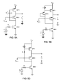
- FIG. 5A illustrates an example of an amplifier according to another embodiment of the present invention, which further includes a level shifting circuit implemented using a capacitor pre-changed to a predetermined voltage.
- FIG. 5B illustrates an example of an amplifier according to another embodiment of the present invention, which further includes a level shifting circuit implemented by a PMOS transistor and a current source.
- FIG. 5C illustrates an example of an amplifier according to another embodiment of the present invention, which further includes a level shifting circuit implemented by a resistor and a current source.
- FIG. 6 illustrates an example of an amplifier according to another embodiment of the present invention, with a PMOS input transistor and NMOS load and feedback transistors.
- FIG. 7 illustrates an example of an amplifier according to another embodiment of the present invention, with an NMOS input transistor and NMOS load and feedback transistors.
- FIG. 8 illustrates an example of an amplifier according to another embodiment of the present invention, with an NPN input transistor and PNP load and feedback transistors.
- FIG. 9A illustrates an example of an amplifier according to another embodiment of the present invention, with an NPN input transistor and PNP load and feedback transistors, further including a level shifting circuit implemented by a resistor and a current source.
- FIG. 9B illustrates an example of an amplifier according to another embodiment of the present invention, with an NPN input transistor and PNP load and feedback transistors, further including a level shifting circuit implemented by an NPN transistor and a current source.
- FIG. 9C illustrates an example of an amplifier according to another embodiment of the present invention, with an NPN input transistor and PNP load and feedback transistors, further including a level shifting circuit implemented by an VBE multiplier.
- FIG. 10 illustrates an example of a differential amplifier according to another embodiment of the present invention with an NMOS input transistors and PMOS load and feedback transistors.
- FIG. 11 illustrates an example of a differential amplifier according to another embodiment of the present invention with an NMOS input transistors, PMOS load and feedback transistors and positive feedback gain enhancement.
- FIG. 1 provides an illustration of a prior art CS amplifier circuit 20 with a load resistor R L and a source resistance R S .
- the incremental gain is shown to be: a v ⁇ g m1 R L (1) where g m1 is the transconductance of the input transistor M 1 .
- the incremental gain is negative, thus this amplifier provides inverting amplification.
- the input impedance at low frequencies is infinite, a desirable property for many applications.
- the output resistance of the amplifier 20 is approximately the same as the load resistor R L : R o ⁇ R L (2) Therefore, the CS amplifier's gain will be reduced if any resistive load is presented at the output. For example, if load resistance R 1 is attached between the output and the incremental ground, the corresponding incremental gain is reduced to a v ⁇ g m1 ( R L ⁇ R 1 ) (3) where (R L ⁇ R 1 ) is the equivalent resistance of R L in parallel with R 1 . Thus, unless R 1 is much larger than R L , the incremental gain is substantially reduced.
- the power supply rejection ratio (PSRR) of the amplifier in FIG. 1 is shown to be approximately same as the incremental gain because the power supply noise couples to the output without attenuation: PSRR ⁇ g m1 R L (4) This power supply rejection ratio is often lower than required.
- FIG. 2 provides an illustration of a prior art CG amplifier circuit 30 with a load resistor R L and a source resistance R S .
- the incremental gain is shown to be:
- the input impedance at low frequencies is approximately 1/g m1 , which is too low for applications where the source resistance R S is not very small.
- the incremental gain is reduced by a factor of 1+g m1 R S compared with that of the CS amplifier in FIG. 1 .
- the output resistance of the CG amplifier is approximately the same as the load resistor R L : R o ⁇ R L (6)
- the CG amplifier's gain will be reduced if any resistive load is presented at the output. For example, if load resistance R 1 is attached between the output and the incremental ground, the corresponding incremental gain is further reduced to
- the power supply rejection ratio of the CG amplifier in FIG. 2 is also shown to be approximately same as the incremental gain because the power supply noise couples to the output without attenuation as with the amplifier 20 in FIG. 1 :
- FIG. 3 provides an illustration of a prior art source-coupled amplifier circuit 40 with a load resistor R L and a source resistance R S .
- the SF comprising M 1 drives the CG amplifier comprising M 2 and R L .
- the incremental gain of this circuit is shown to be
- FIG. 4A shows an embodiment of an amplifier 50 according to the present invention.
- an NMOS transistor MN 1 constitutes the input transistor.
- a PMOS transistor MP 2 functions as a load transistor, and the PMOS transistor MP 1 functions as a feedback transistor.
- the bias voltage V BIAS is preferably referenced to the ground potential independent of the power supply, and adjusted in such way to bias all transistors in the saturation region.
- a negative feedback loop from the gate of MP 1 to the drain of MP 2 , and back to the gate of MP 1 adjusts the gate voltage of MP 1 so that the drain currents of MP 1 and MP 2 match the drain current of MN 1 .
- the source terminal of the load transistor MP 2 serves as an output of the amplifier 50 .
- g mn1 and g mp2 are the transconductance of the transistor MN 1 and MP 2 , respectively.
- the incremental gain is positive, thus this amplifier provides non-inverting amplification.
- the transconductance g mp2 is set to be:
- the input resistance is infinite at low frequencies as desired.
- the output resistance is given by
- the output resistance of the amplifier 50 is reduced by a large factor, 1+g mp1 r op1 , making it much easier for it to drive resistive loads as well as capacitive loads.
- the PSRR of the amplifier 50 is shown to be approximately PSRR ⁇ g mn1 ( r on1 ⁇ r op2 ) (15) where r on1 and r op2 are the output resistance of the transistor MN 1 and MP 2 , respectively.
- r on1 ⁇ r op2 is much larger than the load resistor R L , such that the PSRR of the amplifier according the present invention is higher than that of the prior art amplifiers in FIG. 1 , FIG. 2 , and FIG. 3 .
- FIG. 4B illustrates another embodiment of the present invention where a current source I provide higher bias current in the NMOS transistor MN 1 , thereby increasing its transconductance g m1 .
- a current source I provide higher bias current in the NMOS transistor MN 1 , thereby increasing its transconductance g m1 .
- higher g m1 provides higher gain and PSRR.
- the output swing which is the range of the output voltage for which both MP 1 and MP 2 are in the saturation region is given by
- and V GSP2 are the threshold voltages of MP 1 and MP 2
- are desired. Therefore, it may be preferred to employ a device type that offers the high threshold voltage for MP 1 .
- the gate length of MP 1 may also be chosen to maximize its threshold voltage. Reverse back-gate biasing may be employed to further increase the threshold voltage of MP 1 .
- FIG. 5A shows a level shifting circuit implemented by a capacitor charged to a predetermined voltage V 1 .
- FIG. 5B shows a level shifting circuit implemented using a PMOS transistor MP 3 and a current source I 1 .
- the gate-to-source voltage of MP 3 determines the level shift amount.
- FIG. 5C shows a level shifting circuit implemented by a resistor R 1 and a current source I 2 , where the level shift amount is I 1 R 1 .
- the power consumption of the amplifier 50 in FIG. 4A is comparable to that of the CS amplifier in FIG. 1 .
- the input referred noise is comparable to the CS amplifier if the incremental gain is made to be the same. Therefore there is no power or noise penalty in the amplifier circuit of FIG. 4 , and the area penalty of the additional transistor is small.
- FIG. 6 shows another embodiment of the present invention. It is a “flipped” version of the amplifier 50 in FIG. 4A , having a PMOS input transistor MP 1 and an NMOS load transistor MN 2 , and an NMOS feedback transistor MN 1 . Except for the flipped topology, the properties of the amplifier 60 are similar to those of the amplifier 50 .
- FIG. 7 shows another embodiment of the present invention. It is a “folded” version of the amplifier 50 in FIG. 4A , having NMOS input transistor MN 1 and an NMOS load transistor MN 3 and NMOS feedback transistor MN 2 .
- the current source I 1 supplies the bias currents for all transistors MN 1 , MN 2 , and MN 3 .
- the amplifier 70 functions similarly to the amplifier 60 in FIG. 6 .
- FIG. 8 shows an embodiment of the present invention using bipolar transistors.
- An NPN transistor QN 1 constitutes the input transistor.
- a PNP transistor QP 1 functions as the feedback transistor, and a PNP transistor QP 2 functions as the load transistor.
- the resistor R 1 effectively increases gain.
- the bias voltage V BIAS is preferably referenced to the ground potential independent of the power supply, and adjusted in such way to bias all transistors in the forward active region.
- a negative feedback loop from the base of QP 1 to the collector of QP 2 , and back to the base of QP 1 adjusts the base voltage of QP 1 so that the collector currents of QP 1 and QP 2 match the collector current of QN 1 .
- g mn1 and g mp2 are the transconductance of the transistor QN 1 and QP 2 , respectively.
- the incremental gain is positive, thus this amplifier provides non-inverting amplification.
- the resistor R 1 and transconductance g mp2 is set to be:
- the input resistance is r ⁇ 1 at low frequencies as in a CE amplifier.
- the output resistance is given by
- the PSRR is shown to be approximately PSRR ⁇ g mn1 ( r on1 ⁇ r op2 ) (20) where r on1 and r op2 are the output resistance of the transistor QN 1 and QP 2 , respectively.
- r on1 ⁇ r op2 is much larger than the load resistor R L , such that the PSRR of the amplifier according the present invention is higher than that of CE or CB amplifiers.
- the power consumption is comparable to that of a CE amplifier. 1.
- the input referred noise is comparable to the CE amplifier if the incremental gain is made to be the same. Therefore, there is no power or noise penalty in the amplifier circuit of FIG. 8 , and the area penalty of the additional transistor is small.
- FIG. 9A shows a level shifting circuit implemented by a resistor R 2 and a current source I 1 , where the level shift amount is I 1 R 2 .
- FIG. 9B shows a level shifting circuit implemented using a PNP transistor QP 3 and a current source I 1 . The base-to-emitter voltage of QP 3 determines the level shift amount.
- FIG. 9C shows a level shifting circuit implemented by a V BE multiplier. The level shift amount is given by
- V 1 R 2 + R 3 R 2 ⁇ V BEn ⁇ ⁇ 2 ( 21 ) where V BEn2 is the base-to-emitter voltage of the transistor QN 2 .
- the current source I 1 may be omitted in the level shifting circuits shown in FIG. 9A , FIG. 9B , and FIG. 9C .
- FIG. 10 illustrates another embodiment of the present invention in a differential amplifier 85 .
- the NMOS transistors MN 1 and MN 2 form the input differential pair.
- the PMOS transistors MP 1 and MP 3 function as the feedback transistors, and MP 2 and MP 4 function as the load transistors.
- the bias voltage VBIAS is preferably referenced to the ground potential for higher PSRR.
- a negative feedback loop from the gate of MP 1 to the drain of MP 2 , and back to the gate of MP 1 adjusts the gate voltage of MP 1 so that the drain currents of MP 1 and MP 2 match the drain current of MN 1 .
- another negative feedback loop from the gate of MP 3 to the drain of MP 4 , and back to the gate of MP 3 adjusts the gate voltage of MP 3 so that the drain currents of MP 3 and MP 4 match the drain current of MN 4 .
- the outputs are obtained from the source terminals of the load transistors MP 2 and MP 4 .
- g mn1 and g mp2 are the transconductance of the transistor MN 1 and MP 2 , respectively
- g mn2 and g mp4 are the transconductance of the transistor MN 2 and MP 4 , respectively.
- the incremental gain is positive, thus this amplifier provides non-inverting amplification.
- the input resistance is infinite at low frequencies as desired.
- the amplifier 85 provides superior PSRR compared with prior art differential amplifiers for the same differential gain.
- FIG. 11 illustrates another embodiment of the present invention with gain enhancement by positive feedback in an amplifier 90 .
- the PMOS transistors MP 5 and MP 7 as well as cascode transistors MP 6 and MP 8 are added.
- the PMOS transistors MP 5 and MP 7 provide positive feedback to increase the incremental gain.
- the cascode transistors MP 6 and MP 8 keep the drain voltages of MP 5 and MP 7 substantially equal to those of MP 1 and MP 3 , respectively, for better matching of operating voltages between MP 1 /MP 3 and MP 5 /MP 7 .
- the source terminals of the load transistor MP 2 and MP 4 serve as an output of the amplifier 90 .
- the incremental gain of the amplifier 90 is given by
- the bias voltage VBIAS 1 is adjusted such that the drain currents of MP 5 /MP 7 are made equal to those of MP 1 /MP 3
- the incremental gain becomes very large.
- the technology described herein may be embodied as a method, of which at least one example has been provided.
- the acts performed as part of the method may be ordered in any suitable way. Accordingly, embodiments may be constructed in which acts are performed in an order different than illustrated, which may include performing some acts simultaneously, even though shown as sequential acts in illustrative embodiments.
- a reference to “A and/or B”, when used in conjunction with open-ended language such as “comprising” can refer, in one embodiment, to A only (optionally including elements other than B); in another embodiment, to B only (optionally including elements other than A); in yet another embodiment, to both A and B (optionally including other elements); etc.
- the phrase “at least one,” in reference to a list of one or more elements, should be understood to mean at least one element selected from any one or more of the elements in the list of elements, but not necessarily including at least one of each and every element specifically listed within the list of elements and not excluding any combinations of elements in the list of elements.
- This definition also allows that elements may optionally be present other than the elements specifically identified within the list of elements to which the phrase “at least one” refers, whether related or unrelated to those elements specifically identified.
- “at least one of A and B” can refer, in one embodiment, to at least one, optionally including more than one, A, with no B present (and optionally including elements other than B); in another embodiment, to at least one, optionally including more than one, B, with no A present (and optionally including elements other than A); in yet another embodiment, to at least one, optionally including more than one, A, and at least one, optionally including more than one, B (and optionally including other elements); etc.
Landscapes
- Engineering & Computer Science (AREA)
- Power Engineering (AREA)
- Amplifiers (AREA)
Abstract
Description
a v ≈−g m1 R L (1)
where gm1 is the transconductance of the input transistor M1. As indicated by the minus sign, the incremental gain is negative, thus this amplifier provides inverting amplification. The input impedance at low frequencies is infinite, a desirable property for many applications.
R o ≈R L (2)
Therefore, the CS amplifier's gain will be reduced if any resistive load is presented at the output. For example, if load resistance R1 is attached between the output and the incremental ground, the corresponding incremental gain is reduced to
a v ≈−g m1(R L ∥R 1) (3)
where (RL∥R1) is the equivalent resistance of RL in parallel with R1. Thus, unless R1 is much larger than RL, the incremental gain is substantially reduced.
PSRR≈g m1 R L (4)
This power supply rejection ratio is often lower than required.
where gm1 is the transconductance of the transistor M1. The incremental gain is positive, thus this amplifier provides non-inverting amplification.
R o ≈R L (6)
Thus, unless R1 is much larger than RL, the incremental gain is substantially reduced.
Due to the lower incremental gain of the CG amplifier compared with that of a CS amplifier, the PSRR of the CG amplifier is often too low to be acceptable.
where gm1 and gm2 are the transconductance of the transistor M1 and M2, respectively. The incremental gain is positive, thus this amplifier provides non-inverting amplification. The input resistance is infinite at low frequencies as in the CS amplifier of
compared with that of the CS amplifier.
where gmn1 and gmp2 are the transconductance of the transistor MN1 and MP2, respectively. The incremental gain is positive, thus this amplifier provides non-inverting amplification. If same voltage gain is desired as that of the CS amplifier, the transconductance gmp2 is set to be:
such that
a v ≈g mn1 R L (12)
where gmp1 and rop1 are the transconductance and output resistance of the transistor MP1, respectively. If gmp2 is set according to Equation (11), the output resistance is
PSRR≈g mn1(r on1 ∥r op2) (15)
where ron1 and rop2 are the output resistance of the transistor MN1 and MP2, respectively. Typically, ron1∥rop2 is much larger than the load resistor RL, such that the PSRR of the amplifier according the present invention is higher than that of the prior art amplifiers in
where gmn1 and gmp2 are the transconductance of the transistor QN1 and QP2, respectively. The incremental gain is positive, thus this amplifier provides non-inverting amplification. If same voltage gain is desired as that of a CE amplifier, the resistor R1 and transconductance gmp2 is set to be:
such that
a v ≈g mn1 R L
where βop1 is the current gain of QP1, and gmp1 and rop1 are the transconductance and output resistance of the transistor QP1, respectively. If R1 and gmp2 are set according to Equation (17), the output resistance is
The output resistance of the
PSRR≈g mn1(r on1 ∥r op2) (20)
where ron1 and rop2 are the output resistance of the transistor QN1 and QP2, respectively. Typically, ron1∥rop2 is much larger than the load resistor RL, such that the PSRR of the amplifier according the present invention is higher than that of CE or CB amplifiers.
where VBEn2 is the base-to-emitter voltage of the transistor QN2.
where the differential input and output voltages vid and vod are defined as
v id =v 1 −v 2
v od =v o1 −v o2
Also, gmn1 and gmp2 are the transconductance of the transistor MN1 and MP2, respectively, and gmn2 and gmp4 are the transconductance of the transistor MN2 and MP4, respectively. The incremental gain is positive, thus this amplifier provides non-inverting amplification. The input resistance is infinite at low frequencies as desired.
As evident in Equation (23), if the sizes of MP5/MP7 are made equal to those of MP1/MP3, and the bias voltage VBIAS1 is adjusted such that the drain currents of MP5/MP7 are made equal to those of MP1/MP3, gmp1=gmp3=gmp5=gmp7, and the incremental gain becomes very large.
Claims (15)
Priority Applications (1)
| Application Number | Priority Date | Filing Date | Title |
|---|---|---|---|
| US15/385,239 US10014829B2 (en) | 2015-12-23 | 2016-12-20 | Non-inverting amplifier circuits |
Applications Claiming Priority (3)
| Application Number | Priority Date | Filing Date | Title |
|---|---|---|---|
| US201562387470P | 2015-12-23 | 2015-12-23 | |
| US201662298967P | 2016-02-23 | 2016-02-23 | |
| US15/385,239 US10014829B2 (en) | 2015-12-23 | 2016-12-20 | Non-inverting amplifier circuits |
Publications (2)
| Publication Number | Publication Date |
|---|---|
| US20170187333A1 US20170187333A1 (en) | 2017-06-29 |
| US10014829B2 true US10014829B2 (en) | 2018-07-03 |
Family
ID=59087430
Family Applications (1)
| Application Number | Title | Priority Date | Filing Date |
|---|---|---|---|
| US15/385,239 Active US10014829B2 (en) | 2015-12-23 | 2016-12-20 | Non-inverting amplifier circuits |
Country Status (2)
| Country | Link |
|---|---|
| US (1) | US10014829B2 (en) |
| CN (1) | CN106911310B (en) |
Citations (6)
| Publication number | Priority date | Publication date | Assignee | Title |
|---|---|---|---|---|
| US4264874A (en) * | 1978-01-25 | 1981-04-28 | Harris Corporation | Low voltage CMOS amplifier |
| US20020084855A1 (en) * | 2000-12-28 | 2002-07-04 | Kwon Ick Jin | Low power low noise amplifier |
| US6885250B1 (en) * | 2002-11-22 | 2005-04-26 | Advanced Micro Devices, Inc. | Cascode amplifier circuit for generating and maintaining a fast, stable and accurate bit line voltage |
| US6980050B2 (en) * | 2003-04-08 | 2005-12-27 | Via Technologies, Inc. | Differential amplifier and comparator using the same |
| US7576610B2 (en) * | 2006-05-31 | 2009-08-18 | Stmicroelectronics S.R.L. | Operational amplifier of class AB |
| US20140043100A1 (en) * | 2012-08-10 | 2014-02-13 | Lsi Corporation | Operational amplifier with improved frequency compensation |
Family Cites Families (5)
| Publication number | Priority date | Publication date | Assignee | Title |
|---|---|---|---|---|
| CN1138337C (en) * | 1999-10-08 | 2004-02-11 | 李希强 | Common collector-common base and common collector-common base-common collector transistor amplifier circuit |
| US6621348B2 (en) * | 2001-10-25 | 2003-09-16 | Motorola, Inc. | Variable gain amplifier with autobiasing supply regulation |
| US6856197B1 (en) * | 2003-07-28 | 2005-02-15 | Electronic Topologies, Inc. | Symmetrical current amplifier |
| KR101163457B1 (en) * | 2006-02-24 | 2012-07-18 | 삼성전자주식회사 | Low Voltage Regulated Cascade Circuits and CMOS Analog Circuits |
| US7633345B2 (en) * | 2007-12-26 | 2009-12-15 | Mediatek Inc. | Amplifier and the method thereof |
-
2016
- 2016-12-20 US US15/385,239 patent/US10014829B2/en active Active
- 2016-12-22 CN CN201611201119.0A patent/CN106911310B/en active Active
Patent Citations (7)
| Publication number | Priority date | Publication date | Assignee | Title |
|---|---|---|---|---|
| US4264874A (en) * | 1978-01-25 | 1981-04-28 | Harris Corporation | Low voltage CMOS amplifier |
| US20020084855A1 (en) * | 2000-12-28 | 2002-07-04 | Kwon Ick Jin | Low power low noise amplifier |
| US6885250B1 (en) * | 2002-11-22 | 2005-04-26 | Advanced Micro Devices, Inc. | Cascode amplifier circuit for generating and maintaining a fast, stable and accurate bit line voltage |
| US6980050B2 (en) * | 2003-04-08 | 2005-12-27 | Via Technologies, Inc. | Differential amplifier and comparator using the same |
| US7576610B2 (en) * | 2006-05-31 | 2009-08-18 | Stmicroelectronics S.R.L. | Operational amplifier of class AB |
| US20140043100A1 (en) * | 2012-08-10 | 2014-02-13 | Lsi Corporation | Operational amplifier with improved frequency compensation |
| US8766726B2 (en) * | 2012-08-10 | 2014-07-01 | Lsi Corporation | Operational amplifier with improved frequency compensation |
Also Published As
| Publication number | Publication date |
|---|---|
| CN106911310A (en) | 2017-06-30 |
| US20170187333A1 (en) | 2017-06-29 |
| CN106911310B (en) | 2020-09-29 |
Similar Documents
| Publication | Publication Date | Title |
|---|---|---|
| CN103907285B (en) | Differential amplifier | |
| US9874893B2 (en) | Self-biased multiple cascode current mirror circuit | |
| KR101485725B1 (en) | System | |
| US8410854B2 (en) | Semiconductor integrated circuit device | |
| Taherzadeh-Sani et al. | A 1-V process-insensitive current-scalable two-stage opamp with enhanced DC gain and settling behavior in 65-nm digital CMOS | |
| EP3335313B1 (en) | Multi-stage amplifier with cascode stage and dc bias regulator | |
| US8310308B1 (en) | Wide bandwidth class C amplifier with common-mode feedback | |
| Cellucci et al. | 0.6‐V CMOS cascode OTA with complementary gate‐driven gain‐boosting and forward body bias | |
| JP7005022B2 (en) | Amplifier | |
| US9571052B1 (en) | Transconductance (gm) boosting transistor arrangement | |
| US20160062385A1 (en) | Generating a current with inverse supply voltage proportionality | |
| Sansen | Analog design procedures for channel lengths down to 20 nm | |
| KR20180111577A (en) | Transconductance amplifier | |
| Nischal et al. | Study of a self biased high swing cascode current mirror based folded cascode operational amplifier | |
| US10014829B2 (en) | Non-inverting amplifier circuits | |
| CN111384940B (en) | High-linearity wide-swing CMOS voltage follower | |
| Malavolta et al. | A self-biased operational amplifier of constant gm for 1.5 V rail-to-rail operation in 130nm CMOS | |
| US9998080B2 (en) | Low voltage supply amplifier | |
| JP2007094800A (en) | Reference voltage generation circuit | |
| Singh et al. | Design and Analysis of DTMOS based Operational Transconductance Amplifier | |
| US7852157B2 (en) | Differential amplifier | |
| KR100961441B1 (en) | Bulk Driven OTI Circuit | |
| Veldandi et al. | A 1-V high-gain two-stage self-cascode operational transconductance amplifier | |
| CN101534101A (en) | differential amplifier | |
| US9374050B1 (en) | Level-shifting amplifier |
Legal Events
| Date | Code | Title | Description |
|---|---|---|---|
| AS | Assignment |
Owner name: OMNI DESIGN TECHNOLOGIES, INC., CALIFORNIA Free format text: ASSIGNMENT OF ASSIGNORS INTEREST;ASSIGNOR:LEE, HAE-SEUNG;REEL/FRAME:040776/0773 Effective date: 20161220 |
|
| STCF | Information on status: patent grant |
Free format text: PATENTED CASE |
|
| MAFP | Maintenance fee payment |
Free format text: PAYMENT OF MAINTENANCE FEE, 4TH YR, SMALL ENTITY (ORIGINAL EVENT CODE: M2551); ENTITY STATUS OF PATENT OWNER: SMALL ENTITY Year of fee payment: 4 |
|
| MAFP | Maintenance fee payment |
Free format text: PAYMENT OF MAINTENANCE FEE, 8TH YR, SMALL ENTITY (ORIGINAL EVENT CODE: M2552); ENTITY STATUS OF PATENT OWNER: SMALL ENTITY Year of fee payment: 8 |