TWI856552B - Memory device and compensation method of data retention thereof - Google Patents
Memory device and compensation method of data retention thereof Download PDFInfo
- Publication number
- TWI856552B TWI856552B TW112108611A TW112108611A TWI856552B TW I856552 B TWI856552 B TW I856552B TW 112108611 A TW112108611 A TW 112108611A TW 112108611 A TW112108611 A TW 112108611A TW I856552 B TWI856552 B TW I856552B
- Authority
- TW
- Taiwan
- Prior art keywords
- threshold voltage
- voltage
- memory cells
- charge loss
- memory cell
- Prior art date
Links
- 238000000034 method Methods 0.000 title claims abstract description 24
- 230000014759 maintenance of location Effects 0.000 title claims abstract description 14
- 238000012795 verification Methods 0.000 claims description 22
- 238000001514 detection method Methods 0.000 claims description 5
- 238000010586 diagram Methods 0.000 description 8
- 238000005192 partition Methods 0.000 description 8
- 238000004321 preservation Methods 0.000 description 6
- 238000013500 data storage Methods 0.000 description 2
- RJCRUVXAWQRZKQ-UHFFFAOYSA-N oxosilicon;silicon Chemical compound [Si].[Si]=O RJCRUVXAWQRZKQ-UHFFFAOYSA-N 0.000 description 2
- 239000000047 product Substances 0.000 description 2
- 229910052814 silicon oxide Inorganic materials 0.000 description 2
- 230000000153 supplemental effect Effects 0.000 description 2
- 230000007613 environmental effect Effects 0.000 description 1
- 230000007774 longterm Effects 0.000 description 1
- 239000013589 supplement Substances 0.000 description 1
- 230000001502 supplementing effect Effects 0.000 description 1
Images


Landscapes
- Read Only Memory (AREA)
Abstract
Description
本發明是有關於一種記憶體裝置及其補償方法,且特別是有關於一種透過補充程式化動作來補償資料保存度的記憶體裝置及其補償方法。The present invention relates to a memory device and a compensation method thereof, and in particular to a memory device and a compensation method thereof that compensates for data retention by supplementing programmed actions.
隨著電子科技的進步,電子產品成為人們生或中的重要工具。而為了提供可信賴且大量的資料訊息,在電子產品中設置高可靠度的記憶體裝置是一個必然的趨勢。With the advancement of electronic technology, electronic products have become an important tool in people's lives. In order to provide reliable and large amounts of data information, it is an inevitable trend to install high-reliability memory devices in electronic products.
在現今的技術領域中,快閃記憶體裝置成為電子裝置中,做為資料儲存媒介的一種主流。然而,快閃記憶胞在高度的讀取抹除循環(program and erase cycle, PE cycle)下,可能造成可靠度的下降。可靠度下降的快閃記憶胞,其具有的電荷保存能力的可下降,在長時間的儲存條件下,記憶胞中的電荷可能發生損失(charge loss)而造成資料保存度下降。In today's technology, flash memory devices have become a mainstream data storage medium in electronic devices. However, flash memory cells may have reduced reliability under high program and erase cycles (PE cycles). Flash memory cells with reduced reliability may have reduced charge retention capacity. Under long-term storage conditions, the charge in the memory cell may be lost (charge loss) and cause data retention to decrease.
本發明提供一種記憶體裝置及其資料保存度的補償方法,可有效維持已程式化記憶胞的儲存電荷。The present invention provides a memory device and a data retention compensation method thereof, which can effectively maintain the storage charge of programmed memory cells.
本發明的資料保存度的補償方法包括:針對記憶體裝置中的多個已程式化記憶胞的每一者進行讀取動作;透過讀取動作以判斷各程式化記憶胞是否發生電荷損失現象來設定各程式化記憶胞為電荷損失記憶胞;以及,針對電荷損失記憶胞執行補充程式化動作。The data retention compensation method of the present invention includes: performing a read operation on each of a plurality of programmed memory cells in a memory device; determining whether charge loss occurs in each programmed memory cell through the read operation to set each programmed memory cell as a charge loss memory cell; and performing a supplementary programming operation on the charge loss memory cell.
本發明的記憶體裝置包括記憶體區塊以及控制器。控制器耦接記憶體區塊。控制器用以:針對記憶體裝置中的多個已程式化記憶胞的每一者進行讀取動作;透過讀取動作以判斷各程式化記憶胞是否發生電荷損失現象來設定各程式化記憶胞為電荷損失記憶胞;以及,針對電荷損失記憶胞執行補充程式化動作。The memory device of the present invention includes a memory block and a controller. The controller is coupled to the memory block. The controller is used to: perform a read operation on each of a plurality of programmed memory cells in the memory device; determine whether charge loss occurs in each programmed memory cell through the read operation to set each programmed memory cell as a charge loss memory cell; and perform a supplementary programming operation on the charge loss memory cell.
基於上述,本發明的記憶體裝置透過針對記憶胞的電荷損失狀態進行檢測,並在檢測出記憶胞發生電荷損失現象時,針對電荷損失記憶胞執行補充程式化動作。如此一來,記憶胞的電荷損失現象可以得到補償,並維持資料的可靠度。Based on the above, the memory device of the present invention detects the charge loss state of the memory cell, and when the charge loss phenomenon of the memory cell is detected, the memory cell is supplemented with a programmed action. In this way, the charge loss phenomenon of the memory cell can be compensated and the reliability of the data can be maintained.
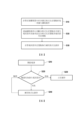
請參照圖1,圖1繪示本發明一實施例的資料保存度的補償方法的流程圖。在步驟S110中,可針對記憶體裝置中的多個已程式化記憶胞的每一者進行一讀取動作,並在步驟S120中,透過上述的讀取動作以判斷各個程式化記憶胞是否發生電荷損失現象。並根據各個程式化記憶胞是否發生電荷損失現象,來設定各個程式化記憶胞為電荷損失記憶胞。在細節上,本發明實施例中,可針對整個記憶體裝置中,所有的已程式化記憶胞進行是否發生電荷損失現象的檢測動作。上述的電荷損失現象的檢測動作,可針對各個已程式化記憶胞進行讀取動作來進行。透過讀取動作,可以檢測出各個已程式化記憶胞的臨界電壓的飄移狀態。在本發明實施例中,記憶體裝置內可先設置第一閾值電壓以及第二閾值電壓,其中第二閾值電壓大於第一閾值電壓,且第二閾值電壓可小於已程式化記憶胞在前次執行程式化動作中的程式化驗證電壓。記憶體裝置並可判斷受檢測的已程式化記憶胞的臨界電壓是否落於第一閾值電壓以及第二閾值電壓間。當受檢測的已程式化記憶胞的臨界電壓落於第一閾值電壓以及第二閾值電壓間,記憶體裝置可判定受檢測的已程式化記憶胞發生電荷損失現象,並可被設定為電荷損失記憶胞。當受檢測的已程式化記憶胞的臨界電壓並非落於第一閾值電壓以及第二閾值電壓間,記憶體裝置則不設定受檢測的已程式化記憶胞為電荷損失記憶胞。Please refer to FIG. 1, which shows a flow chart of a data retention compensation method of an embodiment of the present invention. In step S110, a read operation can be performed for each of the multiple programmed memory cells in the memory device, and in step S120, the above-mentioned read operation is used to determine whether each programmed memory cell has a charge loss phenomenon. And according to whether each programmed memory cell has a charge loss phenomenon, each programmed memory cell is set as a charge loss memory cell. In detail, in the embodiment of the present invention, a detection operation can be performed on all programmed memory cells in the entire memory device to determine whether a charge loss phenomenon has occurred. The above-mentioned charge loss phenomenon detection operation can be performed by performing a read operation on each programmed memory cell. Through the read operation, the drift state of the critical voltage of each programmed memory cell can be detected. In the embodiment of the present invention, a first threshold voltage and a second threshold voltage can be set in the memory device, wherein the second threshold voltage is greater than the first threshold voltage, and the second threshold voltage can be less than the programming verification voltage of the programmed memory cell in the previous execution of the programming operation. The memory device can also determine whether the critical voltage of the detected programmed memory cell falls between the first threshold voltage and the second threshold voltage. When the critical voltage of the detected programmed memory cell falls between the first threshold voltage and the second threshold voltage, the memory device can determine that the detected programmed memory cell has charge loss and can be set as a charge loss memory cell. When the critical voltage of the detected programmed memory cell does not fall between the first threshold voltage and the second threshold voltage, the memory device does not set the detected programmed memory cell as a charge loss memory cell.
在本發明其他實施例中,可基於記憶體裝置中的多個分區來執行電荷損失現象的檢測動作。其中,記憶體裝置中的每一分區可以為已抹除分區以及已程式化分區。記憶體裝置可針對已程式化分區中的已程式化記憶胞進行讀取動作以判定各個已程式化記憶胞是否為電荷損失記憶胞。記憶體裝置可不針對已抹除分區進行讀取動作。In other embodiments of the present invention, the charge loss phenomenon detection operation can be performed based on multiple partitions in the memory device. Each partition in the memory device can be an erased partition and a programmed partition. The memory device can perform a read operation on the programmed memory cells in the programmed partition to determine whether each programmed memory cell is a charge loss memory cell. The memory device may not perform a read operation on the erased partition.
接著,在步驟S130中,記憶體裝置可針對電荷損失記憶胞執行補充程式化動作,並透過補充程式化動作對電荷損失記憶胞進行電荷再填補(refill)動作,並完成記憶胞的資料保存度的補償動作。Next, in step S130, the memory device may perform a supplementary programming operation on the charge-loss memory cell, and perform a charge refill operation on the charge-loss memory cell through the supplementary programming operation, and complete the data retention compensation operation of the memory cell.
在本實施例中,在補充程式化動作,記憶體裝置可設定一程式化電壓,並提供具有程式化電壓的單一脈波對電荷損失記憶胞執行補充程式化動作。在本實施方式中,補充程式化動作可程式化電壓可大於補充程式化驗證動作的程式化驗證電壓。而上述的程式化驗證電壓可以根據上述的第二閾值來設定,例如使程式化驗證電壓等於上述的第二閾值。In this embodiment, in the supplementary programming action, the memory device can set a programming voltage and provide a single pulse with the programming voltage to perform the supplementary programming action on the charge loss memory cell. In this embodiment, the programmable voltage of the supplementary programming action can be greater than the programming verification voltage of the supplementary programming verification action. The above-mentioned programming verification voltage can be set according to the above-mentioned second threshold value, for example, the programming verification voltage is equal to the above-mentioned second threshold value.
在其他實施方式中,記憶體裝置也可針對電荷損失記憶胞,透過遞增步階脈衝程式化(Incremental Step Pulse Programming, ISPP)的機制來對該些電荷損失記憶胞執行該補充程式化動作。關於遞增步階脈衝程式化機制的動作細節,則可應用本領域具通常知識者所熟知的方式來進行,沒有一定的限制。In other implementations, the memory device may also perform the supplemental programming operation on the charge-loss memory cells through an incremental step pulse programming (ISPP) mechanism. The operation details of the ISPP mechanism may be performed in a manner known to those skilled in the art without any limitation.
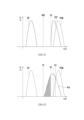
以下請參照圖2,圖2繪示本發明另一實施例的記憶體裝置的資料保存度的補償方法的流程圖。在步驟S210中,記憶體裝置的電源被開啟。在步驟S220中,記憶體裝置可針對已程式化記憶胞進行有無發生電荷損失現象的驗證動作。在此可同步參照圖2以及圖3A至圖3C繪示的記憶體裝置的資料保存度的補償動作的示意圖。在圖3A至圖3C中,橫軸表示記憶胞的臨界電壓的電壓值,縱軸表示記憶胞的數量。在圖3A中,記憶體裝置中的記憶胞的分佈曲線被區分為已抹區記憶胞分佈曲線ER以及已程式化記憶胞分佈曲線PGM。其中,已程式化記憶胞分佈曲線PGM中的記憶胞的臨界電壓均大於程式化驗證電壓VPV。針對各記憶胞以執行讀取動作的讀取參考電壓VRD則設置在已抹區記憶胞分佈曲線ER以及已程式化記憶胞分佈曲線PGM間,並與已程式化記憶胞分佈曲線PGM具有一足夠大的間距以作為一讀取邊界(read margin)。Please refer to Figure 2 below, which shows a flow chart of a method for compensating the data retention of a memory device according to another embodiment of the present invention. In step S210, the power of the memory device is turned on. In step S220, the memory device can perform a verification operation on the programmed memory cells to determine whether charge loss has occurred. Reference can be made here simultaneously to the schematic diagrams of the data retention compensation operation of the memory device shown in Figure 2 and Figures 3A to 3C. In Figures 3A to 3C, the horizontal axis represents the voltage value of the critical voltage of the memory cell, and the vertical axis represents the number of memory cells. In FIG3A , the distribution curve of the memory cells in the memory device is divided into an erased memory cell distribution curve ER and a programmed memory cell distribution curve PGM. The critical voltages of the memory cells in the programmed memory cell distribution curve PGM are all greater than the programming verification voltage VPV. The read reference voltage VRD for each memory cell to perform a read operation is set between the erased memory cell distribution curve ER and the programmed memory cell distribution curve PGM, and has a sufficiently large distance from the programmed memory cell distribution curve PGM to serve as a read margin.
在圖3B中,已程式化記憶胞分佈曲線PGM中部分的已程式化記憶胞可能因為環境因素、使用時間或被讀取次數等因素的至少其中之一而產生電荷損失的現象,而產生已程式化記憶胞分佈曲線310。此時,透過執行步驟S220,記憶體裝置中的控制器可設置第一閾值電壓V1以及第二閾值電壓V2,並透過針對已程式化記憶胞進行讀取動作,來判斷出臨界電壓介於第一閾值電壓V1以及第二閾值電壓V2的多個電荷損失記憶胞320。In FIG3B , some of the programmed memory cells in the programmed memory cell distribution curve PGM may have charge loss due to at least one of environmental factors, usage time, or read times, thereby generating a programmed memory
請重新參照圖2,在步驟S230中,當步驟S220的驗證動作為通過時(表示被驗證的已程式化記憶胞非為電荷損失記憶胞),可執行步驟S230以執行正常動作。Please refer to FIG. 2 again. In step S230, when the verification action of step S220 is passed (indicating that the verified programmed memory cell is not a charge loss memory cell), step S230 may be executed to perform normal actions.
當步驟S220的驗證動作為失敗時(表示被驗證的已程式化記憶胞為電荷損失記憶胞),可執行步驟S240,以針對電荷損失記憶胞執行補充程式化動作。When the verification action of step S220 fails (indicating that the verified programmed memory cell is a charge loss memory cell), step S240 may be executed to perform a supplementary programming action on the charge loss memory cell.
關於補充程式化動作的細節,請參照圖3C,承繼圖3B的實施方式,當記憶體裝置的控制器判斷出電荷損失記憶胞320後,控制器可針對電荷損失記憶胞320執行補充程式化動作。其中,控制器可設定等於第二閾值電壓V2的程式化驗證電壓,並透過提供具有程式化電壓的一個脈波至電荷損失記憶胞320來對電荷損失記憶胞320進行補充程式化動作,在此,上述程式化電壓可大於第二閾值電壓V2。或者,控制器可透過提供多個具有遞增電壓的脈波,透過遞增步階脈衝程式化的機制,對電荷損失記憶胞320執行補充程式化動作。For details of the supplementary programming action, please refer to FIG. 3C . Following the implementation of FIG. 3B , when the controller of the memory device determines that the charge
在完成補充程式化動作後,可獲得已程式化記憶胞的分佈曲線310’。After completing the supplementary programming action, the distribution curve 310' of the programmed memory cells can be obtained.
以下請參照圖4A以及圖4B,圖4A以及圖4B繪示本發明實施例的記憶體裝置的資料保存度的補償動作的另一實施方式的示意圖。在圖4A中,記憶體裝置的控制器可設定第一閾值電壓V1、第二閾值電壓V2以及第三閾值電壓V3,來對已程式化記憶胞分佈曲線410中的各個已程式化記憶胞進行驗證動作,其中第三閾值電壓V3大於第二閾值電壓V2,且第二閾值電壓V2大於第一閾值電壓V1。記憶體裝置的控制器根據第一閾值電壓V1、第二閾值電壓V2以及第三閾值電壓V3來針對各個已程式化記憶胞進行讀取動作,並藉以驗證出臨界電壓介於第一閾值電壓V1以及第三閾值電壓V3間的多個電荷損失記憶胞。Please refer to FIG. 4A and FIG. 4B below, which are schematic diagrams showing another implementation of the data retention compensation action of the memory device of the embodiment of the present invention. In FIG. 4A, the controller of the memory device can set the first threshold voltage V1, the second threshold voltage V2 and the third threshold voltage V3 to perform a verification action on each programmed memory cell in the programmed memory
在圖4B中,記憶體裝置的控制器可設定等於第三閾值電壓V3的程式化驗證電壓,並基於所設定的程式化驗證電壓來對電荷損失記憶胞進行補充程式化動作。透過針對電荷損失記憶胞執行電荷補充的動作,可產生新的已程式化記憶胞分佈曲線410’。In FIG4B , the controller of the memory device may set a programming verification voltage equal to the third threshold voltage V3, and perform a replenishment programming action on the charge loss memory cells based on the set programming verification voltage. By performing the charge replenishment action on the charge loss memory cells, a new programmed memory cell distribution curve 410 ' may be generated.
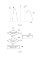
以下請參照圖5以及圖6,圖5以及圖6分別繪示本發明實施例的資料保存的補償動作的不同實施方式的流程圖。在圖5中,在步驟S510中,記憶體裝置可透過控制器以根據第二閾值電壓V2,在搭配錯誤檢查以及糾正(Error Checking and Correction, ECC)的機制的條件下,來針對已程式化記憶胞進行讀取動作。若上述的讀取動作為通過,表示已程式化記憶胞沒有發生嚴重的電荷損失的現象,而可以正常運作(步驟S530)。若步驟S510的讀取動作為失敗時,可執行步驟S520,記憶體裝置可透過控制器以根據第一閾值電壓V1以及第三閾值電壓V3來對已程式化記憶胞進行讀取動作。其中,第三閾值電壓V3大於第二閾值電壓V2,第二閾值電壓V2大於第一閾值電壓V1。Please refer to FIG. 5 and FIG. 6 below, which are flowcharts of different implementation methods of the data storage compensation action of the embodiment of the present invention. In FIG. 5, in step S510, the memory device can read the programmed memory cell through the controller according to the second threshold voltage V2 under the condition of the error checking and correction (ECC) mechanism. If the above-mentioned reading action is passed, it means that the programmed memory cell has not suffered from serious charge loss and can operate normally (step S530). If the reading action of step S510 fails, step S520 may be executed, and the memory device may read the programmed memory cell according to the first threshold voltage V1 and the third threshold voltage V3 through the controller. The third threshold voltage V3 is greater than the second threshold voltage V2, and the second threshold voltage V2 is greater than the first threshold voltage V1.
若已程式化記憶胞的臨界電壓介於第一閾值電壓V1以及第三閾值電壓V3間時,則步驟S520的讀取結果為失敗,相對的,若已程式化記憶胞的臨界電壓不介於第一閾值電壓V1以及第三閾值電壓V3間時,則步驟S520的讀取結果為通過。當步驟S520的讀取結果為失敗時,可執行步驟S540;相對的,當步驟S520的讀取結果為通過時,可執行步驟S530。If the critical voltage of the programmed memory cell is between the first threshold voltage V1 and the third threshold voltage V3, the reading result of step S520 is a failure. Conversely, if the critical voltage of the programmed memory cell is not between the first threshold voltage V1 and the third threshold voltage V3, the reading result of step S520 is a pass. When the reading result of step S520 is a failure, step S540 may be executed; conversely, when the reading result of step S520 is a pass, step S530 may be executed.
在步驟S540中,記憶體控制器可針對臨界電壓介於第一閾值電壓V1以及第三閾值電壓V3間的電荷損失記憶胞來執行補充程式化動作,並藉以對電荷損失記憶胞執行電荷的再填補動作。In step S540, the memory controller may perform a replenishment programming operation for the charge-loss memory cell whose critical voltage is between the first threshold voltage V1 and the third threshold voltage V3, thereby performing a charge refill operation on the charge-loss memory cell.
在圖6中,在步驟S610中,記憶體裝置可透過控制器以根據第一閾值電壓V1以及第二閾值電壓V2,在不搭配錯誤檢查以及糾正(ECC)的機制的條件下,來針對已程式化記憶胞進行讀取動作。若上述的讀取動作為通過,表示已程式化記憶胞沒有發生嚴重的電荷損失的現象,而可以正常運作(步驟S630)。若步驟S610的讀取動作為失敗時,可執行步驟S620,記憶體裝置可透過控制器以根據第三閾值電壓V3來對已程式化記憶胞進行讀取動作。其中,第三閾值電壓V3大於第二閾值電壓V2,第二閾值電壓V2大於第一閾值電壓V1。In FIG6 , in step S610, the memory device can read the programmed memory cell through the controller according to the first threshold voltage V1 and the second threshold voltage V2 without the use of an error checking and correction (ECC) mechanism. If the above-mentioned reading action is passed, it means that the programmed memory cell does not suffer from serious charge loss and can operate normally (step S630). If the reading action of step S610 fails, step S620 can be executed, and the memory device can read the programmed memory cell through the controller according to the third threshold voltage V3. The third threshold voltage V3 is greater than the second threshold voltage V2, and the second threshold voltage V2 is greater than the first threshold voltage V1.
透過步驟S620的讀取結果,可以驗證出臨界電壓介於第一閾值電壓V1以及第三閾值電壓V3間的電荷損失記憶胞。在步驟S640中,記憶體控制器可針對臨界電壓介於第一閾值電壓V1以及第三閾值電壓V3間的電荷損失記憶胞來執行補充程式化動作,並藉以對電荷損失記憶胞執行電荷的再填補動作。Through the reading result of step S620, the charge loss memory cell whose critical voltage is between the first threshold voltage V1 and the third threshold voltage V3 can be verified. In step S640, the memory controller can perform a supplement programming action for the charge loss memory cell whose critical voltage is between the first threshold voltage V1 and the third threshold voltage V3, and thereby perform a charge refill action on the charge loss memory cell.
以下請參照圖7,圖7繪示本發明一實施例的記憶體裝置的示意圖。記憶體裝置700包括記憶體區塊710以及控制器720。記憶體區塊710以及控制器720相互耦接。控制器720用以針對記憶體區塊710執行如前述多個實施例以及實施方式中所提及的已程式化記憶胞的資料保存度的補償方法。相關的動作細節在前述的實施例以及實施方式都已有詳細的說明,以下恕不多贅述。Please refer to FIG. 7 below, which is a schematic diagram of a memory device of an embodiment of the present invention. The
值得一提的,在本發明實施例中,記憶體區塊710可以為及式(AND)或反或式(NOR)快閃記憶體區塊。其中,記憶體區塊710可以為二維或三維式記憶體區塊。記憶體區塊710可具有多個分區。各個分區並可根據記憶胞的寫入狀態,被區分為已抹除記憶胞區塊以及已程式化記憶胞區塊。It is worth mentioning that in the embodiment of the present invention, the
另外,控制器720可以為具運算能力的處理器。或者,控制器720可以是透過硬體描述語言(Hardware Description Language, HDL)或是其他任意本領域具通常知識者所熟知的數位電路的設計方式來進行設計,並透過現場可程式邏輯門陣列(Field Programmable Gate Array, FPGA)、複雜可程式邏輯裝置(Complex Programmable Logic Device, CPLD)或是特殊應用積體電路(Application-specific Integrated Circuit, ASIC)的方式來實現的硬體電路,沒有特定的限制。In addition, the
以下請參照圖8,圖8繪示本發明一實施例的記憶體裝置的記憶胞的架構示意圖。在本發明實施例的記憶體裝置中,記憶胞區塊中的多個記憶胞MCs可以堆疊的方式來建構,並形成一三維架構的記憶胞串。每一記憶胞可具有氧化矽-氮化矽-氧化矽層ONO以作為絕緣層。並具有通道結構CH以及閘極結構GS。區域位元線BL以及區域源極線SL,分別透過導電插銷PG1、PG2以連接至記憶胞串中的全部記憶胞MCs。Please refer to FIG8 below, which shows a schematic diagram of the architecture of a memory cell of a memory device of an embodiment of the present invention. In the memory device of the embodiment of the present invention, multiple memory cells MCs in a memory cell block can be constructed in a stacked manner to form a memory cell string with a three-dimensional structure. Each memory cell may have a silicon oxide-silicon nitride-silicon oxide layer ONO as an insulating layer. And it has a channel structure CH and a gate structure GS. The regional bit line BL and the regional source line SL are connected to all the memory cells MCs in the memory cell string through conductive pins PG1 and PG2, respectively.
綜上所述,本發明的記憶體裝置透過讀取動作來判斷已程式化記憶胞有無發生電荷損失的現象。並透過補充程式化動作,來針對電荷損失記憶胞進行電荷的再填補動作,可有效維持記憶胞的資料保存度,確保資料的正確性。In summary, the memory device of the present invention determines whether the programmed memory cell has charge loss through the reading action. And through the supplementary programming action, the charge is refilled for the charge-loss memory cell, which can effectively maintain the data preservation of the memory cell and ensure the accuracy of the data.
310、310’、410、410’:已程式化記憶胞分佈曲線 320:電荷損失記憶胞 700:記憶體裝置 710:記憶體區塊 720:控制器 BL:區域位元線 CH:通道結構 ER:已抹區記憶胞分佈曲線 GS:閘極結構 MCs:記憶胞 ONO:氧化矽-氮化矽-氧化矽層 PG1、PG2:導電插銷 PGM:已程式化記憶胞分佈曲線 S110~S130、S210~S230、S510~S540、S610~S640:步驟 SL:區域源極線 V1~V3:閾值電壓 VPV:程式化驗證電壓 VRD:讀取參考電壓 310, 310', 410, 410': Programmed memory cell distribution curve 320: Charge loss memory cell 700: Memory device 710: Memory block 720: Controller BL: Regional bit line CH: Channel structure ER: Erased memory cell distribution curve GS: Gate structure MCs: Memory cell ONO: Silicon oxide-silicon nitride-silicon oxide layer PG1, PG2: Conductive pins PGM: Programmed memory cell distribution curve S110~S130, S210~S230, S510~S540, S610~S640: Steps SL: Local source line V1~V3: Threshold voltage VPV: Programming verification voltage VRD: Read reference voltage
圖1繪示本發明一實施例的資料保存度的補償方法的流程圖。 圖2繪示本發明另一實施例的記憶體裝置的資料保存度的補償方法的流程圖。 圖3A至圖3C繪示記憶體裝置的資料保存度的補償動作的示意圖。 圖4A以及圖4B繪示本發明實施例的記憶體裝置的資料保存度的補償動作的另一實施方式的示意圖。 圖5以及圖6分別繪示本發明實施例的資料保存的補償動作的不同實施方式的流程圖。 圖7繪示本發明一實施例的記憶體裝置的示意圖。 圖8繪示本發明一實施例的記憶體裝置的記憶胞的架構示意圖。 FIG. 1 is a flowchart of a method for compensating data preservation of an embodiment of the present invention. FIG. 2 is a flowchart of a method for compensating data preservation of a memory device of another embodiment of the present invention. FIG. 3A to FIG. 3C are schematic diagrams of a compensation action for data preservation of a memory device. FIG. 4A and FIG. 4B are schematic diagrams of another implementation of a compensation action for data preservation of a memory device of an embodiment of the present invention. FIG. 5 and FIG. 6 are flowcharts of different implementations of a compensation action for data preservation of an embodiment of the present invention, respectively. FIG. 7 is a schematic diagram of a memory device of an embodiment of the present invention. FIG8 is a schematic diagram showing the structure of a memory cell of a memory device according to an embodiment of the present invention.
S110~S130:步驟S110~S130: Steps
Claims (18)
Priority Applications (1)
| Application Number | Priority Date | Filing Date | Title |
|---|---|---|---|
| TW112108611A TWI856552B (en) | 2023-03-09 | 2023-03-09 | Memory device and compensation method of data retention thereof |
Applications Claiming Priority (1)
| Application Number | Priority Date | Filing Date | Title |
|---|---|---|---|
| TW112108611A TWI856552B (en) | 2023-03-09 | 2023-03-09 | Memory device and compensation method of data retention thereof |
Publications (2)
| Publication Number | Publication Date |
|---|---|
| TW202437262A TW202437262A (en) | 2024-09-16 |
| TWI856552B true TWI856552B (en) | 2024-09-21 |
Family
ID=93609494
Family Applications (1)
| Application Number | Title | Priority Date | Filing Date |
|---|---|---|---|
| TW112108611A TWI856552B (en) | 2023-03-09 | 2023-03-09 | Memory device and compensation method of data retention thereof |
Country Status (1)
| Country | Link |
|---|---|
| TW (1) | TWI856552B (en) |
Citations (4)
| Publication number | Priority date | Publication date | Assignee | Title |
|---|---|---|---|---|
| US5768193A (en) * | 1996-06-17 | 1998-06-16 | Aplus Integrated Circuits, Inc. | Bit-refreshable method and circuit for refreshing a nonvolatile flash memory |
| US6493270B2 (en) * | 1999-07-01 | 2002-12-10 | Micron Technology, Inc. | Leakage detection in programming algorithm for a flash memory device |
| EP3404661A1 (en) * | 2016-03-09 | 2018-11-21 | Huawei Technologies Co., Ltd. | Flash memory device refreshing method and apparatus |
| TW202221901A (en) * | 2020-11-25 | 2022-06-01 | 美商英飛淩科技有限責任公司 | Silicon-oxide-nitride-oxide-silicon based multi-level non-volatile memory device and methods of operation thereof |
-
2023
- 2023-03-09 TW TW112108611A patent/TWI856552B/en active
Patent Citations (5)
| Publication number | Priority date | Publication date | Assignee | Title |
|---|---|---|---|---|
| US5768193A (en) * | 1996-06-17 | 1998-06-16 | Aplus Integrated Circuits, Inc. | Bit-refreshable method and circuit for refreshing a nonvolatile flash memory |
| US6493270B2 (en) * | 1999-07-01 | 2002-12-10 | Micron Technology, Inc. | Leakage detection in programming algorithm for a flash memory device |
| US6650585B2 (en) * | 1999-07-01 | 2003-11-18 | Micron Technology, Inc. | Leakage detection in programming algorithm for a flash memory device |
| EP3404661A1 (en) * | 2016-03-09 | 2018-11-21 | Huawei Technologies Co., Ltd. | Flash memory device refreshing method and apparatus |
| TW202221901A (en) * | 2020-11-25 | 2022-06-01 | 美商英飛淩科技有限責任公司 | Silicon-oxide-nitride-oxide-silicon based multi-level non-volatile memory device and methods of operation thereof |
Also Published As
| Publication number | Publication date |
|---|---|
| TW202437262A (en) | 2024-09-16 |
Similar Documents
| Publication | Publication Date | Title |
|---|---|---|
| US11430531B2 (en) | Read integration time calibration for non-volatile storage | |
| CN109712664B (en) | Memory device including circuit for detecting word line defects and method of operating the same | |
| US11164634B2 (en) | Non-volatile storage system with fast SLC operation | |
| KR102069864B1 (en) | Semiconductor memory device and operating method thereof | |
| US7826274B2 (en) | Non-volatile memory cell read failure reduction | |
| US9009568B2 (en) | Sensing parameter management in non-volatile memory storage system to compensate for broken word lines | |
| US11373710B1 (en) | Time division peak power management for non-volatile storage | |
| US10482973B2 (en) | Memory devices including a word line defect detection circuit | |
| US12046314B2 (en) | NAND memory with different pass voltage ramp rates for binary and multi-state memory | |
| CN106205702B (en) | Non-volatile memory device automatically responding to program failure | |
| US11670380B2 (en) | Two-sided adjacent memory cell interference mitigation | |
| US20230124035A1 (en) | Non-volatile memory with pre-trained model and inference circuit | |
| US11875043B1 (en) | Loop dependent word line ramp start time for program verify of multi-level NAND memory | |
| US11114178B1 (en) | Physical defect detection in an integrated memory assembly | |
| CN118318272A (en) | Efficient testing of nonvolatile memories during erase | |
| TWI856552B (en) | Memory device and compensation method of data retention thereof | |
| US11514991B1 (en) | Program tail plane comparator for non-volatile memory structures | |
| CN115881179A (en) | Storage device and method of operating storage device | |
| US12614598B2 (en) | Fake fast plane detection in early program termination | |
| US12374402B2 (en) | Smart early program termination algorithm for neighbor plane disturb countermeasure | |
| US12488846B2 (en) | Negative word line enabled pre-boosting strategy to improve NAND program performance | |
| CN118626000A (en) | Memory device and data retention compensation method thereof | |
| US12148489B2 (en) | Early detection of programming failure for non-volatile memory | |
| US12040031B2 (en) | Non-volatile memory with autonomous cycling | |
| US12334160B2 (en) | Apparatus and method for detecting neighbor plane erase failures |