TWI729552B - Operating circuit - Google Patents
Operating circuit Download PDFInfo
- Publication number
- TWI729552B TWI729552B TW108139843A TW108139843A TWI729552B TW I729552 B TWI729552 B TW I729552B TW 108139843 A TW108139843 A TW 108139843A TW 108139843 A TW108139843 A TW 108139843A TW I729552 B TWI729552 B TW I729552B
- Authority
- TW
- Taiwan
- Prior art keywords
- power
- normally open
- voltage
- open switch
- signal
- Prior art date
Links
Images


Classifications
-
- H—ELECTRICITY
- H03—ELECTRONIC CIRCUITRY
- H03K—PULSE TECHNIQUE
- H03K17/00—Electronic switching or gating, i.e. not by contact-making and –breaking
- H03K17/51—Electronic switching or gating, i.e. not by contact-making and –breaking characterised by the components used
- H03K17/56—Electronic switching or gating, i.e. not by contact-making and –breaking characterised by the components used by the use, as active elements, of semiconductor devices
- H03K17/687—Electronic switching or gating, i.e. not by contact-making and –breaking characterised by the components used by the use, as active elements, of semiconductor devices the devices being field-effect transistors
- H03K17/6871—Electronic switching or gating, i.e. not by contact-making and –breaking characterised by the components used by the use, as active elements, of semiconductor devices the devices being field-effect transistors the output circuit comprising more than one controlled field-effect transistor
-
- H—ELECTRICITY
- H03—ELECTRONIC CIRCUITRY
- H03K—PULSE TECHNIQUE
- H03K17/00—Electronic switching or gating, i.e. not by contact-making and –breaking
- H03K17/51—Electronic switching or gating, i.e. not by contact-making and –breaking characterised by the components used
- H03K17/56—Electronic switching or gating, i.e. not by contact-making and –breaking characterised by the components used by the use, as active elements, of semiconductor devices
- H03K17/687—Electronic switching or gating, i.e. not by contact-making and –breaking characterised by the components used by the use, as active elements, of semiconductor devices the devices being field-effect transistors
- H03K17/693—Switching arrangements with several input- or output-terminals, e.g. multiplexers, distributors
-
- H—ELECTRICITY
- H02—GENERATION; CONVERSION OR DISTRIBUTION OF ELECTRIC POWER
- H02J—ELECTRIC POWER NETWORKS; CIRCUIT ARRANGEMENTS OR SYSTEMS FOR SUPPLYING OR DISTRIBUTING ELECTRIC POWER; SYSTEMS FOR STORING ELECTRIC ENERGY
- H02J7/00—Circuit arrangements for charging or discharging batteries or for supplying loads from batteries
- H02J7/855—Circuit arrangements for charging or discharging batteries or for supplying loads from batteries with circuits adapted for supplying loads from the battery
-
- H—ELECTRICITY
- H02—GENERATION; CONVERSION OR DISTRIBUTION OF ELECTRIC POWER
- H02J—ELECTRIC POWER NETWORKS; CIRCUIT ARRANGEMENTS OR SYSTEMS FOR SUPPLYING OR DISTRIBUTING ELECTRIC POWER; SYSTEMS FOR STORING ELECTRIC ENERGY
- H02J3/00—Circuit arrangements for AC mains or AC distribution networks
- H02J3/007—Arrangements for selectively connecting one or more loads to one or more power sources or power lines
-
- H—ELECTRICITY
- H02—GENERATION; CONVERSION OR DISTRIBUTION OF ELECTRIC POWER
- H02J—ELECTRIC POWER NETWORKS; CIRCUIT ARRANGEMENTS OR SYSTEMS FOR SUPPLYING OR DISTRIBUTING ELECTRIC POWER; SYSTEMS FOR STORING ELECTRIC ENERGY
- H02J4/00—Circuit arrangements for mains or distribution networks not specified as AC or DC; Circuit arrangements for mains or distribution networks combining AC and DC sections or sub-networks
-
- H—ELECTRICITY
- H02—GENERATION; CONVERSION OR DISTRIBUTION OF ELECTRIC POWER
- H02J—ELECTRIC POWER NETWORKS; CIRCUIT ARRANGEMENTS OR SYSTEMS FOR SUPPLYING OR DISTRIBUTING ELECTRIC POWER; SYSTEMS FOR STORING ELECTRIC ENERGY
- H02J7/00—Circuit arrangements for charging or discharging batteries or for supplying loads from batteries
- H02J7/34—Parallel operation in networks using both storage and other DC sources, e.g. providing buffering
-
- H—ELECTRICITY
- H03—ELECTRONIC CIRCUITRY
- H03K—PULSE TECHNIQUE
- H03K17/00—Electronic switching or gating, i.e. not by contact-making and –breaking
- H03K17/51—Electronic switching or gating, i.e. not by contact-making and –breaking characterised by the components used
- H03K17/56—Electronic switching or gating, i.e. not by contact-making and –breaking characterised by the components used by the use, as active elements, of semiconductor devices
- H03K17/687—Electronic switching or gating, i.e. not by contact-making and –breaking characterised by the components used by the use, as active elements, of semiconductor devices the devices being field-effect transistors
- H03K2017/6875—Electronic switching or gating, i.e. not by contact-making and –breaking characterised by the components used by the use, as active elements, of semiconductor devices the devices being field-effect transistors using self-conductive, depletion FETs
Landscapes
- Engineering & Computer Science (AREA)
- Power Engineering (AREA)
- Direct Current Feeding And Distribution (AREA)
Abstract
Description
本發明係有關於一種操作電路,特別是有關於一種可接收多電源輸入的操作電路。The present invention relates to an operating circuit, and more particularly, to an operating circuit that can receive multiple power inputs.
一般的電子裝置僅具有單一電源埠,用以接收外部電源。然而,當使用者忘記攜帶充電線時,便無法對電子裝置充電。再者,就算使用者將充電線插入電子裝置時,如果使用者無預警地拔除充電線時,則電子裝置會直接斷電,可能造成內部元件的損壞。General electronic devices only have a single power port for receiving external power. However, when the user forgets to carry the charging cable, the electronic device cannot be charged. Furthermore, even when the user inserts the charging cable into the electronic device, if the user unplugs the charging cable without warning, the electronic device will be directly powered off, which may cause damage to internal components.
本發明提供一種操作電路,包括一系統電路以及一電源控制電路。系統電路根據一節點的電源而動作。電源控制電路包括一第一連接埠、一第二連接埠、一第一常開開關、一第二常開開關、一第一限流器以及一第二限流器。第一連接埠用以接收一第一外部裝置所提供的一第一電源。第二連接埠用以接收一第二外部裝置所提供的一第二電源。第一常開開關耦接第一連接埠,用以傳送第一電源。第二常開開關耦接第二連接埠,用以傳送第二電源。第一限流器耦接於第一常開開關與節點之間,用以提供第一電源予節點。第二限流器耦接於第二常開開關與節點之間,用以提供第二電源予節點。當第一及第二連接埠分別耦接第一及第二外部裝置時,系統電路與第一及第二外部裝置溝通,用以得知第一及第二電源的特性,並根據第一及第二電源的特性,命令第一或第二常開開關停止傳送第一或第二電源。The present invention provides an operating circuit including a system circuit and a power control circuit. The system circuit operates according to the power supply of a node. The power control circuit includes a first connection port, a second connection port, a first normally open switch, a second normally open switch, a first current limiter and a second current limiter. The first connection port is used for receiving a first power source provided by a first external device. The second connection port is used for receiving a second power source provided by a second external device. The first normally open switch is coupled to the first connection port for transmitting the first power. The second normally open switch is coupled to the second connection port for transmitting the second power. The first current limiter is coupled between the first normally open switch and the node for providing the first power to the node. The second current limiter is coupled between the second normally open switch and the node for providing the second power to the node. When the first and second connection ports are respectively coupled to the first and second external devices, the system circuit communicates with the first and second external devices to learn the characteristics of the first and second power supplies, and according to the first and second external devices The characteristics of the second power source, command the first or second normally open switch to stop transmitting the first or second power source.
為讓本發明之目的、特徵和優點能更明顯易懂,下文特舉出實施例,並配合所附圖式,做詳細之說明。本發明說明書提供不同的實施例來說明本發明不同實施方式的技術特徵。其中,實施例中的各元件之配置係為說明之用,並非用以限制本發明。另外,實施例中圖式標號之部分重覆,係為了簡化說明,並非意指不同實施例之間的關聯性。In order to make the purpose, features and advantages of the present invention more comprehensible, embodiments are specifically listed below, and detailed descriptions are made in conjunction with the accompanying drawings. The specification of the present invention provides different examples to illustrate the technical features of different embodiments of the present invention. Wherein, the configuration of each element in the embodiment is for illustrative purposes, and is not intended to limit the present invention. In addition, the part of the repetition of the symbols of the drawings in the embodiments is for simplifying the description, and does not imply the relevance between different embodiments.
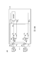
第1圖為本發明之操作系統的示意圖。如圖所示,操作系統100包括外部裝置110、120及一操作電路130。外部裝置110用以提供電源PW予操作電路130。外部裝置120用以提供電源PW
2予操作電路130。在本實施例中,電源PW
1及PW
2係為直流電源。本發明並不限定外部裝置110及120的種類。在一可能實施例中,外部裝置110及120係為交流-直流轉換器(AC to DC converter)。在其它實施例中,外部裝置110及120係為直流轉換器(DC converter)。
Figure 1 is a schematic diagram of the operating system of the present invention. As shown in the figure, the
操作電路130包括一電源控制電路131以及一系統電路132。電源控制電路131用以供電予系統電路132。系統電路132根據電源控制電路131所提供的電源而動作。在本實施例中,電源控制電路131所提供的電源係為系統電路132的工作電源。如圖所示,電源控制電路131包括連接埠IN
1及IN
2、常開開關(always on)SW
1及SW
2以及限流器D
1及D
2。
The
連接埠IN 1及IN 2分別具有電源接腳P P1及P P2。電源接腳P P1用以接收電源PW 1。電源接腳P P2用以接收電源PW 2。本發明並不限定連接埠IN 1及IN 2的種類。以連接埠IN 1為例,在一可能實施例中,連接埠IN 1係為USB Type-C連接埠。在此例中,USB Type-C連接埠的VBUS接腳作為電源接腳P P1。在其它實施例中,連接埠IN 1係為一USB Mini-A連接埠、一USB Mini-B連接埠、一USB Micro-A連接埠或是一USB Micro-B連接埠。在此例中,USB Mini-A連接埠、USB Mini-B連接埠、USB Micro-A連接埠或是USB Micro-B連接埠的VBUS接腳作為電源接腳P P1。 The connection ports IN 1 and IN 2 have power pins P P1 and P P2 respectively . The power pin P P1 is used to receive the power PW 1 . The power pin P P2 is used to receive the power PW 2 . The invention does not limit the types of the connection ports IN 1 and IN 2. Taking the port IN 1 as an example, in a possible embodiment, the port IN 1 is a USB Type-C port. In this example, the VBUS pin of the USB Type-C port is used as the power pin P P1 . In other embodiments, the port IN 1 is a USB Mini-A port, a USB Mini-B port, a USB Micro-A port, or a USB Micro-B port. In this example, the VBUS pin of the USB Mini-A port, USB Mini-B port, USB Micro-A port, or USB Micro-B port is used as the power pin P P1 .
在其它實施例中,連接埠IN
1及IN
2更具有溝通接腳P
T1及P
T2。系統電路132透過溝通接腳P
T1及P
T2與外部裝置110及120溝通,用以得知電源PW
1及PW
2的特性(如電壓成分及電流成分)。系統電路132根據電源PW
1及PW
2的特性,產生關閉信號Toff
1及Toff
2,用以命令電源控制電路131提供電源PW
1及PW
2之至少一者。
In other embodiments, the connection ports IN 1 and IN 2 further have communication pins P T1 and P T2 . The
舉例而言,當電源PW
1的電壓成分高於電源PW
2的電壓成分(如電源PW
1的電壓成分為20V,電源PW
2的電壓成分為12V)時,系統電路132要求電源控制電路131提供電源PW
1。在另一可能實施例中,當電源PW
1的電流成分低於電源PW
2的電源成分時(如電源PW
1的電流成分為1A,電源PW
2的電流成分為3A),系統電路132要求電源控制電路131提供電源PW
2。在其它實施例中,當電源PW
1的電壓成分相同於電源PW
2的電源成分時,系統電路132可能要求電源控制電路131同時提供電源PW
1及PW
2。
For example, when the voltage component of the power supply PW 1 is higher than the voltage component of the power supply PW 2 (for example , the voltage component of the power supply PW 1 is 20V, and the voltage component of the power supply PW 2 is 12V), the
由於電源控制電路131具有連接埠IN
1及IN
2,故不論是連接埠IN
1接收到電源PW
1或是連接埠IN
2接收到電源PW
2,系統電路132都可以根據電源PW
1及PW
2之至少一者而動作。因此,增加操作系統100的便利性。
Since the
常開開關SW
1及SW
2分別耦接連接埠IN
1及IN
2,用以傳送電源PW
1及PW
2。由於常開開關SW
1及SW
2的特性相同,故僅以常開開關SW
1為例,說明常開開關SW
1的動作方式。如圖所示,常開開關SW
1具有端點A、B及C。端點A耦接連接埠IN
1的電源接腳P
P1。端點B耦接限流器D
1。端點C接收關閉信號Toff
1。當關閉信號Toff
1未被致能時,端點A接觸端點B。因此,當外部裝置110耦接連接埠IN
1時,常開開關SW
1傳送電源PW
1予限流器D
1。當關閉信號Toff
1被致能時,端點A接觸端點C。因此,常開開關SW
1停止傳送電源PW
1予限流器D
1。在本實施例中,端點A常接觸端點B。因此,只要關閉信號Toff
1未被致能,常開開關SW
1持續傳送電源PW
1予限流器D
1。
The normally open switches SW 1 and SW 2 are respectively coupled to the connection ports IN 1 and IN 2 for transmitting power PW 1 and PW 2 . Since the characteristics of the normally open switch SW 1 and SW 2 are the same, only the normally open switch SW 1 is taken as an example to illustrate the operation mode of the normally open switch SW 1. As illustrated, normally open out switch SW 1 has an end point A, B and C. The terminal A is coupled to the power pin P P1 of the port IN 1 . The terminal B is coupled to the current limiter D 1 . Endpoint C receives the off signal Toff 1 . When the off signal Toff 1 is not enabled, the terminal A contacts the terminal B. Therefore, when the
由於常開開關SW
1及SW
2的端點A常接觸端點B,故可持續供電予系統電路132,使得系統電路132正常工作。再者,操作電路130不需接收來自外部的致能信號,便可供電予系統電路132。
Since the terminal A of the normally open switches SW 1 and SW 2 always contact the terminal B, the
限流器D 1耦接於常開開關SW 1與節點ND之間,用以提供電源PW 1予節點ND。在本實施例中,限流器D 1係為一二極體,用以避免節點ND的電流反饋至常開開關SW 1。限流器D 2耦接於常開開關SW 2與節點ND之間,用以提供電源PW 2予節點ND。在本實施例中,限流器D 2係為一二極體,用以避免節點ND的電流反饋進入常開開關SW 2。 The current limiter D 1 is coupled between the normally open switch SW 1 and the node ND to provide the power PW 1 to the node ND. In this embodiment, the current limiter D 1 is a diode to prevent the current at the node ND from being fed back to the normally open switch SW 1 . The current limiter D 2 is coupled between the normally open switch SW 2 and the node ND for providing power PW 2 to the node ND. In this embodiment, the current limiter D 2 is a diode to prevent the current at the node ND from being fed back into the normally open switch SW 2 .
在其它實施例中,電源控制電路131更包括電阻R
1及R
2。如圖所示,電阻R
1耦接於常開開關SW
1與系統電路132之間,用以傳送關閉信號Toff
1予常開開關SW
1。電阻R
2耦接於常開開關SW
2與系統電路132之間,用以提供關閉信號Toff
2予常開開關SW
2。
In other embodiments, the
在本實施例中,系統電路132根據電源PW
1及PW
2的特性,控制關閉信號Toff
1及Toff
2。舉例而言,如果系統電路132透過溝通接腳P
T1及P
T2得知電源PW
1係為一15V/1A電源,而電源PW
2係為一12V/3A電源。在此例中,由於電源PW
1的電壓成分大於電源PW
2的電壓成分,故系統電路132致能關閉信號Toff
2。因此,常開開關SW
2的端點A不再接觸端點B,用以停止傳送電源PW
2至節點ND。此時,由於關閉信號Toff
1未被致能,故常開開關SW
1的端點A仍然接觸端點B。因此,常開開關SW
1傳送電源PW
1至節點ND。由於常開開關的預設狀態係為一短路(short)狀態,故可持續傳送相對應的電源,而不需額外提供一致能信號予常開開關。
In the present embodiment, the characteristics of the
在另一可能實施例中,由於電源PW
2的電流成分大於電源PW
1的電流成分,故系統電路132致能關閉信號Toff
1。因此,常開開關SW
1的端點A不再接觸端點B,用以停止傳送電源PW
1至節點ND。此時,由於關閉信號Toff
2未被致能,故常開開關SW
2的端點A接觸端點B。因此,常開開關SW
2傳送電源PW
2至節點ND。
In another possible embodiment, since the current component of the power supply PW 2 is greater than the current component of the power supply PW 1 , the
在其它實施例中,如果電源PW
1係為一15V/1A電源,而電源PW
2係為一15V/3A電源。在此例中,系統電路132可能不致能關閉信號Toff
1及Toff
2。因此,常開開關SW
1及SW
2的端點A接觸端點B,用以傳送電源PW
1及PW
2至節點ND。
In other embodiments, if the power source PW 1 is a 15V/1A power source, and the power source PW 2 is a 15V/3A power source. In this example, the
第2圖為本發明之操作系統的另一示意圖。第2圖的操作系統200相似於第1圖的操作系統100,不同之處在於,第2圖的電源控制電路131更包括開關T
1、T
2及反相比較器CMP
1及CMP
2。另外,第2圖的系統電路132包括一電壓轉換電路210。電壓轉換電路210轉換節點ND的電壓,用以產生一轉換電壓V
T。在本實施例中,轉換電壓V
T作為一參考電壓Vref。本發明並不限定電壓轉換電路210的架構。在一可能實施例中,電壓轉換電路210係為一直流轉換器(DC-DC converter),用以增加或降低節點ND的電壓。在其它實施例中,電壓轉換電路210可能根據節點ND的電壓,產生多組轉換電壓,用以供不同電路(未顯示)使用。
Figure 2 is another schematic diagram of the operating system of the present invention. The
反相比較器CMP
1根據電源PW
2及參考電壓Vref,產生一開啟信號Ton
1。在本實施例中,反相比較器CMP
1比較電源PW
2與參考電壓Vref。當電源PW
2小於參考電壓Vref時,表示外部裝置120可能被移除,或是外部裝置120工作異常。因此,反相比較器CMP
1致能開啟信號Ton
1。當電源PW
2不小於參考電壓Vref時,表示外部裝置120提供穩定的電源。因此,反相比較器CMP
1不致能開啟信號Ton
1。
The inverting comparator CMP 1 generates a turn-on signal Ton 1 according to the power supply PW 2 and the reference voltage Vref. In this embodiment, the inverting comparator CMP 1 compares the power supply PW 2 with the reference voltage Vref. When the power supply PW 2 is less than the reference voltage Vref, it means that the
開關T
1根據開啟信號Ton
1控制常開開關SW
1。舉例而言,當開啟信號Ton
1被致能時,表示電源PW
2不穩定。因此,開關T
1導通,用以命令常開開關SW
1進入一開啟模式。在此模式下,常開開關SW
1的端點A接觸端點B,用以傳送電源PW
1予限流器D
1。然而,當開啟信號Ton
1未被致能時,表示外部裝置120正常供電。因此,開關T
1不導通。此時,常開開關SW
1根據關閉信號Toff
1而動作。舉例而言,如果關閉信號Toff
1被致能,表示系統電路132需要其它的電源。因此,常開開關SW
1根據被致能的關閉信號Toff
1進入一關閉模式。在關閉模式下,常開開關SW
1的端點A不接觸端點B。因此,常開開關SW
1停止傳送電源PW
1予限流器D
1。然而,如果關閉信號Toff
1未被致能,表示系統電路132需要電源PW
1。因此,常開開關SW
1根據未被致能的關閉信號Toff
1,操作於一開啟模式。在開啟模式下,常開開關SW
1的端點A接觸端點B,故持續傳送電源PW
1予限流器D
1。本發明並不限定開關T
1的種類。在一可能實施例中,開關T
1係為一N型電晶體。
T 1 is turned on in accordance with switch control signal Ton 1 normally open switch SW 1. For example, when the turn-on signal Ton 1 is enabled, it means that the power supply PW 2 is unstable. Therefore, the switch T 1 is turned on to command the normally open switch SW 1 to enter an on mode. In this mode, the terminal A of the normally open switch SW 1 contacts the terminal B to transmit the power PW 1 to the current limiter D 1 . However, when the turn-on signal Ton 1 is not enabled, it means that the
反相比較器CMP
2根據電源PW
1及參考電壓Vref,產生一開啟信號Ton
2。在本實施例中,反相比較器CMP
2比較電源PW
1與參考電壓Vref。當電源PW
1小於參考電壓Vref時,表示外部裝置110可能被移除,或是外部裝置110工作異常。因此,反相比較器CMP
2致能開啟信號Ton
2。當電源PW
1不小於參考電壓Vref時,表示外部裝置110提供穩定的電源。因此,反相比較器CMP
2不致能開啟信號Ton
2。
The inverting comparator CMP 2 generates a turn-on signal Ton 2 according to the power supply PW 1 and the reference voltage Vref. In this embodiment, the inverting comparator CMP 2 compares the power supply PW 1 with the reference voltage Vref. When the power supply PW 1 is less than the reference voltage Vref, it indicates that the
開關T
2根據開啟信號Ton
2控制常開開關SW
2。由於開關T
2的特性與開關T
1的特性相似,故不再贅述。由於反相比較器CMP
1及CMP
2監控電源PW
1及PW
2,故在電源PW
1或PW
2不穩定或小於一臨界值(如參考電壓Vref)時,反相比較器CMP
1或CMP
2即時命令相對應的常開開關進入一開啟模式。在開啟模式下,常開開關立即傳送電源,用以提供穩定的電源予節點ND,並維持系統電路132的運作。
The turn signal switch T 2 Ton 2 controls a normally open switch SW 2. Since the switching characteristics of the switch T 2 to T 1 of similar characteristics, and therefore it will not be repeated. Since the inverting comparators CMP 1 and CMP 2 monitor the power supplies PW 1 and PW 2 , when the power supply PW 1 or PW 2 is unstable or less than a critical value (such as the reference voltage Vref), the inverting comparator CMP 1 or CMP 2 The normally open switch corresponding to the immediate command enters an open mode. In the on mode, the normally open switch immediately transmits power to provide stable power to the node ND and maintain the operation of the
第3圖為本發明之操作系統的另一示意圖。第3圖的操作系統300相似於第2圖的操作系統200,不同之處在於第3圖的電源控制電路131更包括分壓電路DV
1及DV
2。
Figure 3 is another schematic diagram of the operating system of the present invention. The
分壓電路DV 1處理電源PW 2,用以產生電壓V 1。反相比較器CMP 1根據電壓V 1而動作。舉例而言,當電壓V 1小於參考電壓Vref時,反相比較器CMP 1致能開啟信號Ton 1。此時,開啟信號Ton 1可能為一高位準。當電壓V 1不小於參考電壓Vref時,反相比較器CMP 1不致能開啟信號Ton 1。此時,開啟信號Ton 1可能為一低位準。 The voltage divider circuit DV 1 processes the power supply PW 2 to generate the voltage V 1 . The inverting comparator CMP 1 operates in accordance with the voltage V 1 . For example, when the voltage V 1 is less than the reference voltage Vref, the inverting comparator CMP 1 enables the signal Ton 1 . At this time, the turn-on signal Ton 1 may be at a high level. When the voltage V 1 is not less than the reference voltage Vref, the inverting comparator CMP 1 cannot turn on the signal Ton 1 . At this time, the turn-on signal Ton 1 may be at a low level.
分壓電路DV 2處理電源PW 1,用以產生電壓V 2。反相比較器CMP 2根據電壓V 2而動作。由於反相比較器CMP 2的特性與反相比較器CMP 1的特性相似,故不再贅述。 The voltage divider circuit DV 2 processes the power supply PW 1 to generate the voltage V 2 . The inverting comparator CMP 2 operates according to the voltage V 2 . Since the characteristics of the comparator CMP inverter inverting comparator CMP 2 is a similar characteristic, it is omitted.
在其它實施例中,系統電路132更包括一電壓產生電路310。電壓產生電路310根據轉換電壓V
T,產生參考電壓Vref。本發明並不限定電壓產生電路310的架構。在一可能實施例中,電壓產生電路310係為一分壓電路。
In other embodiments, the
第4圖為本發明之操作系統的另一示意圖。第4圖的操作系統400相似於第2圖的操作系統200,不同之處在於,第4圖的操作系統400更包括一外部裝置410。外部裝置410用以提供電源PW
3。由於外部裝置410的特性與第2圖的外部裝置110的特性相似,故不再贅述。
Figure 4 is another schematic diagram of the operating system of the present invention. The
另外,在本實施例中,電源控制電路131更包括一連接埠IN
3、一常開開關SW
3、限流器D
3及421~426、一電阻R
3、一開關T
3、一反相比較器CMP
3。本發明並不限定電源控制電路131的連接埠的數量。當電源控制電路131具有更多連接埠時,便可接收更多的電源。此外,本發明亦不限定常開開關、限流器、電阻、開關及反相比較器的數量。在本實施例中,當連接埠的數量愈多時,常開開關、限流器、電阻、開關及反相比較器的數量也愈多。
In addition, in this embodiment, the
由於連接埠IN 3、常開開關SW 3、限流器D 3、電阻R 3、開關T 3、反相比較器CMP 3的特性與第2圖的連接埠IN 1、常開開關SW 1、限流器D 1、電阻R 1、開關T 1、反相比較器CMP 1的特性相似,故不再贅述。 Due to the characteristics of the port IN 3 , the normally open switch SW 3 , the current limiter D 3 , the resistor R 3 , the switch T 3 , and the inverting comparator CMP 3 , the characteristics of the port IN 1 and the normally open switch SW 1 , The characteristics of the current limiter D 1 , the resistor R 1 , the switch T 1 , and the inverting comparator CMP 1 are similar, so they will not be described again.
在本實施例中,限流器421的輸入端接收電源PW
2,其輸出端耦接反相比較器CMP
1的反相輸入端。此外,限流器422的輸入端接收電源PW
3,其輸出端耦接反相比較器CMP
1的反相輸入端。當電源PW
2大於電源PW
3時,反相比較器CMP
1比較電源PW
2與參考電壓Vref,用以產生開啟信號Ton
1。當電源PW
2小於電源PW
3時,反相比較器CMP
1比較電源PW
3與參考電壓Vref,用以產生開啟信號Ton
1。在其它實施例中,當電源PW
2與PW
3均小於參考電壓Vref時,反相比較器CMP
1致能開啟信號Ton
1。在本實施例中,限流器421用以避免電源PW
3反饋至外部裝置120,限流器422用以避免電源PW
2反饋至外部裝置410。
In this embodiment, the input terminal of the
限流器423的輸入端接收電源PW
1,其輸出端耦接反相比較器CMP
2的反相輸入端。此外,限流器424的輸入端接收電源PW
3,其輸出端耦接反相比較器CMP
2的反相輸入端。當電源PW
1大於電源PW
3時,反相比較器CMP
2比較電源PW
1與參考電壓Vref,用以產生開啟信號Ton
2。當電源PW
1小於電源PW
3時,反相比較器CMP
2比較電源PW
3與參考電壓Vref,用以產生開啟信號Ton
2。在其它實施例中,當電源PW
1與PW
3均小於參考電壓Vref時,反相比較器CMP
2致能開啟信號Ton
2。在本實施例中,限流器423用以避免電源PW
3反饋至外部裝置110,限流器424用以避免電源PW
1反饋至外部裝置410。
The input terminal of the
限流器425的輸入端接收電源PW
1,其輸出端耦接反相比較器CMP
3的反相輸入端。此外,限流器426的輸入端接收電源PW
2,其輸出端耦接反相比較器CMP
3的反相輸入端。當電源PW
1大於電源PW
2時,反相比較器CMP
3比較電源PW
1與參考電壓Vref,用以產生開啟信號Ton
3。當電源PW
1小於電源PW
2時,反相比較器CMP
3比較電源PW
2與參考電壓Vref,用以產生開啟信號Ton
3。在其它實施例中,當電源PW
1與PW
2均小於參考電壓Vref時,反相比較器CMP
3致能開啟信號Ton
3。在本實施例中,限流器425用以避免電源PW
2饋至外部裝置110,限流器426用以避免電源PW
1反饋至外部裝置120。
The input terminal of the
在其它實施例中,限流器421及422的輸出端耦接一第一分壓電路(未顯示)。第一分壓電路對限流器421及422的輸出端的電壓進行分壓,用以產生一第一電壓予反相比較器CMP
1的反相輸入端。當第一電壓小於參考電壓Vref時,反相比較器CMP
1致能開啟信號Ton
1。
In other embodiments, the output terminals of the
同樣地,限流器423及424的輸出端可能耦接一第二分壓電路(未顯示)。第二分壓電路對根據限流器423及424的輸出端的電壓進行分壓,用以產生一第二電壓予反相比較器CMP
2的反相輸入端。在此例中,當第二電壓小於參考電壓Vref時,反相比較器CMP
2致能開啟信號Ton
2。
Similarly, the output terminals of the
此外,限流器425及426的輸出端可能耦接一第三分壓電路(未顯示)。在此例中,第三分壓電路處理限流器425及426的輸出端的電壓,用以產生一第三電壓予反相比較器CMP
3的反相輸入端。在此例中,當第三電壓小於參考電壓Vref時,反相比較器CMP
3致能開啟信號Ton
3。
In addition, the output terminals of the
第5圖為本發明之控制方法的一可能流程示意圖。本發明之控制方法可應用於第1至4圖的操作電路131中。首先,接收來自一第一外部裝置的一第一電源,並利用一第一常開開關傳送第一電源至一節點(步驟S511)。以第1圖為例,操作電路130可能利用一USB連接埠接收電源PW
1,但並非用以限制本發明。在其它實施例中,操作電路131可能利用一電源插座(DC jack)接收電源PW
1。
Figure 5 is a schematic diagram of a possible flow of the control method of the present invention. The control method of the present invention can be applied to the
接收來自一第二外部裝置的一第二電源,並利用一第二常開開關傳送第二電源至節點(步驟S512)。以第1圖為例,操作電路130可能利用一USB連接埠接收電源PW
2,但並非用以限制本發明。在另一可能實施例中,操作電路131係利用電源插座接收電源PW
2。在其它實施例中,操作電路131可能接收三個或更多的電源。
A second power source is received from a second external device, and a second normally open switch is used to transmit the second power source to the node (step S512). Taking FIG. 1 as an example, the
與第一及第二外部裝置溝通,用以得知第一及第二電源的特性(步驟S513)。以第1圖為例,操作電路130可能利用USB連接埠的一溝通接腳(如CC接腳或是ID接腳)與第一及第二外部裝置溝通。在其它實施例中,操作電路130可能與更多的外部裝置溝通,用以得知多電源的特性。Communicate with the first and second external devices to learn the characteristics of the first and second power sources (step S513). Taking FIG. 1 as an example, the
根據第一及第二電源的特性,命令第一或第二常開開關停止傳送第一或第二電源(步驟S514)。在一可能實施例中,步驟S514係比較第一及第二電源。舉例而言,當第一電源小於第二電源時,步驟S514命令第一常開開關停止傳送第一電源。此時,第二常開開關持續傳送第二電源至節點。然而,當第一電源大於第二電源時,步驟S514命令第二常開開關停止傳送第二電源。此時,第一常開開關持續傳送第一電源至節點。由於第一或第二常開開關持續傳送第一或第二電源至節點,故不需從外部(操作電路130的外部)提供致能信號予第一或第二常開開關。According to the characteristics of the first and second power sources, the first or second normally open switch is commanded to stop transmitting the first or second power source (step S514). In a possible embodiment, step S514 is to compare the first and second power sources. For example, when the first power source is smaller than the second power source, step S514 instructs the first normally open switch to stop transmitting the first power source. At this time, the second normally open switch continuously transmits the second power to the node. However, when the first power source is greater than the second power source, step S514 instructs the second normally open switch to stop transmitting the second power source. At this time, the first normally open switch continuously transmits the first power to the node. Since the first or second normally open switch continuously transmits the first or second power to the node, there is no need to provide an enable signal from the outside (outside the operating circuit 130) to the first or second normally open switch.
再者,在第一常開開關停止傳送第一電源並且第二常開開關持續傳送第二電源時,如果第二外部裝置被移除或是第二電源不穩定時,步驟S514命令第一常開開關傳送第一電源,用以穩定後續電路(如系統電路132)的運行。在此例中,步驟S514可能比較第二電源與一參考電壓。當第二電源小於參考電壓時,表示第二電源不穩定。因此,步驟S514命令第一常開開關傳送第一電源至節點。同樣地,在第二常開開關停止傳送第二電源並且第一常開開關持續傳送第一電源時,如果第一電源小於參考電壓時,表示第一電源不穩定。因此,步驟S514命令第二常開開關傳送第二電源至節點。在一可能實施例中,步驟S514利用兩分壓電路,對第一及第二電源進行分壓,用以產生第一及第二電壓。在此例中,步驟S514將第一或第二電壓與參考電壓作比較。Furthermore, when the first normally open switch stops transmitting the first power and the second normally open switch continues to transmit the second power, if the second external device is removed or the second power is unstable, step S514 commands the first normally The switch is turned on to transmit the first power to stabilize the operation of subsequent circuits (such as the system circuit 132). In this example, step S514 may compare the second power source with a reference voltage. When the second power source is less than the reference voltage, it indicates that the second power source is unstable. Therefore, step S514 commands the first normally open switch to transmit the first power to the node. Similarly, when the second normally open switch stops transmitting the second power and the first normally open switch continues to transmit the first power, if the first power is less than the reference voltage, it indicates that the first power is unstable. Therefore, step S514 commands the second normally open switch to transmit the second power to the node. In one possible embodiment, step S514 uses a two-voltage divider circuit to divide the first and second power sources to generate the first and second voltages. In this example, step S514 compares the first or second voltage with the reference voltage.
在其它實施例中,如果操作電路130接收更多的電源(如三電源)時,步驟S514根據第一至第三電源的特性,控制相對應的常開開關。假設,第一至第三電源分別由第一至第三常開開關傳送。在此例中,當第一電源大於第二及第三電源時,步驟S514命令第二及第三常開開關停止傳送第二及第三電源。當第二電源大於第一及第三電源時,步驟S514命令第一及第三常開開關停止傳送第一及第三電源。當第三電源大於第一及第二電源時,步驟S514命令第一及第二常開開關停止傳送第一及第二電源。In other embodiments, if the
在一常開開關傳送相對應電源至節點時,如果該電源不穩定,將造成節點的電壓不穩定,進而影響後續電路的運行。因此,當節點的電壓下降至一臨界值時,步驟S514開啟另一常開開關,用以提供穩定的電源予節點。When a normally open switch transmits the corresponding power to the node, if the power is unstable, the voltage of the node will be unstable, which will affect the operation of subsequent circuits. Therefore, when the voltage of the node drops to a critical value, step S514 turns on another normally open switch to provide a stable power supply to the node.
舉例而言,當第二及第三電源小於一參考電壓時,步驟S514命令第一常開開關傳送第一電源,用以維持節點的電壓。當第一及第三電源小於參考電壓時,步驟S514命令第二常開開關傳送該第二電源。當第一及第二電源小於參考電壓時,步驟S514命令第三常開開關傳送第三電源。在一些實施例中,步驟S514利用三分壓電路,分別對第一至第三電源進行分壓,用以三分壓結果,再將三分壓結果與參考電壓作比較。For example, when the second and third power sources are less than a reference voltage, step S514 instructs the first normally open switch to transmit the first power source to maintain the voltage of the node. When the first and third power sources are less than the reference voltage, step S514 instructs the second normally open switch to transmit the second power source. When the first and second power sources are less than the reference voltage, step S514 instructs the third normally open switch to transmit the third power source. In some embodiments, step S514 uses a three-voltage divider circuit to divide the first to third power sources to use the three-divided result, and then compare the three-divided result with the reference voltage.
在其它實施例中,步驟S514可能轉換節點的電壓,用以產生一轉換電壓。在此例中,轉換電壓作為上述參考電壓。在一可能實施例中,步驟S514係利用一分壓電路,對節點的電壓進行分壓,分壓結果作為參考電壓。In other embodiments, step S514 may convert the voltage of the node to generate a converted voltage. In this example, the converted voltage is used as the above-mentioned reference voltage. In a possible embodiment, step S514 uses a voltage divider circuit to divide the voltage of the node, and the result of the voltage division is used as the reference voltage.
除非另作定義,在此所有詞彙(包含技術與科學詞彙)均屬本發明所屬技術領域中具有通常知識者之一般理解。此外,除非明白表示,詞彙於一般字典中之定義應解釋為與其相關技術領域之文章中意義一致,而不應解釋為理想狀態或過分正式之語態。Unless otherwise defined, all vocabulary (including technical and scientific vocabulary) herein belong to the general understanding of persons with ordinary knowledge in the technical field of the present invention. In addition, unless expressly stated, the definition of a word in a general dictionary should be interpreted as consistent with the meaning in an article in its related technical field, and should not be interpreted as an ideal state or an overly formal voice.
雖然本發明已以較佳實施例揭露如上,然其並非用以限定本發明,任何所屬技術領域中具有通常知識者,在不脫離本發明之精神和範圍內,當可作些許之更動與潤飾。舉例來,本發明實施例所系統、裝置或是方法可以硬體、軟體或硬體以及軟體的組合的實體實施例加以實現。因此本發明之保護範圍當視後附之申請專利範圍所界定者為準。Although the present invention has been disclosed as above in the preferred embodiment, it is not intended to limit the present invention. Anyone with ordinary knowledge in the relevant technical field can make some changes and modifications without departing from the spirit and scope of the present invention. . For example, the system, device, or method of the embodiment of the present invention can be implemented in a physical embodiment of hardware, software, or a combination of hardware and software. Therefore, the protection scope of the present invention shall be subject to those defined by the attached patent application scope.
100、200、300、400:操作系統; 110、120:外部裝置; 130:操作電路; 131:電源控制電路; 132:系統電路; 210:電壓轉換電路; 310:電壓產生電路; PW 1、PW 2:電源; IN 1~IN 3:連接埠; SW 1~SW 3:常開開關; D 1~D 3、421~426:限流器; P P1~P P3:電源接腳; P T1~P T3:溝通接腳; A、B、C:端點; Toff 1~Toff 3:關閉信號; ND:節點; R 1~R 3:電阻; T 1~T 3:開關; CMP 1~CMP 3:反相比較器; V T:轉換電壓; Vref:參考電壓; Ton 1~Ton 3:開啟信號; DV 1、DV 2:分壓電路; V 1、V 2:電壓; S511~S514:步驟。 100, 200, 300, 400: operating system; 110, 120: external device; 130: operating circuit; 131: power control circuit; 132: system circuit; 210: voltage conversion circuit; 310: voltage generating circuit; PW 1 , PW 2 : Power supply; IN 1 ~IN 3 : connection port; SW 1 ~SW 3 : normally open switch; D 1 ~D 3 , 421~426: current limiter; P P1 ~P P3 : power supply pins; P T1 ~ P T3 : communication pins; A, B, C: terminal; Toff 1 ~Toff 3 : turn off signal; ND: node; R 1 ~R 3 : resistance; T 1 ~T 3 : switch; CMP 1 ~CMP 3 : Inverting comparator; V T : conversion voltage; Vref: reference voltage; Ton 1 ~Ton 3 : turn-on signal; DV 1 , DV 2 : voltage divider circuit; V 1 , V 2 : voltage; S511~S514: steps .
第1圖為本發明之操作系統的示意圖。 第2圖為本發明之操作系統的另一示意圖。 第3圖為本發明之操作系統的另一示意圖。 第4圖為本發明之操作系統的另一示意圖。 第5圖為本發明之控制方法的一可能流程示意圖。 Figure 1 is a schematic diagram of the operating system of the present invention. Figure 2 is another schematic diagram of the operating system of the present invention. Figure 3 is another schematic diagram of the operating system of the present invention. Figure 4 is another schematic diagram of the operating system of the present invention. Figure 5 is a schematic diagram of a possible flow of the control method of the present invention.
100:操作系統; 110、120:外部裝置; 130:操作電路; PW 1、PW 2:電源; 131:電源控制電路; 132:系統電路; IN 1、IN 2:連接埠; SW 1、SW 2:常開開關; D 1、D 2:限流器; P P1、P P2:電源接腳; P T1、P T2:溝通接腳; A、B、C:端點; Toff 1、Toff 2:關閉信號; ND:節點; R 1、R 2:電阻。 100: operating system; 110, 120: external device; 130: operating circuit; PW 1 , PW 2 : power supply; 131: power control circuit; 132: system circuit; IN 1 , IN 2 : connection port; SW 1 , SW 2 : Normally open switch; D 1 , D 2 : current limiter; P P1 , P P2 : power supply pins; P T1 , P T2 : communication pins; A, B, C: endpoints; Toff 1 , Toff 2 : Close signal; ND: node; R 1 , R 2 : resistance.
Claims (10)
Priority Applications (3)
| Application Number | Priority Date | Filing Date | Title |
|---|---|---|---|
| TW108139843A TWI729552B (en) | 2019-11-04 | 2019-11-04 | Operating circuit |
| CN201911146770.6A CN112769172B (en) | 2019-11-04 | 2019-11-21 | Operating circuit |
| US16/786,024 US10972094B1 (en) | 2019-11-04 | 2020-02-10 | Operating circuit and control method |
Applications Claiming Priority (1)
| Application Number | Priority Date | Filing Date | Title |
|---|---|---|---|
| TW108139843A TWI729552B (en) | 2019-11-04 | 2019-11-04 | Operating circuit |
Publications (2)
| Publication Number | Publication Date |
|---|---|
| TW202119729A TW202119729A (en) | 2021-05-16 |
| TWI729552B true TWI729552B (en) | 2021-06-01 |
Family
ID=75275749
Family Applications (1)
| Application Number | Title | Priority Date | Filing Date |
|---|---|---|---|
| TW108139843A TWI729552B (en) | 2019-11-04 | 2019-11-04 | Operating circuit |
Country Status (3)
| Country | Link |
|---|---|
| US (1) | US10972094B1 (en) |
| CN (1) | CN112769172B (en) |
| TW (1) | TWI729552B (en) |
Families Citing this family (1)
| Publication number | Priority date | Publication date | Assignee | Title |
|---|---|---|---|---|
| TWI744058B (en) * | 2020-10-28 | 2021-10-21 | 啓碁科技股份有限公司 | Ethernet power supply device |
Citations (6)
| Publication number | Priority date | Publication date | Assignee | Title |
|---|---|---|---|---|
| CN101873062A (en) * | 2009-04-21 | 2010-10-27 | 台达电子工业股份有限公司 | Power supply and power supply system with multiple power supplies |
| TW201121195A (en) * | 2009-12-02 | 2011-06-16 | Giga Byte Tech Co Ltd | An electronic device which has a parallel circuit for battery |
| TW201407939A (en) * | 2012-08-09 | 2014-02-16 | Quanta Comp Inc | Power adaptor system |
| CN103944420A (en) * | 2013-01-18 | 2014-07-23 | 台达电子工业股份有限公司 | Power supply system and control method thereof |
| US20160087688A1 (en) * | 2014-09-22 | 2016-03-24 | Canon Kabushiki Kaisha | Electronic apparatus |
| TW201836238A (en) * | 2017-03-16 | 2018-10-01 | 宏碁股份有限公司 | Electronic device |
Family Cites Families (5)
| Publication number | Priority date | Publication date | Assignee | Title |
|---|---|---|---|---|
| US7928709B2 (en) * | 2009-02-04 | 2011-04-19 | Vanguard International Semiconductor Corporation | Voltage regulator and AC-DC converter |
| TWI377466B (en) * | 2009-04-06 | 2012-11-21 | Iml Int | Constant current driving system with stable output current |
| TWI459188B (en) * | 2012-03-09 | 2014-11-01 | Phison Electronics Corp | Memory card with smart card function and power control method and power control circuit thereof |
| CN109286238A (en) * | 2017-07-23 | 2019-01-29 | 光宝科技股份有限公司 | power supply device |
| US20190027959A1 (en) * | 2017-07-23 | 2019-01-24 | Lite-On Technology Corporation | Power supply apparatus |
-
2019
- 2019-11-04 TW TW108139843A patent/TWI729552B/en active
- 2019-11-21 CN CN201911146770.6A patent/CN112769172B/en active Active
-
2020
- 2020-02-10 US US16/786,024 patent/US10972094B1/en active Active
Patent Citations (8)
| Publication number | Priority date | Publication date | Assignee | Title |
|---|---|---|---|---|
| CN101873062A (en) * | 2009-04-21 | 2010-10-27 | 台达电子工业股份有限公司 | Power supply and power supply system with multiple power supplies |
| CN101873062B (en) | 2009-04-21 | 2013-05-01 | 台达电子工业股份有限公司 | Power supply and power supply system with multiple power supplies |
| TW201121195A (en) * | 2009-12-02 | 2011-06-16 | Giga Byte Tech Co Ltd | An electronic device which has a parallel circuit for battery |
| TW201407939A (en) * | 2012-08-09 | 2014-02-16 | Quanta Comp Inc | Power adaptor system |
| CN103944420A (en) * | 2013-01-18 | 2014-07-23 | 台达电子工业股份有限公司 | Power supply system and control method thereof |
| CN103944420B (en) | 2013-01-18 | 2017-03-01 | 台达电子工业股份有限公司 | Power supply system and control method thereof |
| US20160087688A1 (en) * | 2014-09-22 | 2016-03-24 | Canon Kabushiki Kaisha | Electronic apparatus |
| TW201836238A (en) * | 2017-03-16 | 2018-10-01 | 宏碁股份有限公司 | Electronic device |
Also Published As
| Publication number | Publication date |
|---|---|
| US10972094B1 (en) | 2021-04-06 |
| TW202119729A (en) | 2021-05-16 |
| CN112769172A (en) | 2021-05-07 |
| CN112769172B (en) | 2023-03-10 |
Similar Documents
| Publication | Publication Date | Title |
|---|---|---|
| US9866229B2 (en) | Power adapter and control method thereof | |
| US10574073B2 (en) | Electronic device and method for controlling power supply | |
| CN104899171A (en) | Interface Circuits for USB and Lighting Applications | |
| JP2017163779A (en) | Power supply device, primary side controller, ac adapter, electronic equipment, and short-circuit detection method | |
| CN106558992A (en) | Power supply conversion device | |
| TW201643586A (en) | Power supply system | |
| TW201828557A (en) | Bidirectional charge and discharge circuit architecture | |
| CN115118123B (en) | Multi-voltage output power supply device | |
| TW201415203A (en) | Current distribution system, current distribution method, and computer system thereof | |
| EP4357191A1 (en) | Wake-up circuit and electronic device comprising same | |
| TWI729552B (en) | Operating circuit | |
| US10461555B2 (en) | Battery charging for mobile devices | |
| CN115395762B (en) | Single-inductor voltage transformation multi-voltage independent output circuit and related product | |
| TWI738612B (en) | Electric power limitation system using Ethernet power supply | |
| CN115622019A (en) | A power supply switching circuit, a power supply switching device and a power supply system | |
| CN113614919B (en) | Semiconductor integrated circuit | |
| CN105576945A (en) | Isolated power supply control device, power conversion device and method for controlling isolated power supply | |
| US8421511B2 (en) | Power converter and pulse width modulation signal controlling apparatus thereof | |
| KR20190002680A (en) | Voltage generating device and semiconductor chip | |
| EP4207566B1 (en) | Power control circuit and control method thereof | |
| CN111399617A (en) | Power supply controls and electronic equipment | |
| US11764982B2 (en) | Ethernet power supply device | |
| US11121563B2 (en) | Power control circuit | |
| TW201904160A (en) | Power Supplier | |
| CN220692819U (en) | Flyback switching power supply with short-circuit protection and photovoltaic inverter equipment |