TWI690803B - Flash controllers, methods, and corresponding storage devices capable of rapidly/fast generating or updating contents of valid page count table - Google Patents
Flash controllers, methods, and corresponding storage devices capable of rapidly/fast generating or updating contents of valid page count table Download PDFInfo
- Publication number
- TWI690803B TWI690803B TW108104772A TW108104772A TWI690803B TW I690803 B TWI690803 B TW I690803B TW 108104772 A TW108104772 A TW 108104772A TW 108104772 A TW108104772 A TW 108104772A TW I690803 B TWI690803 B TW I690803B
- Authority
- TW
- Taiwan
- Prior art keywords
- flash memory
- memory device
- space
- storage
- blocks
- Prior art date
Links
Images
Classifications
-
- G—PHYSICS
- G06—COMPUTING; CALCULATING OR COUNTING
- G06F—ELECTRIC DIGITAL DATA PROCESSING
- G06F3/00—Input arrangements for transferring data to be processed into a form capable of being handled by the computer; Output arrangements for transferring data from processing unit to output unit, e.g. interface arrangements
- G06F3/06—Digital input from, or digital output to, record carriers, e.g. RAID, emulated record carriers or networked record carriers
- G06F3/0601—Interfaces specially adapted for storage systems
- G06F3/0668—Interfaces specially adapted for storage systems adopting a particular infrastructure
- G06F3/0671—In-line storage system
- G06F3/0673—Single storage device
- G06F3/0679—Non-volatile semiconductor memory device, e.g. flash memory, one time programmable memory [OTP]
-
- G—PHYSICS
- G06—COMPUTING; CALCULATING OR COUNTING
- G06F—ELECTRIC DIGITAL DATA PROCESSING
- G06F3/00—Input arrangements for transferring data to be processed into a form capable of being handled by the computer; Output arrangements for transferring data from processing unit to output unit, e.g. interface arrangements
- G06F3/06—Digital input from, or digital output to, record carriers, e.g. RAID, emulated record carriers or networked record carriers
- G06F3/0601—Interfaces specially adapted for storage systems
- G06F3/0628—Interfaces specially adapted for storage systems making use of a particular technique
- G06F3/0646—Horizontal data movement in storage systems, i.e. moving data in between storage devices or systems
- G06F3/0652—Erasing, e.g. deleting, data cleaning, moving of data to a wastebasket
-
- G—PHYSICS
- G06—COMPUTING; CALCULATING OR COUNTING
- G06F—ELECTRIC DIGITAL DATA PROCESSING
- G06F3/00—Input arrangements for transferring data to be processed into a form capable of being handled by the computer; Output arrangements for transferring data from processing unit to output unit, e.g. interface arrangements
- G06F3/06—Digital input from, or digital output to, record carriers, e.g. RAID, emulated record carriers or networked record carriers
- G06F3/0601—Interfaces specially adapted for storage systems
- G06F3/0602—Interfaces specially adapted for storage systems specifically adapted to achieve a particular effect
- G06F3/061—Improving I/O performance
- G06F3/0611—Improving I/O performance in relation to response time
-
- G—PHYSICS
- G06—COMPUTING; CALCULATING OR COUNTING
- G06F—ELECTRIC DIGITAL DATA PROCESSING
- G06F3/00—Input arrangements for transferring data to be processed into a form capable of being handled by the computer; Output arrangements for transferring data from processing unit to output unit, e.g. interface arrangements
- G06F3/06—Digital input from, or digital output to, record carriers, e.g. RAID, emulated record carriers or networked record carriers
- G06F3/0601—Interfaces specially adapted for storage systems
- G06F3/0628—Interfaces specially adapted for storage systems making use of a particular technique
- G06F3/0638—Organizing or formatting or addressing of data
- G06F3/064—Management of blocks
-
- G—PHYSICS
- G06—COMPUTING; CALCULATING OR COUNTING
- G06F—ELECTRIC DIGITAL DATA PROCESSING
- G06F3/00—Input arrangements for transferring data to be processed into a form capable of being handled by the computer; Output arrangements for transferring data from processing unit to output unit, e.g. interface arrangements
- G06F3/06—Digital input from, or digital output to, record carriers, e.g. RAID, emulated record carriers or networked record carriers
- G06F3/0601—Interfaces specially adapted for storage systems
- G06F3/0628—Interfaces specially adapted for storage systems making use of a particular technique
- G06F3/0638—Organizing or formatting or addressing of data
- G06F3/0644—Management of space entities, e.g. partitions, extents, pools
-
- G—PHYSICS
- G06—COMPUTING; CALCULATING OR COUNTING
- G06F—ELECTRIC DIGITAL DATA PROCESSING
- G06F3/00—Input arrangements for transferring data to be processed into a form capable of being handled by the computer; Output arrangements for transferring data from processing unit to output unit, e.g. interface arrangements
- G06F3/06—Digital input from, or digital output to, record carriers, e.g. RAID, emulated record carriers or networked record carriers
- G06F3/0601—Interfaces specially adapted for storage systems
- G06F3/0628—Interfaces specially adapted for storage systems making use of a particular technique
- G06F3/0655—Vertical data movement, i.e. input-output transfer; data movement between one or more hosts and one or more storage devices
- G06F3/0658—Controller construction arrangements
Landscapes
- Engineering & Computer Science (AREA)
- Theoretical Computer Science (AREA)
- Human Computer Interaction (AREA)
- Physics & Mathematics (AREA)
- General Engineering & Computer Science (AREA)
- General Physics & Mathematics (AREA)
- Techniques For Improving Reliability Of Storages (AREA)
Abstract
Description
本發明係關於一種儲存裝置機制,特別有關於一種能夠快速產生或更新一有效頁數目對照表之內容的方法、快閃記憶體控制器及儲存裝置。The present invention relates to a storage device mechanism, and in particular, to a method, flash memory controller, and storage device that can quickly generate or update the contents of a valid page number comparison table.
一般而言,當傳統的快閃記憶體控制器被安排用來對於一快閃記憶體裝置執行一修剪/擦除操作(trim/erase/unmap operation)時,該傳統的快閃記憶體控制器需要大幅地更新一H2F對照表(host-to-flash table)以及一有效頁數目對照表(valid page count table, VPC table),而對於記錄了有效頁個數(亦即每一區塊的有效頁數目的值)的該有效頁數目對照表,該傳統的快閃記憶體控制器必需依序地以一儲存頁接著一儲存頁的方式,對一修剪/擦除命令所要擦除之一儲存空間所對應之每一區塊的一有效頁數目的值,逐次進行減一的運算(decrement),而通常該修剪/擦除操作會是用來抹除一個較大的儲存空間,如此不幸的是傳統的快閃記憶體控制器必需等待一個較長的時間才能完成該有效頁數目對照表的更新運算,並且傳統的快閃記憶體控制器也要花費較多的運算資源來更新該有效頁數目對照表的內容,降低本身的效能。Generally speaking, when a conventional flash memory controller is arranged to perform a trim/erase/unmap operation on a flash memory device, the conventional flash memory controller Need to substantially update a H2F table (host-to-flash table) and a table of valid page count (valid page count table, VPC table), and for the record of the number of effective pages (that is, each block of The effective page number comparison table, the conventional flash memory controller must sequentially erase a trim/erase command by a storage page after a storage page. The value of the number of valid pages of each block corresponding to a storage space is successively reduced by one (decrement), and usually the pruning/erasing operation is used to erase a larger storage space, so Unfortunately, the traditional flash memory controller must wait a long time to complete the update operation of the effective page number comparison table, and the traditional flash memory controller also requires more computing resources to update The number of effective pages compares with the content of the table to reduce its own effectiveness.
因此本發明的目的之一在於提供一種能夠快速產生或更新一有效頁數目對照表的內容之方法、快閃記憶體控制器以及儲存裝置,以解決上述的問題。Therefore, one of the objects of the present invention is to provide a method, flash memory controller, and storage device that can quickly generate or update the contents of an effective page number comparison table to solve the aforementioned problems.
根據本發明實施例,係揭露一種快閃記憶體控制器,該快閃記憶體控制器被安排耦接於一快閃記憶體裝置以及一主機裝置之間,該快閃記憶體裝置具有複數個區塊,每一區塊具有複數個儲存頁,該快閃記憶體控制器包含一處理電路,該處理電路用來:從該主機裝置接收一修剪/擦除命令;從該修剪/擦除命令,得到要被擦除之一儲存空間;比較該儲存空間之一空間大小與一臨界值,來決定該空間大小是否大於該臨界值;以及,當該空間大小係大於該臨界值時,重置該快閃記憶體裝置之該複數個區塊之複數個有效頁數目的值。According to an embodiment of the present invention, a flash memory controller is disclosed. The flash memory controller is arranged to be coupled between a flash memory device and a host device. The flash memory device has a plurality of Each block has a plurality of storage pages. The flash memory controller includes a processing circuit for: receiving a trim/erase command from the host device; from the trim/erase command To get a storage space to be erased; compare a space size of the storage space with a critical value to determine whether the space size is greater than the critical value; and, when the space size is greater than the critical value, reset The value of the number of valid pages of the plurality of blocks of the flash memory device.
根據本發明實施例,另揭露一儲存裝置,該儲存裝置包含該快閃記憶體裝置、該快閃記憶體控制器以及一儲存電路,該儲存電路耦接於該快閃記憶體控制器並用來儲存一有效頁數目對照表之資訊,該有效頁數目對照表記錄了該複數個區塊之該複數個有效頁數目的值。According to an embodiment of the present invention, a storage device is further disclosed. The storage device includes the flash memory device, the flash memory controller, and a storage circuit. The storage circuit is coupled to the flash memory controller and used to The information of a valid page number comparison table is stored, and the valid page number comparison table records the value of the plurality of valid pages of the plurality of blocks.
根據本發明實施例,另揭露一快閃記憶體控制器,該快閃記憶體控制器被耦接於一主機裝置與一快閃記憶體裝置,該快閃記憶體裝置具有複數個區塊,每一區塊具有複數個儲存頁,該快閃記憶體控制器包含一處理電路,該處理電路用來:從該主機裝置接收一第一修剪/擦除命令;從該第一修剪/擦除命令,得到要被擦除之一第一儲存空間;執行一第一修剪/擦除操作及更新該快閃記憶體裝置之該複數個區塊之複數個有效頁數目的資訊;從該主機裝置接收一第二修剪/擦除命令;從該第二修剪/擦除命令,得到要被擦除之一第二儲存空間;以及執行一第二修剪/擦除操作及更新該快閃記憶體裝置之該複數個區塊之複數個有效頁數目的資訊;其中該第二儲存空間的一空間大小係大於該第一儲存空間之一空間大小,當該第一修剪/擦除操作執行時用於更新該快閃記憶體裝置之該複數個區塊之複數個有效頁數目的該資訊之一等候時間係較短於當該第二修剪/擦除操作執行時用於更新該快閃記憶體裝置之該複數個區塊之複數個有效頁數目的該資訊之一等候時間。According to an embodiment of the present invention, a flash memory controller is disclosed. The flash memory controller is coupled to a host device and a flash memory device. The flash memory device has a plurality of blocks. Each block has a plurality of storage pages. The flash memory controller includes a processing circuit for: receiving a first trim/erase command from the host device; from the first trim/erase Command to get a first storage space to be erased; perform a first trim/erase operation and update the information of the number of valid pages of the plurality of blocks of the flash memory device; from the host device Receiving a second trim/erase command; obtaining a second storage space to be erased from the second trim/erase command; and performing a second trim/erase operation and updating the flash memory device Information of the number of valid pages of the plurality of blocks; wherein a space size of the second storage space is larger than a space size of the first storage space, and is used when the first trim/erase operation is performed One of the waiting time for the information to update the number of valid pages of the plurality of blocks of the flash memory device is shorter than that used to update the flash memory device when the second trim/erase operation is performed The waiting time of one of the information of the number of valid pages of the plurality of blocks.
根據本發明實施例,另揭露一快閃記憶體控制器之方法,該快閃記憶體控制器被耦接於一快閃記憶體裝置與一主機裝置之間,該快閃記憶體裝置具有複數個區塊,每一區塊具有複數個儲存頁,以及該方法包含:從該主機裝置接收一修剪/擦除命令;從該修剪/擦除命令,得到要被擦除之一儲存空間;比較該儲存空間之一空間大小與一臨界值,來決定該空間大小是否大於該臨界值;以及,當該空間大小係大於該臨界值時,重置該快閃記憶體裝置之該複數個區塊之複數個有效頁數目的值。According to an embodiment of the present invention, a method of a flash memory controller is disclosed. The flash memory controller is coupled between a flash memory device and a host device. The flash memory device has a plurality of Each block has a plurality of storage pages, and the method includes: receiving a trim/erase command from the host device; from the trim/erase command, obtaining a storage space to be erased; compare A space size and a critical value of the storage space to determine whether the space size is greater than the critical value; and, when the space size is greater than the critical value, reset the plurality of blocks of the flash memory device The value of the number of valid pages.
根據本發明實施例,另揭露一快閃記憶體控制器之方法,該快閃記憶體控制器被耦接於一主機裝置與一快閃記憶體裝置,該快閃記憶體裝置具有複數個區塊,每一區塊具有複數個儲存頁,該方法包含:從該主機裝置接收一第一修剪/擦除命令;從該第一修剪/擦除命令,得到要被擦除之一第一儲存空間;執行一第一修剪/擦除操作及更新該快閃記憶體裝置之該複數個區塊之複數個有效頁數目的資訊;從該主機裝置接收一第二修剪/擦除命令;從該第二修剪/擦除命令,得到要被擦除之一第二儲存空間;以及執行一第二修剪/擦除操作及更新該快閃記憶體裝置之該複數個區塊之複數個有效頁數目的資訊;其中該第二儲存空間的一空間大小係大於該第一儲存空間之一空間大小,當該第一修剪/擦除操作執行時用於更新該快閃記憶體裝置之該複數個區塊之複數個有效頁數目的該資訊之一等候時間係較短於當該第二修剪/擦除操作執行時用於更新該快閃記憶體裝置之該複數個區塊之複數個有效頁數目的該資訊之一等候時間。According to an embodiment of the present invention, a method for a flash memory controller is disclosed. The flash memory controller is coupled to a host device and a flash memory device. The flash memory device has a plurality of areas Each block has a plurality of storage pages. The method includes: receiving a first trim/erase command from the host device; obtaining a first storage to be erased from the first trim/erase command Space; perform a first trim/erase operation and update the information of the number of valid pages of the plurality of blocks of the flash memory device; receive a second trim/erase command from the host device; from the A second trim/erase command to obtain a second storage space to be erased; and perform a second trim/erase operation and update the plurality of valid pages of the plurality of blocks of the flash memory device Purpose information; wherein a space size of the second storage space is larger than a space size of the first storage space, and is used to update the plurality of areas of the flash memory device when the first trim/erase operation is performed One of the waiting time for the information of the number of valid pages of the block is shorter than the number of valid pages of the plurality of blocks used to update the flash memory device when the second trim/erase operation is performed Purpose One of the waiting time for this information.
根據本發明實施例,另揭露一快閃記憶體控制器,該快閃記憶體控制器被耦接於一快閃記憶體裝置與一主機裝置之間,該快閃記憶體裝置具有複數個區塊,每一區塊具有複數個儲存頁,該快閃記憶體控制器包含一處理電路,該處理電路用來:從該主機裝置接收一修剪/擦除命令;從該修剪/擦除命令,得到沒有要被擦除之一儲存空間;比較該儲存空間之一空間大小與一臨界值,來決定該空間大小是否小於該臨界值;以及,當該空間大小係小於該臨界值時,重置該快閃記憶體裝置之該複數個區塊之複數個有效頁數目的值。According to an embodiment of the present invention, a flash memory controller is further disclosed. The flash memory controller is coupled between a flash memory device and a host device. The flash memory device has a plurality of areas Each block has a plurality of storage pages. The flash memory controller includes a processing circuit for: receiving a trim/erase command from the host device; from the trim/erase command, Obtain a storage space that is not to be erased; compare a space size of the storage space with a critical value to determine whether the space size is less than the critical value; and, when the space size is less than the critical value, reset The value of the number of valid pages of the plurality of blocks of the flash memory device.
根據本發明實施例,另揭露一快閃記憶體控制器之方法,該快閃記憶體控制器被耦接於一快閃記憶體裝置與一主機裝置之間,該快閃記憶體裝置具有複數個區塊,每一區塊具有複數個儲存頁,該方法包含:從該主機裝置接收一修剪/擦除命令;從該修剪/擦除命令,得到沒有要被擦除之一儲存空間;比較該儲存空間之一空間大小與一臨界值,來決定該空間大小是否小於該臨界值;以及,當該空間大小係小於該臨界值時,重置該快閃記憶體裝置之該複數個區塊之複數個有效頁數目的值。According to an embodiment of the present invention, a method of a flash memory controller is disclosed. The flash memory controller is coupled between a flash memory device and a host device. The flash memory device has a plurality of Each block has a plurality of storage pages. The method includes: receiving a trim/erase command from the host device; from the trim/erase command, obtaining a storage space that is not to be erased; compare A space size and a critical value of the storage space to determine whether the space size is less than the critical value; and, when the space size is less than the critical value, reset the plurality of blocks of the flash memory device The value of the number of valid pages.
根據本發明實施例,當該快閃記憶體控制器接收該修剪/擦除命令時,本案之該快閃記憶體控制器及該方法係被用來對該快閃記憶體裝置執行一相應的修剪/擦除操作,並且可快速地產生或更新有效頁數目對照表的內容,以盡量省去更多的運算,從而達到較大的效能改進。According to an embodiment of the present invention, when the flash memory controller receives the trim/erase command, the flash memory controller and the method of this case are used to execute a corresponding Pruning/erasing operation, and can quickly generate or update the content of the effective page number comparison table to save as many operations as possible, so as to achieve greater performance improvement.
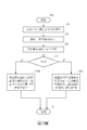
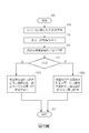
請參照第1圖,其係為本發明一實施例之應用於一快閃記憶體控制器之方法流程圖,該方法當接收到來自於一主機裝置所傳送的一修剪/擦除命令(trim/erase/unmap command)時能夠快速地產生複數個有效頁數目(valid page count, VPC)的資訊或內容;該快閃記憶體控制器例如是被耦接於該主機裝置及一快閃記憶體裝置(例如一電路晶片)之間。此外,該快閃記憶體控制器與該快閃記憶體裝置可以是被包括於一固態硬碟裝置內。該快閃記憶體控制器通常採用或使用一H2F對照表(host-to-flash table)及一有效頁數目對照表(VPC table),分別對於該快閃記憶體裝置中的每一區塊來記錄所使用的多個邏輯位址與一或多個有效頁的個數。當該快閃記憶體控制器接收到該修剪/擦除命令,該快閃記憶體控制器被安排用來對該快閃記憶體裝置執行一相對應的修剪/擦除操作(trim/erase/unmap operation),而該快閃記憶體控制器需要去更新H2F對照表的內容及有效頁數目對照表的內容,而本案的方法可令該快閃記憶體控制器快速地產生或更新有效頁數目對照表的內容,使得可盡可能地節省過多的計算,從而達到大幅的效能改進。Please refer to FIG. 1, which is a flowchart of a method applied to a flash memory controller according to an embodiment of the present invention. The method receives a trim/erase command (trim) transmitted from a host device. /erase/unmap command) can quickly generate information or content of multiple valid page counts (valid page count, VPC); the flash memory controller is, for example, coupled to the host device and a flash memory Between body devices (such as a circuit chip). In addition, the flash memory controller and the flash memory device may be included in a solid state drive device. The flash memory controller usually uses or uses a H2F table (host-to-flash table) and a table of effective pages (VPC table) for each block in the flash memory device To record the multiple logical addresses used and the number of one or more valid pages. When the flash memory controller receives the trim/erase command, the flash memory controller is arranged to perform a corresponding trim/erase operation on the flash memory device (trim/erase/ unmap operation), and the flash memory controller needs to update the content of the H2F comparison table and the content of the effective page number comparison table, and the method in this case can enable the flash memory controller to quickly generate or update the effective page The content of the number comparison table makes it possible to save as much calculation as possible, so as to achieve a substantial performance improvement.
假若在不妨礙本發明的實施並大致上達到相同結果的前提下,第1圖所示之流程圖的步驟不需依照所示之確切順序進行,該些步驟也不需連續進行,也就是說,其他步驟可穿插其中。詳細步驟如下:If the steps of the flowchart shown in FIG. 1 do not need to be performed in the exact order shown, without prejudice to the implementation of the present invention and substantially the same result, the steps need not be performed continuously, that is to say , Other steps can be interspersed. The detailed steps are as follows:
步驟105:開始;Step 105: Start;
步驟110:存取有效頁數目對照表的資訊;Step 110: Access the information of the effective page number comparison table;
步驟115:接收來自於該主機裝置之一修剪/擦除命令(trim/erase/unmap command);Step 115: Receive a trim/erase/unmap command from the host device;
步驟120:從該修剪/擦除命令,得到要被擦除之一儲存空間(例如要被擦除之一邏輯儲存空間);Step 120: Obtain a storage space to be erased (for example, a logical storage space to be erased) from the trim/erase command;
步驟125:比較該儲存空間之一空間大小與一臨界值TH,決定該空間大小是否大於該臨界值;如果該空間大小係大於該臨界值TH,則流程進行步驟130A,反之,流程進行步驟130B;Step 125: Compare a space size of the storage space with a critical value TH to determine whether the space size is greater than the critical value; if the space size is greater than the critical value TH, the process proceeds to step 130A, otherwise, the process proceeds to
步驟130A:重置該快閃記憶體裝置之複數個區塊的複數個有效頁數目的值為零,以及重建不被該修剪/擦除命令所擦除之一另一儲存空間的複數個有效頁數目的值;
步驟130B:根據要被擦除之該儲存空間之邏輯位址,逐次減少(decrement)至少一區塊之至少一有效頁數目的值;以及
步驟135:結束。Step 135: End.
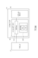
第2圖是根據第1圖所示之流程實施例之耦接於主機裝置201與快閃記憶體裝置202之間的一快閃記憶體控制器200的方塊示意圖。快閃記憶體裝置202例如是一快閃記憶體晶片,該晶片包含複數個區塊,每一區塊包含複數個儲存頁,例如,快閃記憶體裝置202可以是NAND快閃記憶體晶片(但並非限制)。此外,快閃記憶體控制器200與快閃記憶體裝置202可以被包括於一儲存裝置203內部,儲存裝置203例如是一固態硬碟裝置、一SD卡、一USB隨身碟或一嵌入式儲存裝置(但不限定)。快閃記憶體控制器200包含一儲存電路2005以及一處理電路2010,儲存電路2005例如是一隨機存取記憶體(但不限定)並被用來儲存有效頁數目對照表的資訊或內容,快閃記憶體裝置202具有複數個區塊(儲存區塊),而每一區塊具有複數個儲存頁,有效頁數目對照表的多個相對應的欄位或項目係被分別用來記錄快閃記憶體裝置202的所有區塊的複數個有效頁數目的值。FIG. 2 is a block diagram of a
實作上,在本實施例,儲存電路2005可被用來儲存有效頁數目對照表的資訊或內容以及儲存H2F對照表的資訊或內容,但這並不是本案的限制,在另一實施例,上述兩個對照表或上述的其中一個對照表均可被儲存於外部耦接於快閃記憶體控制器200的一另一不同的記憶體裝置。In practice, in this embodiment, the
處理電路2010在步驟110係被安排用來存取有效頁數目對照表的資訊,有效頁數目對照表記錄該複數個區塊的複數個有效頁數目的值,該複數個區塊例如是快閃記憶體裝置202的所有區塊,處理電路2010在步驟115係從主機裝置201(例如一電腦)接收該修剪/擦除命令,舉例來說,如果快閃記憶體控制器200支援一修剪/擦除命令的功能,主機裝置201可通過發送該修剪/擦除命令至快閃記憶體控制器200來要求快閃記憶體控制器200抹除一特別的儲存空間。The
實作上,快閃記憶體控制器200的處理電路2010被安排用來於每次當初始化一資料程式化(寫入)操作時,程式化(寫入)一儲存頁資料至快閃記憶體裝置202的一區塊的一儲存頁。此外,快閃記憶體控制器200的處理電路2010被安排用來於每次當初始化一資料抹除操作時抹除快閃記憶體裝置202的一區塊的所有儲存頁的內容,亦即,快閃記憶體控制器200係每次寫入或程式化一儲存頁,以及每次抹除一個區塊。In practice, the
快閃記憶體控制器200包括H2F對照表(或稱為邏輯位址-實體位址對照表(logical-to-physical (L2P) table),快閃記憶體控制器200的處理電路2010可依序地指派不同的邏輯位址給不同筆的儲存頁資料。而對於寫入一儲存頁資料,H2F對照表的一個項目(item)可被用來記錄哪一個實體區塊的哪一個實體儲存頁被用來儲存該儲存頁資料,實作上,該H2F對照表包含一定個數的項目,分別對應於快閃記憶體裝置202的所有實體區塊的所有實體儲存頁,當快閃記憶體控制器200寫入一儲存頁資料至一區塊的一儲存頁時,快閃記憶體控制器200的處理電路2010被安排用來將該儲存頁資料所使用的一邏輯位址記錄於該H2F對照表中與該區塊之該儲存頁有關的一相對應的項目,當寫入一不同儲存頁資料至一不同儲存頁時,快閃記憶體控制器200的處理電路2010被安排用來將該另一儲存頁資料所使用的一相對應邏輯位址記錄於該H2F對照表中與該另一儲存頁有關的一相對應的項目,如此,當後續存取快閃記憶體裝置202來獲取某一儲存頁資料時,快閃記憶體控制器200基於該某一儲存頁資料的邏輯位址來對H2F對照表進行查表,即可得知哪一個實體儲存區塊的哪一個實體儲存頁被用來儲存該儲存頁資料,並接著正確地取得或讀出該儲存頁資料。The
快閃記憶體控制器200包括該有效頁數目對照表,該有效頁數目對照表包含有一定個數的項目,其中每一項目係用來儲存一相對應區塊的一或多個有效頁的總數的值,基本上,在該有效頁數目對照表中的多個項目的個數係相同於在快閃記憶體裝置202中的區塊的個數,然而這並非是本案的限制。對於一特定區塊來說,當快閃記憶體控制器200寫入一儲存頁資料至該特定區塊之一空的儲存頁及記錄一特別的邏輯位址於該H2F對照表中與該空的儲存頁有關之一相對應的項目時,該特定區塊之一或多個有效頁的個數,亦即該特定區塊之一有效頁數目的值,係會被快閃記憶體控制器200的處理電路2010增加一。而如果該相同的邏輯位址在先前已經被其他儲存頁資料所使用,則當該邏輯位址已經記錄於該H2F對照表中與該不同區塊之一儲存頁有關之一項目,另一不同區塊的一有效頁數目的值係會被快閃記憶體控制器200的處理電路2010減少一。The
此外,快閃記憶體裝置202被設計包含有一使用者資料儲存區與一保留儲存區(例如一系統區與一保留區),該使用者資料儲存區係用來儲存使用者資料並經常或幾乎大於快閃記憶體裝置202之總儲存空間/容量的一半, 該保留儲存區係用來儲存重要檔案的資訊,例如系統檔案、操作系統開機程序等,例如,總儲存空間的百分之十可被用來作為該保留儲存區,而總儲存空間的其他部分可用來作為該使用者資料儲存區,然而,這並非是本發明的限制。In addition, the
主機裝置201可發送該修剪/擦除命令至快閃記憶體控制器200以抹除快閃記憶體裝置200中除了該保留儲存區以外的其他所有的區塊,例如,當如果快閃記憶體裝置202被第一次使用時或者已經變髒時(dirty)而決定去清除或抹除區塊的內容,主機裝置201可以發送修剪/擦除命令至快閃記憶體控制器200,應注意的是從一主機端接收該修剪/擦除命令的時間點並非是本發明的限制,快閃記憶體控制器200可在任何可能的情況下接收這樣的命令。The
實作上,當快閃記憶體控制器200接收該修剪/擦除命令且該修剪/擦除命令指示出抹除該使用者資料儲存區的區塊而非該保留儲存區時,快閃記憶體控制器200的處理電路2010被安排用來將快閃記憶體裝置202的所有區塊的所有有效頁數目的值均重置為零,也就是,快閃記憶體控制器200會將所有區塊(包含該保留儲存區的所有區塊)的所有有效頁數目的值均重置為零,接著,快閃記憶體控制器200的處理電路2010會重建該保留儲存區的所有區塊的有效頁數目,而由於該保留儲存區的空間較小於該使用者資料儲存區的空間,重建該保留儲存區的所有區塊的有效頁數目之值所需要花費的計算時間遠短於直接對該使用者資料儲存區的所有區塊的有效頁數目每次減一所需要花費的計算時間,如此,快閃記憶體控制器200可達到快速產生有效頁數目對照表的資訊/內容的效果。In practice, when the
舉例來說,執行重建一區塊的一有效頁數目之操作可通過一個儲存頁接著一個儲存頁的方式來計算及逐次累加(每次加一)該區塊之一或多個有效頁的個數來進行,而這樣的操作係不同於直接通過一個儲存頁接著一個儲存頁的方式來逐次減少(每次減一)一個區塊之一或多個有效頁的個數之操作,以下為了簡化描述這些操作,例如假設一快閃記憶體裝置包括了四個區塊BLK1、BLK2、BLK3及BLK4,每一個區塊具有四個儲存頁(總共十六個儲存頁),以及總共存在有十個邏輯位址LBA0至LBA9;然而,這並非是本案的限制。For example, the operation of rebuilding the number of valid pages of a block can be calculated and accumulated one by one (multiple by one) for one or more valid pages of the block by means of one storage page after another. This operation is different from the operation of directly reducing (one by one) the number of one or more valid pages in a block by directly storing one page after another. To simplify the description of these operations, for example, suppose a flash memory device includes four blocks BLK1, BLK2, BLK3, and BLK4, each block has four storage pages (a total of sixteen storage pages), and there are a total of ten Logical addresses LBA0 to LBA9; however, this is not a limitation of this case.
例如快閃記憶體控制器200可依序地使用該些邏輯位址LBA0至LBA9來寫入不同筆的資料單元(不同的儲存頁資料)至快閃記憶體裝置的區塊的儲存頁,例如,如果是十筆資料單元被依序地寫入至快閃記憶體裝置,則在以下H2F對照表中,處理電路2010會把對應於區塊BLK1的四個欄位上的項目記錄為LBA0、LBA1、LBA2及LBA3,並且將對應於區塊BLK2的四個欄位上的項目記錄為LBA4、LBA5、LBA6及LBA7,同樣地,處理電路2010會把對應於區塊BLK3的兩個欄位上的項目記錄為LBA8及LBA9,而剩下兩個欄位上的項目為空的,並且對應於區塊BLK4的四個欄位上的項目也是空的,因此,在有效頁數目對照表中,區塊BLK1、BLK2、BLK3及BLK4的四個有效頁數目分別會記錄為4、4、2、0;該H2F對照表及有效頁數目對照表的例子可顯示如下:

之後,處理電路2010寫入另一個資料單元至該快閃記憶體裝置,而在H2F對照表中處理電路2010被安排將對應於區塊BLK3之第三個欄位的項目記錄為LBA0,對應於區塊BLK1的第一個欄位之項目先前所記錄的LBA0變成是無效的,亦即一個無效儲存頁,快閃記憶體控制器200的處理電路2010會根據目前的有效頁,將區塊BLK1的有效頁數目的值減去一,並且將區塊BLK3的有效頁數目的值增加一,如此,在有效頁數目對照表中,區塊BLK1、BLK2、BLK3及BLK4的四個有效頁數目分別會記錄為3、4、3、0;該H2F對照表及有效頁數目對照表的例子可顯示如下:

於此情況下,如果主機裝置201 發送一修剪/擦除命令至快閃記憶體控制器200,並且該修剪/擦除命令係指示了要修剪(trim)或抹除(erase)具有邏輯位址從LBA1至LBA9之一儲存空間,則快閃記憶體控制器200的處理電路2010會被安排得到沒有要被該修剪/擦除命令修剪或抹除的另一不同儲存空間的一或多個邏輯位址,例如,如果該修剪/擦除命令被安排要抹除一使用者資料儲存區的一儲存空間,則沒有要被該修剪/擦除命令修剪或抹除的該另一不同儲存空間可以是一保留儲存區。而在這個例子中(修剪或抹除邏輯位址從LBA1至LBA9之儲存空間),快閃記憶體控制器200會得到沒有要被擦除的邏輯位址LBA0。In this case, if the
快閃記憶體控制器200的處理電路2010會清空/重置記錄於H2F對照表中該儲存空間從邏輯位址LBA1至LBA9的項目,並且也會清空或重置有效頁數目對照表中所有區塊的所有有效頁數目的值為零,接著快閃記憶體控制器200被安排用來根據所得到之沒有要被擦除之儲存空間的至少一邏輯位址,來計算並累加所有有效頁的個數來重建有效頁數目對照表中的一或多個有效頁數個的值。處理電路2010被安排用來以一個儲存頁接著一個儲存頁的方式逐次檢查是否對應於沒有要被擦除之儲存空間的儲存頁是有效頁或是無效儲存頁,等效上,處理電路2010會被安排逐次累加對應於沒有要被擦除之儲存空間的某些一或多個區塊的一或多個有效頁數目的值。舉例來說,在上述例子中,快閃記憶體控制器200只要在所有有效頁數目的值均被重置並零之後將區塊BLK3的有效頁數目的值加一(從零變為1),就可快速地重建有效頁數目對照表的正確資訊;該H2F對照表及有效頁數目對照表的例子可顯示如下:
重置有效頁數目對照表:


相較來說,由於傳統現有的機制需要依順序檢查對應於邏輯位址從LBA1至LBA9的九個儲存頁並按一個儲存頁接著一個儲存頁的方式來計算多個有效頁數目的值,所以,根據要被擦除的邏輯位址LBA1至LBA9,現有機制需要將相對應的多個區塊的多個有效頁數目的值逐次減一並執行九次,才能夠得到有效頁數目對照表的正確資訊。而在本發明的實施例,快閃記憶體控制器200通過先將所有的有效頁數目的值重置為零、接著再根據沒有要被擦除之儲存空間來計算一或多個有效頁數目的值並逐次累加,就可以快速地產生有效頁數目對照表的正確資訊。再者,應注意的是上述所提到之實施例中的對照表範例僅是用以解釋本發明的技術精神,而並非是本案的限制。In contrast, since the conventional existing mechanism needs to sequentially check the nine storage pages corresponding to the logical addresses from LBA1 to LBA9 and calculate the value of the number of effective pages in a way of one storage page after another storage page, so , According to the logical addresses LBA1 to LBA9 to be erased, the existing mechanism needs to reduce the value of the number of multiple valid pages of the corresponding multiple blocks one by one and execute them nine times in order to get the comparison table of the number of valid pages Correct information. In the embodiment of the present invention, the
此外,本案的操作係特別有用於當修剪/擦除命令係用來抹除大於一特別儲存空間(例如整個儲存空間)之一半的一儲存空間時,也就是特別有用於例如當要被抹除的儲存空間大於該快閃記憶體裝置之整個實體儲存空間的一半時,或是特別有用於當要被抹除的儲存空間大於使用者資料區的一半時;然此均並非是本案的限制。在另一實施例,快閃記憶體控制器200的處理電路2010會被安排用來決定要被一修剪/擦除命令所擦除之一儲存空間的大小是否大於一特定臨界值TH,特定臨界值TH例如是整個實體儲存空間的一半或是使用者資料區的一半。如果要被擦除之儲存空間的大小係大於特定臨界值TH,則處理電路2010 會被安排用來重置所有的有效頁數目的值,並接著根據沒有要被擦除之其他不同儲存空間來逐次累加一或多個有效頁數目的值,反之,如果要被擦除之儲存空間的大小係小於特定臨界值TH,則處理電路2010 會被安排用來直接根據要被擦除之儲存空間來對一或多個有效頁數目的值逐次減一,以產生有效頁數目對照表的資訊或內容。In addition, the operation in this case is particularly useful when the trim/erase command is used to erase a storage space larger than one-half of a special storage space (such as the entire storage space), which is particularly useful when, for example, it is to be erased When the storage space of the flash memory device is greater than half of the entire physical storage space of the flash memory device, or it is particularly useful when the storage space to be erased is greater than half of the user data area; however, this is not a limitation of this case. In another embodiment, the
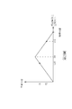
請參照第3圖,其所繪示為當分別接收到不同修剪/擦除命令以抹除具有不同空間大小之儲存空間時快閃記憶體控制器200的效能示意圖,如第3圖所示,水平軸表示要被擦除之儲存空間(或實體儲存空間)之不同空間大小,垂直軸表示當接收到修剪/擦除命令以抹除水平軸所定義之一儲存空間大小時完成計算有效頁數目對照表之內容的相對應等待時間。Please refer to FIG. 3, which is a schematic diagram illustrating the performance of the
舉例來說,在第一個例子中,處理電路2010從主機裝置201接收到一第一修剪/擦除命令,並接著被安排用來對快閃記憶體裝置202執行一第一修剪/擦除操作,快閃記憶體控制器200的處理電路2010從該第一修剪/擦除命令得到要被擦除之一第一儲存空間,在本例子中該第一儲存空間的大小LS1係小於特定臨界值TH(例如整個儲存空間的一半),快閃記憶體控制器200的處理電路2010係被安排用來清空在該H2F對照表中記錄有第一儲存空間的多個邏輯位址的多個項目,並直接對於該第一儲存空間所包括之多個邏輯位址所對應之多個有效頁數目的值進行逐次減一的運算,以產生或更新該有效頁數目對照表的資訊/內容,完成該第一修剪/擦除操作需要等待一時間T1。另外,在第二個例子中,快閃記憶體控制器200的處理電路2010從主機裝置201接收到一第二修剪/擦除命令,並接著被安排用來對快閃記憶體裝置202執行一第二修剪/擦除操作(trim/erase/unmap operation),快閃記憶體控制器200的處理電路2010從該第二修剪/擦除命令得到要被擦除之一第二儲存空間,在本例子中該第二儲存空間的大小LS2係大於特定臨界值TH(例如整個儲存空間的一半),快閃記憶體控制器200的處理電路2010係被安排用來清空在該H2F對照表中記錄有第二儲存空間的多個邏輯位址的多個項目、重置該有效頁數目對照表中所有區塊之所有的有效頁數目的值、以及通過對於不包括第二儲存空間的其他多個邏輯位址所對應之多個有效頁數目的值逐次進行加一的運算來重建對應於不包括第二儲存空間的該其他多個邏輯位址之有效頁數目的值,完成該第二修剪/擦除操作僅需要等待一時間T2,其較短於時間T1。For example, in the first example, the
相較於傳統的機制,如果傳統機制需要等待時間T1來完成對於要被擦除之儲存空間大小LS1的有效頁數目對照表的計算,則該傳統機制必然需要等待更長的時間來完成對於要被擦除之儲存空間大小LS2的有效頁數目對照表的計算,而對於傳統機制來說,這樣更長的等待時間通常是等同於時間T1再乘上一個T1除以T2的倍數。而在本發明實施例中,即使快閃記憶體控制器200在第二個例子中係被安排用來抹除一個具有較多邏輯位址之較大儲存空間LS2,然而,通過上述重置及重建的步驟,快閃記憶體控制器200可省去較多的資料計算,並且所花費的時間T2較短於時間T1。Compared with the traditional mechanism, if the traditional mechanism needs a waiting time T1 to complete the calculation of the effective page number comparison table of the storage space size LS1 to be erased, then the traditional mechanism must wait for a longer time to complete The calculation of the effective page number of the storage space size LS2 to be erased is compared with the calculation table. For the traditional mechanism, such a longer waiting time is usually equivalent to the time T1 multiplied by a multiple of T1 divided by T2. In the embodiment of the present invention, even though the
再者,在另一實施例,臨界值TH的值係為可調整的並且可以被使用者所決定。再者,第2圖的儲存電路2005可被設置為不包括於快閃記憶體控制器200內,而是外部連接至快閃記憶體控制器200,這樣的實施變型也可落入本發明的範疇。Furthermore, in another embodiment, the value of the threshold TH is adjustable and can be determined by the user. Furthermore, the
另外,在其他實施例,可假設從主機裝置201所發送的一修剪/擦除命令可以是預設用來抹除一個較大的邏輯/實體空間,其大小大於整個實體儲存空間的一半。一旦接收到該修剪/擦除命令,快閃記憶體控制器200的處理電路2010可對於該有效頁數目對照表執行上述的重置與重建步驟,也就是,處理電路2010可被用來決定一個要被擦除的儲存空間之大小是否大於臨界值TH;這樣的設計變型也符合本發明的精神。第4圖顯示了該設計變型實施例的流程圖,為簡化說明書的內容,其詳細說明不再贅述。In addition, in other embodiments, it can be assumed that a trim/erase command sent from the
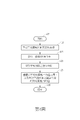
再者,在其他實施例,當接收到該修剪/擦除命令且該修剪/擦除命令指示出要被擦除之另一儲存空間時,處理電路2010可等效上得到沒有要被擦除之一儲存空間,例如,對於位址LBA0至LBA9所對應之空間而言,如果該修剪/擦除命令被安排用來抹除與位址LBA1至LBA9相關連的空間,則處理電路2010可得到一個相對應的沒有要被擦除的空間,亦即對應於位址LBA0的空間,當得到沒有要被擦除之該儲存空間時,處理電路2010被安排用來比較沒有要被擦除之該儲存空間的一空間大小與一臨界值(例如上述的臨界值TH),以決定該空間大小是否小於該臨界值,而接著當該空間大小係小於該臨界值時,重置快閃記憶體裝置202的複數個區塊之複數個有效頁數目的值。第5圖是本發明第三實施例之應用於一快閃記憶體控制器200之方法流程圖,該方法當接收到來自於主機裝置201所傳送的一修剪/擦除命令(trim/erase/unmap command)時能夠快速地產生複數個有效頁數目的資訊或內容。假若在不妨礙本發明的實施並大致上達到相同結果的前提下,第5圖所示之流程圖的步驟不需依照所示之確切順序進行,該些步驟也不需連續進行,也就是說,其他步驟可穿插其中。詳細步驟如下:Furthermore, in other embodiments, when the trim/erase command is received and the trim/erase command indicates another storage space to be erased, the
步驟505:開始;Step 505: Start;
步驟510:存取有效頁數目對照表的資訊;Step 510: Access the information of the effective page number comparison table;
步驟515:接收來自於該主機裝置之一修剪/擦除命令;Step 515: Receive a trim/erase command from the host device;
步驟520:從該修剪/擦除命令,得到沒有要被擦除之一儲存空間;Step 520: From the pruning/erasing command, obtain a storage space that is not to be erased;
步驟525:比較沒有要被擦除之該儲存空間之一空間大小與一臨界值TH,決定該空間大小是否小於該臨界值TH;如果該空間大小係小於該臨界值TH,則流程進行步驟530A,反之,流程進行步驟530B;Step 525: Compare a space size of the storage space that is not to be erased with a threshold value TH, and determine whether the space size is smaller than the threshold value TH; if the space size is smaller than the threshold value TH, the process proceeds to step 530A , Otherwise, the process proceeds to step 530B;
步驟530A:重置該快閃記憶體裝置之複數個區塊的複數個有效頁數目的值為零,以及重建不被該修剪/擦除命令所擦除之一另一儲存空間的複數個有效頁數目的值;
步驟530B:根據要被擦除之該儲存空間之邏輯位址,對至少一區塊之至少一有效頁數目的值逐次地減一;以及
步驟535:結束。 以上所述僅為本發明之較佳實施例,凡依本發明申請專利範圍所做之均等變化與修飾,皆應屬本發明之涵蓋範圍。 Step 535: End. The above are only the preferred embodiments of the present invention, and all changes and modifications made in accordance with the scope of the patent application of the present invention shall fall within the scope of the present invention.

第1圖為本發明一實施例之應用於一快閃記憶體控制器之方法流程圖。 第2圖是根據第1圖所示之流程實施例之耦接於主機裝置與快閃記憶體裝置之間的一快閃記憶體控制器的方塊示意圖。 第3圖為當分別接收到不同修剪/擦除命令以抹除具有不同空間大小之儲存空間時快閃記憶體控制器的效能示意圖。 第4圖為本發明第二實施例之應用於快閃記憶體控制器之方法流程圖。 第5圖為本發明第三實施例之應用於快閃記憶體控制器之方法流程圖。 FIG. 1 is a flowchart of a method applied to a flash memory controller according to an embodiment of the invention. FIG. 2 is a block diagram of a flash memory controller coupled between the host device and the flash memory device according to the process embodiment shown in FIG. 1. FIG. FIG. 3 is a schematic diagram of the performance of the flash memory controller when different pruning/erasing commands are received to erase storage spaces having different space sizes. FIG. 4 is a flowchart of a method applied to a flash memory controller according to a second embodiment of the invention. FIG. 5 is a flowchart of a method applied to a flash memory controller according to a third embodiment of the invention.
Claims (25)
Applications Claiming Priority (2)
| Application Number | Priority Date | Filing Date | Title |
|---|---|---|---|
| US16/036,954 | 2018-07-17 | ||
| US16/036,954 US10936199B2 (en) | 2018-07-17 | 2018-07-17 | Flash controllers, methods, and corresponding storage devices capable of rapidly/fast generating or updating contents of valid page count table |
Publications (2)
| Publication Number | Publication Date |
|---|---|
| TW202006552A TW202006552A (en) | 2020-02-01 |
| TWI690803B true TWI690803B (en) | 2020-04-11 |
Family
ID=69162418
Family Applications (2)
| Application Number | Title | Priority Date | Filing Date |
|---|---|---|---|
| TW108104772A TWI690803B (en) | 2018-07-17 | 2019-02-13 | Flash controllers, methods, and corresponding storage devices capable of rapidly/fast generating or updating contents of valid page count table |
| TW109107258A TWI759699B (en) | 2018-07-17 | 2019-02-13 | Flash controllers, methods, and corresponding storage devices capable of rapidly/fast generating or updating contents of valid page count table |
Family Applications After (1)
| Application Number | Title | Priority Date | Filing Date |
|---|---|---|---|
| TW109107258A TWI759699B (en) | 2018-07-17 | 2019-02-13 | Flash controllers, methods, and corresponding storage devices capable of rapidly/fast generating or updating contents of valid page count table |
Country Status (3)
| Country | Link |
|---|---|
| US (2) | US10936199B2 (en) |
| CN (1) | CN110727395B (en) |
| TW (2) | TWI690803B (en) |
Families Citing this family (9)
| Publication number | Priority date | Publication date | Assignee | Title |
|---|---|---|---|---|
| KR20200033625A (en) * | 2018-09-20 | 2020-03-30 | 에스케이하이닉스 주식회사 | Apparatus and method for checking valid data in memory system |
| JP2020135134A (en) * | 2019-02-14 | 2020-08-31 | 株式会社日立製作所 | Storage system and compaction method |
| CN111625187B (en) * | 2020-05-15 | 2023-09-29 | 合肥康芯威存储技术有限公司 | Memory, control method thereof and memory system |
| US20220222008A1 (en) * | 2021-01-14 | 2022-07-14 | Silicon Motion, Inc. | Method for managing flash memory module and associated flash memory controller and memory device |
| US11733895B2 (en) | 2021-03-31 | 2023-08-22 | Silicon Motion, Inc. | Control method of flash memory controller and associated flash memory controller and storage device |
| US11748011B2 (en) * | 2021-03-31 | 2023-09-05 | Silicon Motion, Inc. | Control method of flash memory controller and associated flash memory controller and storage device |
| US20230043338A1 (en) * | 2021-08-06 | 2023-02-09 | Micron Technology, Inc. | Techniques for memory zone size adjustment |
| CN116931812A (en) * | 2022-03-31 | 2023-10-24 | 慧荣科技股份有限公司 | Data access method and storage medium and apparatus for responding to host discard command |
| CN116880777B (en) * | 2023-09-07 | 2023-12-01 | 合肥康芯威存储技术有限公司 | Embedded memory and flash memory recovery method |
Citations (6)
| Publication number | Priority date | Publication date | Assignee | Title |
|---|---|---|---|---|
| TW200905680A (en) * | 2007-06-08 | 2009-02-01 | Sandisk Corp | Method and system for storage address re-mapping for a memory device |
| TW201142589A (en) * | 2010-05-24 | 2011-12-01 | Silicon Motion Inc | Apparatuses for managing and accessing flash memory module |
| TW201305818A (en) * | 2011-07-21 | 2013-02-01 | Phison Electronics Corp | Data writing method, memory controller and memory storage apparatus |
| TW201312353A (en) * | 2011-09-06 | 2013-03-16 | Phison Electronics Corp | Data moving mehod, memory controller and memory storage apparatus |
| TW201616363A (en) * | 2014-10-31 | 2016-05-01 | 慧榮科技股份有限公司 | Data storage device and flash memory control method |
| TW201626233A (en) * | 2014-11-25 | 2016-07-16 | 旺宏電子股份有限公司 | Variant operation sequences for multibit memory |
Family Cites Families (55)
| Publication number | Priority date | Publication date | Assignee | Title |
|---|---|---|---|---|
| JP2763080B2 (en) * | 1992-03-18 | 1998-06-11 | 富士通株式会社 | Optical disk drive |
| US5361228A (en) * | 1992-04-30 | 1994-11-01 | Fuji Photo Film Co., Ltd. | IC memory card system having a common data and address bus |
| US5682499A (en) * | 1995-06-06 | 1997-10-28 | International Business Machines Corporation | Directory rebuild method and apparatus for maintaining and rebuilding directory information for compressed data on direct access storage device (DASD) |
| US6175906B1 (en) * | 1996-12-06 | 2001-01-16 | Advanced Micro Devices, Inc. | Mechanism for fast revalidation of virtual tags |
| US7984303B1 (en) * | 2000-01-06 | 2011-07-19 | Super Talent Electronics, Inc. | Flash memory devices with security features |
| US6839873B1 (en) * | 2000-06-23 | 2005-01-04 | Cypress Semiconductor Corporation | Method and apparatus for programmable logic device (PLD) built-in-self-test (BIST) |
| US7322029B2 (en) * | 2003-05-08 | 2008-01-22 | American Megatrends, Inc. | Method and system for recovering program code in a computer system |
| US7012835B2 (en) * | 2003-10-03 | 2006-03-14 | Sandisk Corporation | Flash memory data correction and scrub techniques |
| US7173852B2 (en) * | 2003-10-03 | 2007-02-06 | Sandisk Corporation | Corrected data storage and handling methods |
| KR101087906B1 (en) * | 2003-11-18 | 2011-11-30 | 파나소닉 주식회사 | File recording device |
| JP2006039966A (en) * | 2004-07-27 | 2006-02-09 | Toshiba Corp | Memory card, card controller installed in memory card, and processing unit of memory card |
| JP4192129B2 (en) * | 2004-09-13 | 2008-12-03 | 株式会社東芝 | Memory management device |
| JP4956922B2 (en) * | 2004-10-27 | 2012-06-20 | ソニー株式会社 | Storage device |
| KR100626391B1 (en) * | 2005-04-01 | 2006-09-20 | 삼성전자주식회사 | Onenand flash memory and data processing system including the same |
| US9286198B2 (en) * | 2005-04-21 | 2016-03-15 | Violin Memory | Method and system for storage of data in non-volatile media |
| KR100708128B1 (en) * | 2005-04-30 | 2007-04-17 | 삼성전자주식회사 | An apparatus and method for controlling nand flash memory |
| US20070083697A1 (en) * | 2005-10-07 | 2007-04-12 | Microsoft Corporation | Flash memory management |
| JP5145720B2 (en) * | 2007-01-31 | 2013-02-20 | 富士通セミコンダクター株式会社 | Charge loss repair method and semiconductor memory device |
| KR100869675B1 (en) * | 2007-02-05 | 2008-11-21 | 지인정보기술 주식회사 | System and method for controling flash memory using descriptor array |
| US8397011B2 (en) * | 2007-10-05 | 2013-03-12 | Joseph Ashwood | Scalable mass data storage device |
| JP5143601B2 (en) * | 2008-03-24 | 2013-02-13 | 株式会社日立製作所 | Information processing apparatus, information processing method, and storage system |
| US20090271562A1 (en) * | 2008-04-25 | 2009-10-29 | Sinclair Alan W | Method and system for storage address re-mapping for a multi-bank memory device |
| CN101571832B (en) * | 2008-04-29 | 2013-07-17 | 群联电子股份有限公司 | Data writing method, quick flashing memory system using same and a controller thereof |
| US8285970B2 (en) * | 2008-11-06 | 2012-10-09 | Silicon Motion Inc. | Method for managing a memory apparatus, and associated memory apparatus thereof |
| US8612718B2 (en) * | 2009-08-19 | 2013-12-17 | Seagate Technology Llc | Mapping alignment |
| US9223514B2 (en) * | 2009-09-09 | 2015-12-29 | SanDisk Technologies, Inc. | Erase suspend/resume for memory |
| US8327092B2 (en) * | 2009-09-21 | 2012-12-04 | Freescale Semiconductor, Inc. | Memory device configurable as interleaved or non-interleaved memory |
| US20110161560A1 (en) * | 2009-12-31 | 2011-06-30 | Hutchison Neil D | Erase command caching to improve erase performance on flash memory |
| US9134918B2 (en) * | 2009-12-31 | 2015-09-15 | Sandisk Technologies Inc. | Physical compression of data with flat or systematic pattern |
| JP5066209B2 (en) * | 2010-03-18 | 2012-11-07 | 株式会社東芝 | Controller, data storage device, and program |
| US8812816B2 (en) * | 2010-03-23 | 2014-08-19 | Apple Inc. | Garbage collection schemes for index block |
| US8843731B2 (en) * | 2010-12-30 | 2014-09-23 | Micron Technology, Inc. | Memory device using extended interface commands |
| KR101392174B1 (en) * | 2011-11-09 | 2014-05-09 | 한양대학교 산학협력단 | Apparatus and method for controlling flash memory storing mapping table of block to erase |
| US9164887B2 (en) * | 2011-12-05 | 2015-10-20 | Industrial Technology Research Institute | Power-failure recovery device and method for flash memory |
| US9116792B2 (en) * | 2012-05-18 | 2015-08-25 | Silicon Motion, Inc. | Data storage device and method for flash block management |
| US8799561B2 (en) * | 2012-07-27 | 2014-08-05 | International Business Machines Corporation | Valid page threshold based garbage collection for solid state drive |
| KR20140026758A (en) * | 2012-08-23 | 2014-03-06 | 에스케이하이닉스 주식회사 | Nonvolatile memory device and nonvolatile memory system including the same |
| US9336090B2 (en) * | 2012-10-10 | 2016-05-10 | Hitachi, Ltd. | Storage apparatus comprising snapshot function, and storage control method |
| FR3006804A1 (en) * | 2013-06-05 | 2014-12-12 | St Microelectronics Rousset | BLOCK ERASING PROCESS OF A MEMORY OF ERASABLE EEPROM TYPE PER PAGE |
| US9298608B2 (en) * | 2013-10-18 | 2016-03-29 | Sandisk Enterprise Ip Llc | Biasing for wear leveling in storage systems |
| KR20150075886A (en) * | 2013-12-26 | 2015-07-06 | 에스케이하이닉스 주식회사 | Memory system and operating method thereof |
| US9423970B2 (en) * | 2013-12-30 | 2016-08-23 | Sandisk Technologies Llc | Method and system for predicting block failure in a non-volatile memory |
| US9329797B2 (en) * | 2013-12-30 | 2016-05-03 | Sandisk Technologies Inc. | Method and system for adjusting block erase or program parameters based on a predicted erase life |
| US20160232088A1 (en) * | 2014-07-17 | 2016-08-11 | Sandisk Enterprise Ip Llc | Garbage Collection in Storage System with Distributed Processors |
| US9490017B2 (en) * | 2015-03-10 | 2016-11-08 | Macronix International Co., Ltd. | Forced-bias method in sub-block erase |
| KR102371916B1 (en) * | 2015-07-22 | 2022-03-07 | 삼성전자주식회사 | Storage device for supporting virtual machines, storage system including the storage device, and method of the same |
| KR20180039785A (en) * | 2016-10-10 | 2018-04-19 | 에스케이하이닉스 주식회사 | Memory system and operation method for the same |
| IT201700020134A1 (en) * | 2017-02-22 | 2018-08-22 | St Microelectronics Srl | PROCEDURE FOR MANAGING SEMICONDUCTOR MEMORIES, INTERFACE, MEMORY AND CORRESPONDENT DEVICE |
| US20180285562A1 (en) * | 2017-03-31 | 2018-10-04 | Intel Corporation | Computing system with protection against memory wear out attacks |
| KR102233400B1 (en) * | 2017-05-29 | 2021-03-26 | 에스케이하이닉스 주식회사 | Data storage device and operating method thereof |
| KR20190012012A (en) * | 2017-07-26 | 2019-02-08 | 에스케이하이닉스 주식회사 | Memory device and operating method thereof |
| US20190035445A1 (en) * | 2017-07-31 | 2019-01-31 | CNEX Labs, Inc. a Delaware Corporation | Method and Apparatus for Providing Low Latency Solid State Memory Access |
| TWI633428B (en) * | 2017-09-28 | 2018-08-21 | 慧榮科技股份有限公司 | Data storage device and methods for processing data in the data storage device |
| KR102578191B1 (en) * | 2018-04-09 | 2023-09-14 | 에스케이하이닉스 주식회사 | Data Storage Device and Operation Method Optimized for Recovery Performance, Storage System Having the Same |
| US11100011B2 (en) * | 2018-12-13 | 2021-08-24 | Sony Semiconductor Israel Ltd. | Flash translation layer with hierarchical security |
-
2018
- 2018-07-17 US US16/036,954 patent/US10936199B2/en active Active
-
2019
- 2019-02-13 TW TW108104772A patent/TWI690803B/en active
- 2019-02-13 TW TW109107258A patent/TWI759699B/en active
- 2019-03-15 CN CN201910197688.XA patent/CN110727395B/en active Active
-
2021
- 2021-01-20 US US17/152,812 patent/US11630580B2/en active Active
Patent Citations (6)
| Publication number | Priority date | Publication date | Assignee | Title |
|---|---|---|---|---|
| TW200905680A (en) * | 2007-06-08 | 2009-02-01 | Sandisk Corp | Method and system for storage address re-mapping for a memory device |
| TW201142589A (en) * | 2010-05-24 | 2011-12-01 | Silicon Motion Inc | Apparatuses for managing and accessing flash memory module |
| TW201305818A (en) * | 2011-07-21 | 2013-02-01 | Phison Electronics Corp | Data writing method, memory controller and memory storage apparatus |
| TW201312353A (en) * | 2011-09-06 | 2013-03-16 | Phison Electronics Corp | Data moving mehod, memory controller and memory storage apparatus |
| TW201616363A (en) * | 2014-10-31 | 2016-05-01 | 慧榮科技股份有限公司 | Data storage device and flash memory control method |
| TW201626233A (en) * | 2014-11-25 | 2016-07-16 | 旺宏電子股份有限公司 | Variant operation sequences for multibit memory |
Also Published As
| Publication number | Publication date |
|---|---|
| TW202006552A (en) | 2020-02-01 |
| US10936199B2 (en) | 2021-03-02 |
| US20200026436A1 (en) | 2020-01-23 |
| TW202026887A (en) | 2020-07-16 |
| TWI759699B (en) | 2022-04-01 |
| CN110727395A (en) | 2020-01-24 |
| CN110727395B (en) | 2023-08-08 |
| US20210141537A1 (en) | 2021-05-13 |
| US11630580B2 (en) | 2023-04-18 |
Similar Documents
| Publication | Publication Date | Title |
|---|---|---|
| TWI690803B (en) | Flash controllers, methods, and corresponding storage devices capable of rapidly/fast generating or updating contents of valid page count table | |
| US9229876B2 (en) | Method and system for dynamic compression of address tables in a memory | |
| US10698809B2 (en) | Method, associated flash controller and electronic device for accessing flash module with data validity verification | |
| US8438361B2 (en) | Logical block storage in a storage device | |
| US11630766B2 (en) | Memory system and operating method thereof | |
| US11620066B2 (en) | Storage device with expandible logical address space and operating method thereof | |
| CN109697027B (en) | Data storage device including shared memory region and dedicated memory region | |
| US20180129602A1 (en) | Garbage collection method for data storage device | |
| US10073771B2 (en) | Data storage method and system thereof | |
| US11157399B2 (en) | Data storage devices and data processing methods with dynamic programming scheme | |
| US20170147232A1 (en) | Solid state drive and data programming method thereof | |
| TW201523253A (en) | Data storage device and data accessing method | |
| US11204864B2 (en) | Data storage devices and data processing methods for improving the accessing performance of the data storage devices | |
| US10606744B2 (en) | Method for accessing flash memory module and associated flash memory controller and electronic device | |
| US20240143219A1 (en) | Software-hardware combination method for internal mapping address query of zoned namespace | |
| US8429339B2 (en) | Storage device utilizing free pages in compressed blocks | |
| US9037781B2 (en) | Method for managing buffer memory, memory controllor, and memory storage device | |
| TWI584117B (en) | Data storage device and data fetching method for flash memory | |
| US20140089566A1 (en) | Data storing method, and memory controller and memory storage apparatus using the same | |
| KR102330394B1 (en) | Method for operating controller and method for operating device including the same | |
| US9652378B2 (en) | Writing method, memory controller and memory storage device | |
| US12061792B1 (en) | Method of handling host write commands requesting to write dummy pattern on flash memory and related memory controller and storage system | |
| US11704238B1 (en) | Method and apparatus for accessing L2P address without searching group-to-flash mapping table | |
| US11977767B2 (en) | Method and apparatus for caching address mapping information in flash memory based storage device | |
| US20240264757A1 (en) | Memory system and operating method thereof |