TW202248564A - Backlight module and electronic device including the same - Google Patents
Backlight module and electronic device including the same Download PDFInfo
- Publication number
- TW202248564A TW202248564A TW111121629A TW111121629A TW202248564A TW 202248564 A TW202248564 A TW 202248564A TW 111121629 A TW111121629 A TW 111121629A TW 111121629 A TW111121629 A TW 111121629A TW 202248564 A TW202248564 A TW 202248564A
- Authority
- TW
- Taiwan
- Prior art keywords
- reflective element
- light
- reflectivity
- circuit board
- backlight module
- Prior art date
Links
Images


Classifications
-
- G—PHYSICS
- G02—OPTICS
- G02B—OPTICAL ELEMENTS, SYSTEMS OR APPARATUS
- G02B6/00—Light guides; Structural details of arrangements comprising light guides and other optical elements, e.g. couplings
- G02B6/0001—Light guides; Structural details of arrangements comprising light guides and other optical elements, e.g. couplings specially adapted for lighting devices or systems
- G02B6/0011—Light guides; Structural details of arrangements comprising light guides and other optical elements, e.g. couplings specially adapted for lighting devices or systems the light guides being planar or of plate-like form
- G02B6/0033—Means for improving the coupling-out of light from the light guide
- G02B6/005—Means for improving the coupling-out of light from the light guide provided by one optical element, or plurality thereof, placed on the light output side of the light guide
- G02B6/0055—Reflecting element, sheet or layer
-
- G—PHYSICS
- G02—OPTICS
- G02F—OPTICAL DEVICES OR ARRANGEMENTS FOR THE CONTROL OF LIGHT BY MODIFICATION OF THE OPTICAL PROPERTIES OF THE MEDIA OF THE ELEMENTS INVOLVED THEREIN; NON-LINEAR OPTICS; FREQUENCY-CHANGING OF LIGHT; OPTICAL LOGIC ELEMENTS; OPTICAL ANALOGUE/DIGITAL CONVERTERS
- G02F1/00—Devices or arrangements for the control of the intensity, colour, phase, polarisation or direction of light arriving from an independent light source, e.g. switching, gating or modulating; Non-linear optics
- G02F1/01—Devices or arrangements for the control of the intensity, colour, phase, polarisation or direction of light arriving from an independent light source, e.g. switching, gating or modulating; Non-linear optics for the control of the intensity, phase, polarisation or colour
- G02F1/13—Devices or arrangements for the control of the intensity, colour, phase, polarisation or direction of light arriving from an independent light source, e.g. switching, gating or modulating; Non-linear optics for the control of the intensity, phase, polarisation or colour based on liquid crystals, e.g. single liquid crystal display cells
- G02F1/133—Constructional arrangements; Operation of liquid crystal cells; Circuit arrangements
- G02F1/1333—Constructional arrangements; Manufacturing methods
- G02F1/1335—Structural association of cells with optical devices, e.g. polarisers or reflectors
- G02F1/1336—Illuminating devices
- G02F1/133602—Direct backlight
- G02F1/133603—Direct backlight with LEDs
-
- G—PHYSICS
- G02—OPTICS
- G02B—OPTICAL ELEMENTS, SYSTEMS OR APPARATUS
- G02B6/00—Light guides; Structural details of arrangements comprising light guides and other optical elements, e.g. couplings
- G02B6/0001—Light guides; Structural details of arrangements comprising light guides and other optical elements, e.g. couplings specially adapted for lighting devices or systems
- G02B6/0011—Light guides; Structural details of arrangements comprising light guides and other optical elements, e.g. couplings specially adapted for lighting devices or systems the light guides being planar or of plate-like form
- G02B6/0013—Means for improving the coupling-in of light from the light source into the light guide
- G02B6/0023—Means for improving the coupling-in of light from the light source into the light guide provided by one optical element, or plurality thereof, placed between the light guide and the light source, or around the light source
- G02B6/0031—Reflecting element, sheet or layer
-
- G—PHYSICS
- G02—OPTICS
- G02B—OPTICAL ELEMENTS, SYSTEMS OR APPARATUS
- G02B6/00—Light guides; Structural details of arrangements comprising light guides and other optical elements, e.g. couplings
- G02B6/0001—Light guides; Structural details of arrangements comprising light guides and other optical elements, e.g. couplings specially adapted for lighting devices or systems
- G02B6/0011—Light guides; Structural details of arrangements comprising light guides and other optical elements, e.g. couplings specially adapted for lighting devices or systems the light guides being planar or of plate-like form
- G02B6/0075—Arrangements of multiple light guides
- G02B6/0078—Side-by-side arrangements, e.g. for large area displays
-
- G—PHYSICS
- G02—OPTICS
- G02F—OPTICAL DEVICES OR ARRANGEMENTS FOR THE CONTROL OF LIGHT BY MODIFICATION OF THE OPTICAL PROPERTIES OF THE MEDIA OF THE ELEMENTS INVOLVED THEREIN; NON-LINEAR OPTICS; FREQUENCY-CHANGING OF LIGHT; OPTICAL LOGIC ELEMENTS; OPTICAL ANALOGUE/DIGITAL CONVERTERS
- G02F1/00—Devices or arrangements for the control of the intensity, colour, phase, polarisation or direction of light arriving from an independent light source, e.g. switching, gating or modulating; Non-linear optics
- G02F1/01—Devices or arrangements for the control of the intensity, colour, phase, polarisation or direction of light arriving from an independent light source, e.g. switching, gating or modulating; Non-linear optics for the control of the intensity, phase, polarisation or colour
- G02F1/13—Devices or arrangements for the control of the intensity, colour, phase, polarisation or direction of light arriving from an independent light source, e.g. switching, gating or modulating; Non-linear optics for the control of the intensity, phase, polarisation or colour based on liquid crystals, e.g. single liquid crystal display cells
- G02F1/133—Constructional arrangements; Operation of liquid crystal cells; Circuit arrangements
- G02F1/1333—Constructional arrangements; Manufacturing methods
- G02F1/1335—Structural association of cells with optical devices, e.g. polarisers or reflectors
- G02F1/1336—Illuminating devices
- G02F1/133602—Direct backlight
- G02F1/133605—Direct backlight including specially adapted reflectors
Landscapes
- Physics & Mathematics (AREA)
- General Physics & Mathematics (AREA)
- Optics & Photonics (AREA)
- Nonlinear Science (AREA)
- Mathematical Physics (AREA)
- Chemical & Material Sciences (AREA)
- Crystallography & Structural Chemistry (AREA)
- Planar Illumination Modules (AREA)
- Devices For Indicating Variable Information By Combining Individual Elements (AREA)
Abstract
Description
本揭露係有關於電子裝置,且特別係有關於電子裝置的背光模組。The present disclosure relates to electronic devices, and particularly to backlight modules of electronic devices.
包含面板在內的電子產品,如顯示器、智慧型手機、平板電腦、筆記型電腦及電視,已成為現代社會不可或缺的必需品。隨著這類電子產品的蓬勃發展,消費者對這些產品的品質、功能或價格抱有很高的期望。Electronic products including panels, such as monitors, smartphones, tablets, laptops and televisions, have become an indispensable necessity in modern society. With the boom in such electronic products, consumers have high expectations for the quality, function or price of these products.
然而,這些電子產品並未在各個方面皆滿足消費者的期望,電子產品仍存在一些問題。例如,於具有背光模組的電子裝置中,鄰近發光元件設置的膠帶可能會影響背光模組的光提取效率(extraction efficiency)。開發可改善光提取效率之背光模組的結構設計仍為目前業界的目標之一。However, these electronic products do not meet consumers' expectations in every aspect, and there are still some problems in the electronic products. For example, in an electronic device with a backlight module, the adhesive tape disposed adjacent to the light-emitting element may affect the light extraction efficiency of the backlight module. Developing the structural design of the backlight module that can improve the light extraction efficiency is still one of the goals of the current industry.
根據本揭露一些實施例,提供一種背光模組,背光模組包含電路板、複數個發光元件、導光板、第一反射元件以及第二反射元件,電路板具有複數個光反射區域,複數個發光元件沿第一方向排列於電路板上,且朝向複數個光反射區域發光,導光板設置於電路板上,第一反射元件設置於導光板與電路板之間,且圍繞複數個發光元件,第二反射元件設置於導光板與電路板之間,且對應於複數個光反射區域。並且,第一反射元件具有第一反射率R1,第二反射元件具有第二反射率R2,且第一反射率R1以及第二反射率R2滿足下列公式:0 ≤ │(R1-R2)│/Max (R1, R2) < 20%。本揭露亦提供一種包含前述背光模組的電子裝置。According to some embodiments of the present disclosure, a backlight module is provided. The backlight module includes a circuit board, a plurality of light-emitting elements, a light guide plate, a first reflective element, and a second reflective element. The circuit board has a plurality of light-reflecting regions, and a plurality of light-emitting The elements are arranged on the circuit board along the first direction, and emit light toward a plurality of light reflection areas, the light guide plate is arranged on the circuit board, the first reflective element is arranged between the light guide plate and the circuit board, and surrounds the plurality of light emitting elements, the second The two reflection elements are disposed between the light guide plate and the circuit board, and correspond to a plurality of light reflection areas. Moreover, the first reflective element has a first reflectivity R1, the second reflective element has a second reflectivity R2, and the first reflectivity R1 and the second reflectivity R2 satisfy the following formula: 0 ≤ │(R1-R2)│/ Max (R1, R2) < 20%. The present disclosure also provides an electronic device including the aforementioned backlight module.
根據本揭露一些實施例,提供一種電子裝置,電子裝置包含顯示面板以及背光模組,背光模組設置於顯示面板下方,背光模組包含電路板、複數個發光元件、導光板、第一反射元件以及第二反射元件,電路板具有複數個光反射區域,複數個發光元件沿第一方向排列於電路板上,且朝向複數個光反射區域發光,導光板設置於電路板上,第一反射元件設置於導光板與電路板之間,且圍繞複數個發光元件,第二反射元件設置於導光板與電路板之間,且對應於複數個光反射區域。並且,第一反射元件具有第一反射率R1,第二反射元件具有第二反射率R2,且第一反射率R1以及第二反射率R2滿足下列公式:0 ≤ │(R1-R2)│/Max (R1, R2) < 20%。本揭露亦提供一種包含前述背光模組的電子裝置。According to some embodiments of the present disclosure, an electronic device is provided, the electronic device includes a display panel and a backlight module, the backlight module is disposed under the display panel, and the backlight module includes a circuit board, a plurality of light emitting elements, a light guide plate, and a first reflective element As well as the second reflective element, the circuit board has a plurality of light reflection areas, the plurality of light emitting elements are arranged on the circuit board along the first direction, and emit light toward the plurality of light reflection areas, the light guide plate is arranged on the circuit board, and the first reflective element It is arranged between the light guide plate and the circuit board and surrounds the plurality of light-emitting elements. The second reflection element is arranged between the light guide plate and the circuit board and corresponds to the plurality of light reflection areas. Moreover, the first reflective element has a first reflectivity R1, the second reflective element has a second reflectivity R2, and the first reflectivity R1 and the second reflectivity R2 satisfy the following formula: 0 ≤ │(R1-R2)│/ Max (R1, R2) < 20%. The present disclosure also provides an electronic device including the aforementioned backlight module.
為讓本揭露之特徵或優點能更明顯易懂,下文特舉出一些實施例,並配合所附圖式,作詳細說明如下。In order to make the features or advantages of the present disclosure more comprehensible, some embodiments are specifically cited below, together with the accompanying drawings, for detailed description as follows.
以下針對本揭露實施例的背光模組以及電子裝置作詳細說明。應了解的是,以下之敘述提供許多不同的實施例,用以實施本揭露一些實施例之不同態樣。以下所述特定的元件及排列方式僅為簡單清楚描述本揭露一些實施例。當然,這些僅用以舉例而非本揭露之限定。此外,在不同實施例中可能使用類似及/或對應的標號標示類似及/或對應的元件,以清楚描述本揭露。然而,這些類似及/或對應的標號的使用僅為了簡單清楚地敘述本揭露一些實施例,不代表所討論之不同實施例及/或結構之間具有任何關連性。The backlight module and the electronic device of the embodiments of the present disclosure will be described in detail below. It should be understood that the following description provides many different embodiments for implementing different aspects of some embodiments of the present disclosure. The specific components and arrangements described below are only for simple and clear description of some embodiments of the present disclosure. Of course, these are only examples rather than limitations of the present disclosure. In addition, similar and/or corresponding reference numerals may be used in different embodiments to denote similar and/or corresponding elements to clearly describe the present disclosure. However, the use of these similar and/or corresponding symbols is only for simply and clearly describing some embodiments of the present disclosure, and does not mean that there is any relationship between the different embodiments and/or structures discussed.
透過參考以下的詳細描述並同時結合圖式可以理解本揭露,應注意的是,為了使讀者能夠容易理解圖式,本揭露中的多張圖式只繪出電子裝置的一部分,且圖式中的特定元件並非依照實際比例繪製。此外,圖式中各元件的數量及尺寸僅作為示意,並非用來限制本揭露的範圍。The present disclosure can be understood by referring to the following detailed descriptions in combination with the drawings. It should be noted that, in order to make the drawings easier for readers to understand, the drawings in the present disclosure only depict a part of the electronic device, and in the drawings Certain elements are not drawn to actual scale. In addition, the quantity and size of each element in the drawings are only for illustration, and are not intended to limit the scope of the present disclosure.
本揭露通篇說明書以及後附的發明申請專利範圍中會使用某些詞彙來指稱特定元件。本發明所屬技術領域人員應理解,電子設備製造商可能會以不同的名稱來指稱相同的元件。本文並不意在區分那些功能相同但名稱不同的元件。在下文說明書與發明申請專利範圍中,「包括」、「包含」、「具有」等詞為開放式詞語,因此其應被解釋為「包含但不限定為…」之意。因此,當本揭露的描述中使用術語「包括」、「包含」及/或「具有」時,其指定了相應的特徵、區域、步驟、操作及/或構件的存在,但不排除一個或多個相應的特徵、區域、步驟、操作及/或構件的存在。Certain terms are used throughout this disclosure and in the appended claims to refer to specific elements. Those skilled in the art of the present invention should understand that manufacturers of electronic equipment may refer to the same component by different names. This document does not intend to distinguish between those elements that have the same function but have different names. In the description below and the scope of patent application for the invention, words such as "including", "comprising", and "having" are open-ended words, so they should be interpreted as meaning "including but not limited to...". Therefore, when the terms "comprising", "comprising" and/or "having" are used in the description of the present disclosure, it specifies the existence of corresponding features, regions, steps, operations and/or components, but does not exclude one or more The existence of a corresponding feature, region, step, operation and/or component.
本揭露中所提到的方向用語,例如「上」、「下」、「前」、「後」、「左」、「右」等,僅是參考圖式的方向。因此,使用的方向用語是作為示意,而並非用來限制本揭露。各圖式繪示的是特定實施例中所使用的方法、結構及/或材料的通常性特徵。然而,這些圖式不應被解釋為界定或限制由這些實施例所涵蓋的範圍或性質。舉例而言,為了清楚起見,各膜層、區域及/或結構的相對尺寸、厚度或位置可能縮小或放大。The direction terms mentioned in this disclosure, such as "up", "down", "front", "back", "left", "right", etc., are only referring to the directions of the drawings. Accordingly, the directional terms used are for illustration and not to limit the present disclosure. The figures illustrate the general features of methods, structures and/or materials used in particular embodiments. However, these drawings should not be interpreted as defining or limiting the scope or nature encompassed by these embodiments. For example, the relative size, thickness or position of layers, regions and/or structures may be reduced or exaggerated for clarity.
當相應的構件(例如膜層或區域)被描述為「位於(或設置於)另一構件上」時,它可以直接未於(或設置於)另一構件上,或者兩者之間可存在有其他構件。另一方面,當構件被描述為「直接位於(或設置於)另一構件上」時,則兩者之間不存在任何構件。此外,當一構件被描述為「位於(或設置於)另一構件上」時,兩者於俯視方向上具有上下關係,而此構件可在另一構件的上方或下方,而此上下關係取決於裝置的方位(orientation)。When a corresponding component (such as a film layer or region) is described as being "on (or disposed on) another component", it may not be directly on (or disposed on) another component, or there may be an intervening There are other components. On the other hand, when an element is described as being "directly on (or disposed on) another element", there is no element in between. In addition, when a component is described as "located (or disposed) on another component", the two have a vertical relationship in the plan view direction, and the component can be above or below the other component, and the vertical relationship depends on in the orientation of the device.
於文中,「約」、「等於」、「相等」、「相同」、「實質上」或「大約」等用語通常表示在一給定值或範圍的20%內、或10%內、5%內、或3%之內、或2%之內、或1%之內、或0.5%之內。In the text, terms such as "about", "equal to", "equal", "same", "substantially" or "approximately" usually mean within 20%, or within 10%, 5% of a given value or range or within 3%, or within 2%, or within 1%, or within 0.5%.
於說明書及發明申請專利範圍中所使用的序數例如「第一」、「第二」等之用詞用以修飾元件,其本身並不意含及代表該(或該些)元件有任何之前的序數,也不代表某一元件與另一元件的順序、或是製造方法上的順序,該些序數的使用僅用來使具有某命名的元件得以和另一具有相同命名的元件能作出清楚區分。發明申請專利範圍與說明書中可不使用相同用詞,例如,說明書中的第一元件在發明申請專利範圍中可能為第二元件。Words such as "first" and "second" used in the specification and patent claims are used to modify elements, which do not imply and represent that the (or these) elements have any previous ordinal numbers , nor does it represent the order of a certain element with another element, or the order of the manufacturing method. The use of these ordinal numbers is only used to clearly distinguish an element with a certain name from another element with the same name. The same wording may not be used in the scope of the patent application for invention and in the specification, for example, the first element in the specification may be the second element in the patent scope of the application for invention.
應理解的是,以下所舉實施例可以在不脫離本揭露的精神下,可將數個不同實施例中的特徵進行替換、重組、結合以完成其它實施例。各實施例間特徵只要不違背發明精神或相衝突,均可任意結合搭配使用。It should be understood that, in the following embodiments, without departing from the spirit of the present disclosure, features in several different embodiments may be replaced, reorganized, and combined to complete other embodiments. As long as the features of the various embodiments do not violate the spirit of the invention or conflict, they can be used in any combination and collocation.
於本揭露中,構件的長度與寬度可以從光學顯微鏡的影像量測而得,構件的厚度則可以從電子顯微鏡的剖面影像量測而得,但不以此為限。此外,任兩個用來比較的數值或方向,可存在著一定的誤差。若第一值等於第二值,其隱含著第一值與第二值之間可存在著約10%的誤差;若第一方向垂直於第二方向,則第一方向與第二方向之間的角度可介於80度至100度之間;若第一方向平行於第二方向,則第一方向與第二方向之間的角度可介於0度至10度之間。In this disclosure, the length and width of the component can be measured from the image of the optical microscope, and the thickness of the component can be measured from the cross-sectional image of the electron microscope, but not limited thereto. In addition, any two values or directions used for comparison may have certain errors. If the first value is equal to the second value, it implies that there may be an error of about 10% between the first value and the second value; if the first direction is perpendicular to the second direction, the difference between the first direction and the second direction The angle between them may be between 80° and 100°; if the first direction is parallel to the second direction, the angle between the first direction and the second direction may be between 0° and 10°.
除非另外定義,在此使用的全部用語(包含技術及科學用語)具有與本揭露所屬技術領域的技術人員通常理解的相同涵義。能理解的是,這些用語例如在通常使用的字典中定義用語,應被解讀成具有與相關技術及本揭露的背景或上下文一致的意思,而不應以一理想化或過度正式的方式解讀,除非在本揭露實施例有特別定義。Unless otherwise defined, all terms (including technical and scientific terms) used herein have the same meaning as commonly understood by one of ordinary skill in the art to which this disclosure belongs. It can be understood that these terms, such as those defined in commonly used dictionaries, should be interpreted as having meanings consistent with the background or context of the related technology and the present disclosure, and should not be interpreted in an idealized or overly formal manner, Unless otherwise specified in the disclosed embodiments.
根據本揭露的一些實施例,提供一種背光模組以及包含所述背光模組的電子裝置,背光模組包含鄰近於發光元件並且以特定配置排列的第一反射元件以及第二反射元件,此外,第一反射元件以及第二反射元件的反射率經設計以符合特定的公式。藉由此種特定的配置,可以提高背光模組的光提取效率(extraction efficiency),光提取效率為背光模組發出的光至顯示面板的比例。因此,可以增強電子裝置(例如,顯示裝置)的效能或可靠性。According to some embodiments of the present disclosure, a backlight module and an electronic device including the backlight module are provided, the backlight module includes a first reflective element and a second reflective element arranged in a specific configuration adjacent to a light-emitting element, in addition, The reflectivity of the first reflective element and the second reflective element is designed to meet a specific formula. With this specific configuration, the light extraction efficiency of the backlight module can be improved. The light extraction efficiency is the ratio of the light emitted by the backlight module to the display panel. Therefore, the performance or reliability of an electronic device (eg, a display device) can be enhanced.
在一些實施例中,電子裝置可包含顯示裝置、發光裝置、觸控裝置、感測裝置、拼接裝置或前述之組合,但不限於此。電子裝置可包含可彎曲或柔性電子裝置。在一些實施例中,電子裝置可包含發光二極體(light-emitting diode,LED)、液晶、螢光(fluorescence)、磷光(phosphor)、量子點(quantum dot,QD)、其他合適的介質或前述之組合,但不限於此。發光二極體可包含例如有機發光二極體(organic light-emitting diode,OLED)、無機發光二極體(inorganic light emitting diode),例如次毫米發光二極體(mini LED)、微型發光二極體(micro LED)、量子點發光二極體(QLED/QDLED)、其他合適的材料或前述之任意組合,但不限於此。此外,電子裝置的形狀可以是矩形、圓形、多邊形、不規則形狀、具有彎曲邊緣的形狀或其他合適的形狀。電子裝置除顯示面板外,亦可包含驅動系統、控制系統、光源系統等周邊系統,下文將以顯示裝置為例闡述電子裝置,但本揭露不以此為限。In some embodiments, the electronic device may include a display device, a light emitting device, a touch device, a sensing device, a splicing device or a combination thereof, but is not limited thereto. Electronic devices may include bendable or flexible electronic devices. In some embodiments, the electronic device may include light-emitting diodes (light-emitting diodes, LEDs), liquid crystals, fluorescence (fluorescence), phosphorescence (phosphor), quantum dots (quantum dots, QDs), other suitable media, or The aforementioned combinations, but not limited thereto. The light-emitting diodes may include, for example, organic light-emitting diodes (organic light-emitting diodes, OLEDs), inorganic light-emitting diodes (inorganic light-emitting diodes), such as sub-millimeter light-emitting diodes (mini LEDs), and miniature light-emitting diodes. Body (micro LED), quantum dot light emitting diode (QLED/QDLED), other suitable materials or any combination of the foregoing, but not limited thereto. In addition, the shape of the electronic device may be rectangular, circular, polygonal, irregularly shaped, shaped with curved edges, or other suitable shapes. In addition to the display panel, the electronic device may also include peripheral systems such as a driving system, a control system, and a light source system. The following will take a display device as an example to describe the electronic device, but the disclosure is not limited thereto.
在一些實施例中,提供一種電子裝置,電子裝置包含顯示面板DP以及背光模組10,背光模組10可以設置於顯示面板下方。換言之,顯示面板DP可以比背光模組10更接近觀看者。具體而言,請參照第1圖、第2A圖以及第2B圖。第1圖顯示根據本揭露一些實施例中,背光模組10的局部上視結構示意圖,第2A圖顯示根據本揭露一些實施例中,對應於第1圖中的截線A-A’的背光模組10的剖面結構示意圖,第2B圖顯示根據本揭露一些實施例中,對應於第1圖中的截線B-B’的背光模組10的剖面結構示意圖。In some embodiments, an electronic device is provided, the electronic device includes a display panel DP and a
應理解的是,為了清楚說明,第1圖、第2A圖以及第2B圖僅示意地繪示背光模組10的部份元件。在一些實施例中,可以選擇性地添加額外特徵或元件於以下所述之背光模組10。在一些實施例中,以下所述之背光模組10的部份特徵可以被取代或省略。再者,為了清楚起見,第2A圖以及第2B圖中所繪示的一些元件於第1圖中省略。It should be understood that, for clarity, FIG. 1 , FIG. 2A and FIG. 2B only schematically show some components of the
如第1圖、第2A圖以及第2B圖所示,背光模組10可包含電路板100、複數個發光元件200、導光板110、第一反射元件310以及第二反射元件320。應理解的是,為了清楚起見,第1圖僅繪示一個發光元件200,背光模組10可包含複數個發光元件200,發光元件200可沿第一方向X排列於電路板100上。再者,導光板110可設置於電路板100上,且在電路板100的法線方向Z上,導光板110可與電路板100部分地重疊。此外,第一反射元件310以及第二反射元件320可以設置於導光板110與電路板100之間。在一些實施例中,第一反射元件310可以設置於導光板110與第二反射元件320之間。As shown in FIG. 1 , FIG. 2A and FIG. 2B , the
電路板100可包含印刷電路板(printed circuit board,PCB)或柔性印刷電路板(flexible printed circuit,FPC),但不限於此。電路板100可以與發光元件200電性連接並且控制發光元件200。The
在一些實施例中,發光元件200可包含無機發光二極體(LED)、次毫米發光二極體(mini LED)或微型發光二極體(micro LED),但不限於此。在一些實施例中,發光元件200可包含封裝組件以及於封裝組件中的裸晶(bare die)(例如micro LED或mini LED)。在一些實施例中,發光元件200可包含發光二極體的表面安裝裝置(surface-mount devices,SMD)封裝、發光二極體的基板上晶片(chip-on-board,COB)封裝、其他合適的封裝形式或前述之組合,但不限於此。關於發光元件200的詳細結構將於下文說明。In some embodiments, the
請參照第2A圖以及第2B圖,在一些實施例中,背光模組10可進一步包含第三反射元件120,第三反射元件120可設置於導光板110下方。換言之,導光板110可位於第三反射元件120與觀看者之間。在一些實施例中,第三反射元件120可鄰近電路板100設置,且第三反射元件120可與電路板100接觸或不接觸。在一些實施例中,導光板110可將發光元件200發出的光線引導至顯示面板DP,反射元件120可用於反射從發光元件200發出且從導光板110傳出的部分光線,及/或將從導光板110逃逸的光線再次反射回導光板110。Please refer to FIG. 2A and FIG. 2B , in some embodiments, the
應理解的是,雖然在第1圖中省略了導光板110,但第1圖中的導光板110將會設置於發光元件200的前方。換言之,電路板具有側邊100S,側邊100S鄰近導光板110且沿第一方向X延伸,在電路板100的法線方向Z上,導光板110的一部分可與第三反射元件120重疊,而導光板110的另一部分可與側邊100S重疊。應注意的是,表述「側邊(或元件)沿方向A(例如第一方向X)延伸」是指所述側邊(或元件)的延伸方向與方向A之間可能存在20度的差異。It should be understood that although the
此外,如第1圖所示,電路板100可以具有複數個光反射區域100R,且發光元件200可以朝向光反射區域100R發光。在一些實施例中,在電路板100的法線方向Z上,導光板110可以與光反射區域100R重疊。在一些實施例中,虛擬線VL1可以通過發光元件200具有最大寬度W
200的部位,光反射區域100R可以定義為虛擬線VL1、虛擬線EX1、虛擬線EX2以及電路板100的側邊100S所圍繞形成的區域。詳細而言,在一些實施例中,當發光元件200包含封裝組件時,發光元件200具有最大寬度W
200的部位指的是發光元件200的封裝組件具有最大寬度的部位。此外,具有最大寬度W
200的部位可實質上沿第一方向X延伸,具有最大寬度W
200的發光元件200的部位具有兩端,虛擬線EX1垂直於第一方向X延伸且通過發光元件200的部位的兩端的其中之一,而虛擬線EX2垂直於第一方向X延伸且通過發光元件200的部位的兩端的另一端。再者,電路板100的側邊100S指的是與導光板110相鄰且沿第一方向X延伸的側邊。在一些實施例中,在電路板100的法線方向Z上,電路板100的側邊100S可與導光板110重疊。
In addition, as shown in FIG. 1 , the
此外,如第1圖所示,第一反射元件310可以圍繞一或複數個發光元件200,第二反射元件320可以對應於一或複數個光反射區域100R設置。具體而言,在一些實施例中,表述「第一反射元件310圍繞一或複數個發光元件200」是指第一反射元件310可以部分地圍繞或完全地圍繞一或複數個發光元件200。在一些實施例中,「第二反射元件320對應於一或複數個光反射區域100R設置」是指在電路板100的法線方向Z上,第二反射元件320與一或複數個光反射區域100R至少部分地重疊。In addition, as shown in FIG. 1 , the first
在一些實施例中,第一反射元件310可包含第一白色材料或其他反射材料,並且第二反射元件320可包含第二白色材料或其他反射材料。在一些實施例中,第一反射元件310可包含具有白色材料或其他反射材料的基底層,但不限於此。在一些實施例中,基底層可包含聚對苯二甲酸乙二酯(polyethylene terephthalate,PET)或其他合適的材料,但不限於此。在一些實施例中,第一反射元件310可以夾設於第一黏著層(未繪示)與第二黏著層(未繪示)之間以形成膠帶。換言之,第一黏著層(未繪示)以及第二黏著層(未繪示)可以設置於基底層的兩側。在一些實施例中,第一反射元件310可以藉由第一黏著層(未繪示)貼附至導光板110,並且第一反射元件310(例如,基底層)可以藉由第二黏著層(未繪示)貼附至電路板100,但不以此為限。In some embodiments, the first
在一些實施例中,第二白色材料可包含白色的聚醯亞胺(polyimide,PI)或其他合適的材料,但不限於此。In some embodiments, the second white material may include white polyimide (PI) or other suitable materials, but is not limited thereto.
如第1圖以及第2A圖所示,在一些實施例中,第一反射元件310可以設置於導光板110與第二反射元件320之間,且第一反射元件310可以部分地圍繞一或複數個發光元件200。As shown in FIG. 1 and FIG. 2A, in some embodiments, the first
如第1圖以及第2B圖所示,在一些實施例中,第一反射元件310可以不設置於一或複數個光反射區域100R中。換言之,在電路板100的法線方向Z上,第一反射元件310可與複數個光反射區域100R中的至少一者不重疊。在一些實施例中,第二反射元件320可對應於光反射區域100R設置,第二反射元件320可不與導光板110接觸。如此一來,可以不減少在導光板110的界面處發生的全反射。此外,對應於光反射區域100R設置的第二反射元件320可以增強從發光元件200發出的光的反射。As shown in FIG. 1 and FIG. 2B , in some embodiments, the first
此外,值得注意的是,第一反射元件310可以具有第一反射率Rl,第二反射元件320可以具有第二反射率R2,第一反射率Rl以及第二反射率R2滿足下列公式:0 ≤│(R1-R2)│/ Max (R1, R2) < 20%。亦即,第一反射率R1以及第二反射率R2的差值的絕對值與第一反射率R1或第二反射率R2的最大值(第一反射率R1以及第二反射率R2中較大者)之比值可以大於或等於0且小於20%。在一些實施例中,第一反射率R1以及第二反射率R2的差值的絕對值與第一反射率R1或第二反射率R2的最大值之比值可以大於或等於5%且小於或等於18%,例如,為6%、7%、8%、9%、10%、11%、12%、13%、14%、15%、16%或17%,但不限於此。In addition, it is worth noting that the first
在一些實施例中,第二反射元件320的第二反射率R2可以大於第一反射元件310的第一反射率R1。藉由此種配置,對應於光反射區域100R設置的第二反射元件320可以具有更好的反射效果,因此可以改善背光模組10的光提取效率。In some embodiments, the second reflectivity R2 of the second
在一些實施例中,第一反射元件310的第一反射率R1可以大於或等於40%且小於或等於65%(即,40% ≤ 第一反射率R1 ≤ 65%),或大於或等於45%且小於或等於60%(即,45% ≤ 第一反射率R1 ≤ 60%),例如,50%或55%,但不限於此。在一些實施例中,第二反射元件320的第二反射率R2可以大於或等於45%且小於或等於75%(即,45% ≤ 第二反射率R2 ≤ 75%),或大於或等於50%且小於或等於70%(即,50% ≤ 第二反射率R2 ≤ 70%),例如,55%、60%或65%,但不限於此。In some embodiments, the first reflectivity R1 of the first
在一實施例中,第一反射率R1可為47.13%,第二反射率R2可為52.10%,且│(R1-R2)│/Max(R1,R2)的值可為9.54%。在另一實施例中,第一反射率R1可為53.45%,第二反射率R2可為63.17%,且│(R1-R2)│/Max(R1,R2)的值可為15.39%。在另一實施例中,第一反射率R1可為59%,第二反射率R2可為62%,且│(R1-R2)│/Max(R1,R2)的值可為4.83%。In one embodiment, the first reflectivity R1 may be 47.13%, the second reflectivity R2 may be 52.10%, and the value of │(R1−R2)│/Max(R1, R2) may be 9.54%. In another embodiment, the first reflectivity R1 may be 53.45%, the second reflectivity R2 may be 63.17%, and the value of │(R1−R2)│/Max(R1, R2) may be 15.39%. In another embodiment, the first reflectivity R1 may be 59%, the second reflectivity R2 may be 62%, and the value of │(R1−R2)│/Max(R1, R2) may be 4.83%.
值得注意的是,當第一反射元件310以及第二反射元件320以前述特定的配置方式設置且其反射率符合上述公式(0 ≤ │(R1-R2)│/Max( R1,R2) < 20%)時,可以改善背光模組10的光提取效率,因此可以增強電子裝置的效能或可靠性。It is worth noting that when the first
此外,在一些實施例中,第一反射率Rl指的是測量第一反射元件310的反射率三次得到的平均值,並且第一反射元件310的三個反射率可以分別藉由測量第一反射元件310的不同位置得到。在一些實施例中,第二反射率R2指的是測量光反射區域100R中的第二反射元件320的反射率三次得到的平均值,並且第二反射元件320的三個反射率可以分別藉由測量光反射區域100R中的第二反射元件320的不同位置得到。In addition, in some embodiments, the first reflectivity R1 refers to the average value obtained by measuring the reflectivity of the first
在一些實施例中,若膠帶包含第一黏著層(未繪示),則可以在去除第一黏著層之後測量第一反射元件310的第一反射率Rl。在一些實施例中,可以藉由刮擦(scratching)去除第一黏著層,且在刮擦後可以用乙醇擦拭第一反射元件310,但不限於此。在一些實施例中,鹵素燈(halogen lamp)所發出的光線(例如測試光)分別被第一反射元件310及/或第二反射元件320反射,而第一反射元件310以及第二反射元件320所反射的光線於CIE1976色彩空間(color space)中分別具有對應的坐標(u1’,v1’)以及(u2’,v2’),且u1’、v1’、u2’及v2’滿足下列公式:0 ≤
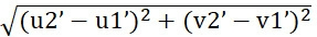
值得注意的是,若第一反射元件310以及第二反射元件320的
在一些實施例中,第一反射元件310的色度坐標(u1’,v1’)指的是測量第一反射元件310的色度坐標三次得到的平均值,並且第一反射元件310的三個色度坐標可以分別藉由測量第一反射元件310的不同位置得到。在一些實施例中,第二反射元件320的色度坐標(u2’,v2’)指的是測量光反射區域100R中的第二反射元件320的色度坐標三次得到的平均值,並且第二反射元件320的三個色度坐標可以分別藉由測量光反射區域100R中的第二反射元件320的不同位置得到。In some embodiments, the chromaticity coordinates (u1', v1') of the first
在一些實施例中,可以使用角度分析儀(例如,DMS系列角度分析儀,如DMS 803或DMS 903)或其他儀器測量第一反射元件310(及/或第二反射元件320)的反射率及/或色度。舉例而言,角度分析儀的光源可包含可見光(例如,波長的範圍介於380nm及780nm之間),但不限於此。在一些實施例中,光源可包含鹵素燈或其他合適的光源,且光源的光譜如第3圖所示,但不限於此。承前述,在一些實施例中,第一反射元件310的第一反射率R1是在去除第一黏著層(未繪示)之後進行測量,此同樣適用於色度的測量。在一些實施例中,可以使用其他合適的儀器測量第一反射元件310(及/或第二反射元件320)的反射率及/或色度。In some embodiments, an angle analyzer (for example, a DMS series angle analyzer, such as DMS 803 or DMS 903) or other instruments can be used to measure the reflectivity and / or chroma. For example, the light source of the angle analyzer may include visible light (eg, the wavelength range is between 380 nm and 780 nm), but is not limited thereto. In some embodiments, the light source may include a halogen lamp or other suitable light sources, and the spectrum of the light source is as shown in FIG. 3 , but is not limited thereto. Based on the foregoing, in some embodiments, the first reflectance R1 of the first
表1以及表2顯示第一反射元件310在去除第一黏著層之前與之後(有與沒有第一黏著層)的反射率以及色度的測量結果。Table 1 and Table 2 show the measurement results of reflectivity and chromaticity of the first
表1
表2

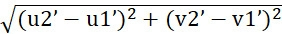
如表1以及表2所示,第一反射元件310在去除第一黏著層之前與之後(有與沒有第一黏著層)的反射率以及色度的測量結果相似。此外,去除第一黏著層之前與之後(有與沒有第一黏著層)的第一反射率R1以及第二反射率R2所得到的│(R1-R2)│/Max(R1,R2)的值滿足前述公式,即0 ≤ │(R1-R2)│/Max(R1, R2) < 20%。去除第一黏著層之前與之後(有與沒有第一黏著層)得到的色度坐標u1’、v1’、u2’、v2’滿足下列公式:0 ≤
請再次參照第1圖以及第2A圖,在一些實施例中,於上視圖中(與沿電路板100的法線方向Z相同),第二反射元件320的一部分可與第一反射元件310重疊。藉由此種配置,可以增加第一反射元件310以及第二反射元件320的錯位容許偏差。Please refer to FIG. 1 and FIG. 2A again, in some embodiments, in a top view (same as along the normal direction Z of the circuit board 100), a part of the second
在一些實施例中,第二反射元件320的形狀可為T形。在一些實施例中,第二反射元件320的一部分可以設置於光反射區域100R中,而在電路板100的法線方向Z上,第二反射元件320的另一部分可以與發光元件200重疊。In some embodiments, the second
在一些實施例中,電路板100可具有與導光板110相鄰且沿第一方向X延伸的側邊100S,在電路板100的法線方向Z上,電路板100的側邊100S可與導光板110重疊。在垂直於第一方向X的第二方向Y上,複數個發光元件200的其中一者與電路板100的側邊100S之間可具有第一距離L
LB,再者,第二反射元件320在第二方向Y上可具有寬度L
PI,且第一距離L
LB以及第二反射元件320的寬度L
PI滿足下列公式:0.5 ≤ L
PI/L
LB≤ 1,亦即,寬度L
PI與第一距離L
LB的比值可以大於或等於0.5且小於或等於1,例如,0.6、0.7、0.8或0.9,但不限於此。
In some embodiments, the
值得注意的是,若L
PI/L
LB的比值過小(例如,小於0.5),則電路板100的暴露面積可能會過大,因此可能會產生色偏(color-shifting)問題。
It should be noted that if the ratio of L PI /L LB is too small (for example, less than 0.5), the exposed area of the
在一些實施例中,第一距離L
LB指的是在第二方向Y上,複數個發光面200S的其中一者與電路板100的側邊100S之間的距離,此外,第一距離L
LB指的是在不同位置測量光反射區域100R中的發光面200S與側邊100S之間的距離三次所得到的平均值。在一些實施例中,寬度L
PI指的是測量第二反射元件320在第二方向Y上的寬度三次所得到的平均值,並且三個寬度L
PI可以分別在不同位置測量得到。再者,當第二反射元件320具有與發光元件200重疊的其他部分時,計算平均值時選擇的第二反射元件320的寬度應不包含沿電路板100的法線方向Z與發光元件200重疊的第二反射元件320的其他部分。
In some embodiments, the first distance L LB refers to the distance between one of the plurality of light emitting
在一些實施例中,第二反射元件320可具有第一側邊320S-1,第一側邊320S-1可鄰近發光元件200並沿第一方向X延伸。在一些實施例中,在垂直於第一方向X的第二方向Y上,第二反射元件320的第一側邊320S-1與複數個發光元件200的其中一者之間可具有距離d,且距離d滿足下列公式:0 ≤ d ≤ 0.5mm,亦即,第一側邊320S-1與發光元件200之間的距離d可以大於或等於0且小於或等於0.5mm,例如,0.1mm、0.2mm、0.3mm或0.4mm,但不限於此。值得注意的是,若第一側邊320S-1與發光元件200之間的距離d過大(例如,大於0.5mm),則電路板100暴露的面積可能會過大,因此在發光面200S附近可能會產生色帶(color band),或背光模組10可能會發光色偏問題。In some embodiments, the second
此外,距離d指的是測量光反射區域100R中的第一側邊320S-1與發光面200S之間的距離三次所得到的平均值,並且三個距離d可以分別在不同位置測量得到。再者,計算平均值時選擇的距離d應不包含沿電路板100的法線方向Z與發光元件200重疊的第二反射元件320的其他部分。In addition, the distance d refers to the average value obtained by measuring the distance between the
在一些實施例中,第二反射元件320可以具有第二側邊320S-2,第二側邊320S-2與第一側邊320S-1相對且沿第一方向X延伸。在一些實施例中,第二反射元件320的第二側邊320S-2可鄰近電路板100的側邊100S。在一些實施例中,在垂直於第一方向X的第二方向Y上,第二側邊320S-2與電路板100的側邊100S之間可具有距離d2。在一些實施例中,距離d2可以大於0,亦即,在電路板100的法線方向Z上,第二側邊320S-2可不與側邊100S重疊。舉例而言,在第二方向Y上,側邊100S可以突出於第二側邊320S-2。In some embodiments, the second
承前述,在一些實施例中,第二反射元件320可以不與光反射區域100R中的導光板110接觸(如第2B圖所示)。具體而言,在電路板100的法線方向Z上,第二反射元件320與導光板110之間可具有距離d1。在電路板100的法線方向Z上,距離d1實質上可與第一反射元件310的厚度相同(如第2A圖所示)。在一些實施例中,距離d1可滿足下列公式:0 < 距離d1 ≤ 200μm。在一些實施例中,距離d1可以大於或等於50μm且小於或等於100μm,例如60μm、70μm、80μm或90μm,但不限於此。Based on the foregoing, in some embodiments, the second
值得注意的是,若第二反射元件320與導光板110之間的距離dl過大(例如,大於200μm),則從發光元件200傳送至導光板110的光量可能會減少。It should be noted that if the distance d1 between the second
在一些實施例中,距離dl指的是在任一剖面中測量第二反射元件320與導光板110之間的距離三次得到的平均值,並且三個距離dl可以分別在不同位置測量得到。In some embodiments, the distance d1 refers to an average value obtained by measuring the distance between the second
請參照第2A圖以及第2B圖,在一些實施例中,第三反射元件120的材料可包含金屬、白色材料(例如,白色墨水、白色膠帶)、其他合適的反射材料或前述之組合,但不限於此。第三反射元件120可以具有第三反射率R3。在一些實施例中,第三反射元件120的第三反射率R3可以大於第二反射元件320的第二反射率R2。值得注意的是,若第三反射率R3小於第二反射率R2,則可能會形成亮帶(bright band),因此可能會影響背光模組10的光學品質。Please refer to FIG. 2A and FIG. 2B. In some embodiments, the material of the third
在一些實施例中,第二反射率R2以及第三反射率R3滿足下列公式:0 ≤ │(R2-R3)│/Max(R2,R3) < 50%,亦即,第二反射率R2與第三反射率R3的差值的絕對值與第二反射率R2或第三反射率R3的最大值(第二反射率R2以及第三反射率R3中較大者)之比值可以大於或等於0且小於50%。在一些實施例中,│(R2-R3)│/Max(R2,R3)的值可以大於或等於10%且小於或等於45%,例如,為15%、20%、25%、30%、35%或40%,但不限於此。In some embodiments, the second reflectivity R2 and the third reflectivity R3 satisfy the following formula: 0 ≤ │(R2-R3)│/Max(R2, R3) < 50%, that is, the second reflectivity R2 and The ratio of the absolute value of the difference of the third reflectivity R3 to the maximum value of the second reflectivity R2 or the third reflectivity R3 (the larger of the second reflectivity R2 and the third reflectivity R3) may be greater than or equal to 0 And less than 50%. In some embodiments, the value of │(R2-R3)│/Max(R2, R3) may be greater than or equal to 10% and less than or equal to 45%, for example, 15%, 20%, 25%, 30%, 35% or 40%, but not limited to.
更具體而言,在一實施例中,第二反射率R2可為52.10%,第三反射率R3可為99%,且│(R2-R3)│/Max(R2,R3)的值可為47.37%。在另一實施例中,第二反射率R2可為63.17%,第三反射率R3可為99%,且│(R2-R3)│/Max(R2,R3)的值可為36.19%。More specifically, in one embodiment, the second reflectivity R2 can be 52.10%, the third reflectivity R3 can be 99%, and the value of │(R2-R3)│/Max(R2, R3) can be 47.37%. In another embodiment, the second reflectivity R2 may be 63.17%, the third reflectivity R3 may be 99%, and the value of │(R2−R3)│/Max(R2, R3) may be 36.19%.
值得注意的是,若│(R2-R3)│/Max(R2,R3)的值過大(例如,大於50%),則背光模組10的光提取效率可能會降低,再者,可能會形成亮帶或暗帶(dark band),進而影響背光模組10的光學品質。It is worth noting that if the value of │(R2-R3)│/Max(R2, R3) is too large (for example, greater than 50%), the light extraction efficiency of the
此外,在一些實施例中,第三反射率R3指的是測量第三反射元件120的反射率三次得到的平均值,並且第三反射元件120的三個反射率可以分別藉由測量第三反射元件120的不同位置得到。In addition, in some embodiments, the third reflectivity R3 refers to the average value obtained by measuring the reflectivity of the third
接著,請參照第4圖,第4圖顯示根據本揭露一些實施例中,背光模組10的發光元件200的剖面結構示意圖。第4圖繪示發光元件200的示例性結構,但本揭露不以此為限。Next, please refer to FIG. 4 , which shows a schematic cross-sectional structure diagram of the
承前述,在一些實施例中,發光元件200可為無機發光二極體。發光元件200可包含基板202、第一半導體層206、量子井(quantum well)層208、第二半導體層210、導電層212、第一電極214a以及第二電極214b,但不以此為限。Based on the foregoing, in some embodiments, the
此外,發光元件200的第一電極214a以及第二電極214b可以藉由電路板100的導電墊216(如第1圖以及第2B圖所示)與電路板100電性連接。In addition, the
在一些實施例中,第一半導體層206可為n型半導體或p型半導體的其中一種,而第二半導體層210可為n型半導體或p型半導體的另一種。n型半導體可包含摻雜有四價原子的氮化鎵(n-GaN)或磷化鋁銦(n-AlInP),但不限於此。p型半導體可包含摻雜有二價原子的氮化鎵(p-GaN)或磷化鋁銦(p-AlInP),但不限於此。在一些實施例中,量子井層208可包含單量子井(single quantum well,SQW)或多量子井(multiple quantum well,MQW)。量子井層208的材料可包含氮化鎵、磷化鋁銦(AlInP)、氮化銦鎵(InGaN)或前述之組合,但不限於此。In some embodiments, the
在一些實施例中,導電層212的材料可包含透明導電材料,例如,氧化銦錫(indium tin oxide,ITO)、氧化錫(tin oxide,SnO)、氧化鋅(zinc oxide,ZnO)、氧化銦鋅(indium zinc oxide,IZO)、氧化銦鎵鋅(indium gallium zinc oxide,IGZO)、氧化銦錫鋅(indium tin zinc oxide,ITZO)、氧化銻錫(antimony tin oxide,ATO)、氧化銻鋅(antimony zinc oxide,AZO)、其他合適的透明導電材料或前述之組合,但不限於此。在一些實施例中,第一電極214a以及第二電極214b的材料可包含金屬導電材料。In some embodiments, the material of the
應理解的是,第4圖中的發光元件200可進一步包含封裝組件(未繪示),第4圖繪示發光元件200的裸晶。此外,雖然第4圖所繪示的發光元件200具有垂直型(vertical type)結構,但在另一些實施例中,發光元件200也可以具有覆晶型(flip-chip type)結構。It should be understood that the
於下文中與前文相同或相似的組件或元件將以相同或相似之標號表示,其材料、製造方法與功能與前文所述相同或相似,故此部分於下文中將不再贅述。Components or elements that are the same or similar to those described above will be denoted by the same or similar symbols, and their materials, manufacturing methods, and functions are the same or similar to those described above, so this part will not be described in detail below.
請參照第5圖,第5圖顯示根據本揭露另一些實施例中,背光模組20的局部上視結構示意圖。如第5圖所示,在一些實施例中,於至少一個光反射區域100R中,第二反射元件320的第一側邊320S-1與發光面200S之間在第二方向Y上可以沒有距離。換言之,在電路板100的法線方向Z上,第二反射元件320的一部分(例如,第二側邊320S-2)實質上可與複數個發光元件200的其中一者重疊。因此,在第二方向Y上,第二側邊320S-2與電路板100的側邊100S之間的距離d2可以為零。此外,其中一個發光元件200與側邊100S之間的第一距離L
LB實質上可與第二反射元件320在第二方向Y上的寬度L
PI相同。
Please refer to FIG. 5 . FIG. 5 shows a partial top-view structure diagram of the
請參照第6圖,第6圖顯示根據本揭露另一些實施例中,背光模組30的局部上視結構示意圖。如第6圖所示,在一些實施例中,第二反射元件320的形狀實質上可為長條形(strip shape),在第二方向Y上,第二反射元件320的第一側邊320S-1與發光面200S之間可以具有距離d。第一距離L
LB可以大於寬度L
PI,亦即,在第二方向Y上,第二側邊320S-2與側邊100S之間可具有距離d2。在一些實施例中,在電路板100的法線方向Z上,第一反射元件310可不與光反射區域100R重疊。
Please refer to FIG. 6 . FIG. 6 shows a partial top structural schematic view of the
請參照第7圖,第7圖顯示根據本揭露另一些實施例中,背光模組40的局部上視結構示意圖。如第7圖所示,在一些實施例中,於第二方向Y上,光反射區域100R中的第二反射元件320的第一側邊320S-1與發光元件200的發光面200S之間可以不具有距離。在一些實施例中,在電路板100的法線方向Z上,第二反射元件320可與發光元件200部分地重疊。此外,在第二方向Y上,第一反射元件310可稍微向外突出於電路板的側邊100S(或第二反射元件320的第二側邊320S-2)。換言之,在電路板100的法線方向Z上,第一反射元件310的一部分可不與電路板100重疊。在一些實施例中,發光元件200與側邊100S之間的第一距離L
LB實質上可與第二反射元件320在第二方向Y上的寬度L
PI相同。在一些實施例中,在電路板100的法線方向Z上,第一反射元件310可不與光反射區域100R重疊。
Please refer to FIG. 7 . FIG. 7 shows a partial top-view structure diagram of the
請參照第8圖,第8圖顯示根據本揭露另一些實施例中,背光模組50的局部上視結構示意圖。如第8圖所示,在一些實施例中,第一反射元件310可圍繞一或複數個發光元件200,且在電路板100的法線方向Z上與一或複數個光反射區域100R的至少一部分重疊。在電路板100的法線方向Z上,第一反射元件310可以與電路板100的側邊100S重疊。在一些實施例中,第一反射元件310的形狀可為網格形(grid),第一反射元件310可具有開口AP,且在電路板100的法線方向Z上,第二反射元件320可與第一反射元件310的開口AP重疊。Please refer to FIG. 8 . FIG. 8 shows a partial top-view structure diagram of a
請參照第9圖,第9圖顯示根據本揭露另一些實施例中,背光模組60的局部上視結構示意圖。如第9圖所示,在一些實施例中,第一反射元件310可具有彼此分離的複數個子部分(sub-part)310S,複數個子部分310S的至少一者的形狀可為錐形(tapered shape)或子彈形(bullet shape)。子部分310S可分別設置於發光元件200之間,且在電路板100的法線方向Z上不與光反射區域100R重疊。在一些實施例中,第一反射元件310的子部分310S與發光元件200可以沿第一方向X交替排列。再者,電路板100可以具有第一部分P1以及與第一部分P1連接的第二部分P2,第一部分P1可以沿第一方向X延伸,且第二部分P2可以沿第二方向Y延伸。發光元件200可設置於第一部分P1上,而第二部分P2可遠離電路板100的側邊100S。在一些實施例中,第二反射元件320的一部分在電路板100的法線方向Z上可以與第一部分P1重疊,但第二反射元件320的所述部分在電路板100的法線方向Z上可以不與電路板100的導電墊216(如第1圖所示)重疊。在一些實施例中,在電路板100的法線方向Z上,第二反射元件320可以與第二部分P2的一部分重疊,並且不與第二反射元件320重疊的第二部分P2的另一部分可以作為連接件400。在一些實施例中,外部信號可以藉由連接件400傳輸到發光元件200。Please refer to FIG. 9 . FIG. 9 shows a partial top structural schematic view of the
請參照第10圖,第10圖顯示根據本揭露另一些實施例中,背光模組70的局部上視結構示意圖。如第10圖所示,在一些實施例中,第二反射元件320的形狀可為長條形,光反射區域100R中的第二反射元件320的第一側邊320S-1與發光元件200的發光面200S之間可以不具有距離。在一些實施例中,在第二方向Y上,第一反射元件310的一部分可以突出於第二反射元件320的第二側320S-2。換言之,第一反射元件310與側邊100S之間在第二方向Y上的最小距離d3可小於第二側邊320S-2與電路板100的側邊100S之間在第二方向Y上的距離d2。此外,發光元件200與側邊100S之間的第一距離L
LB可大於第二反射元件320的寬度L
PI。在一些實施例中,第一反射元件310在電路板100的法線方向Z上可以不與電路板100的側邊100S重疊,第一反射元件310在Y方向上可突出於電路板100的側邊100S。換言之,第一反射元件310與側邊100S之間具有最小距離d3。
Please refer to FIG. 10 . FIG. 10 shows a partial top view structural diagram of the
綜上所述,根據本揭露的一些實施例,背光模組包含以特定配置排列的的第一反射元件以及第二反射元件。此外,第一反射元件以及第二反射元件的反射率經設計以符合特定的公式。藉由此種特定的配置,可以改善背光模組的光提取效率,因此,可以增強電子裝置的效能或可靠性。To sum up, according to some embodiments of the present disclosure, the backlight module includes first reflective elements and second reflective elements arranged in a specific configuration. In addition, the reflectivity of the first reflective element and the second reflective element is designed to meet a specific formula. With this specific configuration, the light extraction efficiency of the backlight module can be improved, and therefore, the performance or reliability of the electronic device can be enhanced.
雖然本揭露的實施例及其優點已揭露如上,但應該瞭解的是,任何所屬技術領域中具有通常知識者,在不脫離本揭露之精神和範圍內,當可作更動、替代與潤飾。本揭露實施例之間的特徵只要不違背發明精神或相衝突,均可任意混合搭配使用。此外,本揭露之保護範圍並未侷限於說明書內所述特定實施例中的製程、機器、製造、物質組成、裝置、方法及步驟,任何所屬技術領域中具有通常知識者可從本揭露揭示內容中理解現行或未來所發展出的製程、機器、製造、物質組成、裝置、方法及步驟,只要可以在此處所述實施例中實施大抵相同功能或獲得大抵相同結果皆可根據本揭露使用。因此,本揭露之保護範圍包含上述製程、機器、製造、物質組成、裝置、方法及步驟。本揭露之保護範圍當視後附之發明申請專利範圍所界定者為準。本揭露的任一實施例或請求項不須達成本揭露所公開的全部目的、優點、特點。Although the embodiments of the present disclosure and their advantages have been disclosed above, it should be understood that those skilled in the art can make changes, substitutions and modifications without departing from the spirit and scope of the present disclosure. The features of the disclosed embodiments can be mixed and matched arbitrarily as long as they do not violate the spirit of the invention or conflict with each other. In addition, the protection scope of the present disclosure is not limited to the process, machine, manufacture, material composition, device, method and steps in the specific embodiments described in the specification, and anyone with ordinary knowledge in the technical field can learn from the content of the present disclosure It is understood that the current or future developed process, machine, manufacture, material composition, device, method and step can be used according to the present disclosure as long as it can perform substantially the same function or obtain substantially the same result in the embodiments described herein. Therefore, the protection scope of the present disclosure includes the above-mentioned process, machine, manufacture, composition of matter, device, method and steps. The scope of protection of this disclosure shall be subject to the scope defined in the appended patent application for invention. Any embodiment or claim item of the present disclosure does not need to achieve all the objectives, advantages and features disclosed in the present disclosure.
10、20、30、40、50、60、70:背光模組
100:電路板
100S:側邊
100R:光反射區域
110:導光板
120:第三反射元件
200:發光元件
200S:發光面
202:基板
206:第一半導體層
208:量子井層
210:第二半導體層
212:導電層
214a:第一電極
214b:第二電極
216:導電墊
310:第一反射元件
310S:子部分
320:第二反射元件
320S-1:第一側邊
320S-2:第二側邊
400:連接件
A-A’:截線
AP:開口
B-B’:截線
d:距離
d1:距離
d2:距離
d3:最小距離
DP:顯示面板
EX1:虛擬線
EX2:虛擬線
L
LB:第一距離
L
PI:寬度
P1:第一部分
P2:第二部分
W
200:最大寬度
VL1:虛擬線
10, 20, 30, 40, 50, 60, 70: backlight module 100:
第1圖顯示根據本揭露一些實施例中,背光模組的局部上視結構示意圖; 第2A圖顯示根據本揭露一些實施例中,對應於第1圖中的截線A-A’的背光模組的剖面結構示意圖; 第2B圖顯示根據本揭露一些實施例中,對應於第1圖中的截線B-B’的背光模組的剖面結構示意圖; 第3圖顯示根據本揭露一些實施例中,用於測量反射率以及色度(chromaticity)的光源的光譜; 第4圖顯示根據本揭露一些實施例中,背光模組的發光元件的剖面結構示意圖; 第5圖顯示根據本揭露一些實施例中,背光模組的局部上視結構示意圖; 第6圖顯示根據本揭露一些實施例中,背光模組的局部上視結構示意圖; 第7圖顯示根據本揭露一些實施例中,背光模組的局部上視結構示意圖; 第8圖顯示根據本揭露一些實施例中,背光模組的局部上視結構示意圖; 第9圖顯示根據本揭露一些實施例中,背光模組的局部上視結構示意圖; 第10圖顯示根據本揭露一些實施例中,背光模組的局部上視結構示意圖。 FIG. 1 shows a partial top-view structure diagram of a backlight module according to some embodiments of the present disclosure; FIG. 2A shows a schematic cross-sectional structure diagram of a backlight module corresponding to section line A-A' in FIG. 1 according to some embodiments of the present disclosure; Figure 2B shows a schematic cross-sectional structure diagram of a backlight module corresponding to the section line B-B' in Figure 1 according to some embodiments of the present disclosure; Figure 3 shows the spectrum of a light source used to measure reflectance and chromaticity according to some embodiments of the present disclosure; FIG. 4 shows a schematic cross-sectional structure diagram of a light emitting element of a backlight module according to some embodiments of the present disclosure; FIG. 5 shows a partial top-view structure diagram of a backlight module according to some embodiments of the present disclosure; FIG. 6 shows a partial top-view structure diagram of a backlight module according to some embodiments of the present disclosure; FIG. 7 shows a partial top-view structure diagram of a backlight module according to some embodiments of the present disclosure; FIG. 8 shows a partial top-view structure diagram of a backlight module according to some embodiments of the present disclosure; FIG. 9 shows a partial top-view structure diagram of a backlight module according to some embodiments of the present disclosure; FIG. 10 shows a partial top-view structure diagram of a backlight module according to some embodiments of the present disclosure.
10:背光模組 10: Backlight module
100:電路板 100: circuit board
100S:側邊 100S: side
100R:光反射區域 100R: light reflection area
110:導光板 110: light guide plate
200:發光元件 200: light emitting element
200S:發光面 200S: Luminous surface
216:導電墊 216: Conductive pad
310:第一反射元件 310: first reflective element
320:第二反射元件 320: second reflective element
320S-1:第一側邊 320S-1: First side
320S-2:第二側邊 320S-2: Second side
A-A’:截線 A-A': truncated line
B-B’:截線 B-B': truncated line
d:距離 d: distance
d2:距離 d2: distance
EX1:虛擬線 EX1: virtual line
EX2:虛擬線 EX2: virtual line
LLB:第一距離 L LB : first distance
LPI:寬度 L PI : Width
W200:最大寬度 W 200 : Maximum width
VL1:虛擬線 VL1: virtual line
Claims (20)

Applications Claiming Priority (2)
| Application Number | Priority Date | Filing Date | Title |
|---|---|---|---|
| US17/344,580 US11397350B1 (en) | 2021-06-10 | 2021-06-10 | Backlight module and electronic device including the same |
| US17/344,580 | 2021-06-10 |
Publications (2)
| Publication Number | Publication Date |
|---|---|
| TW202248564A true TW202248564A (en) | 2022-12-16 |
| TWI806654B TWI806654B (en) | 2023-06-21 |
Family
ID=82484060
Family Applications (1)
| Application Number | Title | Priority Date | Filing Date |
|---|---|---|---|
| TW111121629A TWI806654B (en) | 2021-06-10 | 2022-06-10 | Backlight module and electronic device including the same |
Country Status (2)
| Country | Link |
|---|---|
| US (4) | US11397350B1 (en) |
| TW (1) | TWI806654B (en) |
Families Citing this family (1)
| Publication number | Priority date | Publication date | Assignee | Title |
|---|---|---|---|---|
| CN118959936B (en) * | 2024-08-30 | 2025-05-06 | 绵阳惠科光电科技有限公司 | Bracket, backlight module and display device |
Family Cites Families (14)
| Publication number | Priority date | Publication date | Assignee | Title |
|---|---|---|---|---|
| DE10245933B4 (en) * | 2002-09-30 | 2013-10-10 | Osram Opto Semiconductors Gmbh | Device for generating a bundled luminous flux |
| TWI364557B (en) * | 2008-05-02 | 2012-05-21 | Chimei Innolux Corp | Light source and backlight module and liquid crystal display device using same |
| TWI418899B (en) * | 2010-10-12 | 2013-12-11 | Au Optronics Corp | Liquid crystal display and back-light module thereof |
| TWI465808B (en) * | 2010-11-25 | 2014-12-21 | Lg伊諾特股份有限公司 | Backlight unit and display apparatus using the same |
| TWI435145B (en) * | 2010-12-15 | 2014-04-21 | Au Optronics Corp | Light source circuit module, backlight module, and display apparatus with reflective structure of light |
| US9752753B2 (en) * | 2012-03-14 | 2017-09-05 | Samsung Display Co., Ltd. | Display device comprising the same |
| TWI472850B (en) | 2012-05-08 | 2015-02-11 | Au Optronics Corp | Backlight module |
| WO2014188748A1 (en) * | 2013-05-24 | 2014-11-27 | シャープ株式会社 | Lighting device and display device |
| CN104061492A (en) * | 2014-05-23 | 2014-09-24 | 京东方科技集团股份有限公司 | Light bar, backlight and display device |
| KR20160070903A (en) * | 2014-12-10 | 2016-06-21 | 삼성디스플레이 주식회사 | Display apparatus |
| CN109312906A (en) * | 2016-05-04 | 2019-02-05 | 亮锐控股有限公司 | Molded light guides for optical coupling of light from LEDs |
| CN207976672U (en) | 2018-02-11 | 2018-10-16 | 扬昕科技(苏州)有限公司 | light source module and display |
| TW202036060A (en) * | 2018-11-12 | 2020-10-01 | 美商康寧公司 | Backlight including patterned reflectors, diffuser plate, and method for fabricating the backlight |
| TWI686633B (en) * | 2019-04-09 | 2020-03-01 | 佳世達科技股份有限公司 | Backlight module |
-
2021
- 2021-06-10 US US17/344,580 patent/US11397350B1/en active Active
-
2022
- 2022-06-10 TW TW111121629A patent/TWI806654B/en active
- 2022-06-22 US US17/846,822 patent/US11703713B2/en active Active
-
2023
- 2023-05-31 US US18/326,466 patent/US20230305331A1/en not_active Abandoned
-
2025
- 2025-04-17 US US19/182,493 patent/US20250244623A1/en active Pending
Also Published As
| Publication number | Publication date |
|---|---|
| US20230305331A1 (en) | 2023-09-28 |
| US20220404669A1 (en) | 2022-12-22 |
| US11703713B2 (en) | 2023-07-18 |
| US20250244623A1 (en) | 2025-07-31 |
| US11397350B1 (en) | 2022-07-26 |
| TWI806654B (en) | 2023-06-21 |
Similar Documents
| Publication | Publication Date | Title |
|---|---|---|
| JP4757477B2 (en) | Light source unit, illumination device using the same, and display device using the same | |
| US11092849B2 (en) | LED backlight device and display device | |
| CN111199685B (en) | Splicing devices and electronics | |
| CN111863874A (en) | display device | |
| KR102747582B1 (en) | Light source member, display device including the same, and manufacturing method for the same | |
| US10551668B2 (en) | Liquid crystal display panel with border areas of miniscule dimensions | |
| US11387387B2 (en) | Micro light emitting device display apparatus | |
| US20210183833A1 (en) | Electronic device | |
| US11742335B2 (en) | Electronic device | |
| US11703918B2 (en) | Electronic device | |
| CN108664165A (en) | The electronic device of display panel and the application display panel | |
| US20250244623A1 (en) | Light-emitting device | |
| TWI803252B (en) | Backlight module and electronic device | |
| TWI749851B (en) | Display device | |
| PH12019000058A1 (en) | Display device | |
| CN109962080A (en) | display device | |
| CN110838500B (en) | Micro light-emitting diode display device | |
| TW202238239A (en) | Backlight module and display device | |
| US11003025B2 (en) | Backlight unit and display device including the same | |
| US11714314B2 (en) | Illumination device and display device | |
| CN110164854A (en) | Lighting device | |
| JP4781246B2 (en) | Light emitting device package, surface light emitting device and display device | |
| TW202042202A (en) | Display device | |
| KR102917219B1 (en) | Light emitting device package and display device using same | |
| CN106195759A (en) | Light emitting module and display device |